EP2888629B1 - Method for microcontact printing - Google Patents
Method for microcontact printing Download PDFInfo
- Publication number
- EP2888629B1 EP2888629B1 EP13799316.8A EP13799316A EP2888629B1 EP 2888629 B1 EP2888629 B1 EP 2888629B1 EP 13799316 A EP13799316 A EP 13799316A EP 2888629 B1 EP2888629 B1 EP 2888629B1
- Authority
- EP
- European Patent Office
- Prior art keywords
- stamp
- embossing
- mpa
- molecular component
- die
- Prior art date
- Legal status (The legal status is an assumption and is not a legal conclusion. Google has not performed a legal analysis and makes no representation as to the accuracy of the status listed.)
- Active
Links
- 238000000034 method Methods 0.000 title claims description 34
- 238000000813 microcontact printing Methods 0.000 title description 2
- 238000004049 embossing Methods 0.000 claims description 57
- 239000000463 material Substances 0.000 claims description 48
- 239000000758 substrate Substances 0.000 claims description 12
- 239000011148 porous material Substances 0.000 claims description 8
- 108090000765 processed proteins & peptides Proteins 0.000 claims description 6
- 239000004205 dimethyl polysiloxane Substances 0.000 claims description 4
- 229920000435 poly(dimethylsiloxane) Polymers 0.000 claims description 4
- 229920000642 polymer Polymers 0.000 claims description 4
- 102000004196 processed proteins & peptides Human genes 0.000 claims description 4
- 102000004190 Enzymes Human genes 0.000 claims description 3
- 108090000790 Enzymes Proteins 0.000 claims description 3
- BLRPTPMANUNPDV-UHFFFAOYSA-N Silane Chemical compound [SiH4] BLRPTPMANUNPDV-UHFFFAOYSA-N 0.000 claims description 3
- 150000001336 alkenes Chemical class 0.000 claims description 3
- 239000005556 hormone Substances 0.000 claims description 3
- 229940088597 hormone Drugs 0.000 claims description 3
- 239000003016 pheromone Substances 0.000 claims description 3
- 229910000077 silane Inorganic materials 0.000 claims description 3
- 150000004756 silanes Chemical class 0.000 claims description 3
- 239000011782 vitamin Substances 0.000 claims description 3
- 239000002253 acid Substances 0.000 claims description 2
- 150000001337 aliphatic alkines Chemical class 0.000 claims description 2
- 229930013930 alkaloid Natural products 0.000 claims description 2
- 235000014633 carbohydrates Nutrition 0.000 claims description 2
- 102000039446 nucleic acids Human genes 0.000 claims description 2
- 108020004707 nucleic acids Proteins 0.000 claims description 2
- 102000004169 proteins and genes Human genes 0.000 claims description 2
- 108090000623 proteins and genes Proteins 0.000 claims description 2
- 229940088594 vitamin Drugs 0.000 claims description 2
- 229930003231 vitamin Natural products 0.000 claims description 2
- 235000013343 vitamin Nutrition 0.000 claims description 2
- 150000001491 aromatic compounds Chemical class 0.000 claims 1
- 235000013870 dimethyl polysiloxane Nutrition 0.000 claims 1
- 229910021389 graphene Inorganic materials 0.000 claims 1
- CXQXSVUQTKDNFP-UHFFFAOYSA-N octamethyltrisiloxane Chemical compound C[Si](C)(C)O[Si](C)(C)O[Si](C)(C)C CXQXSVUQTKDNFP-UHFFFAOYSA-N 0.000 claims 1
- 238000004987 plasma desorption mass spectroscopy Methods 0.000 claims 1
- 230000008569 process Effects 0.000 description 11
- 239000010702 perfluoropolyether Substances 0.000 description 8
- 238000004519 manufacturing process Methods 0.000 description 7
- 238000009792 diffusion process Methods 0.000 description 5
- 230000008901 benefit Effects 0.000 description 4
- 239000012530 fluid Substances 0.000 description 4
- 239000000919 ceramic Substances 0.000 description 3
- 239000007788 liquid Substances 0.000 description 3
- 239000002184 metal Substances 0.000 description 3
- 238000001127 nanoimprint lithography Methods 0.000 description 3
- 239000002086 nanomaterial Substances 0.000 description 3
- 239000000047 product Substances 0.000 description 3
- 239000000126 substance Substances 0.000 description 3
- 150000001335 aliphatic alkanes Chemical class 0.000 description 2
- 230000005540 biological transmission Effects 0.000 description 2
- 238000001311 chemical methods and process Methods 0.000 description 2
- 238000002508 contact lithography Methods 0.000 description 2
- 230000008602 contraction Effects 0.000 description 2
- 238000011161 development Methods 0.000 description 2
- 230000018109 developmental process Effects 0.000 description 2
- 238000001459 lithography Methods 0.000 description 2
- 238000001682 microtransfer moulding Methods 0.000 description 2
- 230000010363 phase shift Effects 0.000 description 2
- 238000000206 photolithography Methods 0.000 description 2
- WIGIZIANZCJQQY-UHFFFAOYSA-N 4-ethyl-3-methyl-N-[2-[4-[[[(4-methylcyclohexyl)amino]-oxomethyl]sulfamoyl]phenyl]ethyl]-5-oxo-2H-pyrrole-1-carboxamide Chemical compound O=C1C(CC)=C(C)CN1C(=O)NCCC1=CC=C(S(=O)(=O)NC(=O)NC2CCC(C)CC2)C=C1 WIGIZIANZCJQQY-UHFFFAOYSA-N 0.000 description 1
- OKTJSMMVPCPJKN-UHFFFAOYSA-N Carbon Chemical compound [C] OKTJSMMVPCPJKN-UHFFFAOYSA-N 0.000 description 1
- 230000009471 action Effects 0.000 description 1
- 150000001345 alkine derivatives Chemical class 0.000 description 1
- 150000001720 carbohydrates Chemical class 0.000 description 1
- 238000005266 casting Methods 0.000 description 1
- 239000007795 chemical reaction product Substances 0.000 description 1
- 239000011248 coating agent Substances 0.000 description 1
- 238000000576 coating method Methods 0.000 description 1
- 238000001816 cooling Methods 0.000 description 1
- 238000005137 deposition process Methods 0.000 description 1
- 230000005489 elastic deformation Effects 0.000 description 1
- 229920001971 elastomer Polymers 0.000 description 1
- 239000000806 elastomer Substances 0.000 description 1
- 230000005684 electric field Effects 0.000 description 1
- 230000005670 electromagnetic radiation Effects 0.000 description 1
- 239000011888 foil Substances 0.000 description 1
- 239000007789 gas Substances 0.000 description 1
- 238000010438 heat treatment Methods 0.000 description 1
- 230000002045 lasting effect Effects 0.000 description 1
- 150000002632 lipids Chemical class 0.000 description 1
- 230000007246 mechanism Effects 0.000 description 1
- 238000005459 micromachining Methods 0.000 description 1
- 150000007523 nucleic acids Chemical class 0.000 description 1
- 230000035699 permeability Effects 0.000 description 1
- -1 polydimethylsiloxane Polymers 0.000 description 1
- 238000007639 printing Methods 0.000 description 1
- 230000009257 reactivity Effects 0.000 description 1
- 238000005096 rolling process Methods 0.000 description 1
- 238000000926 separation method Methods 0.000 description 1
- 238000002174 soft lithography Methods 0.000 description 1
- 239000007779 soft material Substances 0.000 description 1
- 239000002904 solvent Substances 0.000 description 1
- 230000008961 swelling Effects 0.000 description 1
- 238000003466 welding Methods 0.000 description 1
- 238000009736 wetting Methods 0.000 description 1
Images

Classifications
-
- G—PHYSICS
- G03—PHOTOGRAPHY; CINEMATOGRAPHY; ANALOGOUS TECHNIQUES USING WAVES OTHER THAN OPTICAL WAVES; ELECTROGRAPHY; HOLOGRAPHY
- G03F—PHOTOMECHANICAL PRODUCTION OF TEXTURED OR PATTERNED SURFACES, e.g. FOR PRINTING, FOR PROCESSING OF SEMICONDUCTOR DEVICES; MATERIALS THEREFOR; ORIGINALS THEREFOR; APPARATUS SPECIALLY ADAPTED THEREFOR
- G03F7/00—Photomechanical, e.g. photolithographic, production of textured or patterned surfaces, e.g. printing surfaces; Materials therefor, e.g. comprising photoresists; Apparatus specially adapted therefor
- G03F7/0002—Lithographic processes using patterning methods other than those involving the exposure to radiation, e.g. by stamping
-
- B—PERFORMING OPERATIONS; TRANSPORTING
- B82—NANOTECHNOLOGY
- B82Y—SPECIFIC USES OR APPLICATIONS OF NANOSTRUCTURES; MEASUREMENT OR ANALYSIS OF NANOSTRUCTURES; MANUFACTURE OR TREATMENT OF NANOSTRUCTURES
- B82Y10/00—Nanotechnology for information processing, storage or transmission, e.g. quantum computing or single electron logic
-
- B—PERFORMING OPERATIONS; TRANSPORTING
- B82—NANOTECHNOLOGY
- B82Y—SPECIFIC USES OR APPLICATIONS OF NANOSTRUCTURES; MEASUREMENT OR ANALYSIS OF NANOSTRUCTURES; MANUFACTURE OR TREATMENT OF NANOSTRUCTURES
- B82Y40/00—Manufacture or treatment of nanostructures
-
- G—PHYSICS
- G03—PHOTOGRAPHY; CINEMATOGRAPHY; ANALOGOUS TECHNIQUES USING WAVES OTHER THAN OPTICAL WAVES; ELECTROGRAPHY; HOLOGRAPHY
- G03F—PHOTOMECHANICAL PRODUCTION OF TEXTURED OR PATTERNED SURFACES, e.g. FOR PRINTING, FOR PROCESSING OF SEMICONDUCTOR DEVICES; MATERIALS THEREFOR; ORIGINALS THEREFOR; APPARATUS SPECIALLY ADAPTED THEREFOR
- G03F7/00—Photomechanical, e.g. photolithographic, production of textured or patterned surfaces, e.g. printing surfaces; Materials therefor, e.g. comprising photoresists; Apparatus specially adapted therefor
- G03F7/0015—Production of aperture devices, microporous systems or stamps
Description
Die vorliegende Erfindung betrifft ein Verfahren zum Mikrokontaktprägen gemäß Patentanspruch 1 oder 2.The present invention relates to a method for Mikrokontaktprägen according to
Der heutige Stand der Technik für die Mirko- und/oder Nanostrukturierung von Oberflächen umfasst vor allem die Photolithographie und die unterschiedlichen Prägetechniken. Die Prägetechniken arbeiten entweder mit harten oder weichen Stempeln. In letzter Zeit setzen sich vor allem die Prägelithographietechniken durch und verdrängen die klassischen Photolithographietechniken. Unter den Prägelithographietechniken wird vor allem die Verwendung von sogenannten weichen Stempeln immer beliebter. Der Grund liegt in der leichten Herstellung der Stempel, effizienten Prägevorgängen, sehr guten Oberflächeneigenschaften der jeweiligen Stempelmaterialien, den geringen Kosten, der Reproduzierbarkeit des Prägeproduktes und vor allem in der Möglichkeit der elastischen verformung des Stempels während der Entformung. In der Softlithographie wird ein Stempel aus einem Elastomer mit einer mikro- bzw. nanotrukturierten Oberfläche verwendet, um Strukturen im Bereich von 20 nm bis >1000 µm herzustellen. Die Prägelithographietechniken können grob in das Hot-Embossing, die Nanoimprintlithographie und das Nano- bzw. Mikrokontaktprägen eingeteilt werden. Beim Hot-Embossing wird der Stempel hauptsächlich unter Anwendung einer Kraft in eine (erwärmte) Prägemasse gedrückt. Bei der Nanoimprintlithographie wird ein sehr fein strukturierter Stempel mit der Prägemasse in Kontakt gebracht. Obwohl auch in diesem Verfahren Kräfte verwendet werden, ist die Aufnahme der Prägemasse in die nano- bzw. mikrometergroßen Strukturen durch kapillarwirkung eine treibende Kraft des Prägeprozesses. Beim Mikrokontaktprägen wird der strukturierte Stempel nicht durch Kraft in eine Prägemasse gedrückt, sondern überträgt eine an der Oberfläche seiner Strukturen befindliche Substanz auf eine andere Oberfläche.The current state of the art for the micro- and / or nanostructuring of surfaces mainly includes photolithography and the different embossing techniques. The stamping techniques work with either hard or soft stamps. Recently, especially the Prägelithographietechniken prevail and replace the classical photolithography techniques. Among the embossing lithography techniques, especially the use of so-called soft stamps is becoming increasingly popular. The reason lies in the easy production of the stamp, efficient embossing processes, very good surface properties of the respective stamp materials, the low cost, the reproducibility of the stamping product and, above all, the possibility of elastic deformation of the stamp during demoulding. In soft lithography, a stamp made of an elastomer having a micro- or nanostructured surface is used to produce structures in the range from 20 nm to> 1000 μm. The embossing lithography techniques can be broadly classified into hot embossing, nanoimprint lithography, and nano or microcontact embossing. When hot embossing is the Stamp pressed mainly by applying a force in a (heated) Prägemasse. In nanoimprint lithography, a very finely structured stamp is brought into contact with the embossing mass. Although forces are also used in this process, the inclusion of the embossing mass in the nano- or micrometer-sized structures by capillary action is a driving force of the embossing process. In microcontact embossing, the structured stamp is not forced by force into an embossing mass, but transfers a substance located on the surface of its structures to another surface.
Es gibt sechs bekannte Mikrokontaktprägeverfahren:
- Mikro- und/oder Nanokontaktdrucken (µ/nCP)
- Replikagießen (REM)
- Microtransfer moulding (µTM) oder nanoimprint lithographie (NIL),
- Mikroformung in Kapillaren (MIMIC)
- lösungsmittelunterstützten Mikroformen(SAMIM) und
- Phaseshift Lithographie.
- Micro and / or nanocontact printing (μ / nCP)
- Replica casting (REM)
- Microtransfer molding (μTM) or nanoimprint lithography (NIL),
- Micromachining in capillaries (MIMIC)
- Solvent - assisted microforms (SAMIM) and
- Phaseshift lithograph.
Elastomere Strukturstempel werden als Negativ eines Masters hergestellt. Beim Masterstempel handelt es sich um einen Hartstempel aus Metall oder Keramik, der durch entsprechend aufwendige Prozesse einmal hergestellt wird. Aus dem Master können dann beliebig viele Elastomere Stempel hergestellt werden. Die elastomeren Stempel ermöglichen einen konformen, gleichmäßigen Kontakt über große Oberflächen. Sie sind leicht von ihrem starren Masterstempel, sowie von den Prägeprodukten zu trennen. Weiterhin haben elastomere Stempel eine geringe Oberflächenspannung für eine leichte und einfache Trennung von Stempel und Substrat. Technische Probleme bereiten die Materialkombinationen des Strukturstempels und des Prägematerials, wobei es unter anderem auf eine Langlebigkeit beziehungsweise lange Verwendbarkeit des Strukturstempels und eine exakte Übertragung der Mikro- und/oder Nanostrukturen ankommt.Elastomeric structure stamps are produced as negative of a master. The master stamp is a hard stamp made of metal or ceramic, which is produced by correspondingly complex processes once. From the master then any number of elastomeric stamp can be produced. The elastomeric punches allow conformal, uniform contact over large surfaces. They are easily separated from their rigid master stamp, as well as the stamping products. Furthermore, elastomeric punches have a low surface tension for easy and easy separation of punch and substrate. Technical problems cause the material combinations of the structure stamp and the embossing material, whereby, among other things, on a longevity or long usability of the structure stamp and an exact transfer of the micro and / or nanostructures arrives.
Aufgabe der vorliegenden Erfindung ist es daher, ein Mikrokontaktdruckverfahren anzugeben, mit welchem ein langlebiger Strukturstempel angegeben wird, der für eine exakte Übertragung der Mikro- und/oder Nanostrukturen auf großen Flächen geeignet ist.It is therefore an object of the present invention to specify a microcontact printing method with which a durable structure stamp is specified, which is suitable for accurate transfer of the microstructures and / or nanostructures over large areas.
Diese Aufgabe wird mit den Merkmalen der Patentansprüche 1 und 2 gelöst. Vorteilhafte Weiterbildungen der Erfindung sind in den Unteransprüchen angegeben.This object is achieved with the features of
Die Erfindung beschreibt ein Verfahren, bei dem zum Mikrokontaktprägen als Prägematerial zumindest überwiegend Silan oder mindestens ein Silanderivat oder eine zumindest überwiegend aus organischen Molekülen bestehende molekulare Komponente verwendet wird.The invention describes a method in which at least predominantly silane or at least one silane derivative or a molecular component consisting at least predominantly of organic molecules is used as the embossing material for microcontact embossing.
Die Erfindung betrifft somit eine Methode, die es ermöglicht, Material in einer strukturierten Form direkt und gezielt auf einer Zieloberfläche eines Substrats abzuscheiden. Die Strukturgrößen bewegen sich dabei in lateraler Richtung erfindungsgemäß im Mikrometer- und/oder Nanometer-Bereich. Der Abscheidevorgang beruht auf dem Kontaktierten der Oberfläche mit einem strukturierten Stempel. Dabei wird an dem Strukturstempel haftendes Prägematerial gezielt und in strukturierter Form auf die Zieloberfläche übertragen.The invention thus relates to a method which makes it possible to deposit material in a structured form directly and specifically on a target surface of a substrate. The feature sizes move in the lateral direction according to the invention in the micrometer and / or nanometer range. The deposition process is based on the contacting of the surface with a structured stamp. In this case, embossing material adhering to the structure stamp is transferred selectively and in a structured form to the target surface.
Die Erfindung handelt ferner von der Verwendung eines Strukturstempels aus einem erfindungsgemäß geeigneten Stempelmaterial zur Kontaktprägung einer beliebigen molekularen Komponente.The invention further relates to the use of a structure stamp made of a stamp material suitable for the invention for contact embossing of any molecular component.
Eine vorteilhafte Weiterbildung der Erfindung basiert auf einem speziellen Stempelaufbau, der eine automatische Materialzufuhr für das Prägematerial ermöglicht.An advantageous development of the invention is based on a special stamp structure, which allows automatic material supply for the embossing material.
Besonders vorteilhaft erweist sich die Anwendung des erfindungsgemäßen Stempelmaterials und/oder des erfindungsgemäßen Stempelaufbaus in Kombination mit, auf das erfindungsgemäße Stempelmaterial abgestimmte Prägematerial auf ausgewählten, erfindungsgemäßen Substratoberflächen und/oder für die Herstellung einer bestimmten Gruppe/Gattung von Endprodukten.The use of the stamp material according to the invention and / or the stamp structure according to the invention in combination with embossing material tailored to the stamp material according to the invention proves to be particularly advantageous on selected substrate surfaces according to the invention and / or for the production of a specific group / genus of end products.
Die Erfindung ermöglicht die Herstellung praktisch beliebig strukturierter Oberflächen mit extrem geringen Dicken aus den vorgenannten, erfindungsgemäßen Komponenten. Die Strukturen werden dabei mit hoher Ausbeute und basierend auf dem einfachen Prozessablauf und der daraus resultierenden geringen Anzahl an Prozessschritten sehr kostengünstig in Massenfertigung erzeugt, da der erfindungsgemäße Strukturstempel für eine Vielzahl von Stempelvorgängen und auf großen Flächen einsetzbar ist. Bei Verwendung der erfindungsgemäßen Stempelstruktur erfolgt die Prägematerialzufuhr für das Prägematerial insbesondere automatisch und/oder kontinuierlich, was wiederum den Durchsatz des Prozesses steigert und die Kosten senkt.The invention enables the production of practically arbitrarily structured surfaces with extremely small thicknesses of the abovementioned components according to the invention. The structures are produced in a high-cost, high-yield mass production based on the simple process sequence and the resulting small number of process steps, since the structure stamp according to the invention can be used for a large number of stamping operations and on large areas. When using the stamp structure according to the invention, the embossing material supply for the embossing material takes place in particular automatically and / or continuously, which in turn increases the throughput of the process and reduces costs.
Die offenbarten erfindungsgemäßen Ausführungsformen des Strukturstempels, insbesondere die verwendeten Stempelmaterialien, bieten den Vorteil, das Prägematerial nicht zu verunreinigen, sowie dieses weder aus chemischer Sicht noch aus biologischer Sicht zu verändern oder in ihrer Reaktivität zu beeinflussen. Dabei erlauben die Prägematerialien gleichzeitig einen signifikant verbesserten Herstellungsprozess der für den Kontaktdruck benötigten Stempel.The disclosed embodiments of the invention of the structure stamp, in particular the stamp materials used, offer the advantage not to contaminate the embossing material, as well as this neither from a chemical point of view, from a biological point of view, or in their Affect reactivity. At the same time, the embossing materials allow a significantly improved production process of the stamp required for contact printing.
Die Erfindung betrifft somit ferner eine Methode, eine molekulare Komponente durch einen Kontaktierungsvorgang von einem Strukturstempel auf eine Zieloberfläche eines, insbesondere flächigen, vorzugsweise ebenen, Substrats zu übertragen. In besonderen Ausführungen kann die Übertragung einer molekularen Komponente auch auf eine strukturierte Zieloberfläche erfolgen. Dies erlaubt vor allem die Verwendung des Mikrokontaktprägens zum Aufbau strukturierter Oberflächen in die dritte Dimension. Der Erfindung liegt dabei die Idee zu Grunde, dass ein strukturierter Stempel, welcher aus einem erfindungsgemäß geeigneten Material hergestellt wurde, durch Adhäsionskräfte und/oder Diffusion in das Stempelmaterial eine molekulare Komponente an Erhebungen der Struktur des Strukturstempels fixiert/anhaftet und/oder einen gewissen Bereich in das Stempelmaterial eindiffundiert. Die molekulare Komponente wird an der Oberfläche der Strukturen des Strukturstempels auf eine erfindungsgemäße Zieloberfläche zu bewegt. Durch eine Annäherung des Stempels mit der Zieloberfläche kommt die molekulare Komponente mit der Zieloberfläche in Kontakt. Nach dem Kontakt der Zieloberfläche mit der molekularen Komponente wird letztere auf die Zieloberfläche zumindest teilweise übertragen. Dies ist in jenem Sinne zu verstehen, dass zumindest ein Teil der an den erhabenen Stempelstrukturen anhaftenden Moleküle übertragen wird. Die Mechanismen der Übertragung sind dabei vielfältig.The invention thus further relates to a method of transferring a molecular component by a contacting process from a structure stamp to a target surface of a, in particular flat, preferably planar, substrate. In particular embodiments, the transfer of a molecular component may also be to a structured target surface. This allows, above all, the use of microcontact embossing to build structured surfaces in the third dimension. The invention is based on the idea that a structured stamp, which was made of a material suitable according to the invention by adhesion forces and / or diffusion in the stamp material, a molecular component fixed to projections of the structure of the structure stamp / / and / or a certain range diffused into the stamp material. The molecular component is moved to the surface of the structures of the structure stamp on a target surface according to the invention. By approaching the stamper with the target surface, the molecular component comes into contact with the target surface. After contact of the target surface with the molecular component, the latter is at least partially transferred to the target surface. This is to be understood in the sense that at least a part of the molecules adhering to the raised stamping structures is transferred. The mechanisms of transmission are manifold.
Die Übertragung einer molekularen Komponente als Struktur auf eine Zieloberfläche bezeichnet man als Kontaktdruck. Im vorliegenden Fall liegen die Dimensionen der zu übertragenden Strukturen im Nano- und/oder Mikrometerbereich, wodurch die Methode präziser als Mikrokontaktdruck bezeichnet wird, der auch Nanokontaktdruck umfasst. Die Methode des Kontaktdruckens weist den Vorteil auf, hauchdünne strukturierte Oberflächen bis hin zu Monolagen herzustellen. Der Technik entsprechend wird also keine Abformung der Stempelstruktur in einer Prägemasse vorgenommen, sondern eine molekulare Komponente, insbesondere Silan und/oder Silanderivate, welche sich zumindest an den Erhebungen des Stempels befindet, übertragen.The transfer of a molecular component as a structure to a target surface is called contact pressure. In the present case, the dimensions of the structures to be transferred are in the nanometer and / or micrometer range, which more precisely describes the method as microcontact pressure, which also includes nanocontact pressure. The method of Contact printing has the advantage of producing wafer-thin structured surfaces up to monolayers. Accordingly, according to the technique, no impression of the stamp structure is made in an embossing composition, but a molecular component, in particular silane and / or silane derivatives, which is located at least at the elevations of the stamp, is transmitted.
In einer Ausführungsform der vorliegenden Erfindung ist vorgesehen, die molekulare Komponente mindestens eines oder mehrere der nachfolgend genannten Strukturen aufweist:
- Enzyme,
- Alkaloide,
- Lipide,
- Hormone,
- Pheromone,
- Vitamine,
- Kohlenhydrate,
- Peptide,
- Nukleinsäuren,
- DNA oder DNA-Stränge,
- Zellen,
- Proteine bzw. Peptide,
- Alkane, Alkene, Alkine, Aromate
- Graphen.
- enzymes
- alkaloids,
- lipids,
- hormones,
- pheromones
- vitamins,
- Carbohydrates,
- peptides
- nucleic acids,
- DNA or DNA strands,
- cells,
- Proteins or peptides,
- Alkanes, alkenes, alkynes, aromatics
- Graph.
Mit Vorzug handelt es sich um eine Übertragung durch Unterschiede in der Adhäsionskraft zwischen der molekularen Komponente und der Zieloberfläche einerseits und der Adhäsionskraft zwischen der molekularen Komponente und der Stempeloberfläche andererseits. In einer bevorzugten Ausführungsform sind daher die Adhäsionskräfte zwischen der Zieloberfläche und der molekularen Komponente größer als zwischen der Oberfläche des strukturierten Stempels und der molekularen Komponente. Mit Vorzug ist das Verhältnis der eben genannten Adhäsionskräfte größer als 1, mit Vorzug größer als 2, mit größerem Vorzug größer als 5, mit noch größerem Vorzug größer als 10, mit größtem Vorzug größer als 100, mit allergrößtem Vorzug größer als 1000.It is preferable to transfer by differences in the adhesion force between the molecular component and the target surface, on the one hand, and the adhesion force between the molecular component and the stamp surface, on the other hand. In a preferred embodiment, therefore, the adhesion forces between the target surface and the molecular component are greater than between Surface of the textured stamp and the molecular component. Preferably, the ratio of the aforesaid adhesion forces is greater than 1, more preferably greater than 2, more preferably greater than 5, even more preferably greater than 10, most preferably greater than 100, most preferably greater than 1000.
Die Ablösung der molekularen Komponente von der Stempeloberfläche kann über eine elektrische Aufladung der Stempeloberfläche erfolgen. Durch die Aufladung der Stempeloblerfläche wird das elektrische Potential so verändert, dass die Adhäsion zur zu übertragenden molekularen Komponente geringer ist als die Adhäsion der molekularen Komponente zur Zieloberfläche. Denkbar wäre auch eine elektrische Aufladung der Zieloberfläche, welche das elektrische Potential dermaßen verändert, dass die Adhäsion zwischen der molekularen Komponente und der Zieloberfläche größer ist als die Adhäsion zwischen der molekularen Komponente und der Stempeloberfläche.The detachment of the molecular component from the stamp surface can take place via an electrical charging of the stamp surface. By charging the Stempeloblerfläche the electrical potential is changed so that the adhesion to the molecular component to be transferred is less than the adhesion of the molecular component to the target surface. Also conceivable would be an electrical charging of the target surface, which changes the electrical potential to such an extent that the adhesion between the molecular component and the target surface is greater than the adhesion between the molecular component and the stamp surface.
Der Strukturstempel ist zumindest teilweise porös und die Ablösung der molekularen Komponente von der Stempeloberfläche erfolgt vorzugsweise über einen gegenüber der Umgebung erhöhten Druck in den Poren im Inneren des porösen Strukturstempels. Der erhöhte Druck kann dabei durch jede Art von Fluid, daher von Flüssigkeiten und/oder Gasen beaufschlagt werden. Mit Vorzug handelt es sich bei dem Fluid um die abzuscheidende molekulare Komponente, wodurch der Strukturstempel selbst zu einem Reservoir für die molekulare Komponente wird. Das Verhältnis zwischen dem Umgebungsdruck und dem Druck im Stempel ist dabei größer als 1, mit Vorzug größer als 1.5, mit größerem Vorzug größer als 2.0, mit größtem Vorzug größer als 10, mit allergrößtem Vorzug größer als 100.The structure stamp is at least partially porous and the detachment of the molecular component from the stamp surface is preferably effected via a pressure which is increased in relation to the environment in the pores in the interior of the porous structure stamp. The increased pressure can be acted upon by any type of fluid, therefore of liquids and / or gases. It is preferable that the fluid is the molecular component to be deposited, whereby the structure stamp itself becomes a reservoir for the molecular component. The ratio between the ambient pressure and the pressure in the die is greater than 1, preferably greater than 1.5, more preferably greater than 2.0, most preferably greater than 10, most preferably greater than 100.
Die Ablösung der molekularen Komponente kann über einen chemischen Prozess erfolgen, welcher die Kontaktfläche zwischen der molekularen Komponente und der Stempeloberfläche selektiv angreift, während die Kontaktfläche zwischen der molekularen Komponente und der Zieloberfläche nicht angegriffen wird.The detachment of the molecular component may be via a chemical process that selectively attacks the contact surface between the molecular component and the stamp surface while not affecting the contact surface between the molecular component and the target surface.
Die Ablösung der molekularen Komponente kann über einen thermischen Prozess erfolgen, indem der erfindungsgemäße Stempel auf eine Lösetemperatur erhitzt und/oder ,gekühlt wird, damit sich die molekulare Komponente von der Stempeloberfläche löst, während die Adhäsion zur Zieloberfläche aufrecht erhalten wird.The detachment of the molecular component may be via a thermal process by heating and / or cooling the stamp of the present invention to a dissolving temperature to dissolve the molecular component from the stamp surface while maintaining adhesion to the target surface.
Die Ablösung der molekularen Komponente über ein elektrisches und/oder magnetisches Feld erfolgen, welches die Kontaktfläche zwischen der molekularen Komponente und der Stempeloberfläche schwächt, während die Adhäsion zur Zieloberfläche aufrecht erhalten wird.The detachment of the molecular component takes place via an electric and / or magnetic field, which weakens the contact surface between the molecular component and the stamp surface, while the adhesion to the target surface is maintained.
Auch eine Kombination der offenbarten Transferverfahren der molekularen Komponente ist möglich.A combination of the disclosed molecular component transfer methods is also possible.
Das Prägematerial wird ausschließlich über den Stempel zugeführt. Da ein kontinuierlicher Materialfluss von der Rückseite des Stempels erfolgt, haften immer einige Monolagen der molekularen Komponente übereinander. Die Adhäsion zwischen der molekularen Komponente und der Zieloberfläche ist daher erfindungsgemäß größer als die Kohäsion zwischen den einzelnen Lagen der molekularen Komponente selbst. Dadurch erfolgt die Ablösung der molekularen Komponente zumindest überwiegend in Form von Monolagen.The embossing material is fed exclusively via the stamp. Since a continuous flow of material takes place from the back of the stamp, there are always some monolayers of the molecular component superimposed on one another. The adhesion between the molecular component and the target surface is therefore greater according to the invention than the cohesion between the individual layers of the molecular component itself. As a result, the detachment of the molecular component takes place at least predominantly in the form of monolayers.
Der Stempel ist elastisch verformbar, also ein sogenannter "soft-stamp". Ein soft-stamp liegt vor, sobald die Stempelstruktur aus einem weichen Material gefertigt ist. Bevorzugt wird die laterale Stabilität des Soft-Stamps mittels eines dahinter angeordneten, vorzugsweise angebrachten, Trägers gewährleistet. Der Träger ist insbesondere aus Keramik oder Metall gebildet. Die Elastizität wird im Allgemeinen durch einen Steifigkeitstensor definiert. Da die vorliegenden Materialien in guter Näherung homogen-isotropes plastisches Verhalten aufweisen, kann das elastische Verhalten durch die zwei physikalischen Parameter des Elastizitätsmoduls und der Querkontraktionszahl beschrieben werden. Der Elastizitätsmodul der offenbarten Soft-Stamps liegt zwischen 10-3 MPa und 100 MPa, mit Vorzug zwischen 10-2 MPa und 10 MPa, mit größerem Vorzug zwischen 10-1 MPa und 1 MPa, mit größtem Vorzug zwischen 0.5 MPa und 0.8 MPa.The stamp is elastically deformable, so a so-called "soft-stamp". A soft-stamp is available as soon as the stamp structure is made of a soft material. Preferably, the lateral stability of the soft stamp is ensured by means of a support arranged behind it, preferably attached. The carrier is formed in particular of ceramic or metal. Elasticity is generally defined by a stiffness tensor. Since the present materials have, to a good approximation, homogeneous isotropic plastic behavior, the elastic behavior can be described by the two physical parameters of modulus of elasticity and the transverse contraction number. The modulus of elasticity of the disclosed soft stamps is between 10 -3 MPa and 100 MPa, preferably between 10 -2 MPa and 10 MPa, more preferably between 10 -1 MPa and 1 MPa, most preferably between 0.5 MPa and 0.8 MPa.
Der E-Modul für PFPE liegt erfindungsgemäß insbesondere zwischen 3 und 40 MPa. Der E-Modul für PDMS liegt erfindungsgemäß bei etwa 0.75 MPa.The modulus of elasticity for PFPE according to the invention is in particular between 3 and 40 MPa. The modulus of elasticity for PDMS is according to the invention at about 0.75 MPa.
Die Querkontraktionszahl liegt zwischen 0.01 und 0.5, mit Vorzug zwischen 0.1 und 0.5, mit größerem Vorzug zwischen 0.2 und 0.5, mit größtem Vorzug zwischen 0.25 und 0.5.The transverse contraction number is between 0.01 and 0.5, with preference between 0.1 and 0.5, more preferably between 0.2 and 0.5, most preferably between 0.25 and 0.5.
Beim Nano- und/oder Mikrokontaktprägen werden "soft-stamps" bevorzugt, da diese in der Lage sind, sich während des Übertragungsvorganges zu verformen und sich daher an die Welligkeit und/oder Rauigkeit der Zieloberfläche anzupassen. Würde man einen "hard-stamp" verwenden, müssten die Stempeloberflächen, sowie die Zieloberflächen eine extrem geringe Welligkeit- und/oder Rauigkeit aufweisen, die technisch nur sehr schwer oder nur unter hohem Kostenaufwand zu realisieren ist.In nano- and / or microcontact embossing, "soft-stamps" are preferred, as they are able to deform during the transfer process and therefore adapt to the waviness and / or roughness of the target surface. If one were to use a "hard-stamp", the stamp surfaces, as well as the target surfaces would have to have an extremely low ripple and / or roughness, which is technically very difficult or can only be realized at high cost.
Der Strukturstempel ist daher ein "soft-stamp", also ein weicher Stempel. Der Stempel besteht vorzugsweise aus einem leicht abzuformenden, elastischen, säure- und/oder basenresistenten, verschleißfesten, inerten, porösen, kostengünstig herstellbaren Material. Mit Vorzug handelt es sich bei dem Stempelmaterial um ein Polymer. Soweit der Strukturstempel aus einem Polymer gebildet ist, ist dieser insbesondere durch thermische Prozesse und/oder Lichteinstrahlung aushärtbar. Des Weiteren wäre ein Stempel, welcher gleichzeitig als Reservoir für die molekulare Komponente dient, bevorzugt. Das Reservoir wird durch eine entsprechende Porosität des Stempels ermöglicht. Die offene Porosität des Stempels liegt insbesondere zwischen 0 (also: größer 0) und 50%, mit Vorzug zwischen 0 und 40%, mit größerem Vorzug zwischen 0 und 30%, mit größtem Vorzug zwischen 0 und 20%, mit allergrößtem Vorzug zwischen 0 und 10%. Durch die Aufnahme der molekularen Komponente verhält sich der Stempel teilweise wie ein Schwamm. Es kommt zur Aufschwellung des Stempels. Der Materialtransport der molekularen Komponente kann daher von einem sich hinter dem Stempel befindenden Reservoir durch den Stempel erfolgen, oder der Stempel selbst kann durch seine Saugfähigkeit als Reservoir dienen. Die entsprechenden zugrundeliegenden physikalischen Phänomene des Materialtransports im und/oder durch den Stempel sind daher die Diffusion und die Grundgesetze der Strömungsdynamik. Diffusion erfolgt dabei bereits dann, wenn die molekulare Komponente in der Lage ist, von einer Seite des Stempels zur anderen Seite zu gelangen, beziehungsweise von einer Seite des Stempels, wie von einem Schwamm, aufgesogen zu werden. In Spezialfällen kann die Diffusion auch dann vorliegen, wenn die Porosität des Stempels verschwindend gering ist, die molekulare Komponente allerdings auf Grund der Mikrostruktur des Stempelmaterials dennoch die Möglichkeit bekommt, sich zu bewegen.The structure stamp is therefore a "soft-stamp", ie a soft stamp. The stamp is preferably made of an easily molded, elastic, acid and / or base-resistant, wear-resistant, inert, porous, inexpensive to produce material. Preferably, the stamp material is a polymer. As far as the structure stamp is formed from a polymer, this is in particular curable by thermal processes and / or light irradiation. Furthermore, a stamp which simultaneously serves as a reservoir for the molecular component would be preferred. The reservoir is made possible by a corresponding porosity of the stamp. The open porosity of the stamp is in particular between 0 (ie: greater than 0) and 50%, with preference between 0 and 40%, more preferably between 0 and 30%, most preferably between 0 and 20%, most preferably between 0 and 10%. By absorbing the molecular component, the stamp behaves in part like a sponge. It comes to the swelling of the stamp. The material transport of the molecular component can therefore be effected by a reservoir located behind the stamp by the stamp, or the stamp itself can serve as a reservoir by its absorbency. The corresponding underlying physical phenomena of material transport in and / or through the stamp are therefore the diffusion and the basic laws of fluid dynamics. Diffusion already takes place when the molecular component is able to pass from one side of the stamp to the other side, or to be absorbed by one side of the stamp, such as a sponge. In special cases, the diffusion may also be present if the porosity of the stamp is negligible, but the molecular component still has the opportunity to move due to the microstructure of the stamp material.
In einer besonderen Ausführungsform besteht der Stempel aus einem Perfluoropolyether (PFPE).In a particular embodiment, the stamp is made of a perfluoropolyether (PFPE).
In einer weiteren besonderen Ausführungsform besteht der Stempel aus einem Polydimethlysiloxan (PDMS).In a further particular embodiment, the stamp is made of a polydimethylsiloxane (PDMS).
Der Strukturstempel ist mit Vorzug transparent, um die abzuscheidende molekulare Komponente durch den Strukturstempel hindurch mit elektromagnetischer Strahlung zu beaufschlagen, insbesondere um kurz vor und/oder während und/oder nach der Übertragung des Prägematerials auf die Zieloberfläche entsprechende physikalische und/oder chemische Prozesse zu starten. Dis gilt analog für die thermische Leitfähigkeit, die elektrische Leitfähigkeit, die Primitivität und Permeabilität, sollten die genannten chemischen und/oder physikalischen Prozesse durch Wärme, elektrischen Strom, elektrische Felder oder magnetische Felder gestartet werden.The structure stamp is preferably transparent in order to apply electromagnetic radiation to the molecular component to be deposited through the structure stamp, in particular to start corresponding physical and / or chemical processes shortly before and / or during and / or after the transfer of the stamping material to the target surface , The same applies analogously to the thermal conductivity, the electrical conductivity, the primitivity and permeability, if the said chemical and / or physical processes are started by heat, electric current, electric fields or magnetic fields.
Der Strukturstempel ist erfindungsgemäß entweder ein durch x-y-z-Translation im Raum bewegbarer Strukturstempel oder ein Rollenstempel. Unter einem Rollenstempel versteht man eine, mit Vorzug nahtlos, strukturierte, Rolle, welche ihre Oberflächenstruktur durch eine rotatorische Bewegung auf die Zieloberfläche überträgt und zur Herstellung von "Endlosprodukten" geeignet ist.According to the invention, the structure stamp is either a structure stamp movable in space by x-y-z translation or a roll stamp. A roller die is understood to mean a roll, preferably seamless, structured, which transfers its surface structure to the target surface by means of a rotational movement and is suitable for producing "endless products".
Weitere Vorteile, Merkmale und Einzelheiten der Erfindung ergeben sich aus der nachfolgenden Beschreibung bevorzugter Ausführungsbeispiele sowie anhand der Zeichnungen; diese zeigen jeweils in schematischer Ansicht:
Figur 1- eine schematische Querschnittsansicht einer ersten Ausführungsform der vorliegenden Erfindung,
Figur 2- eine schematische Querschnittsansicht einer zweiten Ausführungsform der vorliegenden Erfindung,
Figur 3- eine schematische Querschnittsansicht einer dritten Ausführungsform der vorliegenden Erfindung,
Figur 4- eine schematische Querschnittsansicht einer vierten Ausführungsform der vorliegenden Erfindung,
Figur 5- eine schematische Querschnittsansicht einer fünften Ausführungsform der vorliegenden Erfindung, und
Figur 6- eine schematische Querschnittsansicht einer sechsten Ausführungsform der vorliegenden Erfindung.
- FIG. 1
- a schematic cross-sectional view of a first embodiment of the present invention,
- FIG. 2
- a schematic cross-sectional view of a second embodiment of the present invention,
- FIG. 3
- a schematic cross-sectional view of a third embodiment of the present invention,
- FIG. 4
- a schematic cross-sectional view of a fourth embodiment of the present invention,
- FIG. 5
- a schematic cross-sectional view of a fifth embodiment of the present invention, and
- FIG. 6
- a schematic cross-sectional view of a sixth embodiment of the present invention.
In den Figuren sind Vorteile und Merkmale der Erfindung mit diese jeweils identifizierenden Bezugszeichen gemäß Ausführungsformen der Erfindung gekennzeichnet, wobei Bauteile beziehungsweise Merkmale mit gleicher oder gleichwirkender Funktion mit identischen Bezugszeichen gekennzeichnet sind.In the figures, advantages and features of the invention with these respective identifying reference numerals according to embodiments of the invention are characterized, wherein components or features with the same or equivalent function are denoted by identical reference numerals.
In den Figuren sind die erfindungsgemäßen Merkmale nicht maßstabsgetreu dargestellt, um die Funktion der einzelnen Merkmale überhaupt darstellen zu können. Auch die Verhältnisse der einzelnen Bauteile sind teilweise unverhältnismäßig, was insbesondere auf stark vergrößert dargestellte Strukturen 2 und Poren 5 zurückzuführen ist. Die Strukturen 2, die mit der vorliegenden Erfindung geprägt werden beziehungsweise zum Prägen von korrespondierenden Nanostrukturen auf Werkstücke verwendet werden, liegen im Nano- und/oder Mikrometerbereich, während die Größenordnung der Maschinenbauteile im Zentimeterbereich liegt.In the figures, the features according to the invention are not drawn to scale in order to represent the function of the individual features at all. The ratios of the individual components are also partially disproportionate, which is due in particular to
Die Abmessungen der einzelnen Strukturen 2 einer Prägefläche 2o eines Strukturstempels 1 liegen vorzugsweise im Mikrometer- und/oder im Nanometerbereich. Die Abmessungen der einzelnen Strukturen 2 sind kleiner als 1000 µm, mit Vorzug kleiner als 10 µm, mit größerem Vorzug kleiner als 100 nm, mit noch größerem Vorzug kleiner als 10 nm, mit allergrößtem Vorzug kleiner als 1 nm.The dimensions of the
Die Erfindung ist in den Ansprüchen definiert.The invention is defined in the claims.
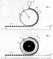
Bei den in
Bei den in
- 1, 1', 1", 1"',1, 1 ', 1 ", 1"',
- Strukturstempelstructure temple
- 11V, 1V 1 1V, 1V
- Strukturstempelstructure temple
- 1o1o
- Rückseiteback
- 22
- Strukturenstructures
- 2o2o
- Prägeflächeembossing surface
- 33
- Prägematerialembossing material
- 3o3o
- erste Seitefirst page
- 3u3u
- zweite Seitesecond page
- 44
- Substrat .Substrate.
- 4o4o
- Zieloberflächetarget surface
- 55
- Porenpore
- 66
- Dispenserdispenser
- 77
- Rotationsachseaxis of rotation
- 88th
- Foliefoil
- 99
- Hohlräumecavities
- 1010
- Erhebungensurveys
- 1111
- Seitenumfangof pages
- 1212
- Abschirmungshielding
- 1414
- Trägercarrier
- 1515
- Hohlraumcavity
- VV
- Geschwindigkeitspeed
Claims (6)
- Method for microcontact embossing of a structure by transfer of an embossing material (3) onto a target surface (4o) of a substrate (4) by means of an embossing surface (2o) of a structural die (1), characterized in that the embossing material (3) consists at least predominantly of silane or at least predominantly of at least one silane derivative or is a molecular component that consists at least predominantly of organic molecules and in that the structural die (1) is a soft die, wherein the structural die (1) is formed in the shape of a roller as a hollow shaft, wherein the cavity in the interior of the hollow shaft is used as a reservoir for the embossing material (3), wherein the structural die (1) has a porous microstructure that consists of pores (5) and that makes possible the passage of the embossing material (3) from the cavity to the surface (2o) of structures (2).
- Method according to Claim 1, in which the molecular component has at least one or more of the structures mentioned below:- Enzymes,- Alkaloids,- Lipids,- Hormones,- Pheromones,- Vitamins,- Carbohydrates,- Peptides,- Nucleic acids,- DNA or DNA strands,- Cells,- Proteins or peptides,- Alkanes, alkenes, alkines, aromatic compounds- Graphene.
- Method according to one of the preceding claims, in which the structural die (1) has an elasticity/a modulus of elasticity of 10-3 MPa and 100 MPa, preferably between 10-2 MPa and 80 MPa, more preferably between 10-1 MPa and 60 MPa, and most preferably between 3 MPa and 40 MPa.
- Method according to one of the preceding claims, in which the structural die (I) is acid-resistant and/or base-resistant.
- Method according to one of the preceding claims, in which the structural die (1) consists at least predominantly, preferably completely, of an inert material.
- Method according to one of the preceding claims, in which the structural die (1) is formed from a polymer, in particular PFPE or PDMS.
Applications Claiming Priority (2)
| Application Number | Priority Date | Filing Date | Title |
|---|---|---|---|
| DE102012112030.7A DE102012112030A1 (en) | 2012-12-10 | 2012-12-10 | Method for microcontact embossing |
| PCT/EP2013/075562 WO2014090661A1 (en) | 2012-12-10 | 2013-12-04 | Method for microcontact printing |
Publications (2)
| Publication Number | Publication Date |
|---|---|
| EP2888629A1 EP2888629A1 (en) | 2015-07-01 |
| EP2888629B1 true EP2888629B1 (en) | 2016-03-02 |
Family
ID=49709685
Family Applications (1)
| Application Number | Title | Priority Date | Filing Date |
|---|---|---|---|
| EP13799316.8A Active EP2888629B1 (en) | 2012-12-10 | 2013-12-04 | Method for microcontact printing |
Country Status (8)
| Country | Link |
|---|---|
| US (1) | US9323144B2 (en) |
| EP (1) | EP2888629B1 (en) |
| JP (1) | JP2016511931A (en) |
| KR (1) | KR101759810B1 (en) |
| CN (2) | CN104823107A (en) |
| DE (1) | DE102012112030A1 (en) |
| SG (1) | SG11201503318PA (en) |
| WO (1) | WO2014090661A1 (en) |
Families Citing this family (11)
| Publication number | Priority date | Publication date | Assignee | Title |
|---|---|---|---|---|
| US11472171B2 (en) * | 2014-07-20 | 2022-10-18 | X Display Company Technology Limited | Apparatus and methods for micro-transfer-printing |
| WO2016070869A2 (en) * | 2014-11-03 | 2016-05-12 | Universität Osnabrück | Device for carrying out a capillary nanoprinting method, a method for carrying out capillary nanoprinting using the device, products obtained according to the method and use of the device |
| CN104356740B (en) * | 2014-11-05 | 2017-05-17 | 广西师范学院 | Method for performing microcontact printing by using water-soluble porphyrin iron complex |
| BR112017013073A2 (en) * | 2014-12-22 | 2018-01-02 | Koninklijke Philips Nv | lithograph stamp, method of making a stamp, use of a stamp, and printing method |
| JP2018520512A (en) * | 2015-06-25 | 2018-07-26 | エーファウ・グループ・エー・タルナー・ゲーエムベーハー | Method for producing a structure on a substrate surface |
| CN106486209A (en) * | 2015-08-31 | 2017-03-08 | 中国科学院宁波材料技术与工程研究所 | A kind of patterning 3D graphene conductive film and its environment-friendly preparation method thereof and application |
| CN105319840A (en) * | 2015-11-23 | 2016-02-10 | 南通天鸿镭射科技有限公司 | Apparatus and method for manufacturing ultraviolet-light-cured seamless-moulded roller wheel through replication technology |
| JP6545401B2 (en) * | 2016-04-06 | 2019-07-17 | コーニンクレッカ フィリップス エヌ ヴェKoninklijke Philips N.V. | Method of making imprint lithography stamp and method of use |
| CN106542494B (en) * | 2016-09-26 | 2017-12-26 | 西北工业大学 | A kind of method for preparing the not contour micro-nano structure of multilayer |
| JP6854733B2 (en) * | 2017-08-17 | 2021-04-07 | 株式会社ジェイエスピー | Resin sheet |
| US20230375759A1 (en) * | 2022-05-18 | 2023-11-23 | GE Precision Healthcare LLC | Aligned and stacked high-aspect ratio metallized structures |
Family Cites Families (23)
| Publication number | Priority date | Publication date | Assignee | Title |
|---|---|---|---|---|
| NL261937A (en) * | 1960-03-16 | 1900-01-01 | ||
| US3678848A (en) * | 1969-08-25 | 1972-07-25 | Weber Marking Systems Inc | Inking pad and use thereof |
| US3709647A (en) * | 1970-10-21 | 1973-01-09 | Clear Pack Co | Apparatus for forming an embossed thermoplastic sheet |
| JPS5436617B2 (en) * | 1973-02-07 | 1979-11-10 | ||
| US3971315A (en) * | 1974-08-12 | 1976-07-27 | Porelon, Inc. | Macroporous microporous marking structure |
| JPH10278217A (en) * | 1997-04-09 | 1998-10-20 | Asahi Optical Co Ltd | Printing plate, its manufacture, and printer using the plate |
| US6276272B1 (en) * | 1996-10-01 | 2001-08-21 | Brother Kogyo Kabushiki Kaisha | Stamp plate producing apparatus for producing stamp plate used in a stamp device |
| US6048623A (en) * | 1996-12-18 | 2000-04-11 | Kimberly-Clark Worldwide, Inc. | Method of contact printing on gold coated films |
| DE19949993C1 (en) * | 1999-10-15 | 2001-05-03 | Peter Barth | Microcontact printing process, for structuring oxidized surfaces using stamp in microelectronics, comprises wetting surface of stamp with silane or thiol molecules before contacting the stamp with oxidized surfaces |
| EP1171800B1 (en) * | 2000-02-07 | 2006-04-19 | Koninklijke Philips Electronics N.V. | Stamp for use in a lithographic process, method of manufacturing a stamp, and method of manufacturing a patterned layer on a substrate |
| JP4278977B2 (en) * | 2000-11-22 | 2009-06-17 | コーニンクレッカ フィリップス エレクトロニクス エヌ ヴィ | Stamp, method and apparatus |
| US6817293B2 (en) * | 2001-03-28 | 2004-11-16 | Dainippon Printing Co., Ltd. | Patterning method with micro-contact printing and its printed product |
| JP5055672B2 (en) * | 2001-07-31 | 2012-10-24 | 大日本印刷株式会社 | Thin film pattern forming stamp |
| US20030127002A1 (en) * | 2002-01-04 | 2003-07-10 | Hougham Gareth Geoffrey | Multilayer architechture for microcontact printing stamps |
| GB0326904D0 (en) * | 2003-11-19 | 2003-12-24 | Koninkl Philips Electronics Nv | Formation of self-assembled monolayers |
| EP1804979A1 (en) * | 2004-10-22 | 2007-07-11 | Koninklijke Philips Electronics N.V. | Roller micro-contact printer with pressure control |
| EP2087403B1 (en) | 2006-11-01 | 2012-02-01 | Koninklijke Philips Electronics N.V. | Imprint method for forming a relief layer and use of it as an etch mask |
| US20080230773A1 (en) | 2007-03-20 | 2008-09-25 | Nano Terra Inc. | Polymer Composition for Preparing Electronic Devices by Microcontact Printing Processes and Products Prepared by the Processes |
| US7959975B2 (en) * | 2007-04-18 | 2011-06-14 | Micron Technology, Inc. | Methods of patterning a substrate |
| WO2010002788A1 (en) | 2008-06-30 | 2010-01-07 | 3M Innovative Properties Company | Solvent assisted method of microcontact printing |
| JP2010171281A (en) * | 2009-01-23 | 2010-08-05 | Jsr Corp | Imprinting method |
| WO2010115027A1 (en) * | 2009-04-01 | 2010-10-07 | Nano Terra Inc. | Methods of patterning substrates using microcontact printed polymer resists and articles prepared therefrom |
| EP2516162A4 (en) * | 2009-12-22 | 2015-10-28 | 3M Innovative Properties Co | Apparatus and method for microcontact printing using a pressurized roller |
-
2012
- 2012-12-10 DE DE102012112030.7A patent/DE102012112030A1/en not_active Ceased
-
2013
- 2013-12-04 CN CN201380064460.4A patent/CN104823107A/en active Pending
- 2013-12-04 KR KR1020157014532A patent/KR101759810B1/en active IP Right Grant
- 2013-12-04 JP JP2015546946A patent/JP2016511931A/en active Pending
- 2013-12-04 WO PCT/EP2013/075562 patent/WO2014090661A1/en active Application Filing
- 2013-12-04 US US14/439,860 patent/US9323144B2/en active Active
- 2013-12-04 EP EP13799316.8A patent/EP2888629B1/en active Active
- 2013-12-04 CN CN201910665524.5A patent/CN110376844A/en active Pending
- 2013-12-04 SG SG11201503318PA patent/SG11201503318PA/en unknown
Also Published As
| Publication number | Publication date |
|---|---|
| CN110376844A (en) | 2019-10-25 |
| SG11201503318PA (en) | 2015-06-29 |
| JP2016511931A (en) | 2016-04-21 |
| CN104823107A (en) | 2015-08-05 |
| EP2888629A1 (en) | 2015-07-01 |
| KR20150092139A (en) | 2015-08-12 |
| US20150293442A1 (en) | 2015-10-15 |
| US9323144B2 (en) | 2016-04-26 |
| WO2014090661A1 (en) | 2014-06-19 |
| DE102012112030A1 (en) | 2014-06-12 |
| KR101759810B1 (en) | 2017-07-19 |
Similar Documents
| Publication | Publication Date | Title |
|---|---|---|
| EP2888629B1 (en) | Method for microcontact printing | |
| Xia et al. | Extending microcontact printing as a microlithographic technique | |
| EP3215895B1 (en) | Method for carrying out capillary nanoprinting, field of ink drops and field of wires obtained according to the method | |
| EP2150854B1 (en) | Die for micro-contact printing and method for the production thereof | |
| DE60310443T2 (en) | PRINTING METHOD WITH RUBBER TEMPLE | |
| EP2870510B1 (en) | Structure stamp, device and method for embossing | |
| EP2329319B1 (en) | Improved nanoimprint method | |
| DE102013216540A1 (en) | Transfer device and molded material | |
| Jang et al. | Agarose‐Assisted Micro‐Contact Printing for High‐Quality Biomolecular Micro‐Patterns | |
| EP1764648B1 (en) | Stamp with nanostructures and device as well as process for its production | |
| DE19935558B4 (en) | Method for producing structures in a substrate in the nanometer range | |
| EP3401731B1 (en) | Stamp with a stamp structure and method for the production of same | |
| DE102004033440A1 (en) | Microstructured device and method for its production | |
| DE102008055960A1 (en) | Method for creation of molds, particularly printing or embossing molds by using multiple nano-gravers, involves embossing nano-graver on surface in recesses, such that male mold is provided | |
| EP3555705B1 (en) | Device and method for producing large-area periodic nanostructures on an extensive substrate by means of a nanoimprint method | |
| EP4176311B1 (en) | Method for producing micro- and/or nano-structures | |
| Kim et al. | In situ curing of sliding SU-8 droplet over a microcontact printed pattern for tunable fabrication of a polydimethylsiloxane nanoslit | |
| DE10207393A1 (en) | Rapid prototyping of miniature plastics components, e.g. for micro-fluid applications, uses a computer-controlled printer to apply a polymer mixture to a carrier in structured layers where polymer components can be removed | |
| EP2771161B1 (en) | Nanoshaping-structure | |
| DE102009018849A1 (en) | Master structure for embossing and/or printing foils in e.g. printing technology for structured application of liquid, has monocrystalline substrate area comprising thickness such that area is formed with curvature radius | |
| WO2022175361A1 (en) | Microfluidic system consisting of a folded foil, and production method | |
| DE102012023514B3 (en) | Device useful for transferring a cell suspension on substrate comprises roller body having a portion of its outer contour, as roll-off surface which is scrollable over the substrate, and a control unit for controlling the contact pressure | |
| DE102017011726A1 (en) | Lamination of polymer layers | |
| WO2008154907A2 (en) | Method and device for transferring nanostructures by means of contact stamping | |
| EP4070160A1 (en) | Method and apparatus for removal of a stamp |
Legal Events
| Date | Code | Title | Description |
|---|---|---|---|
| PUAI | Public reference made under article 153(3) epc to a published international application that has entered the european phase |
Free format text: ORIGINAL CODE: 0009012 |
|
| 17P | Request for examination filed |
Effective date: 20150325 |
|
| AK | Designated contracting states |
Kind code of ref document: A1 Designated state(s): AL AT BE BG CH CY CZ DE DK EE ES FI FR GB GR HR HU IE IS IT LI LT LU LV MC MK MT NL NO PL PT RO RS SE SI SK SM TR |
|
| AX | Request for extension of the european patent |
Extension state: BA ME |
|
| GRAP | Despatch of communication of intention to grant a patent |
Free format text: ORIGINAL CODE: EPIDOSNIGR1 |
|
| GRAJ | Information related to disapproval of communication of intention to grant by the applicant or resumption of examination proceedings by the epo deleted |
Free format text: ORIGINAL CODE: EPIDOSDIGR1 |
|
| GRAP | Despatch of communication of intention to grant a patent |
Free format text: ORIGINAL CODE: EPIDOSNIGR1 |
|
| DAX | Request for extension of the european patent (deleted) | ||
| INTG | Intention to grant announced |
Effective date: 20150918 |
|
| INTG | Intention to grant announced |
Effective date: 20151005 |
|
| GRAS | Grant fee paid |
Free format text: ORIGINAL CODE: EPIDOSNIGR3 |
|
| GRAA | (expected) grant |
Free format text: ORIGINAL CODE: 0009210 |
|
| AK | Designated contracting states |
Kind code of ref document: B1 Designated state(s): AL AT BE BG CH CY CZ DE DK EE ES FI FR GB GR HR HU IE IS IT LI LT LU LV MC MK MT NL NO PL PT RO RS SE SI SK SM TR |
|
| REG | Reference to a national code |
Ref country code: GB Ref legal event code: FG4D Free format text: NOT ENGLISH |
|
| REG | Reference to a national code |
Ref country code: AT Ref legal event code: REF Ref document number: 778435 Country of ref document: AT Kind code of ref document: T Effective date: 20160315 Ref country code: CH Ref legal event code: EP |
|
| REG | Reference to a national code |
Ref country code: IE Ref legal event code: FG4D Free format text: LANGUAGE OF EP DOCUMENT: GERMAN |
|
| REG | Reference to a national code |
Ref country code: DE Ref legal event code: R096 Ref document number: 502013002079 Country of ref document: DE |
|
| REG | Reference to a national code |
Ref country code: NL Ref legal event code: MP Effective date: 20160302 |
|
| REG | Reference to a national code |
Ref country code: LT Ref legal event code: MG4D |
|
| PG25 | Lapsed in a contracting state [announced via postgrant information from national office to epo] |
Ref country code: FI Free format text: LAPSE BECAUSE OF FAILURE TO SUBMIT A TRANSLATION OF THE DESCRIPTION OR TO PAY THE FEE WITHIN THE PRESCRIBED TIME-LIMIT Effective date: 20160302 Ref country code: ES Free format text: LAPSE BECAUSE OF FAILURE TO SUBMIT A TRANSLATION OF THE DESCRIPTION OR TO PAY THE FEE WITHIN THE PRESCRIBED TIME-LIMIT Effective date: 20160302 Ref country code: GR Free format text: LAPSE BECAUSE OF FAILURE TO SUBMIT A TRANSLATION OF THE DESCRIPTION OR TO PAY THE FEE WITHIN THE PRESCRIBED TIME-LIMIT Effective date: 20160603 Ref country code: NO Free format text: LAPSE BECAUSE OF FAILURE TO SUBMIT A TRANSLATION OF THE DESCRIPTION OR TO PAY THE FEE WITHIN THE PRESCRIBED TIME-LIMIT Effective date: 20160602 Ref country code: HR Free format text: LAPSE BECAUSE OF FAILURE TO SUBMIT A TRANSLATION OF THE DESCRIPTION OR TO PAY THE FEE WITHIN THE PRESCRIBED TIME-LIMIT Effective date: 20160302 |
|
| PG25 | Lapsed in a contracting state [announced via postgrant information from national office to epo] |
Ref country code: LV Free format text: LAPSE BECAUSE OF FAILURE TO SUBMIT A TRANSLATION OF THE DESCRIPTION OR TO PAY THE FEE WITHIN THE PRESCRIBED TIME-LIMIT Effective date: 20160302 Ref country code: SE Free format text: LAPSE BECAUSE OF FAILURE TO SUBMIT A TRANSLATION OF THE DESCRIPTION OR TO PAY THE FEE WITHIN THE PRESCRIBED TIME-LIMIT Effective date: 20160302 Ref country code: PL Free format text: LAPSE BECAUSE OF FAILURE TO SUBMIT A TRANSLATION OF THE DESCRIPTION OR TO PAY THE FEE WITHIN THE PRESCRIBED TIME-LIMIT Effective date: 20160302 Ref country code: NL Free format text: LAPSE BECAUSE OF FAILURE TO SUBMIT A TRANSLATION OF THE DESCRIPTION OR TO PAY THE FEE WITHIN THE PRESCRIBED TIME-LIMIT Effective date: 20160302 Ref country code: LT Free format text: LAPSE BECAUSE OF FAILURE TO SUBMIT A TRANSLATION OF THE DESCRIPTION OR TO PAY THE FEE WITHIN THE PRESCRIBED TIME-LIMIT Effective date: 20160302 Ref country code: RS Free format text: LAPSE BECAUSE OF FAILURE TO SUBMIT A TRANSLATION OF THE DESCRIPTION OR TO PAY THE FEE WITHIN THE PRESCRIBED TIME-LIMIT Effective date: 20160302 |
|
| PG25 | Lapsed in a contracting state [announced via postgrant information from national office to epo] |
Ref country code: EE Free format text: LAPSE BECAUSE OF FAILURE TO SUBMIT A TRANSLATION OF THE DESCRIPTION OR TO PAY THE FEE WITHIN THE PRESCRIBED TIME-LIMIT Effective date: 20160302 Ref country code: IS Free format text: LAPSE BECAUSE OF FAILURE TO SUBMIT A TRANSLATION OF THE DESCRIPTION OR TO PAY THE FEE WITHIN THE PRESCRIBED TIME-LIMIT Effective date: 20160702 |
|
| PG25 | Lapsed in a contracting state [announced via postgrant information from national office to epo] |
Ref country code: SM Free format text: LAPSE BECAUSE OF FAILURE TO SUBMIT A TRANSLATION OF THE DESCRIPTION OR TO PAY THE FEE WITHIN THE PRESCRIBED TIME-LIMIT Effective date: 20160302 Ref country code: PT Free format text: LAPSE BECAUSE OF FAILURE TO SUBMIT A TRANSLATION OF THE DESCRIPTION OR TO PAY THE FEE WITHIN THE PRESCRIBED TIME-LIMIT Effective date: 20160704 Ref country code: CZ Free format text: LAPSE BECAUSE OF FAILURE TO SUBMIT A TRANSLATION OF THE DESCRIPTION OR TO PAY THE FEE WITHIN THE PRESCRIBED TIME-LIMIT Effective date: 20160302 Ref country code: SK Free format text: LAPSE BECAUSE OF FAILURE TO SUBMIT A TRANSLATION OF THE DESCRIPTION OR TO PAY THE FEE WITHIN THE PRESCRIBED TIME-LIMIT Effective date: 20160302 Ref country code: RO Free format text: LAPSE BECAUSE OF FAILURE TO SUBMIT A TRANSLATION OF THE DESCRIPTION OR TO PAY THE FEE WITHIN THE PRESCRIBED TIME-LIMIT Effective date: 20160302 |
|
| REG | Reference to a national code |
Ref country code: DE Ref legal event code: R097 Ref document number: 502013002079 Country of ref document: DE |
|
| PG25 | Lapsed in a contracting state [announced via postgrant information from national office to epo] |
Ref country code: IT Free format text: LAPSE BECAUSE OF FAILURE TO SUBMIT A TRANSLATION OF THE DESCRIPTION OR TO PAY THE FEE WITHIN THE PRESCRIBED TIME-LIMIT Effective date: 20160302 |
|
| PLBE | No opposition filed within time limit |
Free format text: ORIGINAL CODE: 0009261 |
|
| STAA | Information on the status of an ep patent application or granted ep patent |
Free format text: STATUS: NO OPPOSITION FILED WITHIN TIME LIMIT |
|
| PG25 | Lapsed in a contracting state [announced via postgrant information from national office to epo] |
Ref country code: DK Free format text: LAPSE BECAUSE OF FAILURE TO SUBMIT A TRANSLATION OF THE DESCRIPTION OR TO PAY THE FEE WITHIN THE PRESCRIBED TIME-LIMIT Effective date: 20160302 |
|
| 26N | No opposition filed |
Effective date: 20161205 |
|
| PG25 | Lapsed in a contracting state [announced via postgrant information from national office to epo] |
Ref country code: BG Free format text: LAPSE BECAUSE OF FAILURE TO SUBMIT A TRANSLATION OF THE DESCRIPTION OR TO PAY THE FEE WITHIN THE PRESCRIBED TIME-LIMIT Effective date: 20160602 Ref country code: SI Free format text: LAPSE BECAUSE OF FAILURE TO SUBMIT A TRANSLATION OF THE DESCRIPTION OR TO PAY THE FEE WITHIN THE PRESCRIBED TIME-LIMIT Effective date: 20160302 |
|
| PG25 | Lapsed in a contracting state [announced via postgrant information from national office to epo] |
Ref country code: BE Free format text: LAPSE BECAUSE OF NON-PAYMENT OF DUE FEES Effective date: 20161231 |
|
| REG | Reference to a national code |
Ref country code: CH Ref legal event code: PL |
|
| PG25 | Lapsed in a contracting state [announced via postgrant information from national office to epo] |
Ref country code: MC Free format text: LAPSE BECAUSE OF FAILURE TO SUBMIT A TRANSLATION OF THE DESCRIPTION OR TO PAY THE FEE WITHIN THE PRESCRIBED TIME-LIMIT Effective date: 20160302 |
|
| REG | Reference to a national code |
Ref country code: FR Ref legal event code: ST Effective date: 20170831 |
|
| REG | Reference to a national code |
Ref country code: IE Ref legal event code: MM4A |
|
| PG25 | Lapsed in a contracting state [announced via postgrant information from national office to epo] |
Ref country code: CH Free format text: LAPSE BECAUSE OF NON-PAYMENT OF DUE FEES Effective date: 20161231 Ref country code: LU Free format text: LAPSE BECAUSE OF NON-PAYMENT OF DUE FEES Effective date: 20161204 Ref country code: LI Free format text: LAPSE BECAUSE OF NON-PAYMENT OF DUE FEES Effective date: 20161231 Ref country code: FR Free format text: LAPSE BECAUSE OF NON-PAYMENT OF DUE FEES Effective date: 20170102 |
|
| PG25 | Lapsed in a contracting state [announced via postgrant information from national office to epo] |
Ref country code: IE Free format text: LAPSE BECAUSE OF NON-PAYMENT OF DUE FEES Effective date: 20161204 |
|
| REG | Reference to a national code |
Ref country code: BE Ref legal event code: MM Effective date: 20161231 |
|
| PG25 | Lapsed in a contracting state [announced via postgrant information from national office to epo] |
Ref country code: HU Free format text: LAPSE BECAUSE OF FAILURE TO SUBMIT A TRANSLATION OF THE DESCRIPTION OR TO PAY THE FEE WITHIN THE PRESCRIBED TIME-LIMIT; INVALID AB INITIO Effective date: 20131204 |
|
| PG25 | Lapsed in a contracting state [announced via postgrant information from national office to epo] |
Ref country code: MK Free format text: LAPSE BECAUSE OF FAILURE TO SUBMIT A TRANSLATION OF THE DESCRIPTION OR TO PAY THE FEE WITHIN THE PRESCRIBED TIME-LIMIT Effective date: 20160302 Ref country code: CY Free format text: LAPSE BECAUSE OF FAILURE TO SUBMIT A TRANSLATION OF THE DESCRIPTION OR TO PAY THE FEE WITHIN THE PRESCRIBED TIME-LIMIT Effective date: 20160302 |
|
| GBPC | Gb: european patent ceased through non-payment of renewal fee |
Effective date: 20171204 |
|
| PG25 | Lapsed in a contracting state [announced via postgrant information from national office to epo] |
Ref country code: MT Free format text: LAPSE BECAUSE OF FAILURE TO SUBMIT A TRANSLATION OF THE DESCRIPTION OR TO PAY THE FEE WITHIN THE PRESCRIBED TIME-LIMIT Effective date: 20160302 |
|
| PG25 | Lapsed in a contracting state [announced via postgrant information from national office to epo] |
Ref country code: AL Free format text: LAPSE BECAUSE OF FAILURE TO SUBMIT A TRANSLATION OF THE DESCRIPTION OR TO PAY THE FEE WITHIN THE PRESCRIBED TIME-LIMIT Effective date: 20160302 Ref country code: TR Free format text: LAPSE BECAUSE OF FAILURE TO SUBMIT A TRANSLATION OF THE DESCRIPTION OR TO PAY THE FEE WITHIN THE PRESCRIBED TIME-LIMIT Effective date: 20160302 |
|
| PG25 | Lapsed in a contracting state [announced via postgrant information from national office to epo] |
Ref country code: GB Free format text: LAPSE BECAUSE OF NON-PAYMENT OF DUE FEES Effective date: 20171204 |
|
| PGFP | Annual fee paid to national office [announced via postgrant information from national office to epo] |
Ref country code: DE Payment date: 20231214 Year of fee payment: 11 Ref country code: AT Payment date: 20231214 Year of fee payment: 11 |