EP2887393A2 - Nachgiebige dielektrische Schicht für ein Halbleiterbauelement - Google Patents
Nachgiebige dielektrische Schicht für ein Halbleiterbauelement Download PDFInfo
- Publication number
- EP2887393A2 EP2887393A2 EP14004185.6A EP14004185A EP2887393A2 EP 2887393 A2 EP2887393 A2 EP 2887393A2 EP 14004185 A EP14004185 A EP 14004185A EP 2887393 A2 EP2887393 A2 EP 2887393A2
- Authority
- EP
- European Patent Office
- Prior art keywords
- compliant dielectric
- layer
- dielectric material
- electrically conductive
- semiconductor material
- Prior art date
- Legal status (The legal status is an assumption and is not a legal conclusion. Google has not performed a legal analysis and makes no representation as to the accuracy of the status listed.)
- Withdrawn
Links
Images





Classifications
-
- H—ELECTRICITY
- H10—SEMICONDUCTOR DEVICES; ELECTRIC SOLID-STATE DEVICES NOT OTHERWISE PROVIDED FOR
- H10W—GENERIC PACKAGES, INTERCONNECTIONS, CONNECTORS OR OTHER CONSTRUCTIONAL DETAILS OF DEVICES COVERED BY CLASS H10
- H10W90/00—Package configurations
-
- H—ELECTRICITY
- H10—SEMICONDUCTOR DEVICES; ELECTRIC SOLID-STATE DEVICES NOT OTHERWISE PROVIDED FOR
- H10W—GENERIC PACKAGES, INTERCONNECTIONS, CONNECTORS OR OTHER CONSTRUCTIONAL DETAILS OF DEVICES COVERED BY CLASS H10
- H10W20/00—Interconnections in chips, wafers or substrates
- H10W20/01—Manufacture or treatment
-
- H—ELECTRICITY
- H10—SEMICONDUCTOR DEVICES; ELECTRIC SOLID-STATE DEVICES NOT OTHERWISE PROVIDED FOR
- H10W—GENERIC PACKAGES, INTERCONNECTIONS, CONNECTORS OR OTHER CONSTRUCTIONAL DETAILS OF DEVICES COVERED BY CLASS H10
- H10W20/00—Interconnections in chips, wafers or substrates
- H10W20/01—Manufacture or treatment
- H10W20/021—Manufacture or treatment of interconnections within wafers or substrates
- H10W20/023—Manufacture or treatment of interconnections within wafers or substrates the interconnections being through-semiconductor vias
-
- H—ELECTRICITY
- H10—SEMICONDUCTOR DEVICES; ELECTRIC SOLID-STATE DEVICES NOT OTHERWISE PROVIDED FOR
- H10W—GENERIC PACKAGES, INTERCONNECTIONS, CONNECTORS OR OTHER CONSTRUCTIONAL DETAILS OF DEVICES COVERED BY CLASS H10
- H10W20/00—Interconnections in chips, wafers or substrates
- H10W20/01—Manufacture or treatment
- H10W20/021—Manufacture or treatment of interconnections within wafers or substrates
- H10W20/023—Manufacture or treatment of interconnections within wafers or substrates the interconnections being through-semiconductor vias
- H10W20/0245—Manufacture or treatment of interconnections within wafers or substrates the interconnections being through-semiconductor vias comprising use of blind vias during the manufacture
-
- H—ELECTRICITY
- H10—SEMICONDUCTOR DEVICES; ELECTRIC SOLID-STATE DEVICES NOT OTHERWISE PROVIDED FOR
- H10W—GENERIC PACKAGES, INTERCONNECTIONS, CONNECTORS OR OTHER CONSTRUCTIONAL DETAILS OF DEVICES COVERED BY CLASS H10
- H10W20/00—Interconnections in chips, wafers or substrates
- H10W20/01—Manufacture or treatment
- H10W20/021—Manufacture or treatment of interconnections within wafers or substrates
- H10W20/023—Manufacture or treatment of interconnections within wafers or substrates the interconnections being through-semiconductor vias
- H10W20/0249—Manufacture or treatment of interconnections within wafers or substrates the interconnections being through-semiconductor vias wherein the through-semiconductor via protrudes from backsides of the chips, wafers or substrates during the manufacture
-
- H—ELECTRICITY
- H10—SEMICONDUCTOR DEVICES; ELECTRIC SOLID-STATE DEVICES NOT OTHERWISE PROVIDED FOR
- H10W—GENERIC PACKAGES, INTERCONNECTIONS, CONNECTORS OR OTHER CONSTRUCTIONAL DETAILS OF DEVICES COVERED BY CLASS H10
- H10W20/00—Interconnections in chips, wafers or substrates
- H10W20/20—Interconnections within wafers or substrates, e.g. through-silicon vias [TSV]
-
- H—ELECTRICITY
- H10—SEMICONDUCTOR DEVICES; ELECTRIC SOLID-STATE DEVICES NOT OTHERWISE PROVIDED FOR
- H10W—GENERIC PACKAGES, INTERCONNECTIONS, CONNECTORS OR OTHER CONSTRUCTIONAL DETAILS OF DEVICES COVERED BY CLASS H10
- H10W20/00—Interconnections in chips, wafers or substrates
- H10W20/40—Interconnections external to wafers or substrates, e.g. back-end-of-line [BEOL] metallisations or vias connecting to gate electrodes
- H10W20/41—Interconnections external to wafers or substrates, e.g. back-end-of-line [BEOL] metallisations or vias connecting to gate electrodes characterised by their conductive parts
- H10W20/43—Layouts of interconnections
-
- H—ELECTRICITY
- H10—SEMICONDUCTOR DEVICES; ELECTRIC SOLID-STATE DEVICES NOT OTHERWISE PROVIDED FOR
- H10W—GENERIC PACKAGES, INTERCONNECTIONS, CONNECTORS OR OTHER CONSTRUCTIONAL DETAILS OF DEVICES COVERED BY CLASS H10
- H10W70/00—Package substrates; Interposers; Redistribution layers [RDL]
- H10W70/01—Manufacture or treatment
- H10W70/04—Manufacture or treatment of leadframes
- H10W70/042—Etching
-
- H—ELECTRICITY
- H10—SEMICONDUCTOR DEVICES; ELECTRIC SOLID-STATE DEVICES NOT OTHERWISE PROVIDED FOR
- H10W—GENERIC PACKAGES, INTERCONNECTIONS, CONNECTORS OR OTHER CONSTRUCTIONAL DETAILS OF DEVICES COVERED BY CLASS H10
- H10W70/00—Package substrates; Interposers; Redistribution layers [RDL]
- H10W70/01—Manufacture or treatment
- H10W70/05—Manufacture or treatment of insulating or insulated package substrates, or of interposers, or of redistribution layers
- H10W70/095—Manufacture or treatment of insulating or insulated package substrates, or of interposers, or of redistribution layers of vias therein
-
- H—ELECTRICITY
- H10—SEMICONDUCTOR DEVICES; ELECTRIC SOLID-STATE DEVICES NOT OTHERWISE PROVIDED FOR
- H10W—GENERIC PACKAGES, INTERCONNECTIONS, CONNECTORS OR OTHER CONSTRUCTIONAL DETAILS OF DEVICES COVERED BY CLASS H10
- H10W70/00—Package substrates; Interposers; Redistribution layers [RDL]
- H10W70/099—Connecting interconnections to insulating or insulated package substrates, interposers or redistribution layers
-
- H—ELECTRICITY
- H10—SEMICONDUCTOR DEVICES; ELECTRIC SOLID-STATE DEVICES NOT OTHERWISE PROVIDED FOR
- H10W—GENERIC PACKAGES, INTERCONNECTIONS, CONNECTORS OR OTHER CONSTRUCTIONAL DETAILS OF DEVICES COVERED BY CLASS H10
- H10W70/00—Package substrates; Interposers; Redistribution layers [RDL]
- H10W70/60—Insulating or insulated package substrates; Interposers; Redistribution layers
- H10W70/62—Insulating or insulated package substrates; Interposers; Redistribution layers characterised by their interconnections
- H10W70/63—Vias, e.g. via plugs
- H10W70/635—Through-vias
-
- H—ELECTRICITY
- H10—SEMICONDUCTOR DEVICES; ELECTRIC SOLID-STATE DEVICES NOT OTHERWISE PROVIDED FOR
- H10W—GENERIC PACKAGES, INTERCONNECTIONS, CONNECTORS OR OTHER CONSTRUCTIONAL DETAILS OF DEVICES COVERED BY CLASS H10
- H10W70/00—Package substrates; Interposers; Redistribution layers [RDL]
- H10W70/60—Insulating or insulated package substrates; Interposers; Redistribution layers
- H10W70/62—Insulating or insulated package substrates; Interposers; Redistribution layers characterised by their interconnections
- H10W70/65—Shapes or dispositions of interconnections
-
- H—ELECTRICITY
- H10—SEMICONDUCTOR DEVICES; ELECTRIC SOLID-STATE DEVICES NOT OTHERWISE PROVIDED FOR
- H10W—GENERIC PACKAGES, INTERCONNECTIONS, CONNECTORS OR OTHER CONSTRUCTIONAL DETAILS OF DEVICES COVERED BY CLASS H10
- H10W72/00—Interconnections or connectors in packages
-
- H—ELECTRICITY
- H10—SEMICONDUCTOR DEVICES; ELECTRIC SOLID-STATE DEVICES NOT OTHERWISE PROVIDED FOR
- H10W—GENERIC PACKAGES, INTERCONNECTIONS, CONNECTORS OR OTHER CONSTRUCTIONAL DETAILS OF DEVICES COVERED BY CLASS H10
- H10W74/00—Encapsulations, e.g. protective coatings
- H10W74/10—Encapsulations, e.g. protective coatings characterised by their shape or disposition
- H10W74/131—Encapsulations, e.g. protective coatings characterised by their shape or disposition the semiconductor body being only partially enclosed
- H10W74/137—Encapsulations, e.g. protective coatings characterised by their shape or disposition the semiconductor body being only partially enclosed the encapsulations being directly on the semiconductor body
-
- H—ELECTRICITY
- H10—SEMICONDUCTOR DEVICES; ELECTRIC SOLID-STATE DEVICES NOT OTHERWISE PROVIDED FOR
- H10W—GENERIC PACKAGES, INTERCONNECTIONS, CONNECTORS OR OTHER CONSTRUCTIONAL DETAILS OF DEVICES COVERED BY CLASS H10
- H10W74/00—Encapsulations, e.g. protective coatings
- H10W74/10—Encapsulations, e.g. protective coatings characterised by their shape or disposition
- H10W74/131—Encapsulations, e.g. protective coatings characterised by their shape or disposition the semiconductor body being only partially enclosed
- H10W74/147—Encapsulations, e.g. protective coatings characterised by their shape or disposition the semiconductor body being only partially enclosed the encapsulations being multilayered
-
- H—ELECTRICITY
- H10—SEMICONDUCTOR DEVICES; ELECTRIC SOLID-STATE DEVICES NOT OTHERWISE PROVIDED FOR
- H10W—GENERIC PACKAGES, INTERCONNECTIONS, CONNECTORS OR OTHER CONSTRUCTIONAL DETAILS OF DEVICES COVERED BY CLASS H10
- H10W72/00—Interconnections or connectors in packages
- H10W72/01—Manufacture or treatment
- H10W72/019—Manufacture or treatment of bond pads
- H10W72/01931—Manufacture or treatment of bond pads using blanket deposition
- H10W72/01933—Manufacture or treatment of bond pads using blanket deposition in liquid form, e.g. spin coating, spray coating or immersion coating
- H10W72/01935—Manufacture or treatment of bond pads using blanket deposition in liquid form, e.g. spin coating, spray coating or immersion coating by plating, e.g. electroless plating or electroplating
-
- H—ELECTRICITY
- H10—SEMICONDUCTOR DEVICES; ELECTRIC SOLID-STATE DEVICES NOT OTHERWISE PROVIDED FOR
- H10W—GENERIC PACKAGES, INTERCONNECTIONS, CONNECTORS OR OTHER CONSTRUCTIONAL DETAILS OF DEVICES COVERED BY CLASS H10
- H10W72/00—Interconnections or connectors in packages
- H10W72/01—Manufacture or treatment
- H10W72/019—Manufacture or treatment of bond pads
- H10W72/01931—Manufacture or treatment of bond pads using blanket deposition
- H10W72/01938—Manufacture or treatment of bond pads using blanket deposition in gaseous form, e.g. by CVD or PVD
-
- H—ELECTRICITY
- H10—SEMICONDUCTOR DEVICES; ELECTRIC SOLID-STATE DEVICES NOT OTHERWISE PROVIDED FOR
- H10W—GENERIC PACKAGES, INTERCONNECTIONS, CONNECTORS OR OTHER CONSTRUCTIONAL DETAILS OF DEVICES COVERED BY CLASS H10
- H10W72/00—Interconnections or connectors in packages
- H10W72/20—Bump connectors, e.g. solder bumps or copper pillars; Dummy bumps; Thermal bumps
-
- H—ELECTRICITY
- H10—SEMICONDUCTOR DEVICES; ELECTRIC SOLID-STATE DEVICES NOT OTHERWISE PROVIDED FOR
- H10W—GENERIC PACKAGES, INTERCONNECTIONS, CONNECTORS OR OTHER CONSTRUCTIONAL DETAILS OF DEVICES COVERED BY CLASS H10
- H10W72/00—Interconnections or connectors in packages
- H10W72/90—Bond pads, in general
- H10W72/941—Dispositions of bond pads
- H10W72/9415—Dispositions of bond pads relative to the surface, e.g. recessed, protruding
-
- H—ELECTRICITY
- H10—SEMICONDUCTOR DEVICES; ELECTRIC SOLID-STATE DEVICES NOT OTHERWISE PROVIDED FOR
- H10W—GENERIC PACKAGES, INTERCONNECTIONS, CONNECTORS OR OTHER CONSTRUCTIONAL DETAILS OF DEVICES COVERED BY CLASS H10
- H10W72/00—Interconnections or connectors in packages
- H10W72/90—Bond pads, in general
- H10W72/951—Materials of bond pads
- H10W72/952—Materials of bond pads comprising metals or metalloids, e.g. PbSn, Ag or Cu
-
- H—ELECTRICITY
- H10—SEMICONDUCTOR DEVICES; ELECTRIC SOLID-STATE DEVICES NOT OTHERWISE PROVIDED FOR
- H10W—GENERIC PACKAGES, INTERCONNECTIONS, CONNECTORS OR OTHER CONSTRUCTIONAL DETAILS OF DEVICES COVERED BY CLASS H10
- H10W74/00—Encapsulations, e.g. protective coatings
- H10W74/10—Encapsulations, e.g. protective coatings characterised by their shape or disposition
- H10W74/15—Encapsulations, e.g. protective coatings characterised by their shape or disposition on active surfaces of flip-chip devices, e.g. underfills
-
- H—ELECTRICITY
- H10—SEMICONDUCTOR DEVICES; ELECTRIC SOLID-STATE DEVICES NOT OTHERWISE PROVIDED FOR
- H10W—GENERIC PACKAGES, INTERCONNECTIONS, CONNECTORS OR OTHER CONSTRUCTIONAL DETAILS OF DEVICES COVERED BY CLASS H10
- H10W90/00—Package configurations
- H10W90/701—Package configurations characterised by the relative positions of pads or connectors relative to package parts
- H10W90/721—Package configurations characterised by the relative positions of pads or connectors relative to package parts of bump connectors
- H10W90/722—Package configurations characterised by the relative positions of pads or connectors relative to package parts of bump connectors between stacked chips
-
- H—ELECTRICITY
- H10—SEMICONDUCTOR DEVICES; ELECTRIC SOLID-STATE DEVICES NOT OTHERWISE PROVIDED FOR
- H10W—GENERIC PACKAGES, INTERCONNECTIONS, CONNECTORS OR OTHER CONSTRUCTIONAL DETAILS OF DEVICES COVERED BY CLASS H10
- H10W90/00—Package configurations
- H10W90/701—Package configurations characterised by the relative positions of pads or connectors relative to package parts
- H10W90/721—Package configurations characterised by the relative positions of pads or connectors relative to package parts of bump connectors
- H10W90/724—Package configurations characterised by the relative positions of pads or connectors relative to package parts of bump connectors between a chip and a stacked insulating package substrate, interposer or RDL
Definitions
- the subject matter described herein relates to systems, apparatuses, and methods for compliant dielectric layers for semiconductor devices.
- An integrated circuit is a common element of electronic devices.
- An IC typically includes a die (or chip), upon which electrical circuits are formed, and a package that houses the die.
- Various types of IC packages currently exist.
- wafer level packages exist that are basically dies cut from wafers that have interconnects (e.g., solder bumps) mounted directly thereto.
- the solder bumps are spaced out on the dies by redistribution layers (RDLs) to enable the solder bumps to be directly mounted.
- RDLs redistribution layers
- the solder bumps enable the wafer level packages to be mounted to circuit boards and the like.
- Another type of IC package includes an interposer to which an IC die is mounted. Such a package may be considered another type of wafer level package.
- the interposer is made of a semiconductor material (e.g., silicon) and includes electrically conductive routing and vias, such as through silicon vias (TSVs), and may be referred to as a through silicon via interposer (TSI).
- TSVs through silicon vias
- TSI through silicon via interposer
- the electrically conductive routing traces and vias of the interposer are used to spread out and route signals of the IC die, which is attached to a first surface of the interposer, to interconnects (e.g., solder bumps) on the second, opposing surface of the interposer.
- the interconnects are used to mount the interposer-enabled package to a circuit board.
- such packages undergo temperature cycles (e.g., heating and cooling), which causes thermal expansion of the semiconductor material of the die in a wafer level package, and of the die and interposer in an interposer-enabled wafer level package.
- temperature cycles e.g., heating and cooling
- Such expansion, or enlarging of the area of the die or interposer can cause mechanical stress on the semiconductor material and/or on a passivation layer on the semiconductor material and/or on solder bumps/balls and/or on under bump metallization (UBM) layers (i.e., layers that interface a solder ball/bump with the semiconductor material terminals).
- UBM under bump metallization
- an integrated circuit (IC) package comprising:
- the semiconductor material body includes an active integrated circuit.
- the semiconductor material body is configured as an interposer for the IC package, and the IC package further comprises:
- the IC package further comprises:
- the compliant dielectric material layer comprises:
- At least two of the compliant dielectric material sub-layers comprise different dielectric materials from each other.
- the IC package is configured to be attached to a circuit board using the interconnect member, and wherein the compliant dielectric material layer has a coefficient of thermal expansion that is approximately the same as at least one of the circuit board.
- a method comprises:
- the method further comprises:
- the method further comprises:
- said applying a compliant dielectric material comprises:
- said applying a plurality of compliant dielectric material sub-layers comprises:
- the method further comprises, forming an interconnect member in electrical contact with the second electrically conductive feature; and coupling the interconnect member to a circuit board.
- the method further comprises:
- an integrated circuit (IC) package comprises:
- the IC package further comprises:
- the first electrically conductive via electrically couples the first electrically conductive feature to the third electrically conductive feature
- the second electrically conductive via electrically couples the second electrically conductive feature to the fourth electrically conductive feature
- a first IC die is coupled to the first interconnect member and a second IC die of is coupled to the second interconnect member, and wherein the third interconnect member and the fourth interconnect member are each coupled to a circuit board.
- the compliant dielectric material has a coefficient of thermal expansion property that is approximately equal to a coefficient of thermal expansion property of the circuit board.
- the compliant dielectric material enables the first surface of the through silicon via interposer to have an area of at least 625mm 2 .
- references in the specification to "one embodiment,” “an embodiment,” “an example embodiment,” etc., indicate that the embodiment described may include a particular feature, structure, or characteristic, but every embodiment may not necessarily include the particular feature, structure, or characteristic. Moreover, such phrases are not necessarily referring to the same embodiment. Further, when a particular feature, structure, or characteristic is described in connection with an embodiment, it is submitted that it is within the knowledge of one skilled in the art to affect such feature, structure, or characteristic in connection with other embodiments whether or not explicitly described.
- Coupled and “connected” may refer to physical, operative, electrical, communicative and/or other connections between components described herein, as would be understood by a person of skill in the relevant art(s) having the benefit of this disclosure.
- the embodiments described herein may be adapted to integrated circuit (IC) packaging and to semiconductor devices (e.g., integrated circuit chips and/or dies and semiconductor interposers) which may be used in various types of computing systems, communications systems, communication devices, electronic devices, and/or the like.
- IC integrated circuit
- semiconductor devices e.g., integrated circuit chips and/or dies and semiconductor interposers
- the described embodiments may refer to particular types of packages and devices, although the inventive techniques provided herein may be applicable to other types of packages and devices not explicitly mentioned.
- additional structural and operational embodiments, including modifications and/or alterations will become apparent to persons skilled in the relevant art(s) from the teachings herein.
- a layer of a compliant dielectric material i.e., an organic and/or a non-electrically conductive dielectric material
- a compliant dielectric material i.e., an organic and/or a non-electrically conductive dielectric material
- Electrically conductive vias are formed through the compliant dielectric material to conduct signals from circuits on the IC die to solder balls/bumps.
- the solder balls/bumps are configured to electrically and physically connect the IC die and/or the interposer to an organic substrate or printed circuit board (PCB).
- the compliant dielectric material enables lateral movement and/or compliance during thermal expansion and/or cycling of the die and/or interposer, which reduces or eliminates thermal/mechanical stresses, cracking, detachment, circuit damage, etc., and increases yield, while enabling larger die and interposer sizes (e.g., components with larger areas).
- the compliant dielectric material allows portions of the IC package to expand and/or contract with the PCB during thermal variations. Additionally, mechanical shocks (e.g., during drop tests) are reduced as some energy from impact is absorbed by the organic, compliant dielectric material.
- a compliant dielectric material may be selected based on a coefficient of thermal expansion (CTE) associated with the compliant dielectric material.
- CTE coefficient of thermal expansion
- a compliant dielectric material may be selected based, in whole or in part, on it having a CTE that is equal to or approximately equal to a CTE of the organic substrate and/or the PCB.
- a thickness of a compliant dielectric material applied to an IC package may also be determined based on the CTE of the compliant dielectric material as well as the thermal requirements and/or environment in which the IC package is assembled, tested, and/or operated.
- the thickness of the compliant dielectric layer may be selected such that the overall backside dielectric layer thickness (including compliant dielectric material) is 10 times greater than conventional backside dielectric layer.
- a thick compliant dielectric layer may have a thickness between 10-50 ⁇ m.
- An IC package may be assembled in a manner that utilizes compliant dielectric materials, layers, and/or sub-layers.
- Suitable organic dielectric materials include, without limitation: elastomers, molding compound, Polyimide, Polybenzoxazole (PBO), benzocyclobutene, polytetrafluoroethylene (PTFE), and/or the like.
- Multiple layers (e.g., sub-layers) of compliant dielectric material may be used in a single IC package. Such sub-layers may be deposited on top of each other during assembly using the same process and/or mask, or a different process.
- a semiconductor device includes a semiconductor material body, a compliant dielectric material layer, a first electrically conductive feature, a second electrically conductive feature, an electrically conductive via, and an interconnect member.
- the semiconductor material body has opposing first and second surfaces, and includes the first electrically conductive feature at the first surface.
- the compliant dielectric material layer has opposing first and second surfaces. The first surface of the compliant dielectric material layer is on the second surface of the semiconductor material body, and the compliant dielectric material layer has a deformability that is greater than a deformability of the semiconductor material body.
- the second electrically conductive feature is formed on the second surface of the compliant dielectric material layer.
- the electrically conductive via is formed through the semiconductor material body and the compliant dielectric material layer, and electrically couples the first electrically conductive feature to the second electrically conductive feature.
- the interconnect member is coupled to the second surface of the compliant dielectric material layer and is in electrical contact with the second electrically conductive feature.
- a method in another example aspect, includes forming an opening in a semiconductor material body having opposing first and second surfaces, the opening formed in the first surface of the semiconductor material body.
- the method also includes filling the opening with an electrically conductive material, and forming a first electrically conductive feature on the first surface of the semiconductor material body that is electrically coupled to the electrically conductive material in the filled opening.
- the method further includes applying a support structure to the first surface of the semiconductor material body.
- the method further includes etching the second surface of the semiconductor material body to expose the filled opening as a pillar extending from the second surface of the semiconductor material body.
- the method still further includes applying a compliant dielectric material to the etched second surface of the semiconductor material body and surrounding the pillar (e.g., coating/covering the cylindrical outer surface of the pillar) to form a compliant dielectric material layer, the compliant dielectric material layer having opposing first and second surfaces, the first surface of the compliant dielectric material layer adhering to the second surface of the semiconductor material body.
- the method includes forming a second electrically conductive feature on the second surface of the compliant dielectric material layer in electrical contact with the pillar at the second surface of the compliant dielectric material layer, the pillar being an electrically conductive via through the semiconductor material body and the compliant dielectric material layer.
- an IC package in yet another example aspect, includes a through silicon via interposer having opposing first and second surfaces, and at least one IC die mounted to the first surface of the interposer.
- the interposer includes a semiconductor material body having opposing first and second surfaces, a compliant dielectric material layer having opposing first and second surfaces, a first electrically conductive via, and a second electrically conductive via.
- the first surface of the compliant dielectric material layer is on the second surface of the semiconductor material body, and the compliant dielectric material layer has a deformability that is greater than a deformability of the semiconductor material body.
- the first electrically conductive via and the second electrically conductive via are each formed through the semiconductor material body and the compliant dielectric material layer.
- example embodiments are described in the following subsections. In particular, example embodiments for semiconductor devices and IC packages with compliant dielectric material layers are described, followed by example embodiments for multi-layer compliant dielectric materials. This is followed by a description of example assembly embodiments. Next, further example embodiments and advantages are described. Finally, some concluding remarks are provided.
- a semiconductor device is formed that may be included in an integrated circuit (IC) package.
- the semiconductor device includes one or more through-silicon vias through the semiconductor device to route signals through the semiconductor device.
- the semiconductor device further includes at least one compliant dielectric layer to provide compliance or "flex" during heating/cooling, which reduces package damage/failures that may otherwise occur due to the resulting expansion or contraction.
- the semiconductor device may be an interposer incorporated into an IC package and used to route signals from an attached die to solder balls/bumps of the semiconductor device, and/or the semiconductor device may be an IC package in itself by including active integrated circuits in the semiconductor device.
- FIG. 1 shows a cross-sectional view of a portion of an exemplary semiconductor device 100 that includes a compliant dielectric layer 112, according to an embodiment.
- Semiconductor device 100 includes a first dielectric layer 102, a first metal layer 104, a liner layer 106, a silicon layer 108, a passivation layer 110, compliant dielectric layer 112, a through silicon via 114, a second dielectric layer 116, a second metal layer 118, a connector 120, and a solder ball/bump 122.
- Semiconductor device 100 and each of the components included therein may include functionality and connectivity beyond what is shown in FIG. 1 , as would be apparent to persons skilled in relevant art(s). However, such additional functionality is not shown in FIG. 1 for the sake of brevity.
- First dielectric layer 102 may be part of a top layer of semiconductor device 100.
- first metal layer 104 may also be part of the top layer of semiconductor device 100.
- first metal layer 104 may include one or more redistribution layers (also referred to as redistribution routing, redistribution interconnects, fan-in or fan-out routing, etc.) for signal routing.
- First dielectric layer 102 and first metal layer 104 may be formed on a top surface of silicon layer 108 (i.e., a semiconductor material body), as shown in FIG. 1 , and liner layer 106 may be formed between silicon layer 108 and first metal layer 104 as well as through silicon via 114.
- passivation layer 110 may be formed on a bottom surface of silicon layer 108 and through silicon via 114 over liner 106 that is outside of silicon layer 108. In some embodiments, as described in further detail below, passivation layer 110 may be omitted. Passivation layer 110 may be considered a part of silicon layer 108 such that layers and components formed in contact with the bottom surface of passivation layer 110 may be said to be at or on silicon layer 108 and through silicon via 114.
- Compliant dielectric layer 112 may include opposing top and bottom surfaces (e.g., first and second surfaces), and may be formed such that the top surface is at or on silicon layer 108 and/or passivation layer 110.
- Through silicon via 114 is formed through and traverses silicon layer 108, passivation layer 110 (when included, in embodiments), and compliant dielectric layer 112, as shown in FIG. 1 .
- Through silicon via 114 may be formed in a manner as described elsewhere herein (e.g., using a copper fill).
- a first end of through silicon via 114 is electrically connected to an electrically conductive feature of first metal layer 104.
- Liner layer 106 is formed on a cylindrical inner surface of silicon via 114 formed through silicon layer 108, passivation layer 110 (when included, in embodiments), and compliant dielectric layer 112.
- Second dielectric layer 116 and second metal layer 118 are formed at or on the bottom surface of semiconductor device 100.
- second metal layer 118 may be formed on the bottom surface of compliant dielectric layer 112, and second dielectric layer 116 may be formed over second metal layer 118 and also on the bottom surface of compliant dielectric layer 112, as illustrated.
- second metal layer 118 may be a second redistribution layer for signal routing.
- a second end of through silicon via 114 is electrically connected to an electrically conductive feature of second metal layer 118.
- Connector 120 may be formed in an opening in second dielectric layer 116 and may be in electrical contact with an electrically conductive feature of second metal layer 118 (e.g., an electrically conductive redistribution layer of second metal layer 118).
- connector 120 may be an under bump metallization (UBM) layer, a ball/bump pad, or other structure configured to interface a solder ball/bump, copper pillar, or other interconnect member with an electrically conductive feature of metal layer 118.
- UBM under bump metallization
- a UBM layer is typically one or more metal layers formed (e.g., by metal deposition-sputtering, plating, etc.) to provide a robust interface between an interconnect pad (e.g., of redistribution routing) and a package interconnect mechanism such as a ball/bump interconnect.
- a UBM layer serves as a solderable layer for mechanical and electrical interconnect mechanism.
- a UBM provides protection for underlying metal or circuitry from chemical/thermal/electrical interactions between the various metals/alloys used for the package interconnect mechanism.
- a UBM layer may formed in a similar manner to standard via or routing plating. The different metal layers of the UBM provide corresponding different levels of solderability and protection to provide an overall robust interface.
- Solder ball/bump 122 may be formed on, in electrical contact, and/or in physical contact with connector 120.
- Solder ball/bump 122 is one type of interconnect member, and in embodiments, may be replaced by another form of interconnect member (e.g., a pillar, a land pad, etc.) as would be understood by a person of skill in the relevant art(s) having the benefit of the present disclosure.
- solder ball/bump 122 is configured as an interconnect member to be physically and/or electrically connected to a circuit board such as an organic substrate and/or a printed circuit board (PCB).
- PCB printed circuit board
- compliant dielectric layer 112 may be approximately equal to the CTE value of the circuit board.
- compliant dielectric layer 112 provides compliance when temperature changes cause silicon layer 108 to change in size (expand or contract) relative to the circuit board, preserving the connection of solder ball/bump 122 between package 100 and the circuit board.
- FIG. 2 shows a flowchart 200 providing example steps for assembling an integrated circuit (IC) package with a compliant dielectric layer, according to an example embodiment.
- IC integrated circuit
- FIG. 1 shows a flowchart 200 providing example steps for assembling an integrated circuit (IC) package with a compliant dielectric layer, according to an example embodiment.
- Semiconductor device 100 of FIG. 1 and/or any of its components/layers may be assembled in accordance with flowchart 200, in embodiments.
- Other structural and operational embodiments will be apparent to persons skilled in the relevant art(s) based on the discussion regarding flowchart 200.
- Flowchart 200 is described as follows.
- Flowchart 200 may begin with step 202.
- a compliant dielectric material is applied to a surface of a semiconductor material body of a semiconductor device to surround a through silicon via pillar to form a compliant dielectric material layer.
- compliant dielectric layer 112 may be formed at the bottom surface of silicon layer 108 after etching (described in further detail below).
- Compliant dielectric layer 112 may be formed around through silicon via 114 such that through silicon via 114 extends through compliant dielectric layer 112. As described above, a first end of silicon via 114 is coupled to a redistribution layer in metal layer 104.
- an interconnect member is formed at a bottom layer of the semiconductor device to be coupled to a substrate or printed circuit board (PCB).
- solder ball/bump 122 e.g., an interconnect member
- connector 120 is formed at the bottom surface of semiconductor device 100.
- solder ball/bump 122 is coupled to through the second end of silicon via 114 through a redistribution layer of metal layer 118.
- Solder ball/bump 122 is configured to be physically and/or electrically connected to a circuit board such as a substrate (e.g., an organic substrate) and/or a PCB.
- the CTE value of the compliant dielectric material applied in step 202 may be approximately equal to the CTE value of the substrate and/or the PCB.
- a compliant dielectric layer may be a single layer of material, while in other embodiments, compliant dielectric layer 112 may include multiple layers.
- compliant dielectric layer 112 may include multiple layers. The following section describes examples of multi-layer compliant dielectric layer structures.
- FIG. 3 shows a flowchart 300 providing an example step for assembling an integrated circuit (IC) package with compliant dielectric sub-layers.
- Flowchart 300 is described with respect to FIG. 4 for illustrative purposes.
- FIG. 4 illustrates a semiconductor device 400 that includes multiple compliant dielectric sub-layers and that may be assembled commensurate with the example step described in flowchart 300 of FIG. 3 .
- semiconductor device 400 may be a further embodiment of semiconductor device 100 shown in FIG. 1 and described above.
- semiconductor device 400 is similar to semiconductor device 100, including first dielectric layer 102, first metal layer 104, liner layer 106, silicon layer 108, passivation layer 110, compliant dielectric layer 112, through silicon via 114, second dielectric layer 116, second metal layer 118, connector 120, and solder ball/bump 122.
- Semiconductor device 400 further includes a plurality of compliant dielectric sub-layers 402 that includes compliant dielectric layer 112 and a second compliant dielectric layer 404.
- Flowchart 300 includes step 302.
- a plurality of compliant dielectric material sub-layers may be applied to the etched second surface of the semiconductor material body.
- compliant dielectric sub-layers 402 are formed at the bottom surface of silicon layer 108.
- Compliant dielectric sub-layers 402 includes compliant dielectric layer 112 and a second compliant dielectric layer 404.
- second compliant dielectric layer 404 may be formed first along the bottom surface of silicon layer 108 and to surround through silicon via 114, and compliant dielectric layer 112 may be formed next at the bottom surface of silicon layer 108 over second compliant dielectric layer 404 (including covering second compliant dielectric layer 404 over the outer cylindrical surface of through silicon via 114).
- step 302 of flowchart 300 may be performed in addition to or in lieu of steps described in other flowcharts herein. In embodiments, step 302 may be performed in any order or sequence, or partially (or completely) concurrently with other steps described elsewhere herein.
- a compliant dielectric layer may include two or more (i.e., a plurality of) different sub-layers.
- FIG. 5 is a flowchart providing an example step for assembling an integrated circuit (IC) package with different compliant dielectric sub-layers.
- FIG. 5 is described with respect to FIG. 6 for illustrative purposes.
- FIG. 6 illustrates a semiconductor device 600 that includes compliant dielectric sub-layers and that may be assembled commensurate with the example step described in flowchart 500 of FIG. 5 .
- Semiconductor device 600 of FIG. 6 may be a further embodiment of semiconductor device 100 shown in FIG. 1 and/or semiconductor device 400 shown in FIG. 4 (both described above).
- semiconductor device 600 includes first dielectric layer 102, first metal layer 104, liner layer 106, silicon layer 108, passivation layer 110, compliant dielectric layer 112, through silicon via 114, second dielectric layer 116, second metal layer 118, connector 120, solder ball/bump 122, and second compliant dielectric layer 404.
- Semiconductor device 600 also includes a plurality of different compliant dielectric sub-layers 602 that includes compliant dielectric layer 112, second compliant dielectric layer 404, and a third compliant dielectric layer 604. In embodiments, one or more of compliant dielectric layer 112, second compliant dielectric layer 404, and third compliant dielectric layer 604 may be different from the other compliant dielectric layers.
- all three compliant dielectric layers may be composed of different compliant dielectric materials.
- two of the compliant dielectric layers may be composed of the same material, while one of the compliant dielectric layers may be composed of a different material.
- one or more additional compliant dielectric layers may also be present.
- Flowchart 500 includes step 502.
- step 502 at least two different compliant dielectric materials sub-layers are applied over the etched second surface of the semiconductor material body.
- different compliant dielectric sub-layers 602 are formed at the bottom surface of silicon layer 108.
- second compliant dielectric layer 404 may be formed first along the bottom surface of silicon layer 108 and surrounding through silicon via 114.
- Compliant dielectric layer 112 may be formed next at the bottom surface of silicon layer 108 over second compliant dielectric layer 404 (including surrounding second compliant dielectric layer 404 formed over through silicon via 114).
- Third compliant dielectric layer 604 may be formed at the bottom surface of silicon layer 108 over compliant dielectric layer 112 (including surrounding second compliant dielectric layer 404 formed over through silicon via 114).
- step 502 of flowchart 500 may be performed in addition to or in lieu of steps described in other flowcharts herein. Further, in some example embodiments, step 502 may be performed in any order or sequence, or partially (or completely) concurrently, with other steps described in other flowcharts.
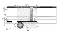
- semiconductor device 700 may be a further embodiment of semiconductor device 400 of FIG. 4 and/or of semiconductor device 600 of FIG. 6 (as illustrated), with the following modifications.
- passivation layer 110 is omitted from semiconductor device 700.
- a compliant dielectric layer is formed in semiconductor device 700 directly adjacent to silicon layer 108.
- second compliant dielectric layer 404 has been formed on silicon layer 108.
- second compliant dielectric layer 404 has also been formed against liner layer 106 in the absence of passivation layer 110.
- compliant dielectric material e.g., compliant dielectric sub-layers 602 including compliant dielectric layer 112, second compliant dielectric layer 404, a third compliant dielectric layer 604 may eliminate the need for passivation layer 110.
- compliant dielectric sub-layers 602 including compliant dielectric layer 112, second compliant dielectric layer 404, a third compliant dielectric layer 604 may eliminate the need for passivation layer 110.
- the effects and benefits of omitting passivation layer 110 are described in further detail below. It should also be noted that the steps of flowchart 300 and flowchart 500 may be performed with respect to semiconductor device 700, according to embodiments.
- one more layers of compliant dielectric material may be applied using molding techniques, chemical vapor deposition (CVD) techniques, spin-on techniques, and/or other similar processes, as would be apparent to persons skilled in the relevant art(s) from the teachings herein.
- CVD chemical vapor deposition
- the semiconductor devices and IC packages described herein may be formed in various ways.
- the following section provides example embodiments for fabricating semiconductor devices and IC packages with compliant dielectric layers.
- FIG. 8 a flowchart providing example steps for assembling an integrated circuit (IC) package with a compliant dielectric layer is shown.
- Semiconductor device 100 of FIG. 1 , semiconductor device 400 of FIG. 2 , semiconductor device 600 of FIG. 6 , semiconductor device 700 of FIG. 7 , and/or any of their respective components/layers may be assembled in accordance with flowchart 800, in embodiments.
- Other structural and operational embodiments will be apparent to persons skilled in the relevant art(s) based on the discussion regarding flowchart 800.
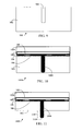
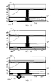
- FIGS. 9-17 respectively show semiconductor device structures 900-1700 at intermediate states of assembly, while FIG. 1 shows a complete semiconductor device 100, as described above.
- Flowchart 800 is described as follows.
- Flowchart 800 begins with step 802.
- an opening is formed in a semiconductor material body having opposing first and second surfaces, the opening formed in the first surface of the semiconductor material body.
- semiconductor device structure 900 is depicted that includes a semiconductor material body 902 with an opening/cavity 904 formed on the first surface thereof. Opening/cavity 904 extends partially through body 902.
- the opening/cavity 904 may be made by etching, drilling, and/or other material removal processes.
- opening/cavity 904 may have a cylindrical shape, although in other embodiments, opening/cavity 904 may have another shape.
- the opening is filled with an electrically conductive material.
- semiconductor device structure 1000 includes opening/cavity 904 filled with an electrically conductive material (e.g., copper, aluminum, tungsten, nickel, another electrically conductive metal, a combination of metals/an alloy, electrically conductive polymer, or other electrically conductive material) to form a partially-formed through silicon via 1006.
- an electrically conductive material e.g., copper, aluminum, tungsten, nickel, another electrically conductive metal, a combination of metals/an alloy, electrically conductive polymer, or other electrically conductive material
- a via liner e.g., liner layer 106 shown in FIG. 10
- liner layer 106 may be formed in opening/cavity 904 and on the first surface of semiconductor material body 902 prior to filling opening/cavity 904 in step 804.
- liner layer 106 may be configured as described above with respect to FIG. 1 .
- Liner layer 106 may be formed of an electrically conductive (e.g., a metal or combination of metals/alloy, etc.) or a non-electrically conductive material (e.g., an oxide, a dielectric material, etc.)
- a first electrically conductive feature is formed on the first surface of the semiconductor material body that is electrically coupled to the electrically conductive material in the filled opening.
- an electrically conductive material such as first metal layer 104 shown in FIG. 10
- first metal layer 104 may be formed on the first surface of semiconductor material body 902.
- a portion of first metal layer 104 e.g., a redistribution layer
- electrical signals may be passed through first metal layer 104 to partially-formed through silicon via 1006.
- first metal layer 104 may be configured as described above with respect to FIG. 1 .
- first dielectric layer e.g., first dielectric layer 102
- semiconductor material body 902 may be formed above semiconductor material body 902
- First dielectric layer 102 may be configured as described above with respect to FIG. 1 .
- a support structure is applied to the first surface of the semiconductor material body.
- a support structure such as support structure 1004 may be applied to the first surface of semiconductor material body 902 using an adhesive layer 1002.
- support structure 1004 and adhesive layer 1002 may be bonded and configured as temporary structures and/or layers which may be subsequently removed.
- Support structure 1004 is configured to provide structural stability during the fabrication/assembly process flow (e.g., of flowchart 800).
- semiconductor device structure 1100 includes a pillar 1102 having a tip surface 1104 that may be formed by etching the second surface (bottom surface in FIG. 11 ) of semiconductor material body 902 and exposing a portion of partially-formed through silicon via 1006. It should be noted that in embodiments, liner layer 106 may still cover the exposed portion of partially-formed through silicon via 1006 that comprises pillar 1102. In some embodiments, various types of etching, e.g., wet etching and dry etching, may be used, and in alternate embodiments, non-etching techniques may be used to expose pillar 1102.
- etching e.g., wet etching and dry etching
- semiconductor material body 902 is substantially formed into silicon layer 108, as described above with respect to FIG. 1 .
- semiconductor device structure 1200 includes silicon layer 108 in place of semiconductor material body 902.
- semiconductor device structure 1200 includes a passivation layer, e.g., passivation layer 110 as described above with respect to FIG. 1 , that may be optionally formed on the etched, exposed surface of semiconductor material body 902 (i.e., at silicon layer 108) after etching.
- Passivation layer 110 may be formed using chemical vapor deposition (CVD) techniques, or similar processes, to deposit an oxide or nitride passivation material on the etched, exposed surface of semiconductor material body 902 (i.e., at silicon layer 108). In embodiments, when present, passivation layer 110 coats and/or surrounds pillar 1102 (over liner layer 106).
- a compliant dielectric material is applied to the etched second surface of the semiconductor material body and surrounding the pillar to form a compliant dielectric material layer, the compliant dielectric material layer having opposing first and second surfaces, the first surface of the compliant dielectric material layer adhering to the second surface of the semiconductor material body.
- semiconductor device structure 1300 includes a compliant dielectric material that is applied to silicon layer 108 (i.e., the etched second surface of semiconductor material body 902) and surrounds pillar 1102 thus forming a compliant dielectric material layer, e.g., compliant dielectric layer 112.
- Compliant dielectric layer 112 has two opposing surfaces, a first surface at silicon layer 108 and a second surface at the bottom of semiconductor device structure 1300, as shown.
- Compliant dielectric layer 112 may be configured and/or selected similarly as described herein, and may be applied using molding techniques, CVD, a spin-on application, and/or other similar processes.
- applying compliant dielectric layer 112 to the etched second surface includes applying compliant dielectric layer 112 to passivation layer 110 such that passivation layer 110 is between silicon layer 108 (i.e., the etched semiconductor material body 902) and compliant dielectric layer 112.
- applying compliant dielectric layer 112 to the etched second surface includes applying multiple sub-layers of compliant dielectric material as described with respect to FIGS. 3-7 herein.
- the bottom surface of semiconductor device structure 1300 may be planarized using a chemical mechanical polishing (CMP) technique or other similar process.
- CMP chemical mechanical polishing
- FIG. 14 shows semiconductor device structure 1400 with a bottom surface 1402 that has undergone a CMP process such that bottom surface 1402 is planar or substantially planar in embodiments.
- Semiconductor device structure 1400 may be a further embodiment of semiconductor device structure 1300 of FIG. 13 .
- the CMP process removes materials and/or layers covering tip surface 1104 of pillar 1102 (e.g., as passivation layer 110) such that the electrically conductive material forming pillar 1102 under tip surface 1104 becomes exposed and configured for electrically conductive connections thereto. Accordingly, through-silicon via 114 is formed.
- a second electrically conductive feature is formed on the second surface of the compliant dielectric material layer in electrical contact with the pillar at the second surface of the compliant dielectric material layer, the pillar being an electrically conductive via through the semiconductor material body and the compliant dielectric material layer.
- FIG. 15 shows semiconductor device structure 1500 with an electrically conductive feature, e.g., a redistribution layer of second metal layer 118, formed on the second surface of compliant dielectric layer 112. Second metal layer 118 is in electrical contact with pillar 1102 (shown in FIG. 13 ) at the second surface of compliant dielectric layer 112.
- an electrically conductive via i.e., through silicon via 114 through silicon layer 108 (i.e., etched semiconductor material body 902) and compliant dielectric layer 112 is completely formed providing electrical connectivity between first metal layer 104 and second metal layer 118.
- FIG. 16 shows semiconductor device structure 1600 that may be a further embodiment of semiconductor device structure 1500 of FIG. 15 .
- Semiconductor device structure 1600 includes second dielectric layer 116 and connector 120, as described above with respect to FIG. 1 , which are formed at the bottom surface of semiconductor device structure 1600, as shown.
- FIG. 17 shows a semiconductor device structure 1700 that may be formed subsequently from semiconductor device structure 1600 of FIG. 16 .
- Semiconductor device structure 1700 includes solder ball/bump 122 (i.e., an interconnect member), as described above with respect to FIG. 1 , which is formed at connector 120 and in electrical contact with an electrically conductive feature such as those in second metal layer 118.
- Solder ball/bump 122 may be formed on connector 120 in any manner, as would be known to persons skilled in the relevant art(s).
- support structure 1004 (and adhesive layer 1002) may be removed from semiconductor device structure 1700, using known techniques (e.g., peeling, delamination through heating or cooling, etc.), to substantially form semiconductor device 100 shown in FIG. 1 .
- steps 802, 804, 806, 808, 810, and/or 812 of flowchart 800 may not be performed. Moreover, steps in addition to or in lieu of steps 802, 804, 806, 808, 810, and/or 812 may be performed (some of which were described above). Further, in some example embodiments, one or more of steps 802, 804, 806, 808, 810, and/or 812 may be performed out of the order shown in FIG. 8 , in an alternate sequence, and/or partially (or completely) concurrently with other steps.
- FIG. 18 shows a flowchart 1800 providing example steps for assembling IC packages with a compliant dielectric layer(s).
- IC packages may be formed that integrate semiconductor device 100 of FIG. 1 , semiconductor device 400 of FIG. 2 , semiconductor device 600 of FIG. 6 , semiconductor device 700 of FIG. 7 , and/or further semiconductor device embodiments described herein.
- Other structural and operational embodiments will be apparent to persons skilled in the relevant art(s) based on the discussion regarding flowchart 1800.
- the exemplary steps of flowchart 1800 are described as follows with respect to the IC packages shown in FIGS. 19 and 20 .
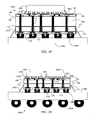
- FIG. 19 illustrates an exemplary IC package 1900.
- IC package 1900 includes semiconductor device 100 of FIG. 1 (configured as an interposer) and an IC die 1902 mounted to the top surface of semiconductor device 100.
- IC package 1900 includes first dielectric layer 102, first metal layer 104, liner layer 106, silicon layer 108, passivation layer 110, compliant dielectric layer 112, a plurality of through silicon vias 114, second dielectric layer 116, second metal layer 118, a plurality of connectors 120, and a plurality of solder balls/bumps 122.
- IC package 1900 is shown mounted to a substrate 1906.
- IC die 1902 includes a plurality of solder balls/bumps 1904 that may be attached and electrically connected to electrically conductive features of semiconductor device 100, such as features in first metal layer 104.
- Substrate 1906 may be a circuit board such as an organic substrate or a printed circuit board (PCB) according to embodiments.
- Solder balls/bumps 122 of semiconductor device 100 may be attached and electrically connected to electrically conductive features 1908 (e.g., land pads) of substrate 1906.
- a first package underfill material 1910 surrounds solder balls/bumps 1904, and a second package underfill material 1912 surrounds solder balls/bumps 122 of semiconductor device 100.
- IC package 2000 includes semiconductor device 100 of FIG. 1 (configured as an interposer), first IC die 1902 and substrate 1906 of FIG. 19 , and a second IC die 2002.
- IC package 2000 includes first dielectric layer 102, first metal layer 104, liner layer 106, silicon layer 108, passivation layer 110, compliant dielectric layer 112, a plurality of through silicon vias 114, second dielectric layer 116, second metal layer 118, a plurality of connectors 120, and a plurality of solder balls/bumps 122.
- First and second IC dies 1902 and 2002 are mounted side-by-side to the top surface of semiconductor device 100 by first and second pluralities of solder balls/bumps 1904 and 2004, respectively.
- Solder balls/bumps 1904 and 2004 are electrically connected to electrically conductive features of semiconductor device 100 (e.g., features in first metal layer 104 shown in FIG. 1 ).
- First package underfill material 1910 surrounds solder balls/bumps 1904
- second package underfill material 1912 surrounds solder balls/bumps 122
- a third package underfill material 2006 surrounds solder balls/bumps 2004.
- Semiconductor device 100 is shown mounted to the top surface of substrate 1906 (similarly to FIG. 19 ) by solder balls/bumps 122.
- IC package 2000 also includes a plurality of substrate solder balls/bumps 2008 attached to a bottom surface of substrate 1906 (in opposition to the top surface of substrate 1906 to which semiconductor device 100 is mounted). Solder balls/bumps 2008 enable IC package 2000 to be mounted to a subsequent circuit board.
- flowchart 1800 provides example steps for assembling IC packages, such as IC packages 1900 and 2000. Flowchart 1800 is described as follows.
- Flowchart 1800 begins with step 1802.
- one or more IC dies are attached to an interposer.
- IC die 1902 is positioned on semiconductor device 100.
- the positioning of IC die 1902 is determined based upon solder balls/bumps 1904 being aligned with electrically conductive features of semiconductor device 100, such as those in first metal layer 104 shown in FIG. 1 .
- IC die 1902 is similarly positioned above semiconductor device 100.
- FIG. 20 illustrates second IC die 2002 is positioned above semiconductor device 100 based upon solder balls/bumps 2004 being aligned with electrically conductive features of semiconductor device 100.
- solder balls/bumps of IC die 1902 are attached to semiconductor device 100. In embodiments, this may be accomplished using a solder reflow process or the like. A similar process may be performed to attach solder balls/bumps 1904 of IC die 1902 and solder balls/bumps 2004 of IC die 2002 to semiconductor device 100 in FIG. 20 .
- package underfill material is applied to the attachment contacts of the IC die(s).
- FIG. 19 shows a first package underfill material 1910 applied to surround solder balls/bumps 1904 of IC die 1902, and a second package underfill material 1912 applied to surround solder balls/bumps of semiconductor device 100 (e.g., solder balls/bump 122).
- first package underfill material 1910 and second package underfill material 1912 may comprise an epoxy and/or other non-electrically conducting materials.
- first package underfill material 1910 is applied to surround solder balls/bumps 1904 of IC die 1902
- second package underfill material 1912 is applied to surround solder balls/bumps semiconductor device 100
- a third package underfill material 2006 is applied to surround solder balls/bumps 2004 of IC die 2002.
- third package underfill material 2006 may comprise an epoxy and/or other non-electrically conducting materials.
- the interposer is attached to the substrate.
- semiconductor device 100 configured as an interposer, is positioned on substrate 1906.
- the positioning of semiconductor device 100 is determined based the positions of solder balls/bumps 122, to be aligned with electrically conductive features 1908 of substrate 1906.
- semiconductor device 100 is similarly positioned above substrate 1906.
- solder balls/bumps of semiconductor device 100 are attached to substrate 1906. In embodiments, this may be accomplished using a solder reflow process or the like. A similar process may be performed to attach the solder balls/bumps of semiconductor device 100 (e.g., instances of solder ball/bump 122) to substrate 1906 of FIG. 20 .
- compliant dielectric layer 112 allows for mechanical and thermal variance with a decrease in stress and damage to components, as described herein.
- one or more steps 1802, 1804, and/or 1806 of flowchart 1800 may not be performed. Moreover, steps in addition to or in lieu of steps 1802, 1804, and/or 1806 may be performed. Further, in some example embodiments, one or more of steps 1802, 1804, and/or 1806 may be performed out of order, in an alternate sequence, and/or partially (or completely) concurrently with other steps.
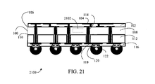
- FIG. 21 illustrates another exemplary IC package 2100, according to an embodiment.
- IC package 2100 includes semiconductor device 100 configured as an integrated circuit die.
- IC package 2100 includes first dielectric layer 102, first metal layer 104, liner layer 106, silicon layer 108, passivation layer 110, compliant dielectric layer 112, a plurality of through silicon vias 114, second dielectric layer 116, second metal layer 118, a plurality of connectors 120, and a plurality of solder balls/bumps 122.
- Solder balls/bumps 122 may be attached and electrically connected to electrically conductive features (e.g., land pads) of a circuit board.
- silicon layer 108 includes an active integrated circuit region 2102 that includes integrated circuitry that provides electrical circuit functionality to IC package 2100 itself.
- IC package 2100 may be considered to be a wafer-level integrated circuit package (e.g., a wafer-level ball grid array package - WLBGA).
- Active integrated circuit region 2102 may be formed on the top surface of silicon layer 108 shown in FIG. 21 , and may be formed by any suitable integrated circuit fabrication process, including by photolithography or other integrated circuit fabrication process. Signals of active integrated circuit region 2102 may be accessible at terminals on a top surface of silicon layer 108 in FIG. 21 .
- routing in metal layer 104 may be used to electrically couple the terminals on the top surface of silicon layer 108 (through vias through first dielectric layer 102) to through silicon vias 114.
- Through silicon vias 114 route signals of the terminals through silicon layer 108 and compliant dielectric layer 112 to be electrically coupled to solder balls/bumps 122 at connectors 120 on the bottom surface of IC package 2100 in FIG. 21 .
- the embodiments described herein provide for improved integrated circuit (IC) packages.
- the embodiments herein provide semiconductor devices and IC packages that include one or more compliant dielectric layers.
- the compliant dielectric layer(s) may be selected so that the coefficient of thermal expansion (CTE) of the compliant dielectric layer(s) matches or approximately matches the CTE of the substrate upon which the IC package is mounted.
- Compliant dielectric material layer(s) may be selected that have a deformability that is greater than a deformability of the semiconductor material body of the IC die or interposer to which they are attached. This allows for flexibility with respect to mechanical stresses that occur during processes and operations that involve heating and cooling of the IC package.
- allowing a portion of an IC package to expand and contract similarly to the substrate on which it rests reduces stress in the device and reduces damage to parts.
- Electrical capacitance may also be reduced through the use of compliant dielectric layers, and improved backside metallization is also achieved on organic, compliant dielectric layers.
- IC packages that include one or more compliant dielectric layers may be created at greater scale than the current state of the art.
- a flip chip interposer such as those described in embodiments herein, allows for a 200%-400% increase in interposer area over the current state of the art (e.g., approx. 600mm 2 ).
- larger IC die may be mounted on substrates that include thick organic, compliant dielectric layers.
- a high density top-pad interconnect can be achieved for flip chip IC die while maintaining CTE matching with a printed circuit board.
- the size of an IC package can be increased to 256mm 2 (16mm x 16mm) with a 0.4mm ball pitch due to the stress buffering provided by the compliant dielectric layers.
- WLBGA pitch may be decreased to approximately 0.3mm.
- compliant dielectric layers can eliminate the need for passivation layers in IC packages as the thick organic, compliant dielectric materials can be sufficient to prevent backside metal diffusion into silicon layers. This results in cost savings for materials and assembly processes, and also reduces capacitance due to the passivation layer properties (high k) which in turn reduces signal propagation delay and power consumption.
- IC packages such as, but not limited to, communication systems, communication devices, computing devices, electronic devices, and/or the like.
- IC packages, their respective components, and/or the techniques described herein may be implemented in hardware, software, firmware, or any combination thereof, and/or may be implemented as hardware logic/electrical circuitry.
- the disclosed technologies can be put into practice using software, firmware, and/or hardware implementations other than those described herein. Any software, firmware, and hardware implementations suitable for performing the functions described herein can be used, such as those described below.
Landscapes
- Physics & Mathematics (AREA)
- Geometry (AREA)
- Internal Circuitry In Semiconductor Integrated Circuit Devices (AREA)
- Production Of Multi-Layered Print Wiring Board (AREA)
Applications Claiming Priority (2)
| Application Number | Priority Date | Filing Date | Title |
|---|---|---|---|
| US201361918373P | 2013-12-19 | 2013-12-19 | |
| US14/147,237 US9431370B2 (en) | 2013-12-19 | 2014-01-03 | Compliant dielectric layer for semiconductor device |
Publications (2)
| Publication Number | Publication Date |
|---|---|
| EP2887393A2 true EP2887393A2 (de) | 2015-06-24 |
| EP2887393A3 EP2887393A3 (de) | 2015-11-25 |
Family
ID=52133765
Family Applications (1)
| Application Number | Title | Priority Date | Filing Date |
|---|---|---|---|
| EP14004185.6A Withdrawn EP2887393A3 (de) | 2013-12-19 | 2014-12-11 | Nachgiebige dielektrische Schicht für ein Halbleiterbauelement |
Country Status (2)
| Country | Link |
|---|---|
| US (1) | US9431370B2 (de) |
| EP (1) | EP2887393A3 (de) |
Cited By (1)
| Publication number | Priority date | Publication date | Assignee | Title |
|---|---|---|---|---|
| CN119623403A (zh) * | 2025-02-14 | 2025-03-14 | 飞骧科技(无锡)有限公司 | 基于位置寻优的封装可靠性优化方法、系统及相关设备 |
Families Citing this family (2)
| Publication number | Priority date | Publication date | Assignee | Title |
|---|---|---|---|---|
| US10763199B2 (en) * | 2018-12-24 | 2020-09-01 | Nanya Technology Corporation | Semiconductor package structure and method for preparing the same |
| US12525541B2 (en) * | 2020-05-22 | 2026-01-13 | Danmarks Tekniske Universitet | Power converter assembly |
Family Cites Families (11)
| Publication number | Priority date | Publication date | Assignee | Title |
|---|---|---|---|---|
| WO1998044564A1 (en) * | 1997-04-02 | 1998-10-08 | Tessera, Inc. | Chip with internal signal routing in external element |
| US6317333B1 (en) * | 1997-08-28 | 2001-11-13 | Mitsubishi Denki Kabushiki Kaisha | Package construction of semiconductor device |
| US6970005B2 (en) * | 2000-08-24 | 2005-11-29 | Texas Instruments Incorporated | Multiple-chip probe and universal tester contact assemblage |
| KR100537892B1 (ko) * | 2003-08-26 | 2005-12-21 | 삼성전자주식회사 | 칩 스택 패키지와 그 제조 방법 |
| US7335972B2 (en) * | 2003-11-13 | 2008-02-26 | Sandia Corporation | Heterogeneously integrated microsystem-on-a-chip |
| EP1739739A4 (de) | 2004-03-26 | 2010-02-24 | Fujikura Ltd | Durchverdrahtungs-board und herstellungsverfahren dafür |
| JP4473935B1 (ja) * | 2009-07-06 | 2010-06-02 | 新光電気工業株式会社 | 多層配線基板 |
| US8519537B2 (en) | 2010-02-26 | 2013-08-27 | Taiwan Semiconductor Manufacturing Company, Ltd. | 3D semiconductor package interposer with die cavity |
| US8298944B1 (en) | 2011-06-01 | 2012-10-30 | Texas Instruments Incorporated | Warpage control for die with protruding TSV tips during thermo-compressive bonding |
| US20130241057A1 (en) | 2012-03-14 | 2013-09-19 | Taiwan Semiconductor Manufacturing Company, Ltd. | Methods and Apparatus for Direct Connections to Through Vias |
| JP5874481B2 (ja) | 2012-03-22 | 2016-03-02 | 富士通株式会社 | 貫通電極の形成方法 |
-
2014
- 2014-01-03 US US14/147,237 patent/US9431370B2/en active Active
- 2014-12-11 EP EP14004185.6A patent/EP2887393A3/de not_active Withdrawn
Non-Patent Citations (1)
| Title |
|---|
| None |
Cited By (1)
| Publication number | Priority date | Publication date | Assignee | Title |
|---|---|---|---|---|
| CN119623403A (zh) * | 2025-02-14 | 2025-03-14 | 飞骧科技(无锡)有限公司 | 基于位置寻优的封装可靠性优化方法、系统及相关设备 |
Also Published As
| Publication number | Publication date |
|---|---|
| US9431370B2 (en) | 2016-08-30 |
| EP2887393A3 (de) | 2015-11-25 |
| US20150179610A1 (en) | 2015-06-25 |
Similar Documents
| Publication | Publication Date | Title |
|---|---|---|
| CN112514062B (zh) | 具有在芯片与封装衬底之间提供电源连接的芯片互连桥的多芯片封装结构 | |
| US10714442B2 (en) | Interconnect structures and methods of forming same | |
| CN110034026B (zh) | 封装件结构和方法 | |
| CN109786266B (zh) | 半导体封装件及其形成方法 | |
| CN109216315B (zh) | 半导体封装及其制造方法 | |
| KR101679935B1 (ko) | 집적 회로 패키지 및 집적 회로 패키지 형성 방법 | |
| CN109937476B (zh) | 晶片级封装和方法 | |
| US9991231B2 (en) | Stacked die integrated circuit | |
| TWI394218B (zh) | 積體電路封裝及其形成方法、晶圓級積體電路封裝結構 | |
| KR101855216B1 (ko) | 칩의 양 측면들로부터의 스테이징된 비아 형성 | |
| CN104851842B (zh) | 包括嵌入式表面安装器件的半导体器件及其形成方法 | |
| US7763965B2 (en) | Stress relief structures for silicon interposers | |
| US20160322317A1 (en) | Semiconductor device and manufacturing method thereof | |
| US9230901B2 (en) | Semiconductor device having chip embedded in heat spreader and electrically connected to interposer and method of manufacturing the same | |
| KR102415484B1 (ko) | 패키지 구조체 및 그 제조 방법 | |
| CN113113381A (zh) | 封装结构及其形成方法 | |
| CN106992160A (zh) | 封装的半导体器件以及封装方法 | |
| CN106298716A (zh) | 封装件结构及其形成方法 | |
| US9548283B2 (en) | Package redistribution layer structure and method of forming same | |
| CN113658873A (zh) | 半导体系统封装及其制造方法 | |
| WO2015054413A1 (en) | Bowl-shaped solder structure | |
| US20130075907A1 (en) | Interconnection Between Integrated Circuit and Package | |
| KR20220102541A (ko) | 반도체 패키지 및 이를 형성하는 방법 | |
| CN112687665A (zh) | 半导体器件及其形成方法 | |
| KR20250029084A (ko) | 반도체 소자 및 방법 |
Legal Events
| Date | Code | Title | Description |
|---|---|---|---|
| PUAI | Public reference made under article 153(3) epc to a published international application that has entered the european phase |
Free format text: ORIGINAL CODE: 0009012 |
|
| 17P | Request for examination filed |
Effective date: 20141211 |
|
| AK | Designated contracting states |
Kind code of ref document: A2 Designated state(s): AL AT BE BG CH CY CZ DE DK EE ES FI FR GB GR HR HU IE IS IT LI LT LU LV MC MK MT NL NO PL PT RO RS SE SI SK SM TR |
|
| AX | Request for extension of the european patent |
Extension state: BA ME |
|
| PUAL | Search report despatched |
Free format text: ORIGINAL CODE: 0009013 |
|
| AK | Designated contracting states |
Kind code of ref document: A3 Designated state(s): AL AT BE BG CH CY CZ DE DK EE ES FI FR GB GR HR HU IE IS IT LI LT LU LV MC MK MT NL NO PL PT RO RS SE SI SK SM TR |
|
| AX | Request for extension of the european patent |
Extension state: BA ME |
|
| RIC1 | Information provided on ipc code assigned before grant |
Ipc: H01L 21/768 20060101ALI20151020BHEP Ipc: H01L 23/498 20060101ALI20151020BHEP Ipc: H01L 23/48 20060101AFI20151020BHEP |
|
| 17Q | First examination report despatched |
Effective date: 20151116 |
|
| RBV | Designated contracting states (corrected) |
Designated state(s): AL AT BE BG CH CY CZ DE DK EE ES FI FR GB GR HR HU IE IS IT LI LT LU LV MC MK MT NL NO PL PT RO RS SE SI SK SM TR |
|
| RAP1 | Party data changed (applicant data changed or rights of an application transferred) |
Owner name: AVAGO TECHNOLOGIES GENERAL IP (SINGAPORE) PTE. LTD |
|
| RAP1 | Party data changed (applicant data changed or rights of an application transferred) |
Owner name: AVAGO TECHNOLOGIES INTERNATIONAL SALES PTE. LIMITE |
|
| STAA | Information on the status of an ep patent application or granted ep patent |
Free format text: STATUS: EXAMINATION IS IN PROGRESS |
|
| RIC1 | Information provided on ipc code assigned before grant |
Ipc: H01L 23/31 20060101ALI20210115BHEP Ipc: H01L 23/498 20060101ALI20210115BHEP Ipc: H01L 23/48 20060101ALI20210115BHEP Ipc: H01L 21/48 20060101AFI20210115BHEP Ipc: H01L 21/768 20060101ALI20210115BHEP |
|
| GRAP | Despatch of communication of intention to grant a patent |
Free format text: ORIGINAL CODE: EPIDOSNIGR1 |
|
| STAA | Information on the status of an ep patent application or granted ep patent |
Free format text: STATUS: GRANT OF PATENT IS INTENDED |
|
| INTG | Intention to grant announced |
Effective date: 20210330 |
|
| STAA | Information on the status of an ep patent application or granted ep patent |
Free format text: STATUS: THE APPLICATION IS DEEMED TO BE WITHDRAWN |
|
| 18D | Application deemed to be withdrawn |
Effective date: 20210810 |