EP2887134A1 - Wärmestrahlungseinheit und Anzeigevorrichtung damit - Google Patents
Wärmestrahlungseinheit und Anzeigevorrichtung damit Download PDFInfo
- Publication number
- EP2887134A1 EP2887134A1 EP14190042.3A EP14190042A EP2887134A1 EP 2887134 A1 EP2887134 A1 EP 2887134A1 EP 14190042 A EP14190042 A EP 14190042A EP 2887134 A1 EP2887134 A1 EP 2887134A1
- Authority
- EP
- European Patent Office
- Prior art keywords
- heat radiation
- display
- displays
- display device
- radiation unit
- Prior art date
- Legal status (The legal status is an assumption and is not a legal conclusion. Google has not performed a legal analysis and makes no representation as to the accuracy of the status listed.)
- Granted
Links
Images


Classifications
-
- G—PHYSICS
- G06—COMPUTING OR CALCULATING; COUNTING
- G06F—ELECTRIC DIGITAL DATA PROCESSING
- G06F3/00—Input arrangements for transferring data to be processed into a form capable of being handled by the computer; Output arrangements for transferring data from processing unit to output unit, e.g. interface arrangements
- G06F3/14—Digital output to display device ; Cooperation and interconnection of the display device with other functional units
- G06F3/1423—Digital output to display device ; Cooperation and interconnection of the display device with other functional units controlling a plurality of local displays, e.g. CRT and flat panel display
- G06F3/1446—Digital output to display device ; Cooperation and interconnection of the display device with other functional units controlling a plurality of local displays, e.g. CRT and flat panel display display composed of modules, e.g. video walls
-
- G—PHYSICS
- G09—EDUCATION; CRYPTOGRAPHY; DISPLAY; ADVERTISING; SEALS
- G09F—DISPLAYING; ADVERTISING; SIGNS; LABELS OR NAME-PLATES; SEALS
- G09F9/00—Indicating arrangements for variable information in which the information is built-up on a support by selection or combination of individual elements
-
- G—PHYSICS
- G02—OPTICS
- G02F—OPTICAL DEVICES OR ARRANGEMENTS FOR THE CONTROL OF LIGHT BY MODIFICATION OF THE OPTICAL PROPERTIES OF THE MEDIA OF THE ELEMENTS INVOLVED THEREIN; NON-LINEAR OPTICS; FREQUENCY-CHANGING OF LIGHT; OPTICAL LOGIC ELEMENTS; OPTICAL ANALOGUE/DIGITAL CONVERTERS
- G02F1/00—Devices or arrangements for the control of the intensity, colour, phase, polarisation or direction of light arriving from an independent light source, e.g. switching, gating or modulating; Non-linear optics
- G02F1/01—Devices or arrangements for the control of the intensity, colour, phase, polarisation or direction of light arriving from an independent light source, e.g. switching, gating or modulating; Non-linear optics for the control of the intensity, phase, polarisation or colour
- G02F1/13—Devices or arrangements for the control of the intensity, colour, phase, polarisation or direction of light arriving from an independent light source, e.g. switching, gating or modulating; Non-linear optics for the control of the intensity, phase, polarisation or colour based on liquid crystals, e.g. single liquid crystal display cells
- G02F1/133—Constructional arrangements; Operation of liquid crystal cells; Circuit arrangements
- G02F1/1333—Constructional arrangements; Manufacturing methods
- G02F1/13336—Combining plural substrates to produce large-area displays, e.g. tiled displays
-
- G—PHYSICS
- G02—OPTICS
- G02F—OPTICAL DEVICES OR ARRANGEMENTS FOR THE CONTROL OF LIGHT BY MODIFICATION OF THE OPTICAL PROPERTIES OF THE MEDIA OF THE ELEMENTS INVOLVED THEREIN; NON-LINEAR OPTICS; FREQUENCY-CHANGING OF LIGHT; OPTICAL LOGIC ELEMENTS; OPTICAL ANALOGUE/DIGITAL CONVERTERS
- G02F1/00—Devices or arrangements for the control of the intensity, colour, phase, polarisation or direction of light arriving from an independent light source, e.g. switching, gating or modulating; Non-linear optics
- G02F1/01—Devices or arrangements for the control of the intensity, colour, phase, polarisation or direction of light arriving from an independent light source, e.g. switching, gating or modulating; Non-linear optics for the control of the intensity, phase, polarisation or colour
- G02F1/13—Devices or arrangements for the control of the intensity, colour, phase, polarisation or direction of light arriving from an independent light source, e.g. switching, gating or modulating; Non-linear optics for the control of the intensity, phase, polarisation or colour based on liquid crystals, e.g. single liquid crystal display cells
- G02F1/133—Constructional arrangements; Operation of liquid crystal cells; Circuit arrangements
- G02F1/1333—Constructional arrangements; Manufacturing methods
- G02F1/133382—Heating or cooling of liquid crystal cells other than for activation, e.g. circuits or arrangements for temperature control, stabilisation or uniform distribution over the cell
- G02F1/133385—Heating or cooling of liquid crystal cells other than for activation, e.g. circuits or arrangements for temperature control, stabilisation or uniform distribution over the cell with cooling means, e.g. fans
-
- H—ELECTRICITY
- H05—ELECTRIC TECHNIQUES NOT OTHERWISE PROVIDED FOR
- H05K—PRINTED CIRCUITS; CASINGS OR CONSTRUCTIONAL DETAILS OF ELECTRIC APPARATUS; MANUFACTURE OF ASSEMBLAGES OF ELECTRICAL COMPONENTS
- H05K7/00—Constructional details common to different types of electric apparatus
- H05K7/20—Modifications to facilitate cooling, ventilating, or heating
- H05K7/20954—Modifications to facilitate cooling, ventilating, or heating for display panels
- H05K7/20963—Heat transfer by conduction from internal heat source to heat radiating structure
Definitions
- Apparatuses consistent with exemplary embodiments relate to a heat radiation unit to decrease temperature of a display device constituting a video wall system and a display device having the heat radiation unit.
- Display devices generally operate to display images on screens thereof.
- a variety of functions, such as a video wall function, may be achieved using the display devices.
- the video wall function refers to a function of perceiving a plurality of display devices as one single screen, by which an input image is enlarged to fit the size corresponding to, for example, 1 ⁇ 4, 2 ⁇ 2, 3 ⁇ 3, 4 ⁇ 4 screens or more.
- the video wall function may be utilized in places such as business meeting rooms, presentations, exhibitions, traffic control or stock trading rooms to provide one large image on the screens of a plurality of display devices, thereby catching the attention of viewers more effectively.
- the video wall system in which neighboring display devices are connected in series, has a problem of an increase in temperature at contact portions between the neighboring display devices.
- a display backlight employing light emitting diodes is classified as an edge type backlight and a direct type backlight according to positions of the LEDs.
- the LEDs are positioned at a side of the display panel.
- the LEDs are positioned under the display panel and have a surface area substantially identical to that of the display panel.
- One or more exemplary embodiments provide a heat radiation unit capable of decreasing temperature of display devices constituting a video wall system and a display device having the heat radiation unit.
- one or more exemplary embodiments provide a heat radiation unit capable of decreasing temperature of a side surface of a display panel and a display device having the heat radiation unit.
- one or more exemplary embodiments provide a heat radiation unit capable of preventing shortening of lifespan of the product by decreasing temperature of the display devices and a display device having the heat radiation unit.
- a display device including: at least two displays arranged adjacent to each other and configured to output an image; and a heat radiation unit interposed between the displays and configured to radiate heat generated by the displays, wherein the heat radiation unit includes: a contact part contacting the displays; and a heat radiation part extending from the contact part and configured to radiate the heat generated by the displays.
- the heat radiation unit may be a heat sink.
- the heat radiation unit may further include an adhesive part that adheres the contact part to the displays.
- the heat radiation part may include a heat radiation plate extending from the contact part and one or more heat radiation protrusions extending from the heat radiation plate.
- the one or more heat radiation protrusions may extend from the contact part in a radial direction.
- the one or more heat radiation protrusions may have different heights.
- the heat radiation unit may be a metal heat radiation plate.
- Each of the displays may include a display module configured to display an image and a case provided at an outer portion of the display module.
- the heat radiation unit may be disposed at a side surface of the case.
- a display device including at least two displays arranged adjacent to each other, wherein each of the displays includes a display module configured to display an image, and a case provided at an outer portion of the display module; and a heat radiation unit interposed between the displays so as to contact a side surface of the case of each of the displays and configured to radiate heat generated by the displays.
- the heat radiation unit may be a heat sink.
- the heat radiation unit may include a contact part contacting the side surface of the case of each of the displays and a heat radiation part extending from the contact part and configured to radiate heat generated by the displays.
- the heat radiation unit may further include an adhesive part that adheres the contact part to the displays.
- the heat radiation part may include a heat radiation plate extending from the contact part and one or more heat radiation protrusions extending from the heat radiation plate.
- the one or more heat radiation protrusions may extend from the contact part in a radial direction by different inclination angles.
- the one or more heat radiation protrusions may have different heights.
- the heat radiation unit may be a metal heat radiation plate.
- Each of the displays may include light emitting diodes (LEDs) provided in at least one of edge portions of the display module, and the heat radiation unit may be disposed at the side surface of the case adjacent to the LEDs.
- LEDs light emitting diodes
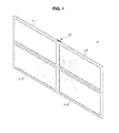
- FIG. 1 is a perspective view schematically illustrating a video wall system including a plurality of display devices according to an exemplary embodiment
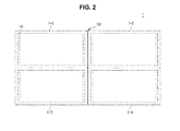
- FIG. 2 is a view schematically illustrating the display device of the video wall system equipped with a heat radiation unit according to a first exemplary embodiment
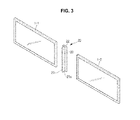
- FIG. 3 is an exploded perspective view schematically illustrating the display device equipped with the heat radiation unit according to the first exemplary embodiment
- FIG. 4 is a sectional view schematically illustrating the display device equipped with the heat radiation unit according to the first exemplary embodiment.
- a display device 1 constituting a video wall system generally includes a plurality of displays, e.g., a first display 1-1, a second display 1-2, a third display 1-3 and a fourth display 1-4.
- the plurality of displays 1-1, 1-2, 1-3 and 1-4 may be arranged in 2 ⁇ 2 matrix, i.e., two rows and two columns.
- the above example is provided for illustrative purposes only and, accordingly, the number and arrangement of the displays of a video wall system may vary.
- the display device 1 of the video wall system may operate such that one of the displays 1-1, 1-2, 1-3 and 1-4 operates as a main display device to control operation of the other sub display devices.
- a separate control device (not shown) may be provided to control operation of the respective displays 1-1, 1-2, 1-3 and 1-4.
- Each of the displays 1-1, 1-2, 1-3 and 1-4 includes a display module 10 to display image information and a case 13 provided at an outer portion of the display module 10 to protect the display module 10 and internal electric components.
- the display module 10 may include a display panel to display an image.
- the display panel may include a thin film transistor (TFT) substrate, a color filter substrate, and a liquid crystal layer disposed between the TFT substrate and the color filter substrate.
- TFT thin film transistor
- Respective pixels emit light independently by driving circuits arranged in a matrix, thereby realizing an image.
- a plurality of LEDs 14 may be provided as a light source and may be arranged at edge portions of the display module 10.
- the LEDs 14 may be arranged apart from each other with a regular interval therebetween in a longitudinal direction. Although it is described and illustrated in this exemplary embodiment that the LEDs 14 are arranged at both left and right edge portions of the display module 10, this and other embodiments are not limited thereto. For example, the LEDs may be arranged only at any one of both edge portions of the display module.
- the case 13 is configured to cover the front edge portions and the rear surface of the display module 10.
- a light guide plate 11 to convert incident light into a surface light source
- a printed circuit board (PCB) 12 to control the display module 10
- a power supply to supply power necessary to drive the display module 10
- a driving module to convert an electric signal from the outside into an image and sound.
- the first display 1-1 and the second display 1-2 may be arranged adjacent to each other (side by side) in a horizontal direction.
- the third display 1-3 and the fourth display 1-4 may be arranged adjacent to each other (side by side) in a horizontal direction.
- the first display 1-1 and the third display 1-3 may be arranged adjacent to each other (stacked) in a vertical direction.
- the second display 1-2 and the fourth display 1-4 may be arranged adjacent to each other (stacked) in a vertical direction.
- Heat radiation units 20 may be interposed between the first display 1-1 and the second display 1-2 and between the third display 1-3 and the fourth display 1-4.
- an internal temperature of the first and second displays 1-1 and 1-2 may rise due to heat generated from the LEDs 14 mounted to the edge portions of the first display 1-1 and the LEDs 14 mounted to the edge portions of the second display 1-2. That is, heat generated by the LEDs 14 of the first display 1-1 may cause the internal temperature of the second display 1-2 to rise and heat generated by the LEDs 14 of the second display 1-2 may cause the internal temperature of the first display 1-1 to rise.
- the heat radiation unit 20 may be interposed between the case 13 of the first display 1-1 and the case 13 of the second display 1-2 to radiate heat generated from the first display 1-1 and the second display 1-2. Similarly, the heat radiation unit 20 may be interposed between the case 13 of the third display 1-3 and the case 13 of the fourth display 1-4 to radiate heat generated from the third display 1-4 and the fourth display 1-4.
- the heat radiation unit 20 is configured to radiate heat generated from the LEDs 14 between the first display 1-1 and the second display 1-2 and between the third display 1-3 and the fourth display 1-4, thereby decreasing temperature of the cases 13 around the LEDs 14.
- the heat radiation unit 20 may include a metal heat radiation plate or a heat sink.
- the heat radiation unit 20 includes a contact part 21 configured to contact the cases 13 of the displays 1-1, 1-2, 1-3 and 1-4 and a heat radiation part 22 extending from the contact part 21 and configured to radiate heat generated from the displays 1-1, 1-2, 1-3 and 1-4.
- the contact part 21 may be configured with a contact surface 21a of the contact part 21 for contact with the case 13.
- the heat radiation unit 20 may further include an adhesive part 30 provided at the contact surface 21a, by which the heat radiation unit 20 is adhered to the cases 13 of the displays 1-1, 1-2, 1-3 and.
- the adhesive part 30 may include an adhesive tape or an adhesive agent.
- the heat radiation part 22 includes a heat radiation plate 23 extending from the contact part 21.
- the heat radiation plate 23 may extend from one end portion of the contact part 21 perpendicularly thereto and may be spaced apart from the rear surface of the case 13 of the first display 1-1 and the rear surface of the case 13 of the second display 1-2.
- FIG. 5 is a view schematically illustrating the display device including a heat radiation unit according to a second exemplary embodiment
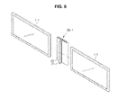
- FIG. 6 is an exploded perspective view schematically illustrating the display device equipped with the heat radiation unit according to the second exemplary embodiment
- FIG. 7 is a view schematically illustrating the display device equipped with a heat radiation unit according to a third exemplary embodiment.
- the heat radiation unit 20 includes a contact part 21 and a heat radiation part 22 extending from the contact part 21.
- the heat radiation part 22 may include a heat radiation plate 23 extending from the contact part 21 and one or more heat radiation protrusions 24 (24a, 24b, ..., 24i and 24j) extending from the heat radiation plate 23.
- the heat radiation protrusions 24 extend outward from the heat radiation plate 23 and are spaced apart from each other, which causes effective convection flow of air between the heat radiation protrusions 24 and, accordingly, a heat radiation area is increased.
- the heat radiation protrusions 24 of the heat radiation unit 20 may respectively have different heights and thicknesses to enhance heat radiation efficiency. Although it is described and illustrated in the exemplary embodiment of FIG. 7 that the height of the heat radiation protrusions 24 gradually decreases from the center portion to the outermost portion and the thickness of the heat radiation protrusions 24 is the same, this and other embodiments are not limited thereto. For example, heat radiation protrusions with different heights may be diversely arranged.
- FIG. 8 is a view schematically illustrating the display device equipped with a heat radiation unit according to a fourth exemplary embodiment
- FIG. 9 is an exploded perspective view schematically illustrating the display device equipped with the heat radiation unit according to the fourth exemplary embodiment.
- heat radiation protrusions 25 of the heat radiation unit 20 extend from one end portion of the contact part 21 in a radial direction by different inclination angles ⁇ .
- the heat radiation protrusions 25 may have a fan shape.
- the heat radiation protrusions 25 have the same height from the contact part 21 and the same thickness, this and other embodiments are not limited thereto.
- the heat radiation protrusion located in the center portion may have the largest height, and the height of the heat radiation protrusions may gradually decrease to the outermost portion while the inclination angle increases.
Landscapes
- Physics & Mathematics (AREA)
- Nonlinear Science (AREA)
- Engineering & Computer Science (AREA)
- General Physics & Mathematics (AREA)
- Crystallography & Structural Chemistry (AREA)
- Mathematical Physics (AREA)
- Chemical & Material Sciences (AREA)
- Optics & Photonics (AREA)
- Theoretical Computer Science (AREA)
- Thermal Sciences (AREA)
- Microelectronics & Electronic Packaging (AREA)
- General Engineering & Computer Science (AREA)
- Human Computer Interaction (AREA)
- Multimedia (AREA)
- Devices For Indicating Variable Information By Combining Individual Elements (AREA)
Applications Claiming Priority (1)
| Application Number | Priority Date | Filing Date | Title |
|---|---|---|---|
| KR1020130157551A KR102136650B1 (ko) | 2013-12-17 | 2013-12-17 | 방열 유닛 및 이를 포함하는 디스플레이 장치 |
Publications (2)
| Publication Number | Publication Date |
|---|---|
| EP2887134A1 true EP2887134A1 (de) | 2015-06-24 |
| EP2887134B1 EP2887134B1 (de) | 2016-09-14 |
Family
ID=51870815
Family Applications (1)
| Application Number | Title | Priority Date | Filing Date |
|---|---|---|---|
| EP14190042.3A Not-in-force EP2887134B1 (de) | 2013-12-17 | 2014-10-23 | Anzeigevorrichtung mit Bildschirmen und einer Wärmestrahlungseinheit zwischen den Bildschirmen. |
Country Status (3)
| Country | Link |
|---|---|
| US (1) | US20150169277A1 (de) |
| EP (1) | EP2887134B1 (de) |
| KR (1) | KR102136650B1 (de) |
Families Citing this family (7)
| Publication number | Priority date | Publication date | Assignee | Title |
|---|---|---|---|---|
| US8974077B2 (en) | 2012-07-30 | 2015-03-10 | Ultravision Technologies, Llc | Heat sink for LED light source |
| US9195281B2 (en) | 2013-12-31 | 2015-11-24 | Ultravision Technologies, Llc | System and method for a modular multi-panel display |
| TWI671721B (zh) * | 2014-09-15 | 2019-09-11 | 比利時商巴而可公司 | 顯示磚、用於顯示磚的框架及其製作方法 |
| CN105516619A (zh) * | 2016-01-26 | 2016-04-20 | 深圳市维冠视界科技股份有限公司 | 一种4k拼接处理器及4k拼接显示系统 |
| WO2020013405A1 (ko) * | 2018-07-13 | 2020-01-16 | (주)엑스퍼넷 | 스마트 식기 및 이의 충전 장치 |
| CN113412025B (zh) * | 2020-03-17 | 2025-05-09 | 群创光电股份有限公司 | 电子装置 |
| KR102452144B1 (ko) * | 2022-06-10 | 2022-10-07 | 주식회사 미디어밸리 | 높낮이 조절구가 구비된 led전광판 |
Citations (3)
| Publication number | Priority date | Publication date | Assignee | Title |
|---|---|---|---|---|
| DE10332012A1 (de) * | 2003-05-23 | 2004-12-30 | Kj Gmbh Installationen | Anzeigetafel |
| WO2012035988A1 (ja) * | 2010-09-14 | 2012-03-22 | シャープ株式会社 | マルチディスプレイ装置 |
| WO2012091530A1 (ko) * | 2010-12-31 | 2012-07-05 | 주식회사 에이브이시스 | 엘씨디 모니터 전광판의 방열 구조와 전광판 관리 시스템 |
Family Cites Families (5)
| Publication number | Priority date | Publication date | Assignee | Title |
|---|---|---|---|---|
| KR200319226Y1 (ko) * | 2003-04-23 | 2003-07-04 | 서머솔루션 주식회사 | 방사형 방열핀을 갖는 히트파이프용 방열판 |
| KR100719675B1 (ko) * | 2005-05-24 | 2007-05-17 | 삼성에스디아이 주식회사 | 플라즈마 디스플레이 장치 |
| KR100703514B1 (ko) * | 2006-04-07 | 2007-04-03 | 삼성에스디아이 주식회사 | 듀얼 화면 모바일 디스플레이 기기 |
| US8599108B2 (en) * | 2007-12-11 | 2013-12-03 | Adti Media, Llc140 | Large scale LED display |
| JP5622498B2 (ja) * | 2010-09-14 | 2014-11-12 | シャープ株式会社 | マルチディスプレイ装置 |
-
2013
- 2013-12-17 KR KR1020130157551A patent/KR102136650B1/ko not_active Expired - Fee Related
-
2014
- 2014-10-23 EP EP14190042.3A patent/EP2887134B1/de not_active Not-in-force
- 2014-11-17 US US14/542,812 patent/US20150169277A1/en not_active Abandoned
Patent Citations (3)
| Publication number | Priority date | Publication date | Assignee | Title |
|---|---|---|---|---|
| DE10332012A1 (de) * | 2003-05-23 | 2004-12-30 | Kj Gmbh Installationen | Anzeigetafel |
| WO2012035988A1 (ja) * | 2010-09-14 | 2012-03-22 | シャープ株式会社 | マルチディスプレイ装置 |
| WO2012091530A1 (ko) * | 2010-12-31 | 2012-07-05 | 주식회사 에이브이시스 | 엘씨디 모니터 전광판의 방열 구조와 전광판 관리 시스템 |
Also Published As
| Publication number | Publication date |
|---|---|
| KR102136650B1 (ko) | 2020-07-23 |
| KR20150071092A (ko) | 2015-06-26 |
| EP2887134B1 (de) | 2016-09-14 |
| US20150169277A1 (en) | 2015-06-18 |
Similar Documents
| Publication | Publication Date | Title |
|---|---|---|
| EP2887134B1 (de) | Anzeigevorrichtung mit Bildschirmen und einer Wärmestrahlungseinheit zwischen den Bildschirmen. | |
| US9217820B2 (en) | Display apparatus | |
| US10185179B2 (en) | Light-emitting apparatus and image display apparatus having fixing members in pixel boundaries | |
| CN106297572A (zh) | 无边框显示装置 | |
| KR20170012659A (ko) | 백라이트 유닛 및 이를 포함하는 액정 표시 장치 | |
| US9176273B2 (en) | Backlight unit for use in multiple-display device | |
| CN104730764A (zh) | 显示装置 | |
| US10228579B2 (en) | Display device and multi display device using the same | |
| CN108022520A (zh) | 显示装置 | |
| WO2016169182A1 (zh) | 显示装置 | |
| CN102692747B (zh) | 电光装置及电子设备 | |
| US9268085B2 (en) | Liquid crystal display device | |
| EP3385782A1 (de) | Lcd-anzeigevorrichtung | |
| US10126480B2 (en) | Display backlight with light mixing structures | |
| WO2012026162A1 (ja) | 照明装置、表示装置、及びテレビ受信装置 | |
| US10935226B2 (en) | Lighting device and display apparatus | |
| KR102134703B1 (ko) | 액정표시장치 | |
| EP2583134A1 (de) | Anzeigevorrichtung | |
| KR102562974B1 (ko) | 입체형 표시장치 | |
| WO2013099718A1 (ja) | 照明装置、バックライト、液晶表示装置及びテレビジョン受信装置 | |
| WO2018128090A1 (ja) | 照明装置及び表示装置 | |
| JP2013157268A (ja) | バックライト装置、表示装置、及びテレビ受信装置 | |
| KR102081120B1 (ko) | 백 라이트 유닛 및 이를 이용한 액정 표시장치 | |
| JP2013165009A (ja) | バックライト装置、表示装置、及びテレビ受信装置 | |
| KR102309511B1 (ko) | 액정표시장치 |
Legal Events
| Date | Code | Title | Description |
|---|---|---|---|
| PUAI | Public reference made under article 153(3) epc to a published international application that has entered the european phase |
Free format text: ORIGINAL CODE: 0009012 |
|
| 17P | Request for examination filed |
Effective date: 20141023 |
|
| AK | Designated contracting states |
Kind code of ref document: A1 Designated state(s): AL AT BE BG CH CY CZ DE DK EE ES FI FR GB GR HR HU IE IS IT LI LT LU LV MC MK MT NL NO PL PT RO RS SE SI SK SM TR |
|
| AX | Request for extension of the european patent |
Extension state: BA ME |
|
| R17P | Request for examination filed (corrected) |
Effective date: 20151118 |
|
| RBV | Designated contracting states (corrected) |
Designated state(s): AL AT BE BG CH CY CZ DE DK EE ES FI FR GB GR HR HU IE IS IT LI LT LU LV MC MK MT NL NO PL PT RO RS SE SI SK SM TR |
|
| GRAP | Despatch of communication of intention to grant a patent |
Free format text: ORIGINAL CODE: EPIDOSNIGR1 |
|
| INTG | Intention to grant announced |
Effective date: 20160425 |
|
| RIN1 | Information on inventor provided before grant (corrected) |
Inventor name: NA, JEONG SHAN Inventor name: KIM, HYUNG KI Inventor name: LEE, HYUNG JIN Inventor name: KIM, SEUNG MIN Inventor name: KO, TAE JUN |
|
| GRAS | Grant fee paid |
Free format text: ORIGINAL CODE: EPIDOSNIGR3 |
|
| GRAA | (expected) grant |
Free format text: ORIGINAL CODE: 0009210 |
|
| AK | Designated contracting states |
Kind code of ref document: B1 Designated state(s): AL AT BE BG CH CY CZ DE DK EE ES FI FR GB GR HR HU IE IS IT LI LT LU LV MC MK MT NL NO PL PT RO RS SE SI SK SM TR |
|
| REG | Reference to a national code |
Ref country code: GB Ref legal event code: FG4D |
|
| REG | Reference to a national code |
Ref country code: CH Ref legal event code: EP |
|
| REG | Reference to a national code |
Ref country code: IE Ref legal event code: FG4D |
|
| REG | Reference to a national code |
Ref country code: AT Ref legal event code: REF Ref document number: 829628 Country of ref document: AT Kind code of ref document: T Effective date: 20161015 |
|
| REG | Reference to a national code |
Ref country code: DE Ref legal event code: R096 Ref document number: 602014003640 Country of ref document: DE |
|
| REG | Reference to a national code |
Ref country code: NL Ref legal event code: FP |
|
| REG | Reference to a national code |
Ref country code: LT Ref legal event code: MG4D |
|
| PG25 | Lapsed in a contracting state [announced via postgrant information from national office to epo] |
Ref country code: HR Free format text: LAPSE BECAUSE OF FAILURE TO SUBMIT A TRANSLATION OF THE DESCRIPTION OR TO PAY THE FEE WITHIN THE PRESCRIBED TIME-LIMIT Effective date: 20160914 Ref country code: NO Free format text: LAPSE BECAUSE OF FAILURE TO SUBMIT A TRANSLATION OF THE DESCRIPTION OR TO PAY THE FEE WITHIN THE PRESCRIBED TIME-LIMIT Effective date: 20161214 Ref country code: RS Free format text: LAPSE BECAUSE OF FAILURE TO SUBMIT A TRANSLATION OF THE DESCRIPTION OR TO PAY THE FEE WITHIN THE PRESCRIBED TIME-LIMIT Effective date: 20160914 Ref country code: LT Free format text: LAPSE BECAUSE OF FAILURE TO SUBMIT A TRANSLATION OF THE DESCRIPTION OR TO PAY THE FEE WITHIN THE PRESCRIBED TIME-LIMIT Effective date: 20160914 Ref country code: FI Free format text: LAPSE BECAUSE OF FAILURE TO SUBMIT A TRANSLATION OF THE DESCRIPTION OR TO PAY THE FEE WITHIN THE PRESCRIBED TIME-LIMIT Effective date: 20160914 |
|
| REG | Reference to a national code |
Ref country code: AT Ref legal event code: MK05 Ref document number: 829628 Country of ref document: AT Kind code of ref document: T Effective date: 20160914 |
|
| PG25 | Lapsed in a contracting state [announced via postgrant information from national office to epo] |
Ref country code: SE Free format text: LAPSE BECAUSE OF FAILURE TO SUBMIT A TRANSLATION OF THE DESCRIPTION OR TO PAY THE FEE WITHIN THE PRESCRIBED TIME-LIMIT Effective date: 20160914 Ref country code: GR Free format text: LAPSE BECAUSE OF FAILURE TO SUBMIT A TRANSLATION OF THE DESCRIPTION OR TO PAY THE FEE WITHIN THE PRESCRIBED TIME-LIMIT Effective date: 20161215 Ref country code: BE Free format text: LAPSE BECAUSE OF NON-PAYMENT OF DUE FEES Effective date: 20161031 Ref country code: LV Free format text: LAPSE BECAUSE OF FAILURE TO SUBMIT A TRANSLATION OF THE DESCRIPTION OR TO PAY THE FEE WITHIN THE PRESCRIBED TIME-LIMIT Effective date: 20160914 |
|
| PG25 | Lapsed in a contracting state [announced via postgrant information from national office to epo] |
Ref country code: RO Free format text: LAPSE BECAUSE OF FAILURE TO SUBMIT A TRANSLATION OF THE DESCRIPTION OR TO PAY THE FEE WITHIN THE PRESCRIBED TIME-LIMIT Effective date: 20160914 Ref country code: EE Free format text: LAPSE BECAUSE OF FAILURE TO SUBMIT A TRANSLATION OF THE DESCRIPTION OR TO PAY THE FEE WITHIN THE PRESCRIBED TIME-LIMIT Effective date: 20160914 |
|
| PG25 | Lapsed in a contracting state [announced via postgrant information from national office to epo] |
Ref country code: IS Free format text: LAPSE BECAUSE OF FAILURE TO SUBMIT A TRANSLATION OF THE DESCRIPTION OR TO PAY THE FEE WITHIN THE PRESCRIBED TIME-LIMIT Effective date: 20170114 Ref country code: PL Free format text: LAPSE BECAUSE OF FAILURE TO SUBMIT A TRANSLATION OF THE DESCRIPTION OR TO PAY THE FEE WITHIN THE PRESCRIBED TIME-LIMIT Effective date: 20160914 Ref country code: AT Free format text: LAPSE BECAUSE OF FAILURE TO SUBMIT A TRANSLATION OF THE DESCRIPTION OR TO PAY THE FEE WITHIN THE PRESCRIBED TIME-LIMIT Effective date: 20160914 Ref country code: ES Free format text: LAPSE BECAUSE OF FAILURE TO SUBMIT A TRANSLATION OF THE DESCRIPTION OR TO PAY THE FEE WITHIN THE PRESCRIBED TIME-LIMIT Effective date: 20160914 Ref country code: BG Free format text: LAPSE BECAUSE OF FAILURE TO SUBMIT A TRANSLATION OF THE DESCRIPTION OR TO PAY THE FEE WITHIN THE PRESCRIBED TIME-LIMIT Effective date: 20161214 Ref country code: SK Free format text: LAPSE BECAUSE OF FAILURE TO SUBMIT A TRANSLATION OF THE DESCRIPTION OR TO PAY THE FEE WITHIN THE PRESCRIBED TIME-LIMIT Effective date: 20160914 Ref country code: SM Free format text: LAPSE BECAUSE OF FAILURE TO SUBMIT A TRANSLATION OF THE DESCRIPTION OR TO PAY THE FEE WITHIN THE PRESCRIBED TIME-LIMIT Effective date: 20160914 Ref country code: BE Free format text: LAPSE BECAUSE OF FAILURE TO SUBMIT A TRANSLATION OF THE DESCRIPTION OR TO PAY THE FEE WITHIN THE PRESCRIBED TIME-LIMIT Effective date: 20160914 Ref country code: CZ Free format text: LAPSE BECAUSE OF FAILURE TO SUBMIT A TRANSLATION OF THE DESCRIPTION OR TO PAY THE FEE WITHIN THE PRESCRIBED TIME-LIMIT Effective date: 20160914 Ref country code: PT Free format text: LAPSE BECAUSE OF FAILURE TO SUBMIT A TRANSLATION OF THE DESCRIPTION OR TO PAY THE FEE WITHIN THE PRESCRIBED TIME-LIMIT Effective date: 20170116 |
|
| REG | Reference to a national code |
Ref country code: DE Ref legal event code: R097 Ref document number: 602014003640 Country of ref document: DE |
|
| PG25 | Lapsed in a contracting state [announced via postgrant information from national office to epo] |
Ref country code: IT Free format text: LAPSE BECAUSE OF FAILURE TO SUBMIT A TRANSLATION OF THE DESCRIPTION OR TO PAY THE FEE WITHIN THE PRESCRIBED TIME-LIMIT Effective date: 20160914 |
|
| PLBE | No opposition filed within time limit |
Free format text: ORIGINAL CODE: 0009261 |
|
| STAA | Information on the status of an ep patent application or granted ep patent |
Free format text: STATUS: NO OPPOSITION FILED WITHIN TIME LIMIT |
|
| REG | Reference to a national code |
Ref country code: IE Ref legal event code: MM4A |
|
| REG | Reference to a national code |
Ref country code: FR Ref legal event code: ST Effective date: 20170630 |
|
| PG25 | Lapsed in a contracting state [announced via postgrant information from national office to epo] |
Ref country code: DK Free format text: LAPSE BECAUSE OF FAILURE TO SUBMIT A TRANSLATION OF THE DESCRIPTION OR TO PAY THE FEE WITHIN THE PRESCRIBED TIME-LIMIT Effective date: 20160914 Ref country code: FR Free format text: LAPSE BECAUSE OF NON-PAYMENT OF DUE FEES Effective date: 20161114 |
|
| 26N | No opposition filed |
Effective date: 20170615 |
|
| PG25 | Lapsed in a contracting state [announced via postgrant information from national office to epo] |
Ref country code: LU Free format text: LAPSE BECAUSE OF NON-PAYMENT OF DUE FEES Effective date: 20161023 |
|
| PG25 | Lapsed in a contracting state [announced via postgrant information from national office to epo] |
Ref country code: SI Free format text: LAPSE BECAUSE OF FAILURE TO SUBMIT A TRANSLATION OF THE DESCRIPTION OR TO PAY THE FEE WITHIN THE PRESCRIBED TIME-LIMIT Effective date: 20160914 Ref country code: IE Free format text: LAPSE BECAUSE OF NON-PAYMENT OF DUE FEES Effective date: 20161023 |
|
| PG25 | Lapsed in a contracting state [announced via postgrant information from national office to epo] |
Ref country code: HU Free format text: LAPSE BECAUSE OF FAILURE TO SUBMIT A TRANSLATION OF THE DESCRIPTION OR TO PAY THE FEE WITHIN THE PRESCRIBED TIME-LIMIT; INVALID AB INITIO Effective date: 20141023 |
|
| REG | Reference to a national code |
Ref country code: CH Ref legal event code: PL |
|
| PG25 | Lapsed in a contracting state [announced via postgrant information from national office to epo] |
Ref country code: MC Free format text: LAPSE BECAUSE OF FAILURE TO SUBMIT A TRANSLATION OF THE DESCRIPTION OR TO PAY THE FEE WITHIN THE PRESCRIBED TIME-LIMIT Effective date: 20160914 Ref country code: MK Free format text: LAPSE BECAUSE OF FAILURE TO SUBMIT A TRANSLATION OF THE DESCRIPTION OR TO PAY THE FEE WITHIN THE PRESCRIBED TIME-LIMIT Effective date: 20160914 Ref country code: CY Free format text: LAPSE BECAUSE OF FAILURE TO SUBMIT A TRANSLATION OF THE DESCRIPTION OR TO PAY THE FEE WITHIN THE PRESCRIBED TIME-LIMIT Effective date: 20160914 Ref country code: MT Free format text: LAPSE BECAUSE OF NON-PAYMENT OF DUE FEES Effective date: 20161031 |
|
| PG25 | Lapsed in a contracting state [announced via postgrant information from national office to epo] |
Ref country code: LI Free format text: LAPSE BECAUSE OF NON-PAYMENT OF DUE FEES Effective date: 20171031 Ref country code: CH Free format text: LAPSE BECAUSE OF NON-PAYMENT OF DUE FEES Effective date: 20171031 |
|
| PG25 | Lapsed in a contracting state [announced via postgrant information from national office to epo] |
Ref country code: TR Free format text: LAPSE BECAUSE OF FAILURE TO SUBMIT A TRANSLATION OF THE DESCRIPTION OR TO PAY THE FEE WITHIN THE PRESCRIBED TIME-LIMIT Effective date: 20160914 Ref country code: AL Free format text: LAPSE BECAUSE OF FAILURE TO SUBMIT A TRANSLATION OF THE DESCRIPTION OR TO PAY THE FEE WITHIN THE PRESCRIBED TIME-LIMIT Effective date: 20160914 |
|
| GBPC | Gb: european patent ceased through non-payment of renewal fee |
Effective date: 20181023 |
|
| PG25 | Lapsed in a contracting state [announced via postgrant information from national office to epo] |
Ref country code: GB Free format text: LAPSE BECAUSE OF NON-PAYMENT OF DUE FEES Effective date: 20181023 |
|
| PGFP | Annual fee paid to national office [announced via postgrant information from national office to epo] |
Ref country code: NL Payment date: 20220921 Year of fee payment: 9 |
|
| PGFP | Annual fee paid to national office [announced via postgrant information from national office to epo] |
Ref country code: DE Payment date: 20220621 Year of fee payment: 9 |
|
| REG | Reference to a national code |
Ref country code: DE Ref legal event code: R119 Ref document number: 602014003640 Country of ref document: DE |
|
| REG | Reference to a national code |
Ref country code: NL Ref legal event code: MM Effective date: 20231101 |
|
| PG25 | Lapsed in a contracting state [announced via postgrant information from national office to epo] |
Ref country code: NL Free format text: LAPSE BECAUSE OF NON-PAYMENT OF DUE FEES Effective date: 20231101 |
|
| PG25 | Lapsed in a contracting state [announced via postgrant information from national office to epo] |
Ref country code: NL Free format text: LAPSE BECAUSE OF NON-PAYMENT OF DUE FEES Effective date: 20231101 Ref country code: DE Free format text: LAPSE BECAUSE OF NON-PAYMENT OF DUE FEES Effective date: 20240501 |