EP2882267A2 - Wiring substrate, light emitting device, and manufacturing method of wiring substrate - Google Patents
Wiring substrate, light emitting device, and manufacturing method of wiring substrate Download PDFInfo
- Publication number
- EP2882267A2 EP2882267A2 EP15153328.8A EP15153328A EP2882267A2 EP 2882267 A2 EP2882267 A2 EP 2882267A2 EP 15153328 A EP15153328 A EP 15153328A EP 2882267 A2 EP2882267 A2 EP 2882267A2
- Authority
- EP
- European Patent Office
- Prior art keywords
- layer
- light emitting
- reflective layer
- wiring
- substrate
- Prior art date
- Legal status (The legal status is an assumption and is not a legal conclusion. Google has not performed a legal analysis and makes no representation as to the accuracy of the status listed.)
- Withdrawn
Links
Images





Classifications
-
- H—ELECTRICITY
- H10—SEMICONDUCTOR DEVICES; ELECTRIC SOLID-STATE DEVICES NOT OTHERWISE PROVIDED FOR
- H10H—INORGANIC LIGHT-EMITTING SEMICONDUCTOR DEVICES HAVING POTENTIAL BARRIERS
- H10H20/00—Individual inorganic light-emitting semiconductor devices having potential barriers, e.g. light-emitting diodes [LED]
- H10H20/80—Constructional details
- H10H20/85—Packages
- H10H20/855—Optical field-shaping means, e.g. lenses
- H10H20/856—Reflecting means
-
- H—ELECTRICITY
- H05—ELECTRIC TECHNIQUES NOT OTHERWISE PROVIDED FOR
- H05K—PRINTED CIRCUITS; CASINGS OR CONSTRUCTIONAL DETAILS OF ELECTRIC APPARATUS; MANUFACTURE OF ASSEMBLAGES OF ELECTRICAL COMPONENTS
- H05K3/00—Apparatus or processes for manufacturing printed circuits
- H05K3/0058—Laminating printed circuit boards onto other substrates, e.g. metallic substrates
- H05K3/0061—Laminating printed circuit boards onto other substrates, e.g. metallic substrates onto a metallic substrate, e.g. a heat sink
-
- H—ELECTRICITY
- H05—ELECTRIC TECHNIQUES NOT OTHERWISE PROVIDED FOR
- H05K—PRINTED CIRCUITS; CASINGS OR CONSTRUCTIONAL DETAILS OF ELECTRIC APPARATUS; MANUFACTURE OF ASSEMBLAGES OF ELECTRICAL COMPONENTS
- H05K3/00—Apparatus or processes for manufacturing printed circuits
- H05K3/10—Apparatus or processes for manufacturing printed circuits in which conductive material is applied to the insulating support in such a manner as to form the desired conductive pattern
-
- H—ELECTRICITY
- H05—ELECTRIC TECHNIQUES NOT OTHERWISE PROVIDED FOR
- H05K—PRINTED CIRCUITS; CASINGS OR CONSTRUCTIONAL DETAILS OF ELECTRIC APPARATUS; MANUFACTURE OF ASSEMBLAGES OF ELECTRICAL COMPONENTS
- H05K3/00—Apparatus or processes for manufacturing printed circuits
- H05K3/10—Apparatus or processes for manufacturing printed circuits in which conductive material is applied to the insulating support in such a manner as to form the desired conductive pattern
- H05K3/20—Apparatus or processes for manufacturing printed circuits in which conductive material is applied to the insulating support in such a manner as to form the desired conductive pattern by affixing prefabricated conductor pattern
- H05K3/205—Apparatus or processes for manufacturing printed circuits in which conductive material is applied to the insulating support in such a manner as to form the desired conductive pattern by affixing prefabricated conductor pattern using a pattern electroplated or electroformed on a metallic carrier
-
- H—ELECTRICITY
- H05—ELECTRIC TECHNIQUES NOT OTHERWISE PROVIDED FOR
- H05K—PRINTED CIRCUITS; CASINGS OR CONSTRUCTIONAL DETAILS OF ELECTRIC APPARATUS; MANUFACTURE OF ASSEMBLAGES OF ELECTRICAL COMPONENTS
- H05K1/00—Printed circuits
- H05K1/02—Details
- H05K1/0274—Optical details, e.g. printed circuits comprising integral optical means
-
- H—ELECTRICITY
- H05—ELECTRIC TECHNIQUES NOT OTHERWISE PROVIDED FOR
- H05K—PRINTED CIRCUITS; CASINGS OR CONSTRUCTIONAL DETAILS OF ELECTRIC APPARATUS; MANUFACTURE OF ASSEMBLAGES OF ELECTRICAL COMPONENTS
- H05K2201/00—Indexing scheme relating to printed circuits covered by H05K1/00
- H05K2201/01—Dielectrics
- H05K2201/0183—Dielectric layers
- H05K2201/0195—Dielectric or adhesive layers comprising a plurality of layers, e.g. in a multilayer structure
-
- H—ELECTRICITY
- H05—ELECTRIC TECHNIQUES NOT OTHERWISE PROVIDED FOR
- H05K—PRINTED CIRCUITS; CASINGS OR CONSTRUCTIONAL DETAILS OF ELECTRIC APPARATUS; MANUFACTURE OF ASSEMBLAGES OF ELECTRICAL COMPONENTS
- H05K2201/00—Indexing scheme relating to printed circuits covered by H05K1/00
- H05K2201/03—Conductive materials
- H05K2201/0332—Structure of the conductor
- H05K2201/0364—Conductor shape
- H05K2201/0376—Flush conductors, i.e. flush with the surface of the printed circuit
-
- H—ELECTRICITY
- H05—ELECTRIC TECHNIQUES NOT OTHERWISE PROVIDED FOR
- H05K—PRINTED CIRCUITS; CASINGS OR CONSTRUCTIONAL DETAILS OF ELECTRIC APPARATUS; MANUFACTURE OF ASSEMBLAGES OF ELECTRICAL COMPONENTS
- H05K2201/00—Indexing scheme relating to printed circuits covered by H05K1/00
- H05K2201/09—Shape and layout
- H05K2201/09209—Shape and layout details of conductors
- H05K2201/09372—Pads and lands
- H05K2201/09409—Multiple rows of pads, lands, terminals or dummy patterns; Multiple rows of mounted components
-
- H—ELECTRICITY
- H05—ELECTRIC TECHNIQUES NOT OTHERWISE PROVIDED FOR
- H05K—PRINTED CIRCUITS; CASINGS OR CONSTRUCTIONAL DETAILS OF ELECTRIC APPARATUS; MANUFACTURE OF ASSEMBLAGES OF ELECTRICAL COMPONENTS
- H05K2201/00—Indexing scheme relating to printed circuits covered by H05K1/00
- H05K2201/10—Details of components or other objects attached to or integrated in a printed circuit board
- H05K2201/10007—Types of components
- H05K2201/10106—Light emitting diode [LED]
-
- H—ELECTRICITY
- H05—ELECTRIC TECHNIQUES NOT OTHERWISE PROVIDED FOR
- H05K—PRINTED CIRCUITS; CASINGS OR CONSTRUCTIONAL DETAILS OF ELECTRIC APPARATUS; MANUFACTURE OF ASSEMBLAGES OF ELECTRICAL COMPONENTS
- H05K2201/00—Indexing scheme relating to printed circuits covered by H05K1/00
- H05K2201/20—Details of printed circuits not provided for in H05K2201/01 - H05K2201/10
- H05K2201/2054—Light-reflecting surface, e.g. conductors, substrates, coatings, dielectrics
-
- H—ELECTRICITY
- H05—ELECTRIC TECHNIQUES NOT OTHERWISE PROVIDED FOR
- H05K—PRINTED CIRCUITS; CASINGS OR CONSTRUCTIONAL DETAILS OF ELECTRIC APPARATUS; MANUFACTURE OF ASSEMBLAGES OF ELECTRICAL COMPONENTS
- H05K3/00—Apparatus or processes for manufacturing printed circuits
- H05K3/0011—Working of insulating substrates or insulating layers
- H05K3/0014—Shaping of the substrate, e.g. by moulding
-
- H—ELECTRICITY
- H10—SEMICONDUCTOR DEVICES; ELECTRIC SOLID-STATE DEVICES NOT OTHERWISE PROVIDED FOR
- H10W—GENERIC PACKAGES, INTERCONNECTIONS, CONNECTORS OR OTHER CONSTRUCTIONAL DETAILS OF DEVICES COVERED BY CLASS H10
- H10W72/00—Interconnections or connectors in packages
- H10W72/20—Bump connectors, e.g. solder bumps or copper pillars; Dummy bumps; Thermal bumps
-
- H—ELECTRICITY
- H10—SEMICONDUCTOR DEVICES; ELECTRIC SOLID-STATE DEVICES NOT OTHERWISE PROVIDED FOR
- H10W—GENERIC PACKAGES, INTERCONNECTIONS, CONNECTORS OR OTHER CONSTRUCTIONAL DETAILS OF DEVICES COVERED BY CLASS H10
- H10W90/00—Package configurations
-
- Y—GENERAL TAGGING OF NEW TECHNOLOGICAL DEVELOPMENTS; GENERAL TAGGING OF CROSS-SECTIONAL TECHNOLOGIES SPANNING OVER SEVERAL SECTIONS OF THE IPC; TECHNICAL SUBJECTS COVERED BY FORMER USPC CROSS-REFERENCE ART COLLECTIONS [XRACs] AND DIGESTS
- Y10—TECHNICAL SUBJECTS COVERED BY FORMER USPC
- Y10T—TECHNICAL SUBJECTS COVERED BY FORMER US CLASSIFICATION
- Y10T29/00—Metal working
- Y10T29/49—Method of mechanical manufacture
- Y10T29/49002—Electrical device making
- Y10T29/49117—Conductor or circuit manufacturing
- Y10T29/49124—On flat or curved insulated base, e.g., printed circuit, etc.
- Y10T29/49155—Manufacturing circuit on or in base
Definitions
- the present disclosure relates to a wiring substrate, a light emitting device, and a manufacturing method of the wiring substrate.
- the usage of the light emitting device has been expanded to an illumination apparatus, a display apparatus, and the like.
- a plurality of light emitting elements are preferably mounted with high density.
- miniaturization of the light emitting element has been developed.
- miniaturization of bumps used to mount the light emitting element in a flip-chip form on the wiring layers has been developed, and thus a gap between the light emitting element and the wiring layers becomes narrowed.
- a reflective layer having high reflectance is formed on an element mounting surface.
- the reflective layer is formed, there is a problem in that the reflective layer and the fine light emitting element tend to interfere (contact) with each other. For this reason, it is desirable to develop a light emitting device which can suppress interference between the reflective layer and the light emitting element and mount the fine light emitting element stably thereon.
- Exemplary embodiments of the present invention address the above disadvantages and other disadvantages not described above.
- the present invention is not required to overcome the disadvantages described above, and thus, an exemplary embodiment of the present invention may not overcome any disadvantages described above.
- a wiring substrate includes: a heat sink; an insulating member on the heat sink; a wiring pattern embedded in the insulating member and including a first surface and a second surface opposite to the first surface, the second surface contacting the insulating member; and a metal layer on the first surface of the wiring pattern, wherein a surface of the metal layer is flush with an exposed surface of the insulating member.
- the aspect of the present invention it is possible to provide a wiring substrate capable of suppressing interference between the reflective layer and the light emitting element and accommodating the miniaturization of the light emitting element.
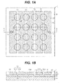
- a wiring substrate 1 includes a heat sink 10, an insulating layer 20 covering the upper surface of the heat sink 10, a reflective layer 30 formed on the insulating layer 20, wiring patterns 40 embedded in the reflective layer 30, and metal layers 50 formed on the wiring patterns 40.
- This wiring substrate 1 is a wiring substrate applied to, for example, a light emitting device.
- the heat sink 10 is, for example, an approximately rectangular thin plate in plan view.
- a metal with favorable heat conductivity such as copper (Cu) or aluminum (Al), or an alloy including at least one of these metals may be used.
- a ceramic material with favorable heat conductivity such as aluminum nitride or alumina may be used.
- the thickness of the heat sink 10 may be, for example, about 0.5 mm to 1.0 mm.
- the insulating layer 20 is formed so as to cover the entire upper surface of the heat sink 10.
- an insulating resin with high heat conductivity for example, about 1 W/mK to 10 W/mK
- an insulating resin such as a polyimide resin or an epoxy resin, or a resin material where a filler such as silica or alumina is mixed with the resin may be used.
- the thickness of the insulating layer 20 may be, for example, about 50 ⁇ m to 80 ⁇ m.
- the insulating layer 20 has a function of insulating the heat sink 10 from the wiring patterns 40, and a function of adhering the heat sink 10 to the reflective layer 30. Further, in a case where the insulating layer 20 has high insulation properties, the insulating layer 20 is preferably formed thinly from the viewpoint of heat dissipation.
- the reflective layer 30 is formed so as to cover the entire first main surface 20A of the insulating layer 20.
- the reflective layer 30 has high reflectance. Specifically, the reflective layer 30 has reflectance of 50% or more (preferably, 80% or more) between the wavelength 450 nm to 700 nm.
- the reflective layer 30 is also referred to as a white resist layer.
- a white insulating resin may be used as a material of the reflective layer 30, for example.
- a white insulating resin for example, a resin material where a filler or a pigment formed from white titanium oxide (TiO 2 ) or barium sulfate (BaSO 4 ) is contained in an epoxy resin, a silicon resin, or an organopolysiloxane resin.
- the reflective layer 30 (white resist layers) covers the outermost surface of the wiring substrate 1, and thereby it is possible to reduce light amount loss of light emitting elements by increasing the reflectance of light from the light emitting elements mounted on the wiring substrate 1 as well as protecting the wiring patterns 40.
- the thickness of the reflective layer 30 may be, for example, 20 ⁇ m to 130 ⁇ m.
- recessed portions 31 are formed at necessary locations ( Fig. 1B , five).
- Each of the recessed portions 31 is formed from the first main surface 30A of the reflective layer 30 to a middle position of the reflective layer 30 in the thickness direction. That is, each of the recessed portions 31 is formed such that the bottom surface 31A of the recessed portion 31 is positioned in the middle of the reflective layer 30 in the thickness direction.
- a planar shape of the recessed portion 31 is formed in a strip shape in plan view or in a rectangular shape in plan view.
- the plurality of recessed portions 31 are formed in parallel so as to be adjacent to each other.
- the wiring patterns 40 are formed on the bottom surfaces 31A of the respective recessed portions 31.
- the plurality of wiring patterns 40 are formed in parallel so as to be adjacent to each other.
- the side surface of each wiring pattern 40 is covered by the reflective layer 30 forming the side walls of the recessed portions 31.
- the adjacent wiring patterns 40 are electrically separated by the reflective layer 30 forming the side walls of the recessed portions 31.
- the wiring pattern 40 is formed so as to be embedded in the reflective layer 30.
- a planar shape of each wiring pattern 40 is formed in a strip shape in plan view or in a rectangular shape in plan view in the same manner as the planar shape of the recessed portion 31.
- the wiring pattern 40 for example, copper or a copper alloy may be used as a material of the wiring pattern 40.
- the thickness of the wiring pattern 40 may be, for example, about 30 ⁇ m to 100 ⁇ m.
- the distance between the adjacent wiring patterns 40 may be, for example, about 0.1 mm to 0.3 mm.
- the wiring pattern 40 is embedded in the reflective layer in such a manner that at least a substantial portion of its side surface (e.g. more than 50% or even more than 80% of or all of its side surface) is in contact with the reflective layer 30, and that possibly also its bottom surface is in contact with the reflective layer 30.
- the metal layer 50 is formed in the recessed portion 31 so as to cover the entire first main surface 40A (the upper surface in Fig. 1B ) of each wiring pattern 40.
- a plurality of (in Fig. 1A , five) metal layers 50 with a strip shape in plan view (a rectangular shape in plan view) are formed in parallel so as to be adjacent to each other.
- the adjacent metal layers 50 are electrically separated by the reflective layer 30 forming the side walls of the recessed portions 31.
- each of the metal layers 50 is formed such that the first main surface 50A (the upper surface in Fig. 1B ) thereof is flush with the first main surface 30A of the reflective layer 30.
- the metal layers 50 exposed from the reflective layer 30 have a plurality of regions which are mounting regions CA in which light emitting elements 60 (refer to Fig. 2 ) are mounted, and have a pair of terminal regions TA functioning as electrode terminals.
- the mounting regions CA are arranged in a matrix (4x4 in Fig. 1A ) on the metal layers 50.
- a pair of metal layers 50 which are separated by the reflective layer 30 forming the side walls of the recessed portions 31 and are formed with the reflective layer 30 interposed therebetween are exposed to outside.
- the pair of metal layers 50 respectively function as pads 50P to which the light emitting elements 60 (refer to Fig. 2 ) are bonded.
- a pair of terminal regions TA are disposed on the metal layers 50 to the outside of the mounting regions CA.
- a pair of terminal regions TA are formed on two metal layers 50 disposed at the outermost positions of the five metal layers 50 and are formed to the outside of the mounting regions CA disposed in the metal layers 50.
- An example of the metal layer 50 may include a silver (Ag) layer, a nickel (Ni)/gold (Au) layer (a metal layer where an Ni layer and an Au layer are formed in this order), an Ni/Ag layer (a metal layer where an Ni layer and an Ag layer are formed in this order), an Ni/palladium (Pd)/Au layer (a metal layer where an Ni layer, a Pd layer, and an Au layer are formed in this order), or the like.
- an example of the metal layer 50 may include an Ni/Pd/Ag layer (a metal layer where an Ni layer, a Pd layer, and an Ag layer are formed in this order), an Ni/Pd/Ag/Au layer (an Ni layer, a Pd layer, an Ag layer, and an Au layer are formed in this order), or the like.
- the thickness of the Ni layer may be about 1 ⁇ m to 10 ⁇ m
- the thickness of the Au layer may be about 0.05 ⁇ m to 2 ⁇ m.
- the light emitting device 2 includes the above-described wiring substrate 1, a plurality of (in Fig. 2A , sixteen) light emitting elements 60 mounted on the wiring substrate 1, and an encapsulating resin 65 which encapsulates the light emitting elements 60 and the like.
- Each light emitting element 60 is mounted on a pair of pads 50P formed in each mounting region CA of the wiring substrate 1. Specifically, each light emitting element 60 is flip-chip mounted on two pads 50P formed on both sides of the reflective layer 30 so as to cross over the reflective layer 30 formed between the pair of pads 50P, that is, the reflective layer 30 forming the side walls of the recessed portions 31. More specifically, one bump 61 formed on one surface (the lower surface in Fig. 2B ) of the light emitting element 60 is flip-chip bonded to one pad 50P of the two pads 50P, and the other bump 61 is flip-chip bonded to the other pad 50P.
- each bump 61 of each light emitting element 60 is electrically connected to the wiring pattern 40 via the pad 50P (the metal layer 50).
- the light emitting elements 60 are arranged in a matrix (4x4 in Fig. 2A ) on the wiring substrate 1. For this reason, in the light emitting device 2, between the pair of terminal regions TA, four light emitting elements 60 are connected in series, and four groups of the serially connected light emitting elements 60 are connected in parallel.
- the light emitting elements 60 are supplied with power from an external power source (not shown) via the metal layers 50 formed in the terminal regions TA or the wiring patterns 40 and emit light.
- a planar shape of the light emitting element 60 is formed, for example, in a rectangular shape, and the size thereof may be, for example, about 0.3 mm 2 to 0.5 mm 2 . Furthermore, the height of the bump 61 may be, for example, about 30 ⁇ m to 100 ⁇ m.
- the light emitting element 60 for example, a light emitting diode (LED) or a vertical cavity surface emitting laser (VCSEL) may be used.
- the bump 61 for example, a gold bump or a solder bump may be used.
- a material of the solder bump for example, an alloy including lead (Pb), an alloy of tin (Sn) and Au, an alloy of Sn and Cu, an alloy of Sn and Ag, an alloy of Sn, Ag and Cu, or the like may be used.
- the encapsulating resin 65 is provided on the upper surface of the wiring substrate 1 so as to encapsulate the light emitting elements 60, the bumps 61, and the like.
- a material of the encapsulating resin 65 for example, a resin material where a fluorescent substance is contained in a silicon resin may be used.
- the resin material containing the fluorescent substance is formed on the light emitting elements 60, thus a mixed color of emission of the light emitting element 60 and emission of the fluorescent substance can be used, and thereby it is possible to control various emission colors of the light emitting device 2.
- the first main surface 30A (the outermost surface) of the reflective layer 30 formed in the outermost surface of the mounting surface side where the light emitting element 60 is mounted is formed so as to be flush with the first main surface 50A (the outermost surface) of the metal layer 50 functioning as the pad 50P. That is, the surface of the reflective layer 30 is formed so as to be flush with the pad 50P. Thereby, since the reflective layer 30 does not protrude further upward than the surface of the pad 50P, interference (contact) between the reflective layer 30 and the light emitting element 60 is appropriately suppressed.
- a multi-piece supporting substrate 70 is prepared.
- the supporting substrate 70 has a plurality of (in Fig. 3 , three) partitions where wiring substrate forming regions C1 which are regions in which the wiring substrate 1 is formed are formed in a matrix (3x3 in Fig. 3 ).
- a metal plate or metal foil may be used, and, in the present embodiment, for example, a copper plate is used.
- the thickness of the supporting substrate 70 may be, for example, 0.3 mm to 1.0 mm.
- a member which will become the wiring substrate 1 is formed in the wiring substrate forming region C1, and is cut along the positions corresponding to the cutting lines D1 using a dicing blade or the like after the supporting substrate 70 is removed, and thereby a structure corresponding to the wiring substrate 1 is formed as a unit piece.
- a structure of a single wiring substrate forming region C1 is shown.
- a resist layer 71 having openings 71X is formed on the first main surface 70A (the upper surface in the figure) of the supporting substrate 70, and a resist layer 72 which covers the entire second main surface 70B (the lower surface in the figure) of the supporting substrate 70 is formed.
- the first main surface 70A of the supporting substrate 70 is planarized.
- the opening 71X is formed so as to expose the first main surface 70A of the supporting substrate 70 of a portion corresponding to the forming region of the wiring patterns 40 and the metal layers 50 (see Fig. 1 ).
- the resist layer 71 is formed relatively thickly (for example, about 0.05 mm to 0.15 mm).
- the resist layer 71 may be formed thickly by overlapping a plurality of resist layers.
- the thickness of the resist layer 72 is sufficient as long as the resist layer 72 covers the entire second main surface 70B so as to prevent the second main surface 70B of the supporting substrate 70 from being plated in the subsequent step, and may be, for example, about 0.02 mm to 0.05 mm.
- a plating resistant material may be used as a material of the resist layers 71 and 72.
- a photosensitive dry film resist for example, a dry film resist or a liquid resist of a Novolac resin, an acryl resin, or the like
- a dry film resist for example, a dry film resist or a liquid resist of a Novolac resin, an acryl resin, or the like
- the photosensitive dry film resist a dry film is formed on both the surfaces of the supporting substrate 70 through thermocompression, and the dry film formed on the first main surface 70A of the supporting substrate 70 is patterned through exposure and development, thereby forming the resist layers 71 and 72.
- the resist layers 71 and 72 may be formed through the same steps.
- electrolytic plating where the supporting substrate 70 is used as a plating feed layer is performed on the first main surface 70A of the supporting substrate 70 by using the resist layers 71 and 72 as a plating mask. Specifically, by performing the electrolytic plating on the first main surface 70A of the supporting substrate 70 exposed from the openings 71X of the resist layer 71, the metal layers 50 and the wiring patterns 40 are sequentially formed in the openings 71X.
- the metal layer 50 is a structure in which an Au layer and an Ni layer are sequentially formed in this order, and the wiring pattern 40 is a Cu layer
- the Au layer and the Ni layer are formed in order on the first main surface 70A of the supporting substrate 70 through an electrolytic plating method where the supporting substrate 70 is used as a plating feed layer, thereby forming the metal layer 50.
- the Cu layer is formed on the metal layer 50 through the electrolytic plating method where the supporting substrate 70 is used as a plating feed layer, thereby forming the wiring pattern 40.
- the resist layers 71 and 72 shown in Fig. 4D are removed by, for example, an alkaline stripping agent.
- a plurality of wiring patterns 40 with a strip shape in plan view are exposed in the upper surface of the supporting substrate 70.
- the reflective layer 30 is formed so as to cover the metal layers 50 and the wiring patterns 40 on the first main surface 70A of the supporting substrate 70.
- the reflective layer 30 is formed so as to cover the entire side surfaces of the metal layers 50, the entire side surfaces of the wiring patterns 40, and the entire second main surfaces 40B (the upper surfaces in Fig. 5C ) of the wiring patterns 40.
- the reflective layer 30 which has the recessed portions 31 accommodating the metal layers 50 and the wiring patterns 40 is formed.
- the first main surface 30A of the reflective layer 30 and the first main surface 50A of the metal layer 50 which come into contact with the first main surface 70A of the supporting substrate 70 are formed in a shape along the first main surface 70A (planarized surface) of the supporting substrate 70.
- the shape of the first main surface 70A of the supporting substrate 70 is transferred onto the first main surface 30A of the reflective layer 30 and the first main surface 50A of the metal layer 50.
- the first main surface 30A of the reflective layer 30 and the first main surface 50A of the metal layer 50 are planarized, and the first main surface 30A and the first main surface 50A are formed so as to be flush with each other.
- the reflective layer 30 may be formed through, for example, a screen printing method using a resin paste.
- the resin paste can be ejected onto the entire first main surface 70A of the supporting substrate 70. Therefore, it is possible to form the reflective layer 30 on the first main surface 70A of the supporting substrate 70 without considering misalignment or blurring which is problematic in the screen printing method. Thereby, even if a gap between the wiring patterns 40 and a gap between the metal layers 50 are narrowed, it is possible to easily form the reflective layer 30 between the wiring patterns 40 and between the metal layers 50.
- the reflective layer 30 is cured by performing a heat curing treatment in an atmosphere of a temperature of about 150°C.
- the supporting substrate 70 (refer to Fig. 5C ) which is used as a temporary substrate is removed.
- the supporting substrate 70 may be removed through wet etching using a ferric chloride solution, a cupric chloride solution, an ammonium persulfate solution, or the like.
- the reflective layer 30 is made of a resin material, and the outermost surface of the metal layer 50 exposed from the reflective layer 30 is an Au layer or the like, only the supporting substrate 70 which is a copper plate can be selectively etched.
- the supporting substrate 70 is removed in this way, the first main surfaces 50A of the metal layers 50 and the first main surface 30A of the reflective layer 30 which are formed so as to be flush with each other are exposed.
- the metal layers 50 formed in the mounting regions CA are exposed as the pads 50P, and the metal layers 50 formed in the terminal regions TA are exposed as electrode terminals.
- a structure 22 where a sheet-shaped insulating layer 21 which will become the insulating layer 20 is adhered to a multi-piece substrate (hereinafter, also simply referred to as a "substrate") 10A is prepared.
- the substrate 10A has a plurality of wiring substrate forming regions C1 in the same manner as the supporting substrate 70. Since the substrate 10A is formed on the structure shown in Fig. 6A , then is cut along the cutting lines D1 using a dicing blade or the like, and becomes the heat sink 10 shown in Fig.
- a metal with favorable heat conductivity such as, for example, copper, aluminum, or iron, or an alloy including at least one of these metals may be used.
- a material of the insulating layer 21 for example, an insulating resin such as a thermosetting epoxy resin or polyimide resin, or a resin material where a filler such as silica or alumina is mixed with the resin may be used.
- the insulating layer 21 uses one in a B-stage state (half cured state). The thickness of the insulating layer 21 may be, for example, about 50 ⁇ m to 80 ⁇ m.
- the structure 22 is disposed on the upper surface side of the structure shown in Fig. 6A .
- the structure 22 is disposed in a state where the insulating layer 21 faces downward such that the insulating layer 21 faces the second main surface 30B (the upper surface in Fig. 6B ) of the reflective layer 30.
- the sheet-shaped structure 22 is formed on the second main surface 30B of the reflective layer 30 through thermocompression. Thereby, the insulating layer 21 and the substrate 10A are formed on the second main surface 30B of the reflective layer 30.
- the insulating layer 21 is cured by performing a heat curing treatment in an atmosphere of a temperature of about 150°C, thereby forming the insulating layer 20.
- the reflective layer 30 is adhered to the insulating layer 20, and the substrate 10A is adhered to the insulating layer 20.
- the wiring patterns 40 are adhered to the substrate 10A via the insulating layer 20 and the reflective layer 30.
- the structure shown in the same figure is cut along the cutting lines D1.
- the wiring substrate 1 according to the present embodiment is generated as a unit piece, thereby manufacturing a plurality of wiring substrates 1.
- the structure shown in the same figure is shown so as to be vertically reverse to that shown in Fig. 6C .
- the light emitting element 60 is mounted on the pads 50P formed in each mounting region CA of the wiring substrate 1.
- the bumps 61 of the light emitting element 60 are flip-chip bonded to the respective surfaces of the adjacent pads 50P.
- the bumps 61 are gold bumps
- the bumps 61 are fixed onto the metal layers 50 through ultrasonic bonding.
- the encapsulating resin 65 which encapsulates a plurality of light emitting elements 60 and the bumps 61 mounted on the wiring substrate 1 is formed.
- a thermosetting resin for example, 5 MPa to 10 Mpa
- the structure shown in Fig. 7A is accommodated in a mold, and pressure (for example, 5 MPa to 10 Mpa) is applied to the inside of the mold, thereby introducing a fluidized resin thereinto.
- the resin is heated at, for example, about 180°C so as to be cured, thereby forming the encapsulating resin 65.
- the encapsulating resin 65 may be formed by potting a liquid resin.
- the mounting surfaces (the first main surface 30A of the reflective layer 30 and the first main surface 50A of the metal layer 50) where the light emitting element 60 is mounted are formed so as to be planarized. For this reason, for example, if the heights of the bumps 61 of the light emitting element 60 are the same, a gap between the wiring substrate 1 and the light emitting element 60 mounted on the wiring substrate 1 are substantially constant. As such, if the gap between the wiring substrate 1 and the light emitting element 60 mounted on the wiring substrate 1 are stable, it is possible to suppress interference between the reflective layer 30 and the light emitting element 60 even if the gap is narrowed. Therefore, it is possible to stably mount the light emitting element 60 having the fine bumps 61.
- the reflective layer 30 is mainly made of a thermosetting insulating resin from the characteristics thereof and is thus formed using the screen printing method in many cases.
- the screen printing method positioning accuracy is lower than that of a photolithography method, and blurring tends to occur.
- the reflective layer 30 in order to reliably cover the entire side surfaces of the wiring patterns 40 and the entire side surfaces of the metal layers 50, thereby protecting the wiring patterns 40 and the metal layers 50, it is necessary to form the reflective layer 30 so as to cover a portion of the metal layers 50 in consideration of misalignment, blurring, or the like, and, since the screen printing method has lower thickness accuracy than a photolithography method or the like, if the reflective layer 30 is formed on the metal layers 50 as described above, a variation in the thickness of the reflective layer 30 occurs. Thereby, the reflective layer 30 and the light emitting element 60 tend to interfere with each other.
- the reflective layer 30 cannot only be formed so as to cover the entire side surfaces of the wiring patterns 40 and the entire side surfaces of the metal layers 50 but the first main surface 30A of the reflective layer 30 and the first main surfaces 50A of the metal layers 50 can also be easily formed so as to be flush with each other.
- the manufacturing method since the reflective layer 30 is not blurred onto the first main surfaces 50A of the metal layers 50, it is possible to form the metal layers 50 and the wiring patterns 40 in a desired pattern with high accuracy. Further, it is not necessary to form the reflective layer 30 so as to cover a portion of the first main surfaces 50A of the metal layer 50, and thus it is possible to improve a degree of freedom of design of the metal layers 50 and the wiring patterns 40.
- the entire second main surfaces 40B of the wiring patterns 40 are covered with the reflective layer 30.
- the present invention is not limited thereto, and, the second main surfaces 40B of the wiring patterns 40 may be exposed from the reflective layer 30, and thereby the entire second main surfaces 40B may come into contact with the insulating layer 20.
- An example of the method of manufacturing a wiring substrate with this structure will be described below.
- the reflective layer 30 which covers the entire side surfaces of the metal layers 50, the entire side surfaces of the wiring patterns 40, and the entire second main surfaces 40B of the wiring patterns 40 is formed on the first main surface 70A of the supporting substrate 70.
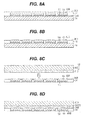
- the second main surface 30B side of the reflective layer 30 is polished or ground. Specifically, by polishing or grinding and thus removing the reflective layer 30 which is formed so as to cover the second main surfaces 40B of the wiring patterns 40, the second main surfaces 40B of the wiring patterns 40 are exposed from the reflective layer 30.
- the second main surface 30B of the reflective layer 30 is polished or ground until the second main surfaces 40B of the wiring patterns 40 are exposed.
- the polishing may use, for example, buff grinding.
- a processing rate is different depending on malleability of a material to be processed. Specifically, in the buff grinding, a processing rate is great in a material having the relatively high brittleness (a cured resin or the like), and a processing rate is small in a material (for example, metal) having the relatively low brittleness.
- the second main surface 30B side of the reflective layer 30 is buff-polished until the second main surfaces 40B of the wiring patterns 40 are reliably exposed, the second main surfaces 40B of the wiring patterns 40 are exposed from the reflective layer 30 so as to rise like a mountain due to the difference between the processing rates as described above, as shown in Fig. 8B .
- the structure 22 where the insulating layer 21 is adhered to the substrate 10A is disposed over the structure after the removal as shown in Fig. 8C .
- the sheet-shaped structure 22 is formed on the second main surface 30B of the reflective layer 30 and the second main surfaces 40B of the wiring patterns 40 through thermocompression.
- the wiring patterns 40 exposed from the reflective layer 30 are pushed into the insulating layer 21.
- the entire second main surface 30B of the reflective layer 30 and the entire second main surfaces 40B of the wiring patterns 40 are covered with the insulating layer 21.
- the insulating layer 21 is cured in an atmosphere of a temperature of about 150°C, thereby forming the insulating layer 20.
- the wiring patterns 40 directly come into contact with the insulating layer 20 which is made of a material with high heat conductivity. For this reason, heat generated by the light emitting element 60 can be conducted to the insulating layer 20 from the wiring patterns 40 with efficiency, and heat generated by the light emitting element 60 can be conducted to the heat sink 10 with efficiency. Therefore, it is possible to improve heat dissipation performance of the light emitting device 2. As a result, since temperature of the light emitting element 60 can be suppressed from increasing, it is possible to appropriately suppress reduction in emission efficiency of the light emitting element 60.
- the second main surfaces 40B of the wiring patterns 40 are exposed from the reflective layer 30 through the buff grinding as described above, the second main surfaces 40B of the wiring patterns 40 are formed in a mountain shape. For this reason, it is possible to increase the contact area between the wiring patterns 40 and the insulating layer 20 as compared with a case where the second main surfaces 40B of the wiring patterns 40 are planarized surfaces. Thereby, it is possible to increase a heat conduction amount from the wiring patterns 40 to the insulating layer 20 and to thereby conduct heat generated by the light emitting element 60 to the heat sink 10 with efficiency. Therefore, it is possible to further improve the heat dissipation performance of the light emitting device 2.
- polishing or grinding is not limited to the buff grinding, and, for example, a blast process, byte grinding where grinding is performed using a grinding edge (tool) made of tungsten carbide or diamond, or the like, may be used.
- a blast process byte grinding where grinding is performed using a grinding edge (tool) made of tungsten carbide or diamond, or the like, may be used.
- the supporting substrate 70 formed of a copper plate is used as a temporary substrate in the manufacturing steps.
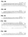
- the present invention is not limited thereto, and, as shown in Fig. 9A , metal foil with a carrier where a very thin metal foil 82 is formed on one surface side of a carrier layer 81 via a release sheet (peeling layer) (not shown) may be used as a supporting substrate 80 instead of the supporting substrate 70.
- the metal foil 82 may use a copper foil.
- the thickness of the metal foil 82 may be, for example, about 1 ⁇ m to 5 ⁇ m.
- As a material of the carrier layer 81 for example, copper or a copper alloy may be used.
- the carrier layer 81 is thicker than the metal foil 82, and the thickness thereof may be, for example, about 30 ⁇ m to 50 ⁇ m.
- the carrier layer 81 functions as a supporting member for securing the mechanical strength of the structure in the manufacturing steps, and also functions as a member for carrying the metal foil 82 which is difficult to handle.
- a release sheet interposed between the carrier layer 81 and the metal foil 82 for example, a silicon release sheet or a fluorine release sheet may be used.
- the carrier layer 81 is mechanically peeled, and thereby a structure where the metal layers 50, the wiring patterns 40, the reflective layer 30 covering them are formed on the first main surface 82A of the metal foil 82 is obtained, as shown in Fig. 9B .
- the metal foil 82 is removed through wet etching or the like, thereby removing the supporting substrate 80 from the structure shown in Fig. 9A as shown in Fig. 9C . If the supporting substrate 80 is used, most (the carrier layer 81) of the supporting substrate 80 can be peeled mechanically, and thus it is possible to reduce time required for chemical removal such as wet etching. Further, it is possible to reduce time for removing the entire supporting substrate 80 and to thereby contribute to cost reduction.
- a structure where a very thin metal foil 82 is formed on one surface side of a carrier layer 81 via a release sheet (peeling layer) (not shown) and a core substrate 83 is formed on the other surface side of the carrier layer 81 may be used as a supporting substrate 80A instead of the supporting substrate 70.
- a material of the core substrate 83 for example, a glass epoxy resin or the like may be used.
- the thickness of the core substrate 83 may be, for example, about 0.5 mm to 2.0 mm.
- the core substrate 83 and the carrier layer 81 are mechanically peeled, and thereby a structure where the metal layers 50, the wiring patterns 40, the reflective layer 30 covering them are formed on the first main surface 82A of the metal foil 82 is obtained, as shown in Fig. 10B .
- the metal foil 82 is removed through wet etching or the like, thereby removing the supporting substrate 80A from the structure shown in Fig. 10A . If the supporting substrate 80A is used, most (the carrier layer 81 and the core substrate 83) of the supporting substrate 80A can be peeled mechanically, and thus it is possible to reduce time for removing the entire supporting substrate 80A. Further, it is possible to improve the mechanical strength of the structure of the manufacturing steps by the core substrate 83.
- the supporting substrate 70 is removed after forming the reflective layer 30 which covers the metal layers 50 and the wiring patterns 40 on the first main surface 70A of the supporting substrate 70.
- the supporting substrate 70 may be removed after forming a structure corresponding to the wiring substrate 1 on the first main surface 70A of the supporting substrate 70.
- the reflective layer 30 is relatively thick (for example, 50 ⁇ m or more)
- the structure 22 can be easily formed.
- the reflective layer 30 is relatively thin (for example, about 20 ⁇ m to 40 ⁇ m)
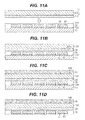
- the mechanical strength of a structure (the structure shown in Fig. 6A ) after removing the supporting substrate 70 is insufficient, and thus the structure 22 cannot be stably formed. Therefore, as shown in Fig. 11 , after the metal layers 50, the wiring patterns 40, and the reflective layer 30 covering them are formed on the first main surface 70A of the supporting substrate 70, the structure 22 may be formed without removing the supporting substrate 70.
- the structure 22 formed of the substrate 10A and the insulating layer 21 is disposed over the structure shown in Fig. 5C .
- the sheet-shaped structure 22 is formed on the second main surface 30B of the reflective layer 30 through thermocompression and is cured. Thereby, the insulating layer 20 and the substrate 10A are formed on the second main surface 30B of the reflective layer 30.
- a resist layer 85 which covers the entire first main surface 10B (the upper surface in Fig. 11C ) of the substrate 10A is formed.
- the thickness of the resist layer 85 is sufficient as long as the resist layer 85 covers the entire first main surface 10B so as to prevent the first main surface 10B of the substrate 10A from being etched in the subsequent step, and may be, for example, about 0.02 mm to 0.05 mm.
- an etching resistant material may be used as a material of the resist layer 85.
- a photosensitive dry film resist, a liquid photoresist for example, a dry film resist or a liquid resist of a Novolac resin, an acryl resin, or the like
- a photoresist for example, a dry film resist or a liquid resist of a Novolac resin, an acryl resin, or the like
- the supporting substrate 70 (refer to Fig. 11C ) which is used as a temporary substrate is removed. Thereafter, the resist layer 85 is removed by, for example, an alkaline stripping agent, and thereby a structure corresponding to the wiring substrate 1 is formed in each wiring substrate forming region C1 of the substrate 10A.
- the resist layer 85 is formed before removing the supporting substrate 70
- formation of the resist layer 85 may be omitted.
- the thickness of the metal foil 82 which is removed chemically through wet etching or the like is very small (about 1 ⁇ m to 5 ⁇ m)
- the heat sink 10 is removed only by an extent of several % of the overall thickness even if forming of the resist layer 85 is omitted in this case. For this reason, forming of the resist layer 85 can be omitted in this case.
- the resist layer 71 having the openings 71X is formed on the first main surface 70A of the supporting substrate 70, the metal layers 50 and the wiring patterns 40 are formed on the first main surface 70A exposed from the openings 71X, and then the reflective layer 30 which covers the metal layers 50 and the wiring patterns 40 is formed.
- the present invention is not limited thereto, and, for example, a reflective layer having openings with the same shape as the openings 71X may be formed on the first main surface 70A of the supporting substrate 70, and the metal layers 50 and the wiring patterns 40 may be formed on the first main surface 70A exposed from the openings of the reflective layer.
- a material of the reflective layer in this case is required to have plating resistance.
- the insulating layer 20 in the above-described embodiment may be omitted.
- the wiring substrate may be manufactured according to, for example, the following manufacturing method. Specifically, as shown in Fig. 12A , a structure 32A where a sheet-shape reflective layer 32 is adhered to the substrate 10A is disposed over a structure where the metal layers 50 and the wiring patterns 40 are formed on the first main surface 70A of the supporting substrate 70. At this time, the structure 32A is disposed in a state where the reflective layer 32 faces downward such that the reflective layer 32 faces the wiring patterns 40 and the supporting substrate 70.
- a white insulating resin which has high reflectance and a thermosetting property may be used.
- a material of the reflective layer 32 is preferably an insulating resin having the high heat conductivity from the viewpoint of heat dissipation.
- the white insulating resin for example, a resin material where a filler or a pigment formed from white titanium oxide or barium sulfate is contained in an epoxy resin or a silicon resin may be used.
- the reflective layer 32 uses one in a B-stage state.
- the thickness of the reflective layer 32 may be a thickness capable of covering, for example, the metal layers 50 and the wiring patterns 40, and may be, for example, about 20 ⁇ m to 130 ⁇ m.
- the sheet-shaped structure 32A is formed on the first main surface 70A of the supporting substrate 70 through thermocompression.
- the thermocompression at this time as shown in Fig. 12B , the wiring patterns 40 and the metal layers 50 are pushed into the reflective layer 32.
- the first main surface 70A of the supporting substrate 70, the entire side surfaces of the wiring patterns 40, the entire side surfaces of the metal layers 50, and the entire second main surfaces 40B of the wiring patterns 40 are covered with the reflective layer 32.
- the reflective layer 32 is cured by performing a heat curing treatment in an atmosphere of a temperature of about 150°C, thereby forming a reflective layer 33.
- recessed portions 34 which accommodate the wiring patterns 40 and the metal layers 50 are formed in the first main surface 33A of the reflective layer 33, and the wiring patterns 40 are formed on the bottom surfaces 34A of the recessed portions 34.
- the wiring patterns 40 and the metal layers 50 are pushed in the reflective layer 32, and the reflective layer 33 which covers the wiring patterns 40 and the metal layers 50 is formed. For this reason, according to the manufacturing method, even if a gap between the wiring patterns 40 and a gap between the metal layers 50 are narrowed, the reflective layer 33 can be easily formed between the wiring patterns 40 and between the metal layers 50.
- the reflective layer 32 is formed in the vacuum atmosphere, and thereby it is possible to suppress void from being involved into the reflective layer 32.
- the supporting substrate 70 is removed through etching, the substrate 10A and the like are cut along the cutting lines D1 so as to be generated as a unit piece, and thereby a wiring substrate 1A as shown in Fig. 12C can be obtained.
- the first main surface 33A (the outermost surface) of the reflective layer 33 which is formed on the outermost surface of the mounting surface side of the light emitting element 60 is formed so as to be flush with the first main surfaces (the outermost surfaces) 50A of the metal layers 50.
- the insulating layer 20 is omitted, and thus the reflective layer 33 has functions of adhering the heat sink 10 to the wiring patterns 40 and of insulating the heat sink 10 from the wiring patterns 40.
- the resin layer interposed between the wiring patterns 40 and the heat sink 10 can be made to be thin, and thus it is possible to improve a heat dissipation performance.
- the reflective layer 33 may be formed so as to cover the metal layers 50 and the wiring patterns 40 formed on the first main surface 70A of the supporting substrate 70, and the substrate 10A may be formed on the reflective layer 33.
- the reflective layer 33 is formed so as to cover the entire side surfaces of the metal layers 50, the entire surfaces of the wiring patterns 40, and the entire second main surfaces 40B of the wiring patterns 40.
- the first main surface 33A (the outermost surface) of the reflective layer 33 which is formed on the outermost surface of the mounting surface side of the light emitting element 60 is formed so as to be flush with the first main surfaces (the outermost surfaces) 50A of the metal layers 50.
- the wiring substrate having the same structure as that of the wiring substrate 1A shown in Fig. 12C .
- the reflective layer 33 in this case may be formed according to, for example, a screen printing method or a roll covering method using a resin paste.
- the structure 32A where the sheet-shaped reflective layer 32 made of the same material as that of the reflective layer 30 is adhered to the substrate 10A may be formed on a structure where the reflective layer 30 covering the metal layers 50 and the wiring patterns 40 is formed on the first main surface 70A of the supporting substrate 70.
- the sheet-shaped structure 32A is formed on the second main surface 30B of the reflective layer 30 through thermocompression. Thereby, the reflective layer 32 and the substrate 10A are formed on the second main surface 30B of the reflective layer 30. Thereafter, the reflective layer 32 is cured by performing a heat curing treatment in an atmosphere of a temperature of about 150°C, thereby forming the reflective layer 33.
- Even in the structure and the manufacturing method it is possible to achieve the same effects as in (1) to (5) of the first embodiment.
- the sheet-shaped insulating resin is used as a material of the insulating layer 21 which becomes the insulating layer 20
- a liquid or paste insulating resin may be used as a material of the insulating layer 21.
- the sheet-shaped insulating resin is used as a material of the reflective layer 32 which becomes the reflective layer 33
- a liquid or paste insulating resin may be used as a material of the reflective layer 32.
- the wiring substrate 1 is formed as a unit piece, and then the light emitting element 60 is mounted on the pads 50P of the wiring substrate 1.
- the present invention is not limited thereto, and, as shown in Fig. 15 , the light emitting element 60 may be mounted on the pads 50P before the wiring substrate 1 is formed as a unit piece, and then cutting may be performed along the cutting lines D1, thereby obtaining each light emitting device 2.
- the light emitting element 60 is mounted on the pads 50P as shown in Fig. 15B without cutting along the cutting lines D1.
- Fig. 15A after the insulating layer 20 and the substrate 10A are formed on the second main surface 30B of the reflective layer 30, the light emitting element 60 is mounted on the pads 50P as shown in Fig. 15B without cutting along the cutting lines D1.
- Fig. 15A after the insulating layer 20 and the substrate 10A are formed on the second main surface 30B of the reflective layer 30, the light emitting element 60 is mounted on the pads 50P as shown in Fig. 15B without cutting along the
- the structure shown in the same figure is shown so as to be vertically reverse to that shown in Fig. 15A .
- Fig. 15C after the light emitting elements 60 are encapsulated with the encapsulating resin 65, cutting may be performed along the cutting lines D1, thereby obtaining each light emitting device 2 as shown in Fig. 15D .
- the encapsulating resin 65 may be formed for the respective partitions where the wiring substrate forming regions C1 are formed in a matrix (in Fig. 3 , 3x3) using a collective molding method, or may be formed for each wiring substrate forming region C1 using a separate molding method.
- the reflective layer 30 is formed using the screen printing method.
- the present invention is not limited thereto, and, for example, the reflective layer 30 may be formed using a roll covering method.
- the reflective layer 30 may be formed by applying a liquid resin using a dispenser.
- one bump 61 is flip-chip bonded to one pad 50P of the two pads 50P formed in each mounting region CA, and the other bump 61 is flip-chip bonded to the other pad 50P.
- the present invention is not limited thereto, and, for example, a plurality of bumps 61 may be flip-chip bonded to one pad 50P, and a plurality of bumps 61 may be flip-chip bonded to the other pad 50P.
- a connection location on each pad 50P is only one, and thus there is concern that the light emitting element 60 mounted on the wiring substrate 1 may be tilted.
- a plurality of bumps 61 are bonded to a single pad 50P, and thus there are a plurality of connection locations on each pad 50P. Thereby, it is possible to stably mount the light emitting element 60 on the wiring substrate 1.
- a plurality of light emitting elements 60 mounted on the wiring substrate 1 are collectively encapsulated with the encapsulating resin 65.
- the present invention is not limited thereto, and the light emitting element 60 mounted in each mounting region CA may be encapsulated separately with an encapsulating resin.
- a shape of the mounting region CA and the terminal region TA in the above-described embodiment is not limited to a circular shape, and may be, for example, a polygonal shape such as a rectangular shape or a pentagonal shape, a semi-circular shape, an elliptical shape, or a semi-elliptical shape.
- the above-described embodiment is implemented using the multi-piece manufacturing method, but may be implemented using a single-piece manufacturing method.
- a base material a supporting substrate or a heat sink
- the wiring substrate 1 and the light emitting device 2 may be manufactured.
- a planar shape of each of the wiring substrate 1 and the light emitting device 2 in the above-described embodiment is not limited to a rectangular shape, and may be, for example, a polygonal shape such as a triangular shape or a pentagonal shape, or a circular shape.
- the number or arrangement of the light emitting elements 60 mounted on the wiring substrate 1 in the above-described embodiment is not particularly limited.
- a shape of the wiring pattern 40 and the metal layer 50 in the above-described embodiment is not particularly limited.
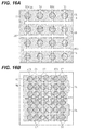
- a modification to a metal layer with a pattern as shown in Fig. 16A may be disposed in an approximately W shape in plan view.
- a groove-shape opening 55X extending in the vertical direction of the figure is formed between the metal layers 55 which are adjacent to each other in the horizontal direction of the figure.
- a strip-shaped opening 55Y extending in the horizontal direction of the figure is formed between the metal layers 55 which are adjacent to each other in the vertical direction of the figure.
- a plurality of metal layers 55 are separated from each other by the openings 55X and 55Y.
- the metal layers 55 have mounting regions CA arranged in a matrix (here, 4x4).
- the metal layers 55 have a pair of terminal regions TA functioning as electrode terminals.
- the pair of terminal regions TA are respectively formed on the metal layers 55 which are positioned at the start point and end point of the W shape among a plurality of metal layers 55 arranged in an approximately W shape.
- a plurality of (here, sixteen) light emitting elements are connected in series between one terminal region TA and the other terminal region TA.
- a metal layer 56 with an approximately strip shape in plan view may be disposed, and a plurality of metal layers 57 with an approximately rectangular shape in plan view, disposed in parallel to the metal layer 56 so as to be adjacent to each other, may be disposed in a matrix (in this embodiment, matrix of 6x2). That is, the metal layer 56 is commonly provided with respect to the adjacent metal layers 57 of two rows.
- groove-shaped openings 57X extending in the vertical direction of the figure are formed between the metal layers 56 and 57 and between the respective metal layers 57 which are adjacent to each other in the horizontal direction of the figure.
- strip-shaped openings 57Y extending in the horizontal direction of the figure are formed between the metal layers 57 which are adjacent to each other in the vertical direction of the figure.
- the metal layers 56 and 57, and the metal layers 57 are respectively separated from each other by the openings 57X and 57Y.
- the metal layers 56 and 57 have mounting regions CA arranged in a matrix (in this embodiment, matrix of 6x6).
- the metal layers 57 have a pair of terminal regions TA functioning as electrode terminals.
- the pair of terminal regions TA are formed in two metal layers 57 which is the farthest from the metal layer 56.
- the light emitting elements arranged in a matrix are connected in series and in parallel between the metal layer 56 and one terminal region TA.
- the light emitting elements arranged in a matrix are connected in series and in parallel between the metal layer 56 and the other terminal region TA.
- the light emitting element groups connected in series and in parallel are connected in series.
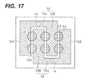
- a pair of metal layers 58 with an approximately comb shape in plan view may be formed.
- the metal layer 58 has an electrode portion 58A which is formed in a rectangular shape in plan view and has a terminal region TA, and a plurality of (in Fig. 17 , two) extending portions 58B with a comb-teeth shape extending inward from the electrode portion 58A.
- the pair of metal layers 58 are disposed such that the mutual extending portions 58B are alternately arranged.
- an opening 58X with an approximately Z shape in plan view is formed between the metal layers 58.
- the pair of metal layers 58 are separated from each other by the opening 58X.
- the metal layers 58 have mounting regions CA arranged in a matrix (in this embodiment, matrix of 3x2).
- each light emitting element 60 is flip-chip mounted on the extending portions 58B (the metal layers 58) formed on both the sides of the opening 58X in each of the mounting regions CA so as to cross over the opening 58X.
- a plurality of light emitting elements 60 are connected in series and in parallel between one terminal region TA and the other terminal region TA.
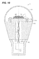
- Fig. 18 shows a cross-sectional view when the light emitting device 2 according to the embodiment is applied to an illumination apparatus 3.
- the illumination apparatus 3 includes the light emitting device 2, a mounting board 100 having the light emitting device 2 mounted thereon, and an apparatus main body 120 in which the mounting board 100 is installed.
- the illumination apparatus 3 includes a cover 130 which is installed in the apparatus main body 120 and covers the light emitting device 2, a holder 140 which holds the apparatus main body 120, and a lighting circuit 150 which is fitted to the holder 140 and turns on the light emitting elements 60.
- the apparatus main body 120 is formed in an approximately truncated conical shape in plan view.
- the apparatus main body 120 has a cross section 120A with a large diameter in which the mounting board 100 and the cover 130 are installed, and a cross section 120B with a small diameter.
- the apparatus main body 120 is made of, for example, aluminum or the like having good heat conductivity.
- the mounting board 100 is installed in the cross section 120A of the apparatus main body 120 using well-known installation means (in this embodiment, screws).
- the apparatus main body 120 is provided with a through-hole 120X which penetrates between the cross section 120A and the cross section 120B.
- Wires 160 which are electrically connected to the light emitting elements 60 of the light emitting device 2 via the mounting board 100 are disposed in the through-hole 120X.
- the wires 160 are lead to the cross section 120B side from the cross section 120A side via the through-hole 120X.
- the cover 130 formed in an approximately dome shape in exterior view is fixed to the cross section 120A of the apparatus main body 120 by an adhesive such as a silicon resin such that the inside of the cover 130 is in an airtight state.
- the cover 130 is made of, for example, hard glass.
- the holder 140 is made of, for example, a polybutylene terephthalate (PBT) resin or a polyethersulfone (PES) resin.
- the holder 140 is installed in the cross section 120B of the apparatus main body 120 using well-known installation means (an adhesive, a screw, or the like).
- a socket (not shown) is fitted to the holder 140.
- the lighting circuit 150 is accommodated inside the holder 140 and the socket.
- a circuit board (not shown) of the lighting circuit 150 on which circuit components are mounted is attached to the holder 140.
- the lighting circuit 150 is a circuit which converts an AC voltage supplied from the socket into a DC voltage, and supplies the DC voltage to the light emitting elements 60 via the wires 160 such that the light emitting elements 60 emit light.
- Fig. 19A shows a cross-sectional view when the light emitting device 2 is mounted on a mounting board 100A.
- the mounting board 100A includes a metal plate 101, an insulating layer 102 formed on the upper surface of the metal plate 101, and a wiring pattern 103 formed on the upper surface of the insulating layer 102.
- a metal with favorable heat conductivity such as, for example, aluminum and copper may be used.
- a material of the insulating layer 102 for example, an insulating resin such as a polyimide resin or an epoxy resin, or a resin material where a filler such as silica or alumina is mixed with the resin may be used.
- a material of the wiring pattern 103 for example, copper or a copper alloy may be used.
- An opening 102X which exposes a part of the metal plate 101 as a mounting region of the light emitting device 2 is formed in the insulating layer 102.
- the light emitting device 2 is mounted in the mounting region, that is, on the metal plate 101 exposed from the opening 102X.
- the heat sink 10 formed on the lower surface thereof is thermally bonded onto the metal plate 101 by a heat conduction member 104.
- the heat conduction member 104 may use, for example, a heat conduction member where a high heat conductivity substance such as, for example, indium (In), silicon (or hydrogen carbide) grease, a metal filler, or a graphite is produced in a sheet form with a resin binder.
- the metal layers 50 of the terminal regions TA of the light emitting device 2 mounted on the mounting board 100A are electrically connected to the wiring patterns 103 of the mounting board 100A via spring-like connection terminals 105 (in this embodiment, lead pins).
- the heat sink 10 of the light emitting device 2 is bonded onto the metal plate 101 of the mounting board 100A, heat generated from the light emitting device 2 can be dissipated to the metal plate 101.
- Fig. 19B shows a cross-sectional view illustrating a state that the light emitting device 2 is mounted on a mounting board 100B.
- the mounting board 100B includes a metal plate 111, an insulating layer 112 formed on the upper surface of the metal plate 111, and a wiring pattern 113 formed on the upper surface of the insulating layer 112.
- a metal with favorable heat conductivity such as, for example, aluminum and copper may be used.
- an insulating resin such as a polyimide resin or an epoxy resin, or a resin material where a filler such as silica or alumina is mixed with the resin may be used.
- a material of the wiring pattern 113 for example, copper or a copper alloy may be used.
- the light emitting device 2 is mounted on the wiring pattern 113.
- the heat sink 10 formed on the lower surface thereof is thermally bonded onto the wiring pattern 113 by a heat conduction member 114.
- the heat conduction member 114 may use, for example, a heat conduction member where a high heat conductivity substance such as, for example, indium, silicon (or hydrogen carbide) grease, a metal filler, or a graphite is formed in a sheet shape with a resin binder.
- the metal layers 50 of the terminal regions TA of the light emitting device 2 mounted on the mounting board 100B are electrically connected to the wiring patterns 113 of the mounting board 100B via bonding wires 115.
- the heat sink 10 of the light emitting device 2 is thermally bonded to the wiring pattern 113 via the heat conduction member 114, heat generated from the light emitting device 2 can be dissipated to the metal plate 111 from the heat sink 10 via the wiring pattern 113 and the insulating layer 112.
- the wiring pattern 113 which is thermally bonded to the heat sink 10 of the wiring patterns 113 functions as a wiring layer for heat dissipation.
- an opening for exposing the metal plate 111 is not formed in the insulating layer 112; however, in a case where the insulating layer 112 is thin, heat generated from the light emitting device 2 can be dissipated to the metal plate 111 via the insulating layer 112.
- a wiring substrate 1 comprises a heat sink 10; an insulating member 20, 30 on the heat sink; a wiring pattern 40 embedded in the insulating member and comprising a first surface 40A and a second surface 40B opposite to the first surface, the second surface contacting the insulating member; and a metal layer 50 on the first surface of the wiring pattern, wherein a surface 50A of the metal layer is flush with an exposed surface 30A of the insulating member.
- the insulating member comprises an insulating layer 20 directly on the heat sink; and a reflective layer 30 on the insulating layer to cover the second surface of the wiring pattern.
- the insulating member is an insulating layer 20, 33 directly formed on the heat sink to cover the second surface 40B of the wiring pattern 40.
- a heat conductivity of the insulating layer 20 may be higher than that of the reflective layer 30.
- the insulating member is a reflective layer 33 directly formed on the heat sink to cover the second surface 40B of the wiring pattern 40.
- a light emitting device 2 comprises a wiring substrate 1 as described above; a light emitting element 60 mounted on the wiring substrate; and an encapsulating resin 65 that encapsulates the light emitting element.
- a method of manufacturing a wiring substrate 1 comprises:
- the reflective layer 30 comprises a first surface 30A contacting the supporting substrate and a second surface 30B opposite to the first surface, wherein the method further comprises: (e) thinning the reflective layer from the second surface 30B toward the first surface 30A such that the wiring pattern 40 is exposed from the reflective layer.
- the method according to embodiments may further comprise: (f) providing an insulating layer 20 on the reflective layer 30 and providing a heat sink 10 on the insulating layer, wherein a heat conductivity of the insulating layer is higher than that of the reflective layer.
- the method above may further comprise: providing an insulating layer 20 on the reflective layer 30, the method further comprising: (g) providing a heat sink 10 on the reflective layer 30 or on the insulating layer.
- the step (c) above comprises: i) disposing a heat sink on which a semi-cured insulating resin is formed on the supporting substrate such that the semi-cured insulating resin faces the supporting substrate; and ii) completely curing the semi-cured insulating resin to form the reflective layer 30.
- the supporting substrate 70 may comprise a metal foil thereon, and the metal layer may be formed on the supporting substrate via the metal foil.
Landscapes
- Engineering & Computer Science (AREA)
- Manufacturing & Machinery (AREA)
- Microelectronics & Electronic Packaging (AREA)
- Led Device Packages (AREA)
- Led Devices (AREA)
Abstract
Description
- The present disclosure relates to a wiring substrate, a light emitting device, and a manufacturing method of the wiring substrate.
- In the related art, various shapes of light emitting devices in which light emitting elements are mounted on a substrate, have been proposed. As this kind of light emitting device, a structure is known in which wiring layers are formed on an insulating layer formed on a substrate made of metal, and a light emitting element such as a light emitting diode (LED) is mounted on the wiring layers (for example, see
JP-A-2003-092011 - In recent years, the usage of the light emitting device has been expanded to an illumination apparatus, a display apparatus, and the like. For this usage, a plurality of light emitting elements are preferably mounted with high density. In order to satisfy this demand, miniaturization of the light emitting element has been developed. Along with the miniaturization, miniaturization of bumps used to mount the light emitting element in a flip-chip form on the wiring layers has been developed, and thus a gap between the light emitting element and the wiring layers becomes narrowed. On the other hand, in a recent light emitting device, in order to efficiently use light emitted by the light emitting element, a reflective layer having high reflectance is formed on an element mounting surface. However, if the reflective layer is formed, there is a problem in that the reflective layer and the fine light emitting element tend to interfere (contact) with each other. For this reason, it is desirable to develop a light emitting device which can suppress interference between the reflective layer and the light emitting element and mount the fine light emitting element stably thereon.
- Exemplary embodiments of the present invention address the above disadvantages and other disadvantages not described above. However, the present invention is not required to overcome the disadvantages described above, and thus, an exemplary embodiment of the present invention may not overcome any disadvantages described above.
- According to one or more illustrative aspects of the present invention, there is provided a wiring substrate. The wiring substrate includes: a heat sink; an insulating member on the heat sink; a wiring pattern embedded in the insulating member and including a first surface and a second surface opposite to the first surface, the second surface contacting the insulating member; and a metal layer on the first surface of the wiring pattern, wherein a surface of the metal layer is flush with an exposed surface of the insulating member.
- According to the aspect of the present invention, it is possible to provide a wiring substrate capable of suppressing interference between the reflective layer and the light emitting element and accommodating the miniaturization of the light emitting element.
- Other aspects and advantages of the present invention will be apparent from the following description, the drawings and the claims.
-
-
Fig. 1A is a schematic plan view illustrating a wiring substrate according to an embodiment; -
Fig. 1B is a schematic cross-sectional view taken along the line A-A of the wiring substrate shown inFig. 1A ; -
Fig. 2A is a schematic plan view illustrating a light emitting device according to an embodiment; -
Fig. 2B is a schematic cross-sectional view taken along the line B-B of the light emitting device shown inFig. 2A ; -
Fig. 3 is a schematic plan view illustrating a manufacturing method of the wiring substrate according to an embodiment; -
Figs. 4A, 4B and 4D are schematic cross-sectional views illustrating manufacturing steps of the wiring substrate according to the embodiment; -
Fig. 4C is a schematic plan view illustrating the manufacturing steps of the wiring substrate according to the embodiment, whereinFigs. 4A, 4B and 4D show a cross-sectional view of the wiring substrate taken along the line C-C position ofFig. 4C ; -
Figs. 5A and 5C are schematic cross-sectional views illustrating the manufacturing steps of the wiring substrate according to the embodiment; -
Fig. 5B is a schematic plan view illustrating the manufacturing steps of the wiring substrate according to the embodiment, whereinFigs. 5A and 5C show a cross-sectional view of the wiring substrate taken along the line D-D position ofFig. 5B ; -
Figs. 6A to 6D are schematic cross-sectional views illustrating the manufacturing steps of the wiring substrate according to the embodiment, whereinFigs. 6A to 6D show a cross-sectional view of the wiring substrate taken along the line D-D position ofFig. 5B ; -
Figs. 7A and 7B are schematic cross-sectional views illustrating the manufacturing steps of the wiring substrate according to the embodiment, whereinFigs. 7A and 7B show a cross-sectional view of the light emitting device taken along the line B-B position ofFig. 2A ; -
Figs. 8A to 8D are schematic cross-sectional views illustrating manufacturing steps of a wiring substrate according to a modified example of the embodiment, whereinFigs. 8A to 8D show a cross-sectional view of the wiring substrate taken along the line D-D position ofFig. 5B ; -
Figs. 9A to 9C are schematic cross-sectional views illustrating manufacturing steps of a wiring substrate according to a modified example of the embodiment, whereinFigs. 9A to 9C show a cross-sectional view of the wiring substrate taken along the line D-D position ofFig. 5B ; -
Figs. 10A and 10B are schematic cross-sectional views illustrating manufacturing steps of a wiring substrate according to a modified example of the embodiment, whereinFigs. 10A and 10B show a cross-sectional view of the wiring substrate taken along the line D-D position ofFig. 5B ; -
Figs. 11A to 11D are schematic cross-sectional views illustrating manufacturing steps of a wiring substrate according to a modified example of the embodiment, whereinFigs. 11A to 11D show a cross-sectional view of the wiring substrate taken along the line D-D position ofFig. 5B ; -
Figs. 12A to 12C are schematic cross-sectional views illustrating manufacturing steps of a wiring substrate according to a modified example of the embodiment, whereinFigs. 12A to 12C show a cross-sectional view of the wiring substrate taken along the line D-D position ofFig. 5B ; -
Figs. 13A and 13B are schematic cross-sectional views illustrating manufacturing steps of a wiring substrate according to a modified example of the embodiment, whereinFigs. 13A and 13B show a cross-sectional view of the wiring substrate taken along the line D-D position ofFig. 5B ; -
Figs. 14A and 14B are schematic cross-sectional views illustrating manufacturing steps of a wiring substrate according to a modified example of the embodiment, whereinFigs. 14A and 14B show a cross-sectional view of the wiring substrate taken along the line D-D position ofFig. 5B ; -
Figs. 15A to 15D are schematic cross-sectional views illustrating manufacturing steps of a wiring substrate and a light emitting device according to a modified example of the embodiment, whereinFigs. 15A to 15D show a cross-sectional view of the wiring substrate and the light emitting device taken along the line D-D position ofFig. 5B ; -
Figs. 16A and 16B are schematic plan views illustrating a metal layer according to a modified example of the embodiment; -
Fig. 17 is a schematic plan view illustrating a metal layer according to a modified example of the embodiment; -
Fig. 18 is a schematic cross-sectional view illustrating an application example of the light emitting device; and -
Figs. 19A and 19B are schematic cross-sectional views illustrating a mounting example of the light emitting device. - Hereinafter, exemplary embodiments of the present invention will be described with reference to the accompanying drawings. In all the drawings for the explanation of the embodiments, the members having the same functions are represented by the same reference numerals, and repeated description thereof will be omitted.
- In addition, for convenience, in the accompanying drawings, there are cases in which featured portions are shown appropriately enlarged to easily understand features thereof, and the dimensions of each constituent element may be different from practical dimensions thereof. Further, in a cross-sectional view, hatching of some members is omitted in order to easily understand a cross-sectional view of each member.
- The embodiments described in the following also illustrate various aspects of the invention in more detail. Each one of the aspects of any embodiment may be combined with any other aspect or aspects unless clearly indicated to the contrary.
- Hereinafter, the first embodiment will be described with reference to
Figs. 1 to 7 . - As shown in
Fig. 1B , awiring substrate 1 includes aheat sink 10, an insulatinglayer 20 covering the upper surface of theheat sink 10, areflective layer 30 formed on the insulatinglayer 20,wiring patterns 40 embedded in thereflective layer 30, andmetal layers 50 formed on thewiring patterns 40. Thiswiring substrate 1 is a wiring substrate applied to, for example, a light emitting device. - The
heat sink 10 is, for example, an approximately rectangular thin plate in plan view. As a material of theheat sink 10, for example, a metal with favorable heat conductivity such as copper (Cu) or aluminum (Al), or an alloy including at least one of these metals may be used. In addition, as a material of theheat sink 10, for example, a ceramic material with favorable heat conductivity such as aluminum nitride or alumina may be used. The thickness of theheat sink 10 may be, for example, about 0.5 mm to 1.0 mm. - The insulating
layer 20 is formed so as to cover the entire upper surface of theheat sink 10. As a material of the insulatinglayer 20, for example, an insulating resin with high heat conductivity (for example, about 1 W/mK to 10 W/mK) may be used. Specifically, as a material of the insulatinglayer 20, for example, an insulating resin such as a polyimide resin or an epoxy resin, or a resin material where a filler such as silica or alumina is mixed with the resin may be used. The thickness of the insulatinglayer 20 may be, for example, about 50 µm to 80 µm. The insulatinglayer 20 has a function of insulating theheat sink 10 from thewiring patterns 40, and a function of adhering theheat sink 10 to thereflective layer 30. Further, in a case where the insulatinglayer 20 has high insulation properties, the insulatinglayer 20 is preferably formed thinly from the viewpoint of heat dissipation. - The
reflective layer 30 is formed so as to cover the entire firstmain surface 20A of the insulatinglayer 20. Thereflective layer 30 has high reflectance. Specifically, thereflective layer 30 has reflectance of 50% or more (preferably, 80% or more) between the wavelength 450 nm to 700 nm. Thereflective layer 30 is also referred to as a white resist layer. As a material of thereflective layer 30, for example, a white insulating resin may be used. As the white insulating resin, for example, a resin material where a filler or a pigment formed from white titanium oxide (TiO2) or barium sulfate (BaSO4) is contained in an epoxy resin, a silicon resin, or an organopolysiloxane resin. The reflective layer 30 (white resist layers) covers the outermost surface of thewiring substrate 1, and thereby it is possible to reduce light amount loss of light emitting elements by increasing the reflectance of light from the light emitting elements mounted on thewiring substrate 1 as well as protecting thewiring patterns 40. In addition, the thickness of thereflective layer 30 may be, for example, 20 µm to 130 µm. - In addition, in the first
main surface 30A (the upper surface inFig. 1B ) of thereflective layer 30, recessedportions 31 are formed at necessary locations (Fig. 1B , five). Each of the recessedportions 31 is formed from the firstmain surface 30A of thereflective layer 30 to a middle position of thereflective layer 30 in the thickness direction. That is, each of the recessedportions 31 is formed such that the bottom surface 31A of the recessedportion 31 is positioned in the middle of thereflective layer 30 in the thickness direction. As shown inFig. 1A , a planar shape of the recessedportion 31 is formed in a strip shape in plan view or in a rectangular shape in plan view. In addition, the plurality of recessedportions 31 are formed in parallel so as to be adjacent to each other. - As shown in
Fig. 1B , thewiring patterns 40 are formed on the bottom surfaces 31A of the respective recessedportions 31. The plurality ofwiring patterns 40 are formed in parallel so as to be adjacent to each other. The side surface of eachwiring pattern 40 is covered by thereflective layer 30 forming the side walls of the recessedportions 31. In addition, theadjacent wiring patterns 40 are electrically separated by thereflective layer 30 forming the side walls of the recessedportions 31. As such, thewiring pattern 40 is formed so as to be embedded in thereflective layer 30. In addition, although not shown, a planar shape of eachwiring pattern 40 is formed in a strip shape in plan view or in a rectangular shape in plan view in the same manner as the planar shape of the recessedportion 31. Further, as a material of thewiring pattern 40, for example, copper or a copper alloy may be used. The thickness of thewiring pattern 40 may be, for example, about 30 µm to 100 µm. In addition, the distance between theadjacent wiring patterns 40 may be, for example, about 0.1 mm to 0.3 mm. According to an aspect, thewiring pattern 40 is embedded in the reflective layer in such a manner that at least a substantial portion of its side surface (e.g. more than 50% or even more than 80% of or all of its side surface) is in contact with thereflective layer 30, and that possibly also its bottom surface is in contact with thereflective layer 30. - The
metal layer 50 is formed in the recessedportion 31 so as to cover the entire firstmain surface 40A (the upper surface inFig. 1B ) of eachwiring pattern 40. Specifically, as shown inFig. 1A , a plurality of (inFig. 1A , five) metal layers 50 with a strip shape in plan view (a rectangular shape in plan view) are formed in parallel so as to be adjacent to each other. In addition, theadjacent metal layers 50 are electrically separated by thereflective layer 30 forming the side walls of the recessedportions 31. As shown inFig. 1B , each of the metal layers 50 is formed such that the firstmain surface 50A (the upper surface inFig. 1B ) thereof is flush with the firstmain surface 30A of thereflective layer 30. For this reason, in themetal layer 50, the entire firstmain surface 50A thereof is exposed from thereflective layer 30. Further, as shown inFig. 1A , the metal layers 50 exposed from thereflective layer 30 have a plurality of regions which are mounting regions CA in which light emitting elements 60 (refer toFig. 2 ) are mounted, and have a pair of terminal regions TA functioning as electrode terminals. Here, the mounting regions CA are arranged in a matrix (4x4 inFig. 1A ) on the metal layers 50. In the mounting regions CA, a pair ofmetal layers 50 which are separated by thereflective layer 30 forming the side walls of the recessedportions 31 and are formed with thereflective layer 30 interposed therebetween are exposed to outside. The pair ofmetal layers 50 respectively function aspads 50P to which the light emitting elements 60 (refer toFig. 2 ) are bonded. In addition, a pair of terminal regions TA are disposed on the metal layers 50 to the outside of the mounting regions CA. Specifically, a pair of terminal regions TA are formed on twometal layers 50 disposed at the outermost positions of the fivemetal layers 50 and are formed to the outside of the mounting regions CA disposed in the metal layers 50. - An example of the
metal layer 50 may include a silver (Ag) layer, a nickel (Ni)/gold (Au) layer (a metal layer where an Ni layer and an Au layer are formed in this order), an Ni/Ag layer (a metal layer where an Ni layer and an Ag layer are formed in this order), an Ni/palladium (Pd)/Au layer (a metal layer where an Ni layer, a Pd layer, and an Au layer are formed in this order), or the like. Further, an example of themetal layer 50 may include an Ni/Pd/Ag layer (a metal layer where an Ni layer, a Pd layer, and an Ag layer are formed in this order), an Ni/Pd/Ag/Au layer (an Ni layer, a Pd layer, an Ag layer, and an Au layer are formed in this order), or the like. Furthermore, in a case where themetal layer 50 is, for example, an Ni/Au layer, the thickness of the Ni layer may be about 1 µm to 10 µm, and the thickness of the Au layer may be about 0.05 µm to 2 µm. - Next, a structure of a
light emitting device 2 will be described. - As shown in
Fig. 2B , thelight emitting device 2 includes the above-describedwiring substrate 1, a plurality of (inFig. 2A , sixteen)light emitting elements 60 mounted on thewiring substrate 1, and an encapsulatingresin 65 which encapsulates thelight emitting elements 60 and the like. - Each
light emitting element 60 is mounted on a pair ofpads 50P formed in each mounting region CA of thewiring substrate 1. Specifically, eachlight emitting element 60 is flip-chip mounted on twopads 50P formed on both sides of thereflective layer 30 so as to cross over thereflective layer 30 formed between the pair ofpads 50P, that is, thereflective layer 30 forming the side walls of the recessedportions 31. More specifically, onebump 61 formed on one surface (the lower surface inFig. 2B ) of thelight emitting element 60 is flip-chip bonded to onepad 50P of the twopads 50P, and theother bump 61 is flip-chip bonded to theother pad 50P. Thereby, eachbump 61 of each light emittingelement 60 is electrically connected to thewiring pattern 40 via thepad 50P (the metal layer 50). In addition, as shown inFig. 2A , thelight emitting elements 60 are arranged in a matrix (4x4 inFig. 2A ) on thewiring substrate 1. For this reason, in thelight emitting device 2, between the pair of terminal regions TA, fourlight emitting elements 60 are connected in series, and four groups of the serially connectedlight emitting elements 60 are connected in parallel. In addition, thelight emitting elements 60 are supplied with power from an external power source (not shown) via the metal layers 50 formed in the terminal regions TA or thewiring patterns 40 and emit light. Further, a planar shape of thelight emitting element 60 is formed, for example, in a rectangular shape, and the size thereof may be, for example, about 0.3 mm2 to 0.5 mm2. Furthermore, the height of thebump 61 may be, for example, about 30 µm to 100 µm. - As the
light emitting element 60, for example, a light emitting diode (LED) or a vertical cavity surface emitting laser (VCSEL) may be used. As thebump 61, for example, a gold bump or a solder bump may be used. As a material of the solder bump, for example, an alloy including lead (Pb), an alloy of tin (Sn) and Au, an alloy of Sn and Cu, an alloy of Sn and Ag, an alloy of Sn, Ag and Cu, or the like may be used. - As shown in
Fig. 2B , the encapsulatingresin 65 is provided on the upper surface of thewiring substrate 1 so as to encapsulate thelight emitting elements 60, thebumps 61, and the like. As a material of the encapsulatingresin 65, for example, a resin material where a fluorescent substance is contained in a silicon resin may be used. The resin material containing the fluorescent substance is formed on thelight emitting elements 60, thus a mixed color of emission of thelight emitting element 60 and emission of the fluorescent substance can be used, and thereby it is possible to control various emission colors of thelight emitting device 2. - In the
wiring substrate 1 according to the present embodiment, the firstmain surface 30A (the outermost surface) of thereflective layer 30 formed in the outermost surface of the mounting surface side where thelight emitting element 60 is mounted is formed so as to be flush with the firstmain surface 50A (the outermost surface) of themetal layer 50 functioning as thepad 50P. That is, the surface of thereflective layer 30 is formed so as to be flush with thepad 50P. Thereby, since thereflective layer 30 does not protrude further upward than the surface of thepad 50P, interference (contact) between thereflective layer 30 and thelight emitting element 60 is appropriately suppressed. - Next, a manufacturing method of the
wiring substrate 1 will be described with reference toFigs. 3 to 6 . - First, in order to manufacture the
wiring substrate 1, as shown inFigs. 3 and4A , amulti-piece supporting substrate 70 is prepared. The supportingsubstrate 70 has a plurality of (inFig. 3 , three) partitions where wiring substrate forming regions C1 which are regions in which thewiring substrate 1 is formed are formed in a matrix (3x3 inFig. 3 ). As the supportingsubstrate 70, for example, a metal plate or metal foil may be used, and, in the present embodiment, for example, a copper plate is used. The thickness of the supportingsubstrate 70 may be, for example, 0.3 mm to 1.0 mm. In the present manufacturing method, a member which will become thewiring substrate 1 is formed in the wiring substrate forming region C1, and is cut along the positions corresponding to the cutting lines D1 using a dicing blade or the like after the supportingsubstrate 70 is removed, and thereby a structure corresponding to thewiring substrate 1 is formed as a unit piece. In addition, for convenience of description, inFigs. 4 to 6 described later, a structure of a single wiring substrate forming region C1 is shown. - Next, in the step shown in
Fig. 4B , a resistlayer 71 havingopenings 71X is formed on the firstmain surface 70A (the upper surface in the figure) of the supportingsubstrate 70, and a resistlayer 72 which covers the entire secondmain surface 70B (the lower surface in the figure) of the supportingsubstrate 70 is formed. Here, the firstmain surface 70A of the supportingsubstrate 70 is planarized. Theopening 71X is formed so as to expose the firstmain surface 70A of the supportingsubstrate 70 of a portion corresponding to the forming region of thewiring patterns 40 and the metal layers 50 (seeFig. 1 ). In other words, as shown inFig. 4C , a plurality of (inFig. 4C , five)openings 71X with a strip shape in plan view (a rectangular shape in plan view) are formed in parallel so as to be adjacent to each other in the resistlayer 71. As shown inFig. 4B , the resistlayer 71 is formed relatively thickly (for example, about 0.05 mm to 0.15 mm). The resistlayer 71 may be formed thickly by overlapping a plurality of resist layers. On the other hand, the thickness of the resistlayer 72 is sufficient as long as the resistlayer 72 covers the entire secondmain surface 70B so as to prevent the secondmain surface 70B of the supportingsubstrate 70 from being plated in the subsequent step, and may be, for example, about 0.02 mm to 0.05 mm. In addition, as a material of the resistlayers layers substrate 70 through thermocompression, and the dry film formed on the firstmain surface 70A of the supportingsubstrate 70 is patterned through exposure and development, thereby forming the resistlayers layers - Next, in the step shown in
Fig. 4D , electrolytic plating where the supportingsubstrate 70 is used as a plating feed layer is performed on the firstmain surface 70A of the supportingsubstrate 70 by using the resistlayers main surface 70A of the supportingsubstrate 70 exposed from theopenings 71X of the resistlayer 71, the metal layers 50 and thewiring patterns 40 are sequentially formed in theopenings 71X. For example, in a case where themetal layer 50 is a structure in which an Au layer and an Ni layer are sequentially formed in this order, and thewiring pattern 40 is a Cu layer, first, the Au layer and the Ni layer are formed in order on the firstmain surface 70A of the supportingsubstrate 70 through an electrolytic plating method where the supportingsubstrate 70 is used as a plating feed layer, thereby forming themetal layer 50. Next, the Cu layer is formed on themetal layer 50 through the electrolytic plating method where the supportingsubstrate 70 is used as a plating feed layer, thereby forming thewiring pattern 40. - Next, in the step shown in
Fig. 5A , the resistlayers Fig. 4D are removed by, for example, an alkaline stripping agent. At this time, as shown inFig. 5B , a plurality ofwiring patterns 40 with a strip shape in plan view (a rectangular shape in plan view) are exposed in the upper surface of the supportingsubstrate 70. - Next, in the step shown in
Fig. 5C , thereflective layer 30 is formed so as to cover the metal layers 50 and thewiring patterns 40 on the firstmain surface 70A of the supportingsubstrate 70. Thereflective layer 30 is formed so as to cover the entire side surfaces of the metal layers 50, the entire side surfaces of thewiring patterns 40, and the entire secondmain surfaces 40B (the upper surfaces inFig. 5C ) of thewiring patterns 40. In other words, in this step, thereflective layer 30 which has the recessedportions 31 accommodating the metal layers 50 and thewiring patterns 40 is formed. In addition, at this time, the firstmain surface 30A of thereflective layer 30 and the firstmain surface 50A of themetal layer 50 which come into contact with the firstmain surface 70A of the supportingsubstrate 70 are formed in a shape along the firstmain surface 70A (planarized surface) of the supportingsubstrate 70. In other words, the shape of the firstmain surface 70A of the supportingsubstrate 70 is transferred onto the firstmain surface 30A of thereflective layer 30 and the firstmain surface 50A of themetal layer 50. For this reason, the firstmain surface 30A of thereflective layer 30 and the firstmain surface 50A of themetal layer 50 are planarized, and the firstmain surface 30A and the firstmain surface 50A are formed so as to be flush with each other. - The
reflective layer 30 may be formed through, for example, a screen printing method using a resin paste. At this time, as described above, since thereflective layer 30 is formed so as to cover the entire secondmain surfaces 40B of thewiring patterns 40, the resin paste can be ejected onto the entire firstmain surface 70A of the supportingsubstrate 70. Therefore, it is possible to form thereflective layer 30 on the firstmain surface 70A of the supportingsubstrate 70 without considering misalignment or blurring which is problematic in the screen printing method. Thereby, even if a gap between thewiring patterns 40 and a gap between the metal layers 50 are narrowed, it is possible to easily form thereflective layer 30 between thewiring patterns 40 and between the metal layers 50. - Next, in the step shown in
Fig. 5C , thereflective layer 30 is cured by performing a heat curing treatment in an atmosphere of a temperature of about 150°C. Next, in the step shown inFig. 6A , the supporting substrate 70 (refer toFig. 5C ) which is used as a temporary substrate is removed. For example, in a case where a copper plate is used as the supportingsubstrate 70, the supportingsubstrate 70 may be removed through wet etching using a ferric chloride solution, a cupric chloride solution, an ammonium persulfate solution, or the like. At this time, since thereflective layer 30 is made of a resin material, and the outermost surface of themetal layer 50 exposed from thereflective layer 30 is an Au layer or the like, only the supportingsubstrate 70 which is a copper plate can be selectively etched. When the supportingsubstrate 70 is removed in this way, the firstmain surfaces 50A of the metal layers 50 and the firstmain surface 30A of thereflective layer 30 which are formed so as to be flush with each other are exposed. At this time, the metal layers 50 formed in the mounting regions CA are exposed as thepads 50P, and the metal layers 50 formed in the terminal regions TA are exposed as electrode terminals. - Next, in the step shown in
Fig. 6B , astructure 22 where a sheet-shaped insulatinglayer 21 which will become the insulatinglayer 20 is adhered to a multi-piece substrate (hereinafter, also simply referred to as a "substrate") 10A is prepared. Although not shown, thesubstrate 10A has a plurality of wiring substrate forming regions C1 in the same manner as the supportingsubstrate 70. Since thesubstrate 10A is formed on the structure shown inFig. 6A , then is cut along the cutting lines D1 using a dicing blade or the like, and becomes theheat sink 10 shown inFig. 1 , as a material of thesubstrate 10A, in the same manner as theheat sink 10, a metal with favorable heat conductivity such as, for example, copper, aluminum, or iron, or an alloy including at least one of these metals may be used. As a material of the insulatinglayer 21, for example, an insulating resin such as a thermosetting epoxy resin or polyimide resin, or a resin material where a filler such as silica or alumina is mixed with the resin may be used. The insulatinglayer 21 uses one in a B-stage state (half cured state). The thickness of the insulatinglayer 21 may be, for example, about 50 µm to 80 µm. - In addition, in the step shown in
Fig. 6B , thestructure 22 is disposed on the upper surface side of the structure shown inFig. 6A . At this time, thestructure 22 is disposed in a state where the insulatinglayer 21 faces downward such that the insulatinglayer 21 faces the secondmain surface 30B (the upper surface inFig. 6B ) of thereflective layer 30. In addition, the sheet-shapedstructure 22 is formed on the secondmain surface 30B of thereflective layer 30 through thermocompression. Thereby, the insulatinglayer 21 and thesubstrate 10A are formed on the secondmain surface 30B of thereflective layer 30. Subsequently, the insulatinglayer 21 is cured by performing a heat curing treatment in an atmosphere of a temperature of about 150°C, thereby forming the insulatinglayer 20. When the insulatinglayer 21 is cured, thereflective layer 30 is adhered to the insulatinglayer 20, and thesubstrate 10A is adhered to the insulatinglayer 20. Thereby, thewiring patterns 40 are adhered to thesubstrate 10A via the insulatinglayer 20 and thereflective layer 30. - Next, in the step shown in
Fig. 6C , the structure shown in the same figure is cut along the cutting lines D1. Thereby, as shown inFig. 6D , thewiring substrate 1 according to the present embodiment is generated as a unit piece, thereby manufacturing a plurality ofwiring substrates 1. In addition, inFig. 6D , the structure shown in the same figure is shown so as to be vertically reverse to that shown inFig. 6C . - Next, a manufacturing method of the
light emitting device 2 will be described with reference toFig. 7 . - In the step shown in
Fig. 7A , thelight emitting element 60 is mounted on thepads 50P formed in each mounting region CA of thewiring substrate 1. Specifically, thebumps 61 of thelight emitting element 60 are flip-chip bonded to the respective surfaces of theadjacent pads 50P. For example, in a case where thebumps 61 are gold bumps, thebumps 61 are fixed onto the metal layers 50 through ultrasonic bonding. - Next, in the step shown in
Fig. 7B , the encapsulatingresin 65 which encapsulates a plurality oflight emitting elements 60 and thebumps 61 mounted on thewiring substrate 1 is formed. For example, in a case where a thermosetting resin is used as the encapsulatingresin 65, the structure shown inFig. 7A is accommodated in a mold, and pressure (for example, 5 MPa to 10 Mpa) is applied to the inside of the mold, thereby introducing a fluidized resin thereinto. Thereafter, the resin is heated at, for example, about 180°C so as to be cured, thereby forming the encapsulatingresin 65. In addition, the encapsulatingresin 65 may be formed by potting a liquid resin. Through the above-described manufacturing steps, thelight emitting device 2 shown inFig. 2 is manufactured. - According to the above-described present embodiment, the following effects can be achieved.
- (1) The first
main surface 30A (the outermost surface) of thereflective layer 30 formed in the outermost surface of the mounting surface side where thelight emitting element 60 is mounted is formed so as to be flush with the firstmain surface 50A (the outermost surface) of themetal layer 50 functioning as thepad 50P. Thereby, since thereflective layer 30 does not protrude further upward than the surface of thepad 50P, interference (contact) between thereflective layer 30 and thelight emitting element 60 which is flip-chip bonded onto thepads 50P is appropriately suppressed. For this reason, even if thebumps 61 of thelight emitting element 60 are made fine and thereby a gap between the light emittingelement 60 and thepads 50P is narrowed, it is possible to appropriately suppress interference between thereflective layer 30 and thelight emitting element 60. Therefore, thelight emitting element 60 can be mounted using the fine bumps 61, and thereby it is possible to handle the miniaturization of thelight emitting element 60. - From another viewpoint, in the
wiring substrate 1, the mounting surfaces (the firstmain surface 30A of thereflective layer 30 and the firstmain surface 50A of the metal layer 50) where thelight emitting element 60 is mounted are formed so as to be planarized. For this reason, for example, if the heights of thebumps 61 of thelight emitting element 60 are the same, a gap between thewiring substrate 1 and thelight emitting element 60 mounted on thewiring substrate 1 are substantially constant. As such, if the gap between thewiring substrate 1 and thelight emitting element 60 mounted on thewiring substrate 1 are stable, it is possible to suppress interference between thereflective layer 30 and thelight emitting element 60 even if the gap is narrowed. Therefore, it is possible to stably mount thelight emitting element 60 having the fine bumps 61. - (2) The
reflective layer 30 is also formed directly under thelight emitting element 60 in addition to the peripheral region of the mounting regions CA. For this reason, it is possible to increase reflectance of light from thelight emitting element 60 as compared with a case where thereflective layer 30 is not formed directly under thelight emitting element 60. Therefore, it is possible to appropriately reduce light amount loss of thelight emitting element 60. - (3) The metal layers 50 and the
wiring patterns 40 are formed on the firstmain surface 70A of the supportingsubstrate 70 which is a planarized surface, thereflective layer 30 is formed so as to cover the metal layers 50 and thewiring patterns 40, and then the supportingsubstrate 70 is removed. Thereby, the firstmain surface 30A of thereflective layer 30 and the firstmain surfaces 50A of the metal layers 50 which come into contact with the firstmain surface 70A of the supportingsubstrate 70 are formed in a shape along the firstmain surface 70A (planarized surface). For this reason, it is possible to easily form the firstmain surface 30A of thereflective layer 30 and the firstmain surfaces 50A of the metal layers 50 so as to be planarized and to thereby easily form the firstmain surface 30A and the firstmain surfaces 50A so as to be flush with each other. - However, in a case where the insulating
layer 20, thewiring patterns 40, and the metal layers 50 are sequentially formed on theheat sink 10, and thereflective layer 30 is formed so as to reliably cover the entire side surfaces of thewiring patterns 40 and the entire side surfaces of the metal layers 50, it is difficult to form the firstmain surfaces 50A of the metal layers 50 and the firstmain surface 30A of thereflective layer 30 so as to be flush with each other. Specifically, first, thereflective layer 30 is mainly made of a thermosetting insulating resin from the characteristics thereof and is thus formed using the screen printing method in many cases. However, in the screen printing method, positioning accuracy is lower than that of a photolithography method, and blurring tends to occur. For this reason, in order to reliably cover the entire side surfaces of thewiring patterns 40 and the entire side surfaces of the metal layers 50, thereby protecting thewiring patterns 40 and the metal layers 50, it is necessary to form thereflective layer 30 so as to cover a portion of the metal layers 50 in consideration of misalignment, blurring, or the like, and, since the screen printing method has lower thickness accuracy than a photolithography method or the like, if thereflective layer 30 is formed on the metal layers 50 as described above, a variation in the thickness of thereflective layer 30 occurs. Thereby, thereflective layer 30 and thelight emitting element 60 tend to interfere with each other. - In contrast, according to the manufacturing method of the present embodiment, the
reflective layer 30 cannot only be formed so as to cover the entire side surfaces of thewiring patterns 40 and the entire side surfaces of the metal layers 50 but the firstmain surface 30A of thereflective layer 30 and the firstmain surfaces 50A of the metal layers 50 can also be easily formed so as to be flush with each other. In addition, according to the manufacturing method, since thereflective layer 30 is not blurred onto the firstmain surfaces 50A of the metal layers 50, it is possible to form the metal layers 50 and thewiring patterns 40 in a desired pattern with high accuracy. Further, it is not necessary to form thereflective layer 30 so as to cover a portion of the firstmain surfaces 50A of themetal layer 50, and thus it is possible to improve a degree of freedom of design of the metal layers 50 and thewiring patterns 40. - (4) The
reflective layer 30 is formed so as to cover the secondmain surfaces 40B of thewiring patterns 40 formed on the supportingsubstrate 70. Thereby, it is possible to eject a resin paste onto the entire firstmain surface 70A of the supportingsubstrate 70. For this reason, even if thereflective layer 30 is formed using the screen printing method, it is possible to form thereflective layer 30 on the firstmain surface 70A of the supportingsubstrate 70 in no consideration of misalignment or blurring which is problematic in the screen printing method. Therefore, even if a gap between thewiring patterns 40 and a gap between the metal layers 50 are narrowed, it is possible to easily form thereflective layer 30 between thewiring patterns 40 and between the metal layers 50. - (5) After the metal layers 50 and the
wiring patterns 40 are formed on the firstmain surface 70A of the supportingsubstrate 70 using the electrolytic plating method, thereflective layer 30 which covers the metal layers 50 and thewiring patterns 40 is formed. In this case, since thereflective layer 30 is not formed when the metal layers 50 and thewiring patterns 40 are formed using the electrolytic plating method, it is possible to prevent in advance deterioration in a plating solution due to the presence of thereflective layer 30. Thereby, it is possible to increase the solution lifetime of the plating solution and to thereby continuously use the plating solution. As a result, it is possible to contribute to cost reduction. - In addition, the above-described embodiment may be performed in the following aspects by appropriately modifying the embodiment.
- In the above-described embodiment, the entire second
main surfaces 40B of thewiring patterns 40 are covered with thereflective layer 30. The present invention is not limited thereto, and, the secondmain surfaces 40B of thewiring patterns 40 may be exposed from thereflective layer 30, and thereby the entire secondmain surfaces 40B may come into contact with the insulatinglayer 20. An example of the method of manufacturing a wiring substrate with this structure will be described below. - Specifically, as shown in
Fig. 8A , in the same manner as the previous steps shown inFigs. 4 and5 , thereflective layer 30 which covers the entire side surfaces of the metal layers 50, the entire side surfaces of thewiring patterns 40, and the entire secondmain surfaces 40B of thewiring patterns 40 is formed on the firstmain surface 70A of the supportingsubstrate 70. Next, in the step shown inFig. 8B , the secondmain surface 30B side of thereflective layer 30 is polished or ground. Specifically, by polishing or grinding and thus removing thereflective layer 30 which is formed so as to cover the secondmain surfaces 40B of thewiring patterns 40, the secondmain surfaces 40B of thewiring patterns 40 are exposed from thereflective layer 30. In other words, in this step, the secondmain surface 30B of thereflective layer 30 is polished or ground until the secondmain surfaces 40B of thewiring patterns 40 are exposed. In addition, the polishing may use, for example, buff grinding. However, in the buff grinding, a processing rate is different depending on malleability of a material to be processed. Specifically, in the buff grinding, a processing rate is great in a material having the relatively high brittleness (a cured resin or the like), and a processing rate is small in a material (for example, metal) having the relatively low brittleness. In addition, if the secondmain surface 30B side of thereflective layer 30 is buff-polished until the secondmain surfaces 40B of thewiring patterns 40 are reliably exposed, the secondmain surfaces 40B of thewiring patterns 40 are exposed from thereflective layer 30 so as to rise like a mountain due to the difference between the processing rates as described above, as shown inFig. 8B . - Next, after the supporting
substrate 70 which is used as a temporary substrate is removed through wet etching or the like, thestructure 22 where the insulatinglayer 21 is adhered to thesubstrate 10A is disposed over the structure after the removal as shown inFig. 8C . In addition, the sheet-shapedstructure 22 is formed on the secondmain surface 30B of thereflective layer 30 and the secondmain surfaces 40B of thewiring patterns 40 through thermocompression. Through the thermocompression at this time, as shown inFig. 8D , thewiring patterns 40 exposed from thereflective layer 30 are pushed into the insulatinglayer 21. Thereby, the entire secondmain surface 30B of thereflective layer 30 and the entire secondmain surfaces 40B of thewiring patterns 40 are covered with the insulatinglayer 21. Thereafter, the insulatinglayer 21 is cured in an atmosphere of a temperature of about 150°C, thereby forming the insulatinglayer 20. - According to this structure, the
wiring patterns 40 directly come into contact with the insulatinglayer 20 which is made of a material with high heat conductivity. For this reason, heat generated by thelight emitting element 60 can be conducted to the insulatinglayer 20 from thewiring patterns 40 with efficiency, and heat generated by thelight emitting element 60 can be conducted to theheat sink 10 with efficiency. Therefore, it is possible to improve heat dissipation performance of thelight emitting device 2. As a result, since temperature of thelight emitting element 60 can be suppressed from increasing, it is possible to appropriately suppress reduction in emission efficiency of thelight emitting element 60. - In addition, if the second
main surfaces 40B of thewiring patterns 40 are exposed from thereflective layer 30 through the buff grinding as described above, the secondmain surfaces 40B of thewiring patterns 40 are formed in a mountain shape. For this reason, it is possible to increase the contact area between thewiring patterns 40 and the insulatinglayer 20 as compared with a case where the secondmain surfaces 40B of thewiring patterns 40 are planarized surfaces. Thereby, it is possible to increase a heat conduction amount from thewiring patterns 40 to the insulatinglayer 20 and to thereby conduct heat generated by thelight emitting element 60 to theheat sink 10 with efficiency. Therefore, it is possible to further improve the heat dissipation performance of thelight emitting device 2. - In addition, the polishing or grinding is not limited to the buff grinding, and, for example, a blast process, byte grinding where grinding is performed using a grinding edge (tool) made of tungsten carbide or diamond, or the like, may be used.
- In the above-described embodiment, the supporting
substrate 70 formed of a copper plate is used as a temporary substrate in the manufacturing steps. The present invention is not limited thereto, and, as shown inFig. 9A , metal foil with a carrier where a verythin metal foil 82 is formed on one surface side of acarrier layer 81 via a release sheet (peeling layer) (not shown) may be used as a supporting substrate 80 instead of the supportingsubstrate 70. Themetal foil 82 may use a copper foil. The thickness of themetal foil 82 may be, for example, about 1 µm to 5 µm. As a material of thecarrier layer 81, for example, copper or a copper alloy may be used. Thecarrier layer 81 is thicker than themetal foil 82, and the thickness thereof may be, for example, about 30 µm to 50 µm. Thecarrier layer 81 functions as a supporting member for securing the mechanical strength of the structure in the manufacturing steps, and also functions as a member for carrying themetal foil 82 which is difficult to handle. As a release sheet interposed between thecarrier layer 81 and themetal foil 82, for example, a silicon release sheet or a fluorine release sheet may be used. In a case of removing the supporting substrate 80, first, thecarrier layer 81 is mechanically peeled, and thereby a structure where the metal layers 50, thewiring patterns 40, thereflective layer 30 covering them are formed on the firstmain surface 82A of themetal foil 82 is obtained, as shown inFig. 9B . Next, themetal foil 82 is removed through wet etching or the like, thereby removing the supporting substrate 80 from the structure shown inFig. 9A as shown inFig. 9C . If the supporting substrate 80 is used, most (the carrier layer 81) of the supporting substrate 80 can be peeled mechanically, and thus it is possible to reduce time required for chemical removal such as wet etching. Further, it is possible to reduce time for removing the entire supporting substrate 80 and to thereby contribute to cost reduction. - Alternatively, for example, as shown in
Fig. 10A , a structure where a verythin metal foil 82 is formed on one surface side of acarrier layer 81 via a release sheet (peeling layer) (not shown) and acore substrate 83 is formed on the other surface side of thecarrier layer 81 may be used as a supportingsubstrate 80A instead of the supportingsubstrate 70. As a material of thecore substrate 83, for example, a glass epoxy resin or the like may be used. The thickness of thecore substrate 83 may be, for example, about 0.5 mm to 2.0 mm. In a case of removing the supportingsubstrate 80A, first, thecore substrate 83 and thecarrier layer 81 are mechanically peeled, and thereby a structure where the metal layers 50, thewiring patterns 40, thereflective layer 30 covering them are formed on the firstmain surface 82A of themetal foil 82 is obtained, as shown inFig. 10B . Next, themetal foil 82 is removed through wet etching or the like, thereby removing the supportingsubstrate 80A from the structure shown inFig. 10A . If the supportingsubstrate 80A is used, most (thecarrier layer 81 and the core substrate 83) of the supportingsubstrate 80A can be peeled mechanically, and thus it is possible to reduce time for removing the entire supportingsubstrate 80A. Further, it is possible to improve the mechanical strength of the structure of the manufacturing steps by thecore substrate 83. - In the above-described embodiment, after forming the
reflective layer 30 which covers the metal layers 50 and thewiring patterns 40 on the firstmain surface 70A of the supportingsubstrate 70, the supportingsubstrate 70 is removed. The present invention is not limited thereto, and, the supportingsubstrate 70 may be removed after forming a structure corresponding to thewiring substrate 1 on the firstmain surface 70A of the supportingsubstrate 70. For example, in a case where thereflective layer 30 is relatively thick (for example, 50 µm or more), since the mechanical strength of a structure (the structure shown inFig. 6A ) after removing the supportingsubstrate 70 can be sufficiently secured, the structure 22 (refer toFig. 6B ) can be easily formed. However, in a case where thereflective layer 30 is relatively thin (for example, about 20 µm to 40 µm), the mechanical strength of a structure (the structure shown inFig. 6A ) after removing the supportingsubstrate 70 is insufficient, and thus thestructure 22 cannot be stably formed. Therefore, as shown inFig. 11 , after the metal layers 50, thewiring patterns 40, and thereflective layer 30 covering them are formed on the firstmain surface 70A of the supportingsubstrate 70, thestructure 22 may be formed without removing the supportingsubstrate 70. - Specifically, in the step shown in
Fig. 11A , thestructure 22 formed of thesubstrate 10A and the insulatinglayer 21 is disposed over the structure shown inFig. 5C . The sheet-shapedstructure 22 is formed on the secondmain surface 30B of thereflective layer 30 through thermocompression and is cured. Thereby, the insulatinglayer 20 and thesubstrate 10A are formed on the secondmain surface 30B of thereflective layer 30. Next, in the step shown inFig. 11C , a resistlayer 85 which covers the entire firstmain surface 10B (the upper surface inFig. 11C ) of thesubstrate 10A is formed. The thickness of the resistlayer 85 is sufficient as long as the resistlayer 85 covers the entire firstmain surface 10B so as to prevent the firstmain surface 10B of thesubstrate 10A from being etched in the subsequent step, and may be, for example, about 0.02 mm to 0.05 mm. In addition, as a material of the resistlayer 85, an etching resistant material may be used. Specifically, as a material of the resistlayer 85, a photosensitive dry film resist, a liquid photoresist (for example, a dry film resist or a liquid resist of a Novolac resin, an acryl resin, or the like), and the like may be used. Next, in the step shown inFig. 11D , in the same manner as the step shown inFig. 6A , the supporting substrate 70 (refer toFig. 11C ) which is used as a temporary substrate is removed. Thereafter, the resistlayer 85 is removed by, for example, an alkaline stripping agent, and thereby a structure corresponding to thewiring substrate 1 is formed in each wiring substrate forming region C1 of thesubstrate 10A. - In addition, although, in the above-described modified example, the resist
layer 85 is formed before removing the supportingsubstrate 70, formation of the resistlayer 85 may be omitted. For example, in a case of using the supportingsubstrates 80 and 80A instead of the supportingsubstrate 70, since the thickness of themetal foil 82 which is removed chemically through wet etching or the like is very small (about 1 µm to 5 µm), theheat sink 10 is removed only by an extent of several % of the overall thickness even if forming of the resistlayer 85 is omitted in this case. For this reason, forming of the resistlayer 85 can be omitted in this case. - In the above-described embodiment, the resist
layer 71 having theopenings 71X is formed on the firstmain surface 70A of the supportingsubstrate 70, the metal layers 50 and thewiring patterns 40 are formed on the firstmain surface 70A exposed from theopenings 71X, and then thereflective layer 30 which covers the metal layers 50 and thewiring patterns 40 is formed. The present invention is not limited thereto, and, for example, a reflective layer having openings with the same shape as theopenings 71X may be formed on the firstmain surface 70A of the supportingsubstrate 70, and the metal layers 50 and thewiring patterns 40 may be formed on the firstmain surface 70A exposed from the openings of the reflective layer. In addition, a material of the reflective layer in this case is required to have plating resistance. - The insulating
layer 20 in the above-described embodiment may be omitted. In this case, the wiring substrate may be manufactured according to, for example, the following manufacturing method. Specifically, as shown inFig. 12A , astructure 32A where a sheet-shapereflective layer 32 is adhered to thesubstrate 10A is disposed over a structure where the metal layers 50 and thewiring patterns 40 are formed on the firstmain surface 70A of the supportingsubstrate 70. At this time, thestructure 32A is disposed in a state where thereflective layer 32 faces downward such that thereflective layer 32 faces thewiring patterns 40 and the supportingsubstrate 70. As a material of thereflective layer 32, for example, a white insulating resin which has high reflectance and a thermosetting property may be used. In addition, a material of thereflective layer 32 is preferably an insulating resin having the high heat conductivity from the viewpoint of heat dissipation. Further, as the white insulating resin, for example, a resin material where a filler or a pigment formed from white titanium oxide or barium sulfate is contained in an epoxy resin or a silicon resin may be used. In addition, thereflective layer 32 uses one in a B-stage state. The thickness of thereflective layer 32 may be a thickness capable of covering, for example, the metal layers 50 and thewiring patterns 40, and may be, for example, about 20 µm to 130 µm. - In addition, the sheet-shaped
structure 32A is formed on the firstmain surface 70A of the supportingsubstrate 70 through thermocompression. Through the thermocompression at this time, as shown inFig. 12B , thewiring patterns 40 and the metal layers 50 are pushed into thereflective layer 32. Thereby, the firstmain surface 70A of the supportingsubstrate 70, the entire side surfaces of thewiring patterns 40, the entire side surfaces of the metal layers 50, and the entire secondmain surfaces 40B of thewiring patterns 40 are covered with thereflective layer 32. Thereafter, thereflective layer 32 is cured by performing a heat curing treatment in an atmosphere of a temperature of about 150°C, thereby forming areflective layer 33. In addition, through this step, recessedportions 34 which accommodate thewiring patterns 40 and the metal layers 50 are formed in the firstmain surface 33A of thereflective layer 33, and thewiring patterns 40 are formed on the bottom surfaces 34A of the recessedportions 34. - According to the manufacturing method, the
wiring patterns 40 and the metal layers 50 are pushed in thereflective layer 32, and thereflective layer 33 which covers thewiring patterns 40 and the metal layers 50 is formed. For this reason, according to the manufacturing method, even if a gap between thewiring patterns 40 and a gap between the metal layers 50 are narrowed, thereflective layer 33 can be easily formed between thewiring patterns 40 and between the metal layers 50. In addition, thereflective layer 32 is formed in the vacuum atmosphere, and thereby it is possible to suppress void from being involved into thereflective layer 32. - Thereafter, the supporting
substrate 70 is removed through etching, thesubstrate 10A and the like are cut along the cutting lines D1 so as to be generated as a unit piece, and thereby awiring substrate 1A as shown inFig. 12C can be obtained. In thewiring substrate 1A, the firstmain surface 33A (the outermost surface) of thereflective layer 33 which is formed on the outermost surface of the mounting surface side of thelight emitting element 60 is formed so as to be flush with the first main surfaces (the outermost surfaces) 50A of the metal layers 50. In addition, in thewiring substrate 1A, the insulatinglayer 20 is omitted, and thus thereflective layer 33 has functions of adhering theheat sink 10 to thewiring patterns 40 and of insulating theheat sink 10 from thewiring patterns 40. Further, in thewiring substrate 1A, since the insulatinglayer 20 is omitted, the resin layer interposed between thewiring patterns 40 and theheat sink 10 can be made to be thin, and thus it is possible to improve a heat dissipation performance. - In addition, for example, as shown in
Fig. 13A , thereflective layer 33 may be formed so as to cover the metal layers 50 and thewiring patterns 40 formed on the firstmain surface 70A of the supportingsubstrate 70, and thesubstrate 10A may be formed on thereflective layer 33. Even in this case, as shown inFig. 13B , thereflective layer 33 is formed so as to cover the entire side surfaces of the metal layers 50, the entire surfaces of thewiring patterns 40, and the entire secondmain surfaces 40B of thewiring patterns 40. In addition, the firstmain surface 33A (the outermost surface) of thereflective layer 33 which is formed on the outermost surface of the mounting surface side of thelight emitting element 60 is formed so as to be flush with the first main surfaces (the outermost surfaces) 50A of the metal layers 50. That is, even using this manufacturing method, it is possible to manufacture the wiring substrate having the same structure as that of thewiring substrate 1A shown inFig. 12C . Further, thereflective layer 33 in this case may be formed according to, for example, a screen printing method or a roll covering method using a resin paste. - In addition, for example, as shown in
Fig. 14 , thestructure 32A where the sheet-shapedreflective layer 32 made of the same material as that of thereflective layer 30 is adhered to thesubstrate 10A may be formed on a structure where thereflective layer 30 covering the metal layers 50 and thewiring patterns 40 is formed on the firstmain surface 70A of the supportingsubstrate 70. Specifically, as shown inFig. 14A , the sheet-shapedstructure 32A is formed on the secondmain surface 30B of thereflective layer 30 through thermocompression. Thereby, thereflective layer 32 and thesubstrate 10A are formed on the secondmain surface 30B of thereflective layer 30. Thereafter, thereflective layer 32 is cured by performing a heat curing treatment in an atmosphere of a temperature of about 150°C, thereby forming thereflective layer 33. Even in the structure and the manufacturing method, it is possible to achieve the same effects as in (1) to (5) of the first embodiment. - Although, in the above-described embodiment, the sheet-shaped insulating resin is used as a material of the insulating
layer 21 which becomes the insulatinglayer 20, a liquid or paste insulating resin may be used as a material of the insulatinglayer 21. Although, in the modified examples described with reference toFigs. 12 and14 , the sheet-shaped insulating resin is used as a material of thereflective layer 32 which becomes thereflective layer 33, a liquid or paste insulating resin may be used as a material of thereflective layer 32. - In the above-described embodiment, the
wiring substrate 1 is formed as a unit piece, and then thelight emitting element 60 is mounted on thepads 50P of thewiring substrate 1. The present invention is not limited thereto, and, as shown inFig. 15 , thelight emitting element 60 may be mounted on thepads 50P before thewiring substrate 1 is formed as a unit piece, and then cutting may be performed along the cutting lines D1, thereby obtaining each light emittingdevice 2. Specifically, as shown inFig. 15A , after the insulatinglayer 20 and thesubstrate 10A are formed on the secondmain surface 30B of thereflective layer 30, thelight emitting element 60 is mounted on thepads 50P as shown inFig. 15B without cutting along the cutting lines D1. In addition, inFig. 15B , the structure shown in the same figure is shown so as to be vertically reverse to that shown inFig. 15A . Next, as shown inFig. 15C , after thelight emitting elements 60 are encapsulated with the encapsulatingresin 65, cutting may be performed along the cutting lines D1, thereby obtaining each light emittingdevice 2 as shown inFig. 15D . In addition, the encapsulatingresin 65 may be formed for the respective partitions where the wiring substrate forming regions C1 are formed in a matrix (inFig. 3 , 3x3) using a collective molding method, or may be formed for each wiring substrate forming region C1 using a separate molding method. - In the above-described embodiment, the
reflective layer 30 is formed using the screen printing method. The present invention is not limited thereto, and, for example, thereflective layer 30 may be formed using a roll covering method. In addition, thereflective layer 30 may be formed by applying a liquid resin using a dispenser. - In the
light emitting element 60 of the above-described embodiment, onebump 61 is flip-chip bonded to onepad 50P of the twopads 50P formed in each mounting region CA, and theother bump 61 is flip-chip bonded to theother pad 50P. The present invention is not limited thereto, and, for example, a plurality ofbumps 61 may be flip-chip bonded to onepad 50P, and a plurality ofbumps 61 may be flip-chip bonded to theother pad 50P. - However, in a case where a
single bump 61 is bonded to asingle pad 50P, a connection location on eachpad 50P is only one, and thus there is concern that thelight emitting element 60 mounted on thewiring substrate 1 may be tilted. In contrast, in the structure according to the modified example, a plurality ofbumps 61 are bonded to asingle pad 50P, and thus there are a plurality of connection locations on eachpad 50P. Thereby, it is possible to stably mount thelight emitting element 60 on thewiring substrate 1. - In the above-described embodiment, a plurality of
light emitting elements 60 mounted on thewiring substrate 1 are collectively encapsulated with the encapsulatingresin 65. The present invention is not limited thereto, and thelight emitting element 60 mounted in each mounting region CA may be encapsulated separately with an encapsulating resin. - A shape of the mounting region CA and the terminal region TA in the above-described embodiment is not limited to a circular shape, and may be, for example, a polygonal shape such as a rectangular shape or a pentagonal shape, a semi-circular shape, an elliptical shape, or a semi-elliptical shape.
- The above-described embodiment is implemented using the multi-piece manufacturing method, but may be implemented using a single-piece manufacturing method. In other words, a base material (a supporting substrate or a heat sink) with the size corresponding to a
single wiring substrate 1 may be used instead of themulti-piece supporting substrate 70 and thesubstrate 10A, and thewiring substrate 1 and thelight emitting device 2 may be manufactured. - A planar shape of each of the
wiring substrate 1 and thelight emitting device 2 in the above-described embodiment is not limited to a rectangular shape, and may be, for example, a polygonal shape such as a triangular shape or a pentagonal shape, or a circular shape. - The number or arrangement of the
light emitting elements 60 mounted on thewiring substrate 1 in the above-described embodiment is not particularly limited. - A shape of the
wiring pattern 40 and themetal layer 50 in the above-described embodiment is not particularly limited. For example, there may be a modification to a metal layer with a pattern as shown inFig. 16A . In other words, a plurality ofmetal layers 55 with an approximately rectangular shape in plan view may be disposed in an approximately W shape in plan view. In this case, a groove-shape opening 55X extending in the vertical direction of the figure is formed between the metal layers 55 which are adjacent to each other in the horizontal direction of the figure. In addition, a strip-shapedopening 55Y extending in the horizontal direction of the figure is formed between the metal layers 55 which are adjacent to each other in the vertical direction of the figure. A plurality ofmetal layers 55 are separated from each other by theopenings metal layers 55 arranged in an approximately W shape. In a case where thelight emitting elements 60 are mounted on a wiring substrate provided with the metal layers 55 and the terminal regions TA, a plurality of (here, sixteen) light emitting elements are connected in series between one terminal region TA and the other terminal region TA. - Alternatively, there may be a modification to a metal layer as shown in
Fig. 16B . In other words, ametal layer 56 with an approximately strip shape in plan view may be disposed, and a plurality ofmetal layers 57 with an approximately rectangular shape in plan view, disposed in parallel to themetal layer 56 so as to be adjacent to each other, may be disposed in a matrix (in this embodiment, matrix of 6x2). That is, themetal layer 56 is commonly provided with respect to theadjacent metal layers 57 of two rows. In this case, groove-shapedopenings 57X extending in the vertical direction of the figure are formed between the metal layers 56 and 57 and between therespective metal layers 57 which are adjacent to each other in the horizontal direction of the figure. In addition, strip-shapedopenings 57Y extending in the horizontal direction of the figure are formed between the metal layers 57 which are adjacent to each other in the vertical direction of the figure. The metal layers 56 and 57, and the metal layers 57 are respectively separated from each other by theopenings metal layers 57 which is the farthest from themetal layer 56. In a case wherelight emitting elements 60 are mounted on a wiring substrate provided with the metal layers 56 and 57 and the terminal regions TA, the light emitting elements arranged in a matrix (in this embodiment, matrix of 6x3) are connected in series and in parallel between themetal layer 56 and one terminal region TA. In addition, the light emitting elements arranged in a matrix are connected in series and in parallel between themetal layer 56 and the other terminal region TA. Further, the light emitting element groups connected in series and in parallel are connected in series. - Alternatively, there may be a modification to a metal layer as shown in
Fig. 17 . In other words, a pair ofmetal layers 58 with an approximately comb shape in plan view may be formed. Specifically, themetal layer 58 has anelectrode portion 58A which is formed in a rectangular shape in plan view and has a terminal region TA, and a plurality of (inFig. 17 , two) extendingportions 58B with a comb-teeth shape extending inward from theelectrode portion 58A. The pair ofmetal layers 58 are disposed such that the mutual extendingportions 58B are alternately arranged. In this case, anopening 58X with an approximately Z shape in plan view is formed between the metal layers 58. The pair ofmetal layers 58 are separated from each other by theopening 58X. The metal layers 58 have mounting regions CA arranged in a matrix (in this embodiment, matrix of 3x2). In a case wherelight emitting elements 60 are mounted on a wiring substrate provided with the metal layers 58 and the terminal regions TA, eachlight emitting element 60 is flip-chip mounted on the extendingportions 58B (the metal layers 58) formed on both the sides of theopening 58X in each of the mounting regions CA so as to cross over theopening 58X. Thereby, a plurality oflight emitting elements 60 are connected in series and in parallel between one terminal region TA and the other terminal region TA. -
Fig. 18 shows a cross-sectional view when thelight emitting device 2 according to the embodiment is applied to anillumination apparatus 3. - The
illumination apparatus 3 includes thelight emitting device 2, a mounting board 100 having thelight emitting device 2 mounted thereon, and an apparatusmain body 120 in which the mounting board 100 is installed. In addition, theillumination apparatus 3 includes acover 130 which is installed in the apparatusmain body 120 and covers thelight emitting device 2, aholder 140 which holds the apparatusmain body 120, and alighting circuit 150 which is fitted to theholder 140 and turns on thelight emitting elements 60. - The apparatus
main body 120 is formed in an approximately truncated conical shape in plan view. The apparatusmain body 120 has across section 120A with a large diameter in which the mounting board 100 and thecover 130 are installed, and across section 120B with a small diameter. The apparatusmain body 120 is made of, for example, aluminum or the like having good heat conductivity. The mounting board 100 is installed in thecross section 120A of the apparatusmain body 120 using well-known installation means (in this embodiment, screws). In addition, the apparatusmain body 120 is provided with a through-hole 120X which penetrates between thecross section 120A and thecross section 120B.Wires 160 which are electrically connected to thelight emitting elements 60 of thelight emitting device 2 via the mounting board 100 are disposed in the through-hole 120X. Thewires 160 are lead to thecross section 120B side from thecross section 120A side via the through-hole 120X. - The
cover 130 formed in an approximately dome shape in exterior view is fixed to thecross section 120A of the apparatusmain body 120 by an adhesive such as a silicon resin such that the inside of thecover 130 is in an airtight state. In addition, thecover 130 is made of, for example, hard glass. - The
holder 140 is made of, for example, a polybutylene terephthalate (PBT) resin or a polyethersulfone (PES) resin. Theholder 140 is installed in thecross section 120B of the apparatusmain body 120 using well-known installation means (an adhesive, a screw, or the like). A socket (not shown) is fitted to theholder 140. Thelighting circuit 150 is accommodated inside theholder 140 and the socket. For example, a circuit board (not shown) of thelighting circuit 150 on which circuit components are mounted is attached to theholder 140. Thelighting circuit 150 is a circuit which converts an AC voltage supplied from the socket into a DC voltage, and supplies the DC voltage to thelight emitting elements 60 via thewires 160 such that thelight emitting elements 60 emit light. - Next, detailed examples where the
light emitting device 2 is mounted on the mounting board 100 will be described. -
Fig. 19A shows a cross-sectional view when thelight emitting device 2 is mounted on a mountingboard 100A. - The mounting
board 100A includes ametal plate 101, an insulatinglayer 102 formed on the upper surface of themetal plate 101, and awiring pattern 103 formed on the upper surface of the insulatinglayer 102. As a material of themetal plate 101, a metal with favorable heat conductivity such as, for example, aluminum and copper may be used. As a material of the insulatinglayer 102, for example, an insulating resin such as a polyimide resin or an epoxy resin, or a resin material where a filler such as silica or alumina is mixed with the resin may be used. As a material of thewiring pattern 103, for example, copper or a copper alloy may be used. - An
opening 102X which exposes a part of themetal plate 101 as a mounting region of thelight emitting device 2 is formed in the insulatinglayer 102. In addition, thelight emitting device 2 is mounted in the mounting region, that is, on themetal plate 101 exposed from theopening 102X. Specifically, in thelight emitting device 2, theheat sink 10 formed on the lower surface thereof is thermally bonded onto themetal plate 101 by aheat conduction member 104. In addition, theheat conduction member 104 may use, for example, a heat conduction member where a high heat conductivity substance such as, for example, indium (In), silicon (or hydrogen carbide) grease, a metal filler, or a graphite is produced in a sheet form with a resin binder. - In addition, the metal layers 50 of the terminal regions TA of the
light emitting device 2 mounted on the mountingboard 100A are electrically connected to thewiring patterns 103 of the mountingboard 100A via spring-like connection terminals 105 (in this embodiment, lead pins). - According to this structure, since the
heat sink 10 of thelight emitting device 2 is bonded onto themetal plate 101 of the mountingboard 100A, heat generated from thelight emitting device 2 can be dissipated to themetal plate 101. -
Fig. 19B shows a cross-sectional view illustrating a state that thelight emitting device 2 is mounted on a mountingboard 100B. - The mounting
board 100B includes a metal plate 111, an insulatinglayer 112 formed on the upper surface of the metal plate 111, and awiring pattern 113 formed on the upper surface of the insulatinglayer 112. As a material of the metal plate 111, a metal with favorable heat conductivity such as, for example, aluminum and copper may be used. As a material of the insulatinglayer 112, for example, an insulating resin such as a polyimide resin or an epoxy resin, or a resin material where a filler such as silica or alumina is mixed with the resin may be used. As a material of thewiring pattern 113, for example, copper or a copper alloy may be used. - The
light emitting device 2 is mounted on thewiring pattern 113. Specifically, in thelight emitting device 2, theheat sink 10 formed on the lower surface thereof is thermally bonded onto thewiring pattern 113 by aheat conduction member 114. In addition, theheat conduction member 114 may use, for example, a heat conduction member where a high heat conductivity substance such as, for example, indium, silicon (or hydrogen carbide) grease, a metal filler, or a graphite is formed in a sheet shape with a resin binder. - In addition, the metal layers 50 of the terminal regions TA of the
light emitting device 2 mounted on the mountingboard 100B are electrically connected to thewiring patterns 113 of the mountingboard 100B viabonding wires 115. - According to this structure, since the
heat sink 10 of thelight emitting device 2 is thermally bonded to thewiring pattern 113 via theheat conduction member 114, heat generated from thelight emitting device 2 can be dissipated to the metal plate 111 from theheat sink 10 via thewiring pattern 113 and the insulatinglayer 112. In other words, thewiring pattern 113 which is thermally bonded to theheat sink 10 of thewiring patterns 113 functions as a wiring layer for heat dissipation. In addition, in this mounting example, an opening for exposing the metal plate 111 is not formed in the insulatinglayer 112; however, in a case where the insulatinglayer 112 is thin, heat generated from thelight emitting device 2 can be dissipated to the metal plate 111 via the insulatinglayer 112. - According to an embodiment, a
wiring substrate 1 comprises aheat sink 10; an insulatingmember wiring pattern 40 embedded in the insulating member and comprising afirst surface 40A and asecond surface 40B opposite to the first surface, the second surface contacting the insulating member; and ametal layer 50 on the first surface of the wiring pattern, wherein asurface 50A of the metal layer is flush with an exposedsurface 30A of the insulating member. - According to a further embodiment, in the above wiring substrate the insulating member comprises an insulating
layer 20 directly on the heat sink; and areflective layer 30 on the insulating layer to cover the second surface of the wiring pattern. In an embodiment, the insulating member is an insulatinglayer second surface 40B of thewiring pattern 40. Thereby, a heat conductivity of the insulatinglayer 20 may be higher than that of thereflective layer 30. - According to embodiments, the insulating member is a
reflective layer 33 directly formed on the heat sink to cover thesecond surface 40B of thewiring pattern 40. - In an embodiment, a
light emitting device 2 comprises awiring substrate 1 as described above; alight emitting element 60 mounted on the wiring substrate; and an encapsulatingresin 65 that encapsulates the light emitting element. - According to embodiments, a method of manufacturing a
wiring substrate 1 comprises: - (a) forming a
metal layer 50 on a supportingsubstrate 70; - (b) forming a
wiring pattern 40 on the metal layer; - (c) forming a
reflective layer 30 on the supporting substrate so as to cover the metal layer and the wiring pattern; and - (d) removing the supporting substrate.
- In embodiments, the
reflective layer 30 comprises afirst surface 30A contacting the supporting substrate and asecond surface 30B opposite to the first surface, wherein the method further comprises: (e) thinning the reflective layer from thesecond surface 30B toward thefirst surface 30A such that thewiring pattern 40 is exposed from the reflective layer. The method according to embodiments may further comprise: (f) providing an insulatinglayer 20 on thereflective layer 30 and providing aheat sink 10 on the insulating layer, wherein a heat conductivity of the insulating layer is higher than that of the reflective layer. - The method above may further comprise: providing an insulating
layer 20 on thereflective layer 30, the method further comprising: (g) providing aheat sink 10 on thereflective layer 30 or on the insulating layer. - In embodiments, the step (c) above comprises: i) disposing a heat sink on which a semi-cured insulating resin is formed on the supporting substrate such that the semi-cured insulating resin faces the supporting substrate; and ii) completely curing the semi-cured insulating resin to form the
reflective layer 30. - In embodiments, the supporting
substrate 70 may comprise a metal foil thereon, and the metal layer may be formed on the supporting substrate via the metal foil.
Claims (6)
- A wiring substrate (1) comprising:a heat sink (104);an insulating layer (20) on the heat sink;a reflective layer (30) formed on the insulating layer;a wiring pattern (40) having a first main surface (40A), a second main surface (40B), a side surface, the entire side surface of the wiring pattern (40) being covered by the reflective layer; anda metal layer (50) formed on the entire first main surface of the wiring pattern, wherein the insulating layer is in direct contact with the second main surface of the wiring pattern, andthe second main surface of the wiring pattern has a mountain shape rising towards the insulating layer.
- The wiring substrate of claim 1, wherein a heat conductivity of the insulating layer is higher than that of the reflective layer.
- A light emitting device (2) comprising:the wiring substrate (1) of claim 1;a light emitting element (60) mounted on the wiring substrate; andan encapsulating resin (65) that encapsulates the light emitting element.
- A wiring substrate comprising:a heat sink (10);an insulating layer (20) directly on the heat sink;a reflective layer (30) on the insulating layer;a wiring pattern (40) disposed in a recess portion (31) formed in the reflective layer, the wiring pattern including a first main surface (40A), a second main surface (40B), and a side surface, the side surface and the second main surface being covered by the reflective layer,a metal layer (50) formed on the entire main surface of the wiring pattern, whereina surface of the metal layer is flush with an exposed surface of the reflective layer.
- The wiring substrate of claim 4, wherein a heat conductivity of the insulating layer is higher than that of the reflective layer.
- A light emitting device (2) comprising:the wiring substrate (1) of claim 4;a light emitting element (60) mounted on the wiring substrate; andan encapsulating resin (65) that encapsulates the light emitting element.
Applications Claiming Priority (2)
| Application Number | Priority Date | Filing Date | Title |
|---|---|---|---|
| JP2012013242A JP2013153068A (en) | 2012-01-25 | 2012-01-25 | Wiring board, light emitting device, and manufacturing method of wiring board |
| EP13152504.0A EP2621253B1 (en) | 2012-01-25 | 2013-01-24 | Wiring substrate, light emitting device, and manufacturing method of wiring substrate |
Related Parent Applications (2)
| Application Number | Title | Priority Date | Filing Date |
|---|---|---|---|
| EP13152504.0A Division-Into EP2621253B1 (en) | 2012-01-25 | 2013-01-24 | Wiring substrate, light emitting device, and manufacturing method of wiring substrate |
| EP13152504.0A Division EP2621253B1 (en) | 2012-01-25 | 2013-01-24 | Wiring substrate, light emitting device, and manufacturing method of wiring substrate |
Publications (2)
| Publication Number | Publication Date |
|---|---|
| EP2882267A2 true EP2882267A2 (en) | 2015-06-10 |
| EP2882267A3 EP2882267A3 (en) | 2015-10-28 |
Family
ID=47709854
Family Applications (2)
| Application Number | Title | Priority Date | Filing Date |
|---|---|---|---|
| EP13152504.0A Not-in-force EP2621253B1 (en) | 2012-01-25 | 2013-01-24 | Wiring substrate, light emitting device, and manufacturing method of wiring substrate |
| EP15153328.8A Withdrawn EP2882267A3 (en) | 2012-01-25 | 2013-01-24 | Wiring substrate, light emitting device, and manufacturing method of wiring substrate |
Family Applications Before (1)
| Application Number | Title | Priority Date | Filing Date |
|---|---|---|---|
| EP13152504.0A Not-in-force EP2621253B1 (en) | 2012-01-25 | 2013-01-24 | Wiring substrate, light emitting device, and manufacturing method of wiring substrate |
Country Status (4)
| Country | Link |
|---|---|
| US (1) | US9029891B2 (en) |
| EP (2) | EP2621253B1 (en) |
| JP (1) | JP2013153068A (en) |
| CN (1) | CN103227272A (en) |
Cited By (1)
| Publication number | Priority date | Publication date | Assignee | Title |
|---|---|---|---|---|
| DE102021102035B4 (en) | 2020-05-25 | 2024-06-20 | Samsung Electronics Co., Ltd. | Light source module with a light-emitting diode |
Families Citing this family (27)
| Publication number | Priority date | Publication date | Assignee | Title |
|---|---|---|---|---|
| JP6050975B2 (en) * | 2012-03-27 | 2016-12-21 | 新光電気工業株式会社 | Lead frame, semiconductor device, and lead frame manufacturing method |
| JP2015046236A (en) * | 2013-08-27 | 2015-03-12 | 東芝ライテック株式会社 | Light emitting device and lighting device |
| JP6280710B2 (en) * | 2013-09-02 | 2018-02-14 | 新光電気工業株式会社 | WIRING BOARD, LIGHT EMITTING DEVICE AND WIRING BOARD MANUFACTURING METHOD |
| JP6235045B2 (en) * | 2013-12-18 | 2017-11-22 | シャープ株式会社 | Light emitting device substrate and light emitting device |
| CN105830241B (en) * | 2013-12-27 | 2019-10-18 | 夏普株式会社 | Substrate for light-emitting device, light-emitting device, and manufacturing method of substrate for light-emitting device |
| CN104747934A (en) * | 2013-12-31 | 2015-07-01 | 赵依军 | LED lighting device providing directed beams |
| WO2015104928A1 (en) * | 2014-01-10 | 2015-07-16 | シャープ株式会社 | Light emitting device-use substrate, light emitting device, and light emitting device-use substrate manufacturing method |
| JP6379542B2 (en) * | 2014-03-14 | 2018-08-29 | 日亜化学工業株式会社 | Lighting device |
| CN106134297B (en) * | 2014-04-04 | 2019-08-06 | 夏普株式会社 | Light emitting device substrate, light emitting device and lighting device |
| US9326373B2 (en) * | 2014-04-09 | 2016-04-26 | Finisar Corporation | Aluminum nitride substrate |
| WO2016042788A1 (en) * | 2014-09-18 | 2016-03-24 | 東芝ライテック株式会社 | Light-emitting module substrate, light-emitting module, and illumination apparatus |
| CN105591006A (en) * | 2014-10-20 | 2016-05-18 | 展晶科技(深圳)有限公司 | Flip chip LED packaging body |
| US20170104135A1 (en) * | 2015-10-13 | 2017-04-13 | Sensor Electronic Technology, Inc. | Light Emitting Diode Mounting Structure |
| KR102473668B1 (en) | 2016-03-02 | 2022-12-01 | 삼성전자주식회사 | Light-emitting element mounting substrate and light emitting package using the same |
| US20200321493A1 (en) * | 2016-06-07 | 2020-10-08 | Philips Lighting Holding B.V. | Uv solid state output device |
| JP2019015797A (en) * | 2017-07-04 | 2019-01-31 | 住友電気工業株式会社 | Optical coupling member and optical communication module |
| JP2019087570A (en) * | 2017-11-02 | 2019-06-06 | シチズン電子株式会社 | Light-emitting device and led package |
| DE102017130008A1 (en) * | 2017-12-14 | 2019-06-19 | Siteco Beleuchtungstechnik Gmbh | LED COMPONENT WITH A TILE PATTERN OF CONTACT SURFACES |
| CN109979890A (en) * | 2017-12-28 | 2019-07-05 | 凤凰先驱股份有限公司 | Electronic package and method of making the same |
| JP7184882B2 (en) | 2018-05-11 | 2022-12-06 | ソニーセミコンダクタソリューションズ株式会社 | DISPLAY DEVICE, METHOD FOR MANUFACTURING DISPLAY DEVICE, AND ELECTRONIC DEVICE |
| JP6756346B2 (en) * | 2018-06-29 | 2020-09-16 | 日亜化学工業株式会社 | Manufacturing method of light emitting module |
| JP6933817B2 (en) | 2019-04-05 | 2021-09-08 | 日亜化学工業株式会社 | Manufacturing method of light emitting device |
| US12027501B2 (en) | 2020-04-02 | 2024-07-02 | Nichia Corporation | Surface light source and method of manufacturing surface light source |
| CN112462554B (en) * | 2020-07-16 | 2024-05-17 | 江西晶亮光电科技协同创新有限公司 | Novel light-emitting device and preparation method thereof, backlight module |
| JP7057526B2 (en) * | 2020-08-26 | 2022-04-20 | 日亜化学工業株式会社 | Luminous module |
| CN112638041B (en) * | 2020-12-25 | 2022-03-08 | 深圳光韵达激光应用技术有限公司 | Manufacturing process of heat dissipation substrate |
| US11729915B1 (en) | 2022-03-22 | 2023-08-15 | Tactotek Oy | Method for manufacturing a number of electrical nodes, electrical node module, electrical node, and multilayer structure |
Citations (1)
| Publication number | Priority date | Publication date | Assignee | Title |
|---|---|---|---|---|
| JP2003092011A (en) | 2001-09-18 | 2003-03-28 | Matsushita Electric Ind Co Ltd | Lighting device |
Family Cites Families (18)
| Publication number | Priority date | Publication date | Assignee | Title |
|---|---|---|---|---|
| BE568197A (en) * | 1957-06-12 | |||
| JPH07123186B2 (en) | 1992-09-25 | 1995-12-25 | 松下電工株式会社 | Circuit device |
| JP3169907B2 (en) | 1998-09-25 | 2001-05-28 | 日本電気株式会社 | Multilayer wiring structure and method of manufacturing the same |
| US6744135B2 (en) | 2001-05-22 | 2004-06-01 | Hitachi, Ltd. | Electronic apparatus |
| US6936336B2 (en) | 2002-03-15 | 2005-08-30 | Kyocera Corporation | Transfer sheet and production method of the same and wiring board and production method of the same |
| JP4139634B2 (en) * | 2002-06-28 | 2008-08-27 | 松下電器産業株式会社 | LED lighting device and manufacturing method thereof |
| JP2005347354A (en) * | 2004-05-31 | 2005-12-15 | Sanyo Electric Co Ltd | Circuit device and manufacturing method thereof |
| US7201497B2 (en) | 2004-07-15 | 2007-04-10 | Lumination, Llc | Led lighting system with reflective board |
| JP2007194526A (en) * | 2006-01-23 | 2007-08-02 | Matsushita Electric Ind Co Ltd | Light emitting module and manufacturing method thereof |
| JP2007294506A (en) * | 2006-04-21 | 2007-11-08 | Matsushita Electric Ind Co Ltd | Heat dissipation substrate, manufacturing method thereof, light emitting module and display device using the same |
| JP4821854B2 (en) | 2006-06-14 | 2011-11-24 | パナソニック株式会社 | Heat dissipation wiring board |
| JP2008047655A (en) * | 2006-08-11 | 2008-02-28 | Mitsui Mining & Smelting Co Ltd | Wiring board and manufacturing method thereof |
| CA2687532C (en) * | 2007-05-18 | 2018-07-17 | Denki Kagaku Kogyo Kabushiki Kaisha | Metal base circuit board |
| JP5188120B2 (en) * | 2007-08-10 | 2013-04-24 | 新光電気工業株式会社 | Semiconductor device |
| KR20090068587A (en) * | 2007-12-24 | 2009-06-29 | 삼성전기주식회사 | Light emitting diode substrate module, method for manufacturing same, backlight unit and method for manufacturing same |
| US8426740B2 (en) | 2008-05-29 | 2013-04-23 | Denki Kagaku Kogyo Kabushiki Kaisha | Metal base circuit board |
| JP5472726B2 (en) * | 2009-02-24 | 2014-04-16 | 日立化成株式会社 | Wiring board, electronic component package and manufacturing method thereof |
| CN102473829B (en) | 2009-07-17 | 2014-12-10 | 电气化学工业株式会社 | LED chip assembly, LED package, and manufacturing method of LED package |
-
2012
- 2012-01-25 JP JP2012013242A patent/JP2013153068A/en active Pending
-
2013
- 2013-01-24 EP EP13152504.0A patent/EP2621253B1/en not_active Not-in-force
- 2013-01-24 EP EP15153328.8A patent/EP2882267A3/en not_active Withdrawn
- 2013-01-24 US US13/749,096 patent/US9029891B2/en active Active
- 2013-01-24 CN CN2013100277645A patent/CN103227272A/en active Pending
Patent Citations (1)
| Publication number | Priority date | Publication date | Assignee | Title |
|---|---|---|---|---|
| JP2003092011A (en) | 2001-09-18 | 2003-03-28 | Matsushita Electric Ind Co Ltd | Lighting device |
Cited By (1)
| Publication number | Priority date | Publication date | Assignee | Title |
|---|---|---|---|---|
| DE102021102035B4 (en) | 2020-05-25 | 2024-06-20 | Samsung Electronics Co., Ltd. | Light source module with a light-emitting diode |
Also Published As
| Publication number | Publication date |
|---|---|
| EP2621253B1 (en) | 2016-12-21 |
| US9029891B2 (en) | 2015-05-12 |
| US20130187182A1 (en) | 2013-07-25 |
| CN103227272A (en) | 2013-07-31 |
| EP2621253A1 (en) | 2013-07-31 |
| EP2882267A3 (en) | 2015-10-28 |
| JP2013153068A (en) | 2013-08-08 |
Similar Documents
| Publication | Publication Date | Title |
|---|---|---|
| EP2621253B1 (en) | Wiring substrate, light emitting device, and manufacturing method of wiring substrate | |
| US9000474B2 (en) | Wiring substrate, light emitting device, and manufacturing method of wiring substrate | |
| US9084372B2 (en) | Wiring substrate, light emitting device, and manufacturing method of wiring substrate | |
| CN103066184B (en) | The manufacture method of wiring substrate, light-emitting device and wiring substrate | |
| US8866376B2 (en) | Light emitting device package and manufacturing method thereof | |
| KR102210072B1 (en) | Light emitting device package and package for mounting light emitting device | |
| JP6280710B2 (en) | WIRING BOARD, LIGHT EMITTING DEVICE AND WIRING BOARD MANUFACTURING METHOD | |
| JP6068175B2 (en) | WIRING BOARD, LIGHT EMITTING DEVICE, WIRING BOARD MANUFACTURING METHOD, AND LIGHT EMITTING DEVICE MANUFACTURING METHOD | |
| JP5940799B2 (en) | Electronic component mounting package, electronic component package, and manufacturing method thereof | |
| JP2004282004A (en) | Light emitting element mounting substrate and method of manufacturing the same | |
| US8945336B2 (en) | Wiring substrate and semiconductor device | |
| US9040332B2 (en) | Highly reflective coating on LED submount | |
| JP4383059B2 (en) | Light emitting element storage package and light emitting device | |
| JP2013109905A (en) | Wiring board for light-emitting device and method for manufacturing light-emitting device as well as wiring board | |
| JP6464646B2 (en) | Light emitting device and manufacturing method thereof |
Legal Events
| Date | Code | Title | Description |
|---|---|---|---|
| PUAI | Public reference made under article 153(3) epc to a published international application that has entered the european phase |
Free format text: ORIGINAL CODE: 0009012 |
|
| 17P | Request for examination filed |
Effective date: 20150130 |
|
| AC | Divisional application: reference to earlier application |
Ref document number: 2621253 Country of ref document: EP Kind code of ref document: P |
|
| AK | Designated contracting states |
Kind code of ref document: A2 Designated state(s): AL AT BE BG CH CY CZ DE DK EE ES FI FR GB GR HR HU IE IS IT LI LT LU LV MC MK MT NL NO PL PT RO RS SE SI SK SM TR |
|
| RIC1 | Information provided on ipc code assigned before grant |
Ipc: H05K 1/02 20060101ALN20150603BHEP Ipc: H01L 25/075 20060101ALN20150603BHEP Ipc: H05K 3/20 20060101ALI20150603BHEP Ipc: H01L 33/60 20100101ALI20150603BHEP Ipc: H05K 3/00 20060101AFI20150603BHEP |
|
| PUAL | Search report despatched |
Free format text: ORIGINAL CODE: 0009013 |
|
| AK | Designated contracting states |
Kind code of ref document: A3 Designated state(s): AL AT BE BG CH CY CZ DE DK EE ES FI FR GB GR HR HU IE IS IT LI LT LU LV MC MK MT NL NO PL PT RO RS SE SI SK SM TR |
|
| RIC1 | Information provided on ipc code assigned before grant |
Ipc: H05K 3/00 20060101AFI20150923BHEP Ipc: H05K 3/20 20060101ALI20150923BHEP Ipc: H01L 25/075 20060101ALN20150923BHEP Ipc: H01L 33/60 20100101ALI20150923BHEP Ipc: H05K 1/02 20060101ALN20150923BHEP |
|
| STAA | Information on the status of an ep patent application or granted ep patent |
Free format text: STATUS: THE APPLICATION HAS BEEN WITHDRAWN |
|
| 18W | Application withdrawn |
Effective date: 20160420 |