EP2881784A1 - Liquid crystal display - Google Patents
Liquid crystal display Download PDFInfo
- Publication number
- EP2881784A1 EP2881784A1 EP14196714.1A EP14196714A EP2881784A1 EP 2881784 A1 EP2881784 A1 EP 2881784A1 EP 14196714 A EP14196714 A EP 14196714A EP 2881784 A1 EP2881784 A1 EP 2881784A1
- Authority
- EP
- European Patent Office
- Prior art keywords
- liquid crystal
- electrode
- crystal display
- line
- compensation
- Prior art date
- Legal status (The legal status is an assumption and is not a legal conclusion. Google has not performed a legal analysis and makes no representation as to the accuracy of the status listed.)
- Granted
Links
Images

















Classifications
-
- G—PHYSICS
- G02—OPTICS
- G02F—OPTICAL DEVICES OR ARRANGEMENTS FOR THE CONTROL OF LIGHT BY MODIFICATION OF THE OPTICAL PROPERTIES OF THE MEDIA OF THE ELEMENTS INVOLVED THEREIN; NON-LINEAR OPTICS; FREQUENCY-CHANGING OF LIGHT; OPTICAL LOGIC ELEMENTS; OPTICAL ANALOGUE/DIGITAL CONVERTERS
- G02F1/00—Devices or arrangements for the control of the intensity, colour, phase, polarisation or direction of light arriving from an independent light source, e.g. switching, gating or modulating; Non-linear optics
- G02F1/01—Devices or arrangements for the control of the intensity, colour, phase, polarisation or direction of light arriving from an independent light source, e.g. switching, gating or modulating; Non-linear optics for the control of the intensity, phase, polarisation or colour
- G02F1/13—Devices or arrangements for the control of the intensity, colour, phase, polarisation or direction of light arriving from an independent light source, e.g. switching, gating or modulating; Non-linear optics for the control of the intensity, phase, polarisation or colour based on liquid crystals, e.g. single liquid crystal display cells
- G02F1/133—Constructional arrangements; Operation of liquid crystal cells; Circuit arrangements
- G02F1/136—Liquid crystal cells structurally associated with a semi-conducting layer or substrate, e.g. cells forming part of an integrated circuit
- G02F1/1362—Active matrix addressed cells
- G02F1/136286—Wiring, e.g. gate line, drain line
-
- G—PHYSICS
- G02—OPTICS
- G02F—OPTICAL DEVICES OR ARRANGEMENTS FOR THE CONTROL OF LIGHT BY MODIFICATION OF THE OPTICAL PROPERTIES OF THE MEDIA OF THE ELEMENTS INVOLVED THEREIN; NON-LINEAR OPTICS; FREQUENCY-CHANGING OF LIGHT; OPTICAL LOGIC ELEMENTS; OPTICAL ANALOGUE/DIGITAL CONVERTERS
- G02F1/00—Devices or arrangements for the control of the intensity, colour, phase, polarisation or direction of light arriving from an independent light source, e.g. switching, gating or modulating; Non-linear optics
- G02F1/01—Devices or arrangements for the control of the intensity, colour, phase, polarisation or direction of light arriving from an independent light source, e.g. switching, gating or modulating; Non-linear optics for the control of the intensity, phase, polarisation or colour
- G02F1/13—Devices or arrangements for the control of the intensity, colour, phase, polarisation or direction of light arriving from an independent light source, e.g. switching, gating or modulating; Non-linear optics for the control of the intensity, phase, polarisation or colour based on liquid crystals, e.g. single liquid crystal display cells
- G02F1/133—Constructional arrangements; Operation of liquid crystal cells; Circuit arrangements
- G02F1/136—Liquid crystal cells structurally associated with a semi-conducting layer or substrate, e.g. cells forming part of an integrated circuit
- G02F1/1362—Active matrix addressed cells
-
- G—PHYSICS
- G02—OPTICS
- G02F—OPTICAL DEVICES OR ARRANGEMENTS FOR THE CONTROL OF LIGHT BY MODIFICATION OF THE OPTICAL PROPERTIES OF THE MEDIA OF THE ELEMENTS INVOLVED THEREIN; NON-LINEAR OPTICS; FREQUENCY-CHANGING OF LIGHT; OPTICAL LOGIC ELEMENTS; OPTICAL ANALOGUE/DIGITAL CONVERTERS
- G02F1/00—Devices or arrangements for the control of the intensity, colour, phase, polarisation or direction of light arriving from an independent light source, e.g. switching, gating or modulating; Non-linear optics
- G02F1/01—Devices or arrangements for the control of the intensity, colour, phase, polarisation or direction of light arriving from an independent light source, e.g. switching, gating or modulating; Non-linear optics for the control of the intensity, phase, polarisation or colour
- G02F1/13—Devices or arrangements for the control of the intensity, colour, phase, polarisation or direction of light arriving from an independent light source, e.g. switching, gating or modulating; Non-linear optics for the control of the intensity, phase, polarisation or colour based on liquid crystals, e.g. single liquid crystal display cells
- G02F1/133—Constructional arrangements; Operation of liquid crystal cells; Circuit arrangements
- G02F1/1333—Constructional arrangements; Manufacturing methods
- G02F1/1345—Conductors connecting electrodes to cell terminals
-
- G—PHYSICS
- G02—OPTICS
- G02F—OPTICAL DEVICES OR ARRANGEMENTS FOR THE CONTROL OF LIGHT BY MODIFICATION OF THE OPTICAL PROPERTIES OF THE MEDIA OF THE ELEMENTS INVOLVED THEREIN; NON-LINEAR OPTICS; FREQUENCY-CHANGING OF LIGHT; OPTICAL LOGIC ELEMENTS; OPTICAL ANALOGUE/DIGITAL CONVERTERS
- G02F1/00—Devices or arrangements for the control of the intensity, colour, phase, polarisation or direction of light arriving from an independent light source, e.g. switching, gating or modulating; Non-linear optics
- G02F1/01—Devices or arrangements for the control of the intensity, colour, phase, polarisation or direction of light arriving from an independent light source, e.g. switching, gating or modulating; Non-linear optics for the control of the intensity, phase, polarisation or colour
- G02F1/13—Devices or arrangements for the control of the intensity, colour, phase, polarisation or direction of light arriving from an independent light source, e.g. switching, gating or modulating; Non-linear optics for the control of the intensity, phase, polarisation or colour based on liquid crystals, e.g. single liquid crystal display cells
- G02F1/133—Constructional arrangements; Operation of liquid crystal cells; Circuit arrangements
- G02F1/1333—Constructional arrangements; Manufacturing methods
- G02F1/1343—Electrodes
-
- G—PHYSICS
- G02—OPTICS
- G02F—OPTICAL DEVICES OR ARRANGEMENTS FOR THE CONTROL OF LIGHT BY MODIFICATION OF THE OPTICAL PROPERTIES OF THE MEDIA OF THE ELEMENTS INVOLVED THEREIN; NON-LINEAR OPTICS; FREQUENCY-CHANGING OF LIGHT; OPTICAL LOGIC ELEMENTS; OPTICAL ANALOGUE/DIGITAL CONVERTERS
- G02F1/00—Devices or arrangements for the control of the intensity, colour, phase, polarisation or direction of light arriving from an independent light source, e.g. switching, gating or modulating; Non-linear optics
- G02F1/01—Devices or arrangements for the control of the intensity, colour, phase, polarisation or direction of light arriving from an independent light source, e.g. switching, gating or modulating; Non-linear optics for the control of the intensity, phase, polarisation or colour
- G02F1/13—Devices or arrangements for the control of the intensity, colour, phase, polarisation or direction of light arriving from an independent light source, e.g. switching, gating or modulating; Non-linear optics for the control of the intensity, phase, polarisation or colour based on liquid crystals, e.g. single liquid crystal display cells
- G02F1/133—Constructional arrangements; Operation of liquid crystal cells; Circuit arrangements
- G02F1/1333—Constructional arrangements; Manufacturing methods
- G02F1/1343—Electrodes
- G02F1/134309—Electrodes characterised by their geometrical arrangement
-
- G—PHYSICS
- G02—OPTICS
- G02F—OPTICAL DEVICES OR ARRANGEMENTS FOR THE CONTROL OF LIGHT BY MODIFICATION OF THE OPTICAL PROPERTIES OF THE MEDIA OF THE ELEMENTS INVOLVED THEREIN; NON-LINEAR OPTICS; FREQUENCY-CHANGING OF LIGHT; OPTICAL LOGIC ELEMENTS; OPTICAL ANALOGUE/DIGITAL CONVERTERS
- G02F1/00—Devices or arrangements for the control of the intensity, colour, phase, polarisation or direction of light arriving from an independent light source, e.g. switching, gating or modulating; Non-linear optics
- G02F1/01—Devices or arrangements for the control of the intensity, colour, phase, polarisation or direction of light arriving from an independent light source, e.g. switching, gating or modulating; Non-linear optics for the control of the intensity, phase, polarisation or colour
- G02F1/13—Devices or arrangements for the control of the intensity, colour, phase, polarisation or direction of light arriving from an independent light source, e.g. switching, gating or modulating; Non-linear optics for the control of the intensity, phase, polarisation or colour based on liquid crystals, e.g. single liquid crystal display cells
- G02F1/133—Constructional arrangements; Operation of liquid crystal cells; Circuit arrangements
- G02F1/1333—Constructional arrangements; Manufacturing methods
- G02F1/1343—Electrodes
- G02F1/134309—Electrodes characterised by their geometrical arrangement
- G02F1/134363—Electrodes characterised by their geometrical arrangement for applying an electric field parallel to the substrate, i.e. in-plane switching [IPS]
-
- H—ELECTRICITY
- H10—SEMICONDUCTOR DEVICES; ELECTRIC SOLID-STATE DEVICES NOT OTHERWISE PROVIDED FOR
- H10D—INORGANIC ELECTRIC SEMICONDUCTOR DEVICES
- H10D86/00—Integrated devices formed in or on insulating or conducting substrates, e.g. formed in silicon-on-insulator [SOI] substrates or on stainless steel or glass substrates
- H10D86/40—Integrated devices formed in or on insulating or conducting substrates, e.g. formed in silicon-on-insulator [SOI] substrates or on stainless steel or glass substrates characterised by multiple TFTs
- H10D86/441—Interconnections, e.g. scanning lines
-
- H—ELECTRICITY
- H10—SEMICONDUCTOR DEVICES; ELECTRIC SOLID-STATE DEVICES NOT OTHERWISE PROVIDED FOR
- H10D—INORGANIC ELECTRIC SEMICONDUCTOR DEVICES
- H10D86/00—Integrated devices formed in or on insulating or conducting substrates, e.g. formed in silicon-on-insulator [SOI] substrates or on stainless steel or glass substrates
- H10D86/40—Integrated devices formed in or on insulating or conducting substrates, e.g. formed in silicon-on-insulator [SOI] substrates or on stainless steel or glass substrates characterised by multiple TFTs
- H10D86/60—Integrated devices formed in or on insulating or conducting substrates, e.g. formed in silicon-on-insulator [SOI] substrates or on stainless steel or glass substrates characterised by multiple TFTs wherein the TFTs are in active matrices
-
- G—PHYSICS
- G02—OPTICS
- G02F—OPTICAL DEVICES OR ARRANGEMENTS FOR THE CONTROL OF LIGHT BY MODIFICATION OF THE OPTICAL PROPERTIES OF THE MEDIA OF THE ELEMENTS INVOLVED THEREIN; NON-LINEAR OPTICS; FREQUENCY-CHANGING OF LIGHT; OPTICAL LOGIC ELEMENTS; OPTICAL ANALOGUE/DIGITAL CONVERTERS
- G02F1/00—Devices or arrangements for the control of the intensity, colour, phase, polarisation or direction of light arriving from an independent light source, e.g. switching, gating or modulating; Non-linear optics
- G02F1/01—Devices or arrangements for the control of the intensity, colour, phase, polarisation or direction of light arriving from an independent light source, e.g. switching, gating or modulating; Non-linear optics for the control of the intensity, phase, polarisation or colour
- G02F1/13—Devices or arrangements for the control of the intensity, colour, phase, polarisation or direction of light arriving from an independent light source, e.g. switching, gating or modulating; Non-linear optics for the control of the intensity, phase, polarisation or colour based on liquid crystals, e.g. single liquid crystal display cells
- G02F1/133—Constructional arrangements; Operation of liquid crystal cells; Circuit arrangements
- G02F1/1333—Constructional arrangements; Manufacturing methods
- G02F1/1343—Electrodes
- G02F1/134309—Electrodes characterised by their geometrical arrangement
- G02F1/134318—Electrodes characterised by their geometrical arrangement having a patterned common electrode
-
- G—PHYSICS
- G02—OPTICS
- G02F—OPTICAL DEVICES OR ARRANGEMENTS FOR THE CONTROL OF LIGHT BY MODIFICATION OF THE OPTICAL PROPERTIES OF THE MEDIA OF THE ELEMENTS INVOLVED THEREIN; NON-LINEAR OPTICS; FREQUENCY-CHANGING OF LIGHT; OPTICAL LOGIC ELEMENTS; OPTICAL ANALOGUE/DIGITAL CONVERTERS
- G02F1/00—Devices or arrangements for the control of the intensity, colour, phase, polarisation or direction of light arriving from an independent light source, e.g. switching, gating or modulating; Non-linear optics
- G02F1/01—Devices or arrangements for the control of the intensity, colour, phase, polarisation or direction of light arriving from an independent light source, e.g. switching, gating or modulating; Non-linear optics for the control of the intensity, phase, polarisation or colour
- G02F1/13—Devices or arrangements for the control of the intensity, colour, phase, polarisation or direction of light arriving from an independent light source, e.g. switching, gating or modulating; Non-linear optics for the control of the intensity, phase, polarisation or colour based on liquid crystals, e.g. single liquid crystal display cells
- G02F1/133—Constructional arrangements; Operation of liquid crystal cells; Circuit arrangements
- G02F1/1333—Constructional arrangements; Manufacturing methods
- G02F1/1343—Electrodes
- G02F1/134309—Electrodes characterised by their geometrical arrangement
- G02F1/134336—Matrix
-
- G—PHYSICS
- G02—OPTICS
- G02F—OPTICAL DEVICES OR ARRANGEMENTS FOR THE CONTROL OF LIGHT BY MODIFICATION OF THE OPTICAL PROPERTIES OF THE MEDIA OF THE ELEMENTS INVOLVED THEREIN; NON-LINEAR OPTICS; FREQUENCY-CHANGING OF LIGHT; OPTICAL LOGIC ELEMENTS; OPTICAL ANALOGUE/DIGITAL CONVERTERS
- G02F1/00—Devices or arrangements for the control of the intensity, colour, phase, polarisation or direction of light arriving from an independent light source, e.g. switching, gating or modulating; Non-linear optics
- G02F1/01—Devices or arrangements for the control of the intensity, colour, phase, polarisation or direction of light arriving from an independent light source, e.g. switching, gating or modulating; Non-linear optics for the control of the intensity, phase, polarisation or colour
- G02F1/13—Devices or arrangements for the control of the intensity, colour, phase, polarisation or direction of light arriving from an independent light source, e.g. switching, gating or modulating; Non-linear optics for the control of the intensity, phase, polarisation or colour based on liquid crystals, e.g. single liquid crystal display cells
- G02F1/133—Constructional arrangements; Operation of liquid crystal cells; Circuit arrangements
- G02F1/136—Liquid crystal cells structurally associated with a semi-conducting layer or substrate, e.g. cells forming part of an integrated circuit
- G02F1/13606—Liquid crystal cells structurally associated with a semi-conducting layer or substrate, e.g. cells forming part of an integrated circuit having means for reducing parasitic capacitance
-
- G—PHYSICS
- G02—OPTICS
- G02F—OPTICAL DEVICES OR ARRANGEMENTS FOR THE CONTROL OF LIGHT BY MODIFICATION OF THE OPTICAL PROPERTIES OF THE MEDIA OF THE ELEMENTS INVOLVED THEREIN; NON-LINEAR OPTICS; FREQUENCY-CHANGING OF LIGHT; OPTICAL LOGIC ELEMENTS; OPTICAL ANALOGUE/DIGITAL CONVERTERS
- G02F1/00—Devices or arrangements for the control of the intensity, colour, phase, polarisation or direction of light arriving from an independent light source, e.g. switching, gating or modulating; Non-linear optics
- G02F1/01—Devices or arrangements for the control of the intensity, colour, phase, polarisation or direction of light arriving from an independent light source, e.g. switching, gating or modulating; Non-linear optics for the control of the intensity, phase, polarisation or colour
- G02F1/13—Devices or arrangements for the control of the intensity, colour, phase, polarisation or direction of light arriving from an independent light source, e.g. switching, gating or modulating; Non-linear optics for the control of the intensity, phase, polarisation or colour based on liquid crystals, e.g. single liquid crystal display cells
- G02F1/133—Constructional arrangements; Operation of liquid crystal cells; Circuit arrangements
- G02F1/136—Liquid crystal cells structurally associated with a semi-conducting layer or substrate, e.g. cells forming part of an integrated circuit
- G02F1/1362—Active matrix addressed cells
- G02F1/136218—Shield electrodes
-
- G—PHYSICS
- G02—OPTICS
- G02F—OPTICAL DEVICES OR ARRANGEMENTS FOR THE CONTROL OF LIGHT BY MODIFICATION OF THE OPTICAL PROPERTIES OF THE MEDIA OF THE ELEMENTS INVOLVED THEREIN; NON-LINEAR OPTICS; FREQUENCY-CHANGING OF LIGHT; OPTICAL LOGIC ELEMENTS; OPTICAL ANALOGUE/DIGITAL CONVERTERS
- G02F1/00—Devices or arrangements for the control of the intensity, colour, phase, polarisation or direction of light arriving from an independent light source, e.g. switching, gating or modulating; Non-linear optics
- G02F1/01—Devices or arrangements for the control of the intensity, colour, phase, polarisation or direction of light arriving from an independent light source, e.g. switching, gating or modulating; Non-linear optics for the control of the intensity, phase, polarisation or colour
- G02F1/13—Devices or arrangements for the control of the intensity, colour, phase, polarisation or direction of light arriving from an independent light source, e.g. switching, gating or modulating; Non-linear optics for the control of the intensity, phase, polarisation or colour based on liquid crystals, e.g. single liquid crystal display cells
- G02F1/133—Constructional arrangements; Operation of liquid crystal cells; Circuit arrangements
- G02F1/136—Liquid crystal cells structurally associated with a semi-conducting layer or substrate, e.g. cells forming part of an integrated circuit
- G02F1/1362—Active matrix addressed cells
- G02F1/136286—Wiring, e.g. gate line, drain line
- G02F1/13629—Multilayer wirings
-
- G—PHYSICS
- G09—EDUCATION; CRYPTOGRAPHY; DISPLAY; ADVERTISING; SEALS
- G09G—ARRANGEMENTS OR CIRCUITS FOR CONTROL OF INDICATING DEVICES USING STATIC MEANS TO PRESENT VARIABLE INFORMATION
- G09G2300/00—Aspects of the constitution of display devices
- G09G2300/04—Structural and physical details of display devices
- G09G2300/0421—Structural details of the set of electrodes
- G09G2300/043—Compensation electrodes or other additional electrodes in matrix displays related to distortions or compensation signals, e.g. for modifying TFT threshold voltage in column driver
-
- G—PHYSICS
- G09—EDUCATION; CRYPTOGRAPHY; DISPLAY; ADVERTISING; SEALS
- G09G—ARRANGEMENTS OR CIRCUITS FOR CONTROL OF INDICATING DEVICES USING STATIC MEANS TO PRESENT VARIABLE INFORMATION
- G09G2300/00—Aspects of the constitution of display devices
- G09G2300/04—Structural and physical details of display devices
- G09G2300/0421—Structural details of the set of electrodes
- G09G2300/0434—Flat panel display in which a field is applied parallel to the display plane
-
- G—PHYSICS
- G09—EDUCATION; CRYPTOGRAPHY; DISPLAY; ADVERTISING; SEALS
- G09G—ARRANGEMENTS OR CIRCUITS FOR CONTROL OF INDICATING DEVICES USING STATIC MEANS TO PRESENT VARIABLE INFORMATION
- G09G2300/00—Aspects of the constitution of display devices
- G09G2300/08—Active matrix structure, i.e. with use of active elements, inclusive of non-linear two terminal elements, in the pixels together with light emitting or modulating elements
- G09G2300/0876—Supplementary capacities in pixels having special driving circuits and electrodes instead of being connected to common electrode or ground; Use of additional capacitively coupled compensation electrodes
-
- G—PHYSICS
- G09—EDUCATION; CRYPTOGRAPHY; DISPLAY; ADVERTISING; SEALS
- G09G—ARRANGEMENTS OR CIRCUITS FOR CONTROL OF INDICATING DEVICES USING STATIC MEANS TO PRESENT VARIABLE INFORMATION
- G09G3/00—Control arrangements or circuits, of interest only in connection with visual indicators other than cathode-ray tubes
- G09G3/20—Control arrangements or circuits, of interest only in connection with visual indicators other than cathode-ray tubes for presentation of an assembly of a number of characters, e.g. a page, by composing the assembly by combination of individual elements arranged in a matrix no fixed position being assigned to or needed to be assigned to the individual characters or partial characters
- G09G3/34—Control arrangements or circuits, of interest only in connection with visual indicators other than cathode-ray tubes for presentation of an assembly of a number of characters, e.g. a page, by composing the assembly by combination of individual elements arranged in a matrix no fixed position being assigned to or needed to be assigned to the individual characters or partial characters by control of light from an independent source
- G09G3/36—Control arrangements or circuits, of interest only in connection with visual indicators other than cathode-ray tubes for presentation of an assembly of a number of characters, e.g. a page, by composing the assembly by combination of individual elements arranged in a matrix no fixed position being assigned to or needed to be assigned to the individual characters or partial characters by control of light from an independent source using liquid crystals
- G09G3/3611—Control of matrices with row and column drivers
- G09G3/3648—Control of matrices with row and column drivers using an active matrix
Definitions
- the present disclosure relates to a liquid crystal display.
- LCDs are among the most widely used flat panel displays, and they display images by applying voltages to field-generating electrodes to generate an electric field in an LC layer that determines orientations of LC molecules therein to adjust polarization of incident light.
- Liquid crystal displays are lightweight and thin, but have lower lateral visibility than front visibility, and various liquid crystal arrangements and driving methods have been developed to address this phenomena. To realize a wider viewing angle, liquid crystal displays with a pixel electrode and a reference or common electrode on one substrate have been studied.
- At least one of the two field generating electrodes i.e. the pixel electrode and the common electrode, has a plurality of cutouts and a plurality of branch electrodes defined by the plurality of cutouts.
- the data line and the common electrode overlap each other and couple such that a ripple of the common voltage may be generated.
- the common voltage ripple can deteriorate display quality due to, e.g., flickering.
- Embodiments of the present disclosure provide a liquid crystal display that can prevent an increase of a manufacturing cost and can prevent a common voltage ripple generated by coupling between a data line and a common electrode when forming two field generating electrodes on one display panel.
- a liquid crystal display includes: a gate line, a data line, and a compensation voltage line disposed on an insulation substrate; a first passivation layer disposed on the gate line, the data line, and the compensation voltage line; a pixel electrode connected to the gate line and the data line, and a compensation electrode connected to the compensation voltage line, disposed on the first passivation layer; and a common electrode disposed on the first passivation layer, wherein the compensation electrode overlaps at least a portion of the data line, and the compensation voltage line may be formed from a same layer as the data line.
- the compensation voltage line may extend parallel to the data line.
- the compensation voltage line may be positioned between two adjacent data lines.
- the data line may include a plurality of data lines, and the compensation electrode may overlap at least some of the plurality of data lines.
- the common electrode may overlap the data line, and the common electrode may overlap the compensation electrode.
- the common electrode may have a cutout disposed at a position that overlaps the data line.
- the liquid crystal display may further include a second passivation layer disposed on the pixel electrode and the compensation electrode and under the common electrode.
- the common electrode may have a first cutout
- the second passivation layer may have a second cutout
- an edge of the first cutout may overlap an edge of the second cutout
- the liquid crystal display may further include a second passivation layer disposed on the common electrode and under the pixel electrode and the compensation electrode.
- the pixel electrode and the compensation electrode may be formed from a same layer.
- a liquid crystal display includes: a gate line, a data line, and a compensation voltage line disposed on an insulation substrate; a first passivation layer disposed on the gate line, the data line, and the compensation voltage line; a pixel electrode connected to the gate line and the data line, and a compensation electrode connected to the compensation voltage line, disposed on the first passivation layer; and a common electrode disposed on the first passivation layer, wherein the compensation electrode overlaps at least a portion of the data line, and the compensation voltage line may be formed from a same layer as the gate line.
- the compensation voltage line may extend parallel to the gate line.
- a liquid crystal display includes: a gate line, a data line, and a compensation voltage line disposed on an insulation substrate; a first passivation layer disposed on the gate line, the data line, and the compensation voltage line; a pixel electrode connected to the gate line and the data line, and a compensation electrode connected to the compensation voltage line, disposed on the first passivation layer; and a common electrode disposed on the first passivation layer, wherein the compensation electrode overlaps at least a portion of the data line, and the compensation voltage line may extend parallel to the gate line.
- a common voltage ripple generated by the coupling between the data line and the common electrode can be prevented and the manufacturing cost may be reduced.
- FIG. 1 is a layout view of a liquid crystal display according to an exemplary embodiment of the present disclosure.
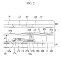
- FIG. 2 is a cross-sectional view of the liquid crystal display of FIG. 1 taken along line II-II'.
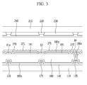
- FIG. 3 is a cross-sectional view of the liquid crystal display of FIG. 1 taken along line III-III'.
- FIG. 4 is a cross-sectional view of the liquid crystal display of FIG. 1 taken along line IV-IV.
- FIG. 5 is a cross-sectional view of the liquid crystal display of FIG. 1 taken along line V-V.
- FIG. 6 is a cross-sectional view of the liquid crystal display of FIG. 1 taken along line VI-VI.
- a liquid crystal display according to an exemplary embodiment of the present disclosure includes a lower panel 100 and an upper panel 200 facing each other, and a liquid crystal layer 3 interposed therebetween.
- a plurality of first and second gate lines 121a and 121b are disposed on a first insulation substrate 110 made of transparent glass or plastic.
- the first gate line 121a and the second gate line 121b are disposed in pairs between pixel rows.
- the first gate line 121a includes a first gate electrode 124a
- the second gate line 121b includes a second gate electrode 124b.
- Each of the gate lines 121a and 121b includes a wide gate pad portion 129 for connection with another layer or an external driving circuit.
- a gate insulating layer 140 is disposed on the plurality of gate lines 121a and 121b.
- a first semiconductor 154a and a second semiconductor 154b are disposed on the gate insulating layer 140.
- the semiconductors 154a and 154b may include an oxide semiconductor.
- Ohmic contacts 163a and 165a are disposed on the semiconductors 154a and 154b. If the semiconductors 154a and 154b include an oxide semiconductor, the ohmic contacts 163a and 165a may be omitted.
- a plurality of data lines 171, a plurality of drain electrodes 175a and 175b, and a plurality of compensation voltage lines 131 are disposed on the ohmic contacts 163a and 165a.
- the data line 171 transmits a data signal and extends in a substantially longitudinal direction thereby intersecting the gate lines 121a and 121b.
- One data line 171 is associated with two columns of pixels.
- the data line 171 may have a first curved portion with a curved shape to maximize transmittance of the liquid crystal display, and the first curved portion may meet a second curved portion which forms a predetermined angle with the first curved portion at a "V" shape in a middle region of the pixel area.
- Each data line 171 includes a first source electrode 173a that extends toward the first gate electrode 124a and a second source electrode 173b that extends toward the second gate electrode 124b.
- Each data line 171 includes a wide data pad portion 179 for connection with another layer or an external driving circuit.
- the first drain electrode 175a includes one end facing the first source electrode 173a and a wide other end, and forms a thin film transistor (TFT) along with the first gate electrode 124a and the first semiconductor 154a.
- TFT thin film transistor
- the second drain electrode 175b includes one end facing the second source electrode 173b and a wide other end, and forms a thin film transistor (TFT) along with the second gate electrode 124b and the second semiconductor 154b.
- TFT thin film transistor
- the compensation voltage line 131 extends parallel to the data line 171, and one compensation voltage line 131 may be associated with two pixel columns.
- the data line 171 and the compensation voltage line 131 may be alternately disposed.
- the compensation voltage line 131 includes a plurality of extensions 135 and includes a wide compensation pad portion 139 for connection with another layer or an external driving circuit.
- a first passivation layer 180x is disposed on the plurality of data lines 171, the plurality of drain electrodes 175a and 175b, and the plurality of compensation voltage lines 131.
- the first passivation layer 180x may be made of an organic insulating material or an inorganic insulating material.
- An organic layer 180 is disposed on the first passivation layer 180x.
- the organic layer 180 may have be thicker than the first passivation layer 180x and may have a flat surface.
- the organic layer 180 may be omitted.
- the organic layer 180 may be a color filter, and in this case, a layer disposed on the organic layer 180 may be further included.
- an overcoat or capping layer may be disposed on the color filter to prevent a color pigment from flowing into the liquid crystal layer, and the overcoat may be made of an insulating material such as a silicon nitride (SiNx).
- the organic layer 180 may be positioned in a display area in which a plurality of pixels are positioned, and may not be positioned in a peripheral area in which the gate pad portion 129, the data pad portion 179, and the compensation pad portion 139 are positioned.
- a first height H1 of the organic layer 180 in the display area is greater than a second height H2 of the organic layer 180 near the gate pad portion 129, the data pad portion 179, and the compensation pad portion 139.
- the organic layer 180 and the first passivation layer 180x are penetrated by a first contact hole 185a that exposes the first drain electrode 175a, a second contact hole 185b that exposes the second drain electrode 175b, and a third contact hole 186a that exposes the extension 135 of the compensation voltage line 131.
- a pixel electrode 191 and a compensation electrode 80 are disposed on the organic layer 180.
- the pixel electrode 191 includes curved edges which are substantially parallel to the first curved portion and the second curved portion of the data line 171.
- the pixel electrode 191 is made of a transparent conductive layer such as ITO or IZO.
- the pixel electrode 191 is positioned at both sides of the data line 171, and is connected to the first drain electrode 175a through the first contact hole 185a and the second drain electrode 175b through the second contact hole 185b.
- the compensation electrode 80 includes a first longitudinal portion 81a, a second longitudinal portion 81b, a first transverse portion 82a, a second transverse portion 82b, and a shielding electrode 83.
- the first longitudinal portion 81a and the second longitudinal portion 81b overlap and extend parallel to the two compensation voltage lines 131 positioned at either side of the data line 171.
- the first transverse portion 82a extends from the first longitudinal portion 81a parallel to the direction of the gate lines 121a and 121b and the second transverse portion 82b extends from the second longitudinal portion 81b parallel to the direction of the gate lines 121a and 121b.
- the shielding electrode 83 is connected to the first transverse portion 82a and the second transverse portion 82b that overlap and are parallel to the data line 171.
- the first longitudinal portion 81a and the second longitudinal portion 81b of the compensation electrode 80 include a plurality of first connections 84 that overlap the extension 135 of the compensation voltage line 131.
- the first connection 84 of the compensation electrode 80 is connected to the compensation voltage line 131 through the third contact hole 186a.
- the pixel electrode 191 and the compensation electrode 80 may be simultaneously formed from the same layer.
- a second passivation layer 180y is disposed on the pixel electrode 191 and the compensation electrode 80.
- the second passivation layer 180y, the first passivation layer 180x, and the gate insulating layer 140 have a fourth contact hole 187 in a region positioned at the gate pad portion 129 where they do not overlap the organic layer 180 that exposes the gate pad portion 129.
- the second passivation layer 180y and the first passivation layer 180x have a fifth contact hole 188 in a region positioned at the data pad portion 179 where they do not overlap the organic layer that exposes the data pad portion 179
- the second passivation layer 180y and the first passivation layer 180x have a sixth contact hole 189a in a region positioned at the compensation pad portion 139 where they do not overlap the organic layer 180 that exposes the compensation pad portion 139.
- a common electrode 270, a first contact assistant 91, a second contact assistant 92, and a third contact assistant 93a are disposed on the second passivation layer 180y.
- the common electrode 270 has a plurality of first cutouts 71 in the pixel area, and a plurality of first branch electrodes 271 defined by the plurality of first cutouts 71.
- the plurality of first branch electrodes 271 overlap the pixel electrode 191.
- the plurality of first branch electrodes 271 extend substantially parallel to the data line 171.
- the first contact assistant 91 is positioned on the gate pad portion 129 exposed through the fourth contact hole
- the second contact assistant 92 is positioned on the data pad portion 179 exposed through the fifth contact hole 188
- the third contact assistant 93a is positioned on the compensation pad portion 139 exposed through the sixth contact hole 189a.
- the common electrode 270, the first contact assistant 91, the second contact assistant 92, and the third contact assistant 93a are formed from a transparent conductive layer such as ITO or IZO.
- a horizontal first alignment layer that is rubbed in a predetermined direction may be disposed on the second passivation layer 180y and the common electrode 270.
- the first alignment layer may include a photoreactive material to be photo-aligned.
- a light blocking member 220 is disposed on a second insulating substrate 210 that is made of transparent glass, plastic, etc.
- the light blocking member 220 is also called a black matrix and prevents light leakage.
- a plurality of color filters 230 are also disposed on the second substrate 210.
- An overcoat 250 is disposed on the color filter 230 and the light blocking member 220.
- the overcoat 250 is made of an organic insulator, prevents exposure of the color filter 230, and provides a flat surface.
- the overcoat 250 may be omitted.
- a horizontal second alignment layer that is rubbed in a predetermined direction may be disposed on the overcoat 250.
- the second alignment layer may include a photoreactive material to be photo-aligned.
- the liquid crystal layer 3 includes a plurality of liquid crystal molecules positioned on the pixel electrode 191 and common electrode 270 that are arranged such that long axis direction thereof is aligned parallel to the display panels 100 and 200.
- the pixel electrode 191 receives a data voltage from the drain electrodes 175a and 175b, and the common electrode 270 receives a common voltage having a predetermined magnitude from a common voltage applying unit disposed outside the display region.
- the pixel electrode 191 and the common electrode 270 are field generating electrodes that generate an electric field that rotates the liquid crystal molecules of the liquid crystal layer 3 in a direction parallel with a direction of the electric field.
- the polarization of light passing through the liquid crystal layer 3 changes according to the rotation direction of the liquid crystal molecules as described above.
- the organic layer 180 is positioned on the first passivation layer 180x of the lower panel 100, and the color filter 230 and the light blocking member 220 are positioned on the upper panel 200.
- the color filter 230 may replace the organic layer 180 on the lower panel 100 and the color filter 230 may be omitted from the upper panel 200.
- the light blocking member 220 may also be positioned on the lower panel 100 instead of the upper panel 200.
- FIG. 7 is a waveform diagram of partial signals applied to a liquid crystal display according to an exemplary embodiment of the present disclosure.
- the data line 171 and the common electrode 270 overlap each other such that a ripple of the common voltage may be generated by a coupling of the voltages applied to the data line 171 and the common electrode 270.
- the compensation electrode 80 which includes the shielding electrode 83 overlapping the data line 171, is applied with a voltage of a polarity opposite to the common voltage ripple, to prevent the ripple from being generated by the coupling between the data line 171 and the common electrode 270.
- the data line 171 and the common electrode 270 overlap each other, thereby forming a first capacitor C1. Accordingly, by the coupling with the data voltage D applied to the data line 171, the common voltage Vcom applied to the common electrode 270 may change by a first magnitude W1. At this time, a compensation voltage Ccps applied to the compensation electrode 80 has the opposite polarity to that of the data voltage D applied to the data line 171.
- the shielding electrode 83 of the compensation electrode 80 which overlaps the data line 171, also overlaps the common electrode 270, thereby forming a second capacitor C2. Accordingly, by the coupling between the shielding electrode 83 and the common electrode 270, the common voltage Vcom applied to the common electrode 270 may change by a second magnitude W2. That is, by applying a voltage having a polarity opposite to the data voltage D to the compensation electrode 80, the first magnitude W1 change of the common voltage Vcom due to the data voltage D is compensated by the coupling due to the compensation voltage Ccps of the compensation electrode 80, thereby maintaining a uniform common voltage magnitude Vcom applied to the common electrode 270.
- FIG. 8 is a layout view of a liquid crystal display according to another exemplary embodiment of the present disclosure.
- the compensation electrode 80 of a liquid crystal display includes the shielding electrode 83 that overlaps some of the plurality of data lines 171.
- the shielding electrode 83 overlaps the data line 171 positioned between the first pixel PXA and the second pixel PXB of four adjacent pixels PXA, PXB, PXC, and PXD, but does not overlap the data line 171 positioned between the third pixel PXC and the fourth pixel PXD.
- FIG. 9 is a layout view of a liquid crystal display according to another exemplary embodiment of the present disclosure.
- FIG. 10 is a cross-sectional view of the liquid crystal display of FIG. 9 taken along line X-X.
- FIG. 11 is a cross-sectional view of the liquid crystal display of FIG. 9 taken along line XI-XI.
- a liquid crystal display according to a present exemplary embodiment includes the lower panel 100 and the upper panel 200 facing each other and the liquid crystal layer 3 interposed therebetween.
- a gate line 121 and a compensation voltage line 131 are disposed on a first insulation substrate 110 made of a transparent glass or plastic.
- the gate line 121 and the compensation voltage line 131 are formed together from the same layer.
- the gate line 121 includes the gate electrode 124 and the gate pad portion 129.
- the compensation voltage line 131 extends parallel to the gate line 121 and includes a plurality of extensions 135 and the compensation pad portion 139.
- a gate insulating layer 140 is disposed on the gate line 121 and the compensation voltage line 131.
- a semiconductor 154 is disposed on the gate insulating layer 140.
- Ohmic contacts 163 and 165 are disposed on the semiconductor 154.
- the ohmic contacts 163 and 165 may be disposed in a pair on the semiconductor 154. If the semiconductor 154 is an oxide semiconductor, the ohmic contacts 163 and 165 may be omitted.
- a data conductor that includes a data line 171, a source electrode 173 and a drain electrode 175 is disposed on the ohmic contacts 163 and 165 and the gate insulating layer 140.
- the data line 171 includes a wide end for connection with other layers or an external driving circuit.
- the data line 171 transmits a data signal and extends in a substantially longitudinal direction thereby intersecting the gate line 121.
- the data line 171 may have a first curved portion with a curved shape to maximize transmittance of the liquid crystal display, and the first curved portion may meet a second curved portion at a center region of the pixel area thereby forming a "V" shape.
- the source electrode 173 is a portion of the data line 171.
- the drain electrode 175 may be disposed parallel to the source electrode 173. Accordingly, the drain electrode 175 is parallel to the portion of the data line 171.
- the gate electrode 124, the source electrode 173, and the drain electrode 175 form a thin film transistor (TFT) along with the semiconductor 154, and a channel of the thin film transistor forms in the semiconductor 154 between the source electrode 173 and the drain electrode 175.
- TFT thin film transistor
- a liquid crystal display includes the source electrode 173 positioned on the same line as the data line 171 and the drain electrode 175 extending parallel to the data line 171 such that the width of the thin film transistor may increase without increasing the area occupied by the data conductor, thereby increasing the aperture ratio of the liquid crystal display.
- the source electrode 173 and the drain electrode 175 have different shapes.
- a first passivation layer 180x is disposed on the data conductor 171, 173, and 175, the gate insulating layer 140, and the portion of the semiconductor 154 exposed between the source electrode 173 and the drain electrode 175.
- the first passivation layer 180x may be made of an organic insulating material or an inorganic insulating material.
- An organic layer 180 is disposed on the first passivation layer 180x.
- the organic layer 180 is thicker than the first passivation layer 180x and may have a flat surface.
- the organic layer 180 may be positioned in the display area where a plurality of pixels are positioned, and may not be positioned in the peripheral area where the gate pad portion and the data pad portion are positioned. Alternatively, the organic layer 180 may be positioned in the peripheral area where the gate pad portion or the data pad portion are positioned, where the organic layer 180 may have a lower surface height than the organic layer 180 positioned at the display area.
- the organic layer 180 and the first passivation layer 180x have a seventh contact hole 185 that exposes the drain electrode 175.
- the organic layer 180, the first passivation layer 180x, and the gate insulating layer 140 have an eighth contact hole 186b that exposes the compensation voltage line 131.
- a pixel electrode 191 and a compensation electrode 80 are disposed on the organic layer 180.
- the compensation electrode 80 overlaps the data line 171 and extends along with the data line 171.
- the compensation electrode 80 includes a second connection 80b that extends toward the extension 135 of the compensation voltage line 131.
- the second connection 80b of the compensation electrode 80 is connected to the compensation voltage line 131 through the eighth contact hole 186b.
- the pixel electrode 191 and the compensation electrode 80 may be simultaneously formed from the same layer.
- a second passivation layer 180y is disposed on the pixel electrode 191 and the compensation electrode 80.
- the second passivation layer 180y, the first passivation layer 180x, and the gate insulating layer 140 have a fourth contact hole 187 in a region positioned at the gate pad portion where they do not overlap the organic layer 180 that exposes the gate pad portion 129.
- the second passivation layer 180y and the first passivation layer 180x have a fifth contact hole 188 in a region positioned at the data pad portion 179 where they do not overlap the organic layer 180 that exposes the data pad portion 179.
- the first passivation layer 180x, the second passivation layer 180y, and the gate insulating layer 140 have a ninth contact hole 189b in a region positioned at the compensation pad portion where they do not overlap the organic layer 180 that exposes the compensation pad portion 139.
- a common electrode 270, a first contact assistant 91, a second contact assistant 92, and a fourth contact assistant 93b are disposed on the second passivation layer 180y.
- the common electrode 270 includes a plurality of first cutouts 71 and a plurality of first branch electrodes 271 defined by the plurality of first cutouts 71.
- a plurality of first branch electrodes 271 overlap the pixel electrode 191.
- a plurality of first branch electrodes 271 extend substantially parallel to the data line 171.
- the first contact assistant 91 is disposed on the gate pad portion 129 exposed through the fourth contact hole 187, and the second contact assistant 92 is disposed on the data pad portion 179 exposed through the fifth contact hole.
- the fourth contact assistant 93b is disposed on the compensation pad portion 139 exposed through the ninth contact hole 189b.
- the common electrode 270, the first contact assistant 91, the second contact assistant 92, and the fourth contact assistant 93b are formed from a transparent conductive layer such as ITO or IZO.
- a light blocking member 220 and a color filter 230 are disposed on the second insulation substrate 210, and an overcoat 250 is disposed on the color filter 230 and the light blocking member 220.
- the compensation electrode 80 overlaps some, but not all data lines 171. However, according to a liquid crystal display of a current exemplary embodiment of the present disclosure, the compensation electrode 80 may overlap all data lines 171.
- the organic layer 180 is positioned on the first passivation layer 180x of the lower panel 100, and the color filter 230 and the light blocking member 220 are positioned on the upper panel 200.
- the color filter 230 may replace the organic layer 180 on the lower panel 100, and the color filter 230 may be omitted from the upper panel 200.
- the light blocking member 220 may also be positioned on the lower panel 100 instead of the upper panel 200.
- a voltage having a polarity opposite to the common voltage ripple is applied to the compensation electrode 80 to prevent the ripple due to the coupling between the data line 171 and the common electrode 270.
- FIG. 12 is a layout view of a liquid crystal display according to another exemplary embodiment of the present disclosure.
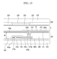
- FIG. 13 is a cross-sectional view of the liquid crystal display of FIG. 12 taken along line XIII-XIII'.
- FIG. 14 is a cross-sectional view of the liquid crystal display of FIG. 12 taken along line XIV-XIV'.
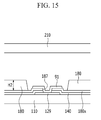
- FIG. 15 is a cross-sectional view of the liquid crystal display of FIG. 12 taken along line XV-XV.
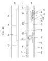
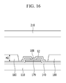
- FIG. 16 is a cross-sectional view of the liquid crystal display of FIG. 12 taken along line XVI-XVI.
- FIG. 17 is a cross-sectional view of the liquid crystal display of FIG. 12 taken along line XVII-XVII.
- a liquid crystal display according to a present exemplary embodiment is similar to the liquid crystal display according to the exemplary embodiment of FIG. 1 to FIG. 6 .
- the description of the same constituent elements is omitted.
- a liquid crystal display according to an exemplary embodiment of the present disclosure includes a lower panel 100 and an upper panel 200 facing each other, and a liquid crystal layer 3 interposed therebetween.
- a plurality of first and second gate lines 121a and 121b are disposed on a first insulation substrate 110.
- the first gate line 121a and the second gate line 121b are disposed in pairs between pixel rows.
- the first gate line 121a includes a first gate electrode 124a
- the second gate line 121b includes a second gate electrode 124b.
- Each of the gate lines 121a and 121b includes a wide gate pad portion 129 for connection with another layer or an external driving circuit.
- a gate insulating layer 140 is disposed on a plurality of gate lines 121a and 121b.
- a first semiconductor 154a and a second semiconductor 154b are disposed on the gate insulating layer 140.
- Ohmic contacts 163a and 165a are disposed on the semiconductors 154a and 154b.
- a plurality of data lines 171, a plurality of drain electrodes 175a and 175b, and a plurality of compensation voltage lines 131 are disposed on the ohmic contacts 163a and 165a.
- the data line 171 transmits a data signal and extends in a substantially longitudinal direction thereby intersecting the gate lines 121a and 121b. Each data line 171 is associated with two columns of pixels.
- Each data line 171 includes a first source electrode 173a that extends toward the first gate electrode 124a and a second source electrode 173b that extends toward the second gate electrode 124b.
- Each data line 171 includes a wide data pad portion 179 for connection with another layer or an external driving circuit.
- the first drain electrode 175a faces the first source electrode 173a and forms a thin film transistor (TFT) along with the first gate electrode 124a and the first semiconductor 154a
- the second drain electrode 175b faces the second source electrode 173b and forms a thin film transistor (TFT) along with the second gate electrode 124b and the second semiconductor 154b.
- the compensation voltage line 131 extends parallel to the data line 171, and each compensation voltage line 131 may associated with two pixel columns.
- the data line 171 and the compensation voltage line 131 may be alternately disposed.
- the compensation voltage line 131 includes a plurality of extensions 135 and a wide compensation pad portion 139 for connection with another layer or an external driving circuit.
- a first passivation layer 180x is disposed on the plurality of data lines 171, the plurality of drain electrodes 175a and 175b, and the plurality of compensation voltage lines 131.
- An organic layer 180 is disposed on the first passivation layer 180x.
- the organic layer 180 may be thicker than the first passivation layer 180x and have a flat surface.
- the organic layer 180 may be positioned in the display area in which a plurality of pixels are positioned, and may not be positioned in a peripheral area in which the gate pad portion 129, the data pad portion 179, and the compensation pad portion 139 are disposed.
- the organic layer 180 and the first passivation layer 180x have a first contact hole 185a that exposes the first drain electrode 175a, a second contact hole 185b that exposes the second drain electrode 175b, and a third contact hole 186a that exposes the extension 135 of the compensation voltage line 131.
- a pixel electrode 191 and a compensation electrode 80 are disposed on the organic layer 180.
- the pixel electrode 191 is positioned on both sides of the data line 171, and is connected to the first drain electrode 175a through the first contact hole 185a and the second drain electrode 175b through the second contact hole 185b.
- the compensation electrode 80 includes a first longitudinal portion 81a, a second longitudinal portion 81b, a first transverse portion 82a, a second transverse portion 82b, and a shielding electrode 83.
- the first longitudinal portion 81a and the second longitudinal portion 81b overlap and extend parallel to two compensation voltage lines 131 positioned at both side of the data line.
- the first transverse portion 82a extends from the first longitudinal portion 81a parallel to the direction of the gate lines 121a and 121b
- the second transverse portion 82b extends from the second longitudinal portion 81b parallel to the direction of the gate lines 121a and 121b.
- the shielding electrode 83 is connected to the first transverse portion 82a and the second transverse portion 82b, and overlaps and is parallel to the data line 171.
- the first longitudinal portion 81a and the second longitudinal portion 81b of the compensation electrode 80 include a plurality of first connections 84 that overlap the extension 135 of the compensation voltage line 131.
- the pixel electrode 191 and the compensation electrode 80 may be simultaneously formed from the same layer.
- the first connection 84 of the compensation electrode 80 is connected to the compensation voltage line 131 through the third contact hole 186a.
- a second passivation layer 180y is disposed on the pixel electrode 191 and the compensation electrode 80.
- the second passivation layer 180y, the first passivation layer 180x, and the gate insulating layer 140 have a fourth contact hole 187 at a region positioned at the gate pad portion 129 where they do not overlap the organic layer 180 that exposes the gate pad portion 129.
- the second passivation layer 180y and the first passivation layer 180x have a fifth contact hole 188 at a region positioned at the data pad portion 179 where they do not overlap the organic layer 180 that exposes the data pad portion 179
- the second passivation layer 180y and the first passivation layer 180x have a sixth contact hole 189a at a region positioned at the compensation pad portion 139 where they do not overlap the organic layer 180 that exposes the compensation pad portion 139.
- a common electrode 270, a first contact assistant 91, a second contact assistant 92, and a third contact assistant 93a are disposed on the second passivation layer 180y.
- the common electrode 270 has a plurality of first cutouts 71 in the pixel area and a plurality of first branch electrodes 271 defined by the plurality of first cutouts 71.
- a plurality of first branch electrodes 271 overlap the pixel electrode 191.
- a plurality of first branch electrodes 271 extend in a direction substantially parallel to the data line 171.
- the common electrode 270 includes a second cutout 274 in a region that overlaps the data line 171.
- the first contact assistant 91 is positioned on the gate pad portion 129 exposed through the fourth contact hole 187
- the second contact assistant 92 is positioned on the data pad portion 179 exposed through the fifth contact hole 188
- the third contact assistant 93a is positioned on the compensation pad portion 139 exposed through the sixth contact hole 189a.
- the common electrode 270 of a liquid crystal display according to a present exemplary embodiment further has a second cutout 274 that overlaps the data line 171.
- the second cutouts 274 in the common electrode 270 may reduce the overlap area between the data line 171 and the common electrode 270. Accordingly, the coupling between the data line 171 and the common electrode 270 may be reduced, which may prevent a common voltage ripple from being generated by the coupling between the data line 171 and the common electrode 270.
- a light blocking member 220 and a color filter 230 are disposed on the second insulation substrate 210, and an overcoat 250 is disposed on the color filter 230 and the light blocking member 220.
- the liquid crystal layer 3 includes a plurality of liquid crystal molecules positioned on the pixel electrode 191 and common electrode 270that are aligned so that long axial directions thereof are parallel to the panels 100 and 200.
- the pixel electrode 191 receives a data voltage from the drain electrode 175, and the common electrode 270 receives a common voltage having a predetermined magnitude from a common voltage application unit disposed outside the display area.
- the pixel electrode 191 and the common electrode 270 are the field generating electrodes that generate an electric field that rotates the liquid crystal molecules of the liquid crystal layer 3 in a direction parallel with a direction of the electric field.
- the polarization of light passing through the liquid crystal layer 3 changes according to the rotation direction of the liquid crystal molecules as described above.
- the organic layer 180 is positioned on the first passivation layer 180x of the lower panel 100, and the color filter 230 and the light blocking member 220 are positioned on the upper panel 200.
- the color filter 230 may replace the organic layer 180 on the lower panel 100, and the color filter 230 may be omitted from the upper panel 200.
- the light blocking member 220 may also be positioned on the lower panel 100 instead of the upper panel 200.
- a voltage having a polarity opposite to the ripple voltage is applied to the compensation electrode 80 to prevent the ripple due to the coupling between the data line 171 and the common electrode 270.
- the second cutouts 274 in the common electrode 270 may reduce the overlap area between the data line 171 and the common electrode 270. Accordingly, by reducing the coupling between the data line 171 and the common electrode 270, the common voltage ripple generated by the coupling between the data line 171 and the common electrode 270 may be further prevented.
- FIG. 18 is a layout view of a liquid crystal display according to another exemplary embodiment of the present disclosure.
- FIG. 19 is a cross-sectional view of the liquid crystal display of FIG. 18 taken along line XIX-XIX'.
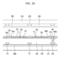
- FIG. 20 is a cross-sectional view of the liquid crystal display of FIG. 18 taken along line XX-XX'.
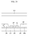
- FIG. 21 is a cross-sectional view of the liquid crystal display of FIG. 18 taken along line XXI-XXI.
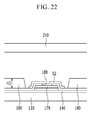
- FIG. 22 is a cross-sectional view of the liquid crystal display of FIG. 18 taken along line XXII-XXII.
- FIG. 23 is a cross-sectional view of the liquid crystal display of FIG. 18 taken along line XXIII-XXIII.
- a liquid crystal display according to a present exemplary embodiment is similar to the liquid crystal display according to the exemplary embodiment of FIG. 1 to FIG. 6 .
- the description of the same constituent elements is omitted.
- a liquid crystal display according to an exemplary embodiment of the present disclosure includes a lower panel 100 and an upper panel 200 facing each other, and a liquid crystal layer 3 interposed therebetween.
- a plurality of first and second gate lines 121a and 121b are disposed on a first insulation substrate 110.
- the first gate line 121a and the second gate line 121b are disposed in pairs between pixel rows.
- the first gate line 121a includes a first gate electrode 124a
- the second gate line 121b includes a second gate electrode 124b.
- Each of the gate lines 121a and 121b includes a wide gate pad portion 129 for connection with another layer or an external driving circuit.
- a gate insulating layer 140 is disposed on the plurality of gate lines 121a and 121b.
- a first semiconductor 154a and a second semiconductor 154b are disposed on the gate insulating layer 140.
- Ohmic contacts 163a and 165a are disposed on the semiconductors 154a and 154b.
- a plurality of data lines 171, a plurality of drain electrodes 175a and 175b, and a plurality of compensation voltage lines 131 are disposed on the ohmic contacts 163a and 165a.
- the data line 171 transmits a data signal and extends in a substantially longitudinal direction thereby intersecting the gate lines 121a and 121b. Each data line 171 is associated with two columns of pixels.
- Each data line 171 includes a first source electrode 173a that extends toward the first gate electrode 124a and a second source electrode 173b that extends toward the second gate electrode 124b.
- Each data line 171 includes a wide data pad portion 179 for connection with another layer or an external driving circuit.
- the first drain electrode 175a faces the first source electrode 173a and forms a thin film transistor (TFT) along with the first gate electrode 124a and the first semiconductor 154a
- the second drain electrode 175b faces the second source electrode 173b and forms a thin film transistor (TFT) along with the second gate electrode 124b and the second semiconductor 154b.
- the compensation voltage line 131 extends parallel to the data line 171 and each may be associated with two pixel columns.
- the data line 171 and the compensation voltage line 131 may be alternately disposed.
- the compensation voltage line 131 includes a plurality of extensions 135 and a wide compensation pad portion 139 for connection with another layer or an external driving circuit.
- a first passivation layer 180x is disposed on the plurality of data lines 171, the plurality of drain electrodes 175a and 175b, and the plurality of compensation voltage lines 131.
- An organic layer 180 is disposed on the first passivation layer 180x.
- the organic layer 180 may be thicker than the first passivation layer 180x and have a flat surface.
- the organic layer 180 may be positioned in the display area in which a plurality of pixels are positioned and may not be positioned in a peripheral area in which the gate pad portion 129, the data pad portion 179, and the compensation pad portion 139 are positioned.
- a first height H1 of the organic layer 180 positioned at the display area may be greater than a second height H2 of the organic layer 180 positioned near the gate pad portion 129, the data pad portion 179, and the compensation pad portion 139.
- the organic layer 180 and the first passivation layer 180x have a first contact hole 185a that exposes the first drain electrode 175a, a second contact hole 185b that exposes the second drain electrode 175b, and a third contact hole 186a that exposes the extension 135 of the compensation voltage line 131.
- the second passivation layer 180y and the first passivation layer 180x have a fourth contact hole 187 at a region positioned at the gate pad portion 129 where they do not overlap the organic layer 180 that exposes the gate pad portion 129.
- the first passivation layer 180x has a fifth contact hole 188 at a region positioned at the data pad portion 179 where it does not overlap the organic layer 180 that exposes the data pad portion 179
- the first passivation layer 180x has a sixth contact hole 189a at a region positioned at the compensation pad portion 139 where it does not overlap the organic layer 180 that exposes the compensation pad portion 139.
- a pixel electrode 191 and a compensation electrode 80 are disposed on the organic layer 180.
- the pixel electrode 191 includes a curved edge that is substantially parallel to a first curved portion of the data line 171.
- the pixel electrode 191 is formed from a transparent conductive layer such as ITO or IZO.
- the pixel electrode 191 is positioned on both sides of the data line 171, and is connected to the first drain electrode 175a through the first contact hole 185a and the second drain electrode 175b through the second contact hole 185b.
- the compensation electrode 80 includes a first longitudinal portion 81a, a second longitudinal portion 81b, a first transverse portion 82a, a second transverse portion 82b and a shielding electrode 83.
- the first longitudinal portion 81a and second longitudinal portion 81b overlap and extend parallel to two compensation voltage lines 131 positioned at both sides of the data line.
- the first transverse portion 82a extends from the first longitudinal portion 81a parallel to the direction of the gate lines 121a and 121b
- the second transverse portion 82b extends from the second longitudinal portion 81b parallel to the direction of the gate lines 121a and 121b.
- the shielding electrode 83 is connected to the first transverse portion 82a and the second transverse portion 82b, and overlaps and is parallel to the data line 171.
- the pixel electrode 191 and the compensation electrode 80 may be simultaneously formed from the same layer.
- the first longitudinal portion 81a and the second longitudinal portion 81b of the compensation electrode 80 include a plurality of first connections 84 that overlap the extension 135 of the compensation voltage line 131.
- the first connection 84 of the compensation electrode 80 is connected to the compensation voltage line 131 through the third contact hole 186a.
- a second passivation layer 180y is disposed on the pixel electrode 191 and the compensation electrode 80, and a common electrode 270, a first contact assistant 91, a second contact assistant 92, and a third contact assistant 93a are disposed on the second passivation layer 180y.
- the common electrode 270 is formed from a transparent conductive layer such as ITO or IZO.
- the first contact assistant 91 is positioned on the gate pad portion 129 exposed through the fourth contact hole 187
- the second contact assistant 92 is positioned on the data pad portion 179 exposed through the fifth contact hole 188
- the third contact assistant 93a is positioned on the compensation pad portion 139 exposed through the sixth contact hole 189a.
- the second passivation layer 180y and the common electrode 270 have substantially the same planar shape.
- the second passivation layer 180y and the common electrode 270 are positioned in the display area where a plurality of pixels are positioned, but are not positioned at the peripheral area where the gate pad portion 129 and the data pad portion 179 are positioned.
- the common electrode 270 has a plurality of first cutouts 71, and the second passivation layer 180y has a plurality of third cutouts 181.
- the first cutouts 71 and the third cutouts 181 have substantially the same planar shape. That is, an edge of the first cutout 71 and an edge of the third cutout 181 overlap each other. Therefore, the second passivation layer 180y and the common electrode 270 may be formed together using one photomask.
- the common electrode 270 includes a sixth cutout 38a and a seventh cutout 38b near the first drain electrode 175a and the second drain electrode 175b.
- a horizontal first alignment layer rubbed in a predetermined direction may be applied on the pixel electrode 191 and the common electrode 270 exposed through the third cutout .
- the first alignment layer may include a photoreactive material to be photo-aligned.
- a light blocking member 220 is disposed on a second insulating substrate 210 made of transparent glass, plastic, etc.
- a plurality of color filters 230 are also disposed on the second substrate 210.
- An overcoat 250 is disposed on the color filter 230 and the light blocking member 220.
- a second alignment layer may be disposed on the overcoat 250.
- the liquid crystal layer 3 includes a plurality of liquid crystal molecules positioned on the pixel electrode 191 and common electrode 270that are arranged such that long axis direction thereof is aligned parallel to the display panels 100 and 200.
- the pixel electrode 191 receives a data voltage from the drain electrodes 175a and 175b and the common electrode 270 receives a common voltage having a predetermined magnitude from a common voltage applying unit which is disposed outside the display region.
- the pixel electrode 191 and the common electrode 270 are field generating electrodes that generate an electric field that rotate the liquid crystal molecules of the liquid crystal layer 3 in a direction parallel with a direction of the electric field.
- the polarization of light passing through the liquid crystal layer 3 changes according to the rotation direction of the liquid crystal molecules as described above.
- the organic layer 180 is positioned on the first passivation layer 180x of the lower panel 100, and the color filter 230 and the light blocking member 220 are positioned on the upper panel 200.
- the color filter 230 may replace the organic layer 180 on the lower panel 100 and the color filter 230 may be omitted from the upper panel 200.
- the light blocking member 220 may also be positioned on the lower panel 100 instead of the upper panel 200.
- the common electrode 270 has a plurality of first cutouts 71
- the second passivation layer 180y has a plurality of third cutouts 181
- the first cutouts 71 and the third cutouts 181 have substantially the same planar shape. That is, an edge of the first cutout 71 and an edge of the third cutout 181 180y overlap. Therefore, the second passivation layer 180y and the common electrode 270 may be formed together with one photomask.
- the second passivation layer 180y and the common electrode 270 are positioned in the display area where a plurality of pixels are positioned, but are not positioned in the peripheral area where the gate pad portion 129 and the data pad portion 179 are positioned.
- the compensation electrode 80 of a liquid crystal display includes a shielding electrode 83 that overlaps the data line 171, and to compensate the ripple of the common voltage, a voltage having a polarity opposite to the common voltage ripple is applied to the compensation electrode 80, thereby preventing the ripple due to the coupling between the data line 171 and the common electrode 270.
- the shielding electrode 83 of the compensation electrode 80 overlaps some, but not all of the plurality of data lines 171.
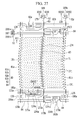
- FIG. 24 is a layout view of a liquid crystal display according to another exemplary embodiment of the present disclosure.
- FIG. 25 is a cross-sectional view of the liquid crystal display of FIG. 24 taken along line XXV-XXV.
- FIG. 26 is a cross-sectional view of the liquid crystal display of FIG. 24 taken along line XXVI-XXVI.
- the liquid crystal display according to the present exemplary embodiment includes a lower panel 100 and an upper panel 200 facing each other, and a liquid crystal layer 3 interposed therebetween.
- a gate line 121 and a compensation voltage line 131 are disposed on a first insulation substrate 110 made of transparent glass or plastic.
- the gate line 121 and the compensation voltage line 131 are formed together from a same layer.
- the gate line 121 includes agate electrode 124 and a gate pad portion 129.
- the compensation voltage line 131 extends parallel to the gate line 121 and includes a plurality of extensions 135 and a compensation pad portion 139.
- a gate insulating layer 140 is disposed on the gate line 121 and the compensation voltage line 131.
- a semiconductor 154 is disposed on the gate insulating layer 140.
- Ohmic contacts 163 and 165 are disposed on the semiconductor 154.
- a data conductor that includes a data line 171, a source electrode 173 and a drain electrode 175 is disposed on the ohmic contacts 163 and 165 and the gate insulating layer 140.
- the source electrode 173 is a portion of the data line 171, and is positioned on the same line as the data line 171.
- the drain electrode 175 may be disposed parallel to the source electrode 173. Accordingly, the drain electrode 175 is parallel to a portion of the data line 171.
- a first passivation layer 180x is disposed on the data conductors 171, 173, and 175, the gate insulating layer 140, and the exposed portion of the semiconductor 154.
- An organic layer 180 is disposed on the first passivation layer 180x.
- the organic layer 180 is thicker than the first passivation layer 180x and may have a flat surface.
- the organic layer 180 may be positioned in the display area where a plurality of pixels are positioned, and may not be positioned in the peripheral area where the gate pad portion and the data pad portion are positioned. Alternatively, the organic layer 180 may be positioned in the peripheral area where the gate pad portion and the data pad portion are positioned, where the organic layer 180 may have a lower surface height than the organic layer 180 positioned at the display area.
- the organic layer 180 and the first passivation layer 180x have a seventh contact hole 185 that exposes the drain electrode 175.
- the organic layer 180, the first passivation layer 180x, and the gate insulating layer 140 have an eighth contact hole 186b that exposes the compensation voltage line 131.
- the first passivation layer 180x and the gate insulating layer 140 have a fourth contact hole 187 at a region positioned at the gate pad portion 129 where they do not overlap the organic layer 180 that exposes the gate pad portion 129.
- the first passivation layer 180x has a fifth contact hole 188 at a region positioned at the data pad portion 179 where it does not overlap the organic layer 180 that exposes the data pad portion 179.
- the first passivation layer 180x and the gate insulating layer 140 have a ninth contact hole 189b at a region positioned at the compensation pad portion 139 where they do not overlap the organic layer 180 that exposes the compensation pad portion 139.
- a pixel electrode 191 and a compensation electrode 80 are disposed on the organic layer 180.
- the compensation electrode 80 overlaps the data line 171 and extends along with the data line 171.
- the compensation electrode 80 includes a second connection 80b that extends toward the extension 135 of the compensation voltage line 131.
- the second connection 80b of the compensation electrode 80 is connected to the compensation voltage line 131 through the eighth contact hole 186b.
- the pixel electrode 191 and the compensation electrode 80 may be simultaneously formed from a same layer.
- a second passivation layer 180y is disposed on the pixel electrode 191 and the compensation electrode 80, and a common electrode 270, a first contact assistant 91, a second contact assistant 92, and a fourth contact assistant 93b are disposed on the second passivation layer 180y.
- the common electrode 270 is formed from a transparent conductive layer such as ITO or IZO.
- the first contact assistant 91 is positioned on the gate pad portion 129 exposed through the fourth contact hole 187
- the second contact assistant 92 is positioned on the data pad portion 179 exposed through the fifth contact hole
- the fourth contact assistant 93b is positioned on the compensation pad portion 139 exposed through the nine contact hole 189b.
- the second passivation layer 180y and the common electrode 270 positioned on the second passivation layer 180y have substantially the same planar shape.
- the second passivation layer 180y and the common electrode 270 are positioned in the display area where a plurality of pixels are positioned, but are not positioned at the peripheral area where the gate pad portion 129 and the data pad portion 179 are positioned.
- the common electrode 270 has a plurality of first cutouts 71
- the second passivation layer 180y has a plurality of third cutouts 181.
- the first cutout 71 of the common electrode 270 and the third cutout 181 of the second passivation layer 180y have substantially the same planar shape. That is, an edge of the first cutout 71 and an edge of the third cutout 181 overlap each other. Therefore, the second passivation layer 180y and the common electrode 270 may be formed together using one photomask.
- a light blocking member 220 and a color filter 230 are disposed on the second insulation substrate 210, and an overcoat 250 is disposed on the color filter 230 and the light blocking member 220.
- the compensation electrode 80 overlaps some, but not all data lines 171. However, according to a liquid crystal display of another exemplary embodiment of the present disclosure, the compensation electrode 80 may overlap all data lines 171.
- the organic layer 180 is positioned on the first passivation layer 180x of the lower panel 100, and the color filter 230 and the light blocking member 220 are positioned on the upper panel 200.
- the color filter 230 may replace the organic layer 180 on the lower panel 100 and the color filter 230 may be omitted from the upper panel 200.
- the light blocking member 220 may also be positioned on the lower panel 100 instead of the upper panel 200.
- the common electrode 270 has a plurality of first cutouts 71
- the second passivation layer 180y has a plurality of third cutouts 181
- the first cutouts 71 and the third cutouts 181 have substantially the same planar shape. That is, the edge of the first cutouts 71 and the edge of the third cutouts 181overlap. Therefore, the second passivation layer 180y and the common electrode 270 may be formed together with one photomask.
- the second passivation layer 180y and the common electrode 270 are positioned in the display area where a plurality of pixels are positioned, but are not positioned at the peripheral area where the gate pad portion 129 and the data pad portion 179 are positioned.
- a voltage having an opposite polarity to the ripple voltage is applied to the compensation electrode 80, to prevent the ripple due to the coupling between the data line 171 and the common electrode 270.
- FIG. 27 is a layout view of a liquid crystal display according to another exemplary embodiment of the present disclosure.
- FIG. 28 is a cross-sectional view of the liquid crystal display of FIG. 27 taken along the line XXVIII-XXVIII.
- FIG. 29 is a cross-sectional view of the liquid crystal display of FIG. 27 taken along the line XXIX-XXIX.
- FIG. 30 is a cross-sectional view of the liquid crystal display of FIG. 27 taken along the line XXX-XXX.
- FIG. 31 is a cross-sectional view of the liquid crystal display of FIG. 27 taken along the line XXXI-XXXI.
- FIG. 32 is a cross-sectional view of the liquid crystal display of FIG. 27 taken along the line XXXII-XXXII.
- a liquid crystal display according to a present exemplary embodiment is similar to a liquid crystal display according to an exemplary embodiment of FIG. 18 to FIG. 23 .
- the description of the same constituent elements is omitted.
- a liquid crystal display according to an exemplary embodiment of the present disclosure includes a lower panel 100 and an upper panel 200 facing each other, and a liquid crystal layer 3 interposed therebetween.
- a plurality of first and second gate lines 121a and 121b are disposed on a first insulation substrate 110.
- the first gate line 121a and the second gate line 121b are disposed in pairs between pixel rows.
- the first gate line 121a includes a first gate electrode 124a
- the second gate line 121b includes a second gate electrode 124b.
- Each of the gate lines 121a and 121b includes a wide gate pad portion 129 for connection with another layer or an external driving circuit.
- a gate insulating layer 140 is disposed on the plurality of gate lines 121a and 121b.
- a first semiconductor 154a and a second semiconductor 154b are disposed on the gate insulating layer 140.
- Ohmic contacts 163a and 165a are disposed on the semiconductors 154a and 154b.
- a plurality of data lines 171, a plurality of drain electrodes 175a and 175b, and a plurality of compensation voltage lines 131 are disposed on the ohmic contacts 163a and 165a.
- the data line 171 transmits a data signal and extends in a substantially longitudinal direction thereby intersecting the gate lines 121a and 121b. Each data line 171 is associated with two columns of the pixels.
- Each data line 171 includes a first source electrode 173a that extends toward the first gate electrode 124a and a second source electrode 173b that extends toward the second gate electrode 124b.
- Each data line 171 includes a wide data pad portion 179 for connection with another layer or an external driving circuit.
- the first drain electrode 175a faces the first source electrode 173a and forms a thin film transistor (TFT) along with the first gate electrode 124a and the first semiconductor 154a" and the second drain electrode 175b faces the second source electrode 173b and forms a thin film transistor (TFT) along with the second gate electrode 124b and the second semiconductor 154b.
- TFT thin film transistor
- the compensation voltage line 131 extends parallel to the data line 171 and each may be associated with two pixel columns.
- the data line 171 and the compensation voltage line 131 may be alternately disposed.
- the compensation voltage line 131 includes a plurality of extensions 135 and a wide compensation pad portion 139 for connection with another layer or an external driving circuit.
- a first passivation layer 180x is disposed on a plurality of data lines 171, a plurality of drain electrode 175a and 175b, and a plurality of compensation voltage line 131.
- An organic layer 180 is disposed on the first passivation layer 180x.
- the organic layer 180 may be thicker than the first passivation layer 180x and have a flat surface.
- the organic layer 180 may be positioned in the display area in which a plurality of pixels are positioned, and may not be positioned in a peripheral area in which the gate pad portion 129, the data pad portion 179, and the compensation pad portion 139 are positioned.
- the organic layer 180 and the first passivation layer 180x have a first contact hole 185a that exposes the first drain electrode 175a, a second contact hole 185b that exposes the second drain electrode 175b, and a third contact hole 186a that exposes the extension 135 of the compensation voltage line 131.
- the first passivation layer 180x and the gate insulating layer 140 have a fourth contact hole 187 at a region positioned at the gate pad portion 129 where they do not overlap the organic layer 180 that exposes the gate pad portion 129.
- the first passivation layer 180x has a fifth contact hole 188 at a region positioned at the data pad portion 179 where it does not overlap the organic layer 180 that exposes the data pad portion 179
- the first passivation layer 180x has a sixth contact hole 189a at a region positioned at the compensation pad portion 139 where it does not overlap the organic layer 180 that exposes the compensation pad portion 139.
- a pixel electrode 191 and a compensation electrode 80 are disposed on the organic layer 180.
- the pixel electrode 191 is positioned at both sides of the data line 171, and is connected to the first drain electrode 175a through the first contact hole 185a and the second drain electrode 175b through the second contact hole 185b.
- the compensation electrode 80 includes a first longitudinal portion 81a, a second longitudinal portion 81b, a first transverse portion 82a, a second transverse portion 82b, and a shielding electrode 83.
- the first longitudinal portion 81a and the second longitudinal portion 81b overlap and extend parallel to two compensation voltage lines 131 positioned at both sides of the data line 171.
- the first transverse portion 82a extends from the first longitudinal portion 81a parallel to the direction of the gate lines 121a and 121b
- the second transverse portion 82b extends from the second longitudinal portion 81b parallel to the direction of the gate lines 121a and 121b.
- the shielding electrode 83 is connected to the first transverse portion 82a and the second transverse portion 82b, and overlaps and is parallel to the data line 171.
- the first longitudinal portion 81a and the second longitudinal portion 81b of the compensation electrode 80 include a plurality of first connections 84 that overlap the extension 135 of the compensation voltage line 131.
- the first connection 84 of the compensation electrode 80 is connected to the compensation voltage line 131 through the third contact hole 186a.
- the pixel electrode 191 and the compensation electrode 80 may be simultaneously formed from the same layer.
- a second passivation layer 180y is disposed on the pixel electrode 191 and the compensation electrode 80, and a common electrode 270, a first contact assistant 91, a second contact assistant 92, and a third contact assistant 93a are disposed on the second passivation layer 180y.
- the first contact assistant 91 is positioned on the gate pad portion 129 exposed through the fourth contact hole 187
- the second contact assistant 92 is positioned on the data pad portion 179 exposed through the fifth contact hole 188
- the third contact assistant 93a is positioned on the compensation pad portion 139 exposed through the sixth contact hole 189a.
- the second passivation layer 180y and the common electrode 270 positioned on the second passivation layer 180y have substantially the same planar shape.
- the second passivation layer 180y and the common electrode 270 are positioned in the display area where a plurality of pixels are positioned, but are not positioned in the peripheral area where the gate pad portion 129 and the data pad portion 179 are positioned.
- the common electrode 270 has a plurality of first cutouts 71, and the second passivation layer 180y has a plurality of third cutouts 181.
- the common electrode 270 of a liquid crystal display according to a present exemplary embodiment further includes a second cutout 274 at a region overlapping the data line 171, and the second passivation layer 180y further includes a fourth cutout 184 at a region overlapping the data line 171.
- the first cutout 71 of the common electrode 270 and the third cutout 181 of the second passivation layer 180y have substantially the same planar shape
- the second cutout 274 of the common electrode 270 and the fourth cutout 184 of the second passivation layer 180y have substantially the same planar shape.
- An edge of the first cutout 71 overlaps an edge of the third cutout 181
- an edge of the second cutout 274 overlaps an edge of the fourth cutout 184. Therefore, the second passivation layer 180y and the common electrode 270 may be formed together using one photomask.
- a light blocking member 220 and a color filter 230 are disposed on the second insulation substrate 210, and an overcoat 250 is disposed on the color filter 230 and the light blocking member 220.
- the liquid crystal layer 3 includes a plurality of liquid crystal molecules positioned on the pixel electrode 191 and the common electrode 270, and are arranged such that long axis direction thereof is aligned parallel to the display panels 100 and 200.
- the pixel electrode 191 receives a data voltage from the drain electrodes 175a and 175b, and the common electrode 270 receives a common voltage having a predetermined magnitude from a common voltage applying unit which is disposed outside the display region.
- the pixel electrode 191 and the common electrode 270 are the field generating electrodes that generate an electric field that rotates the liquid crystal molecules of the liquid crystal layer 3 in a direction parallel with a direction of the electric field.
- the polarization of light passing through the liquid crystal layer 3 changes due to the rotation direction of the liquid crystal molecules as described above.
- the organic layer 180 is positioned on the first passivation layer 180x of the lower panel 100, and the color filter 230 and the light blocking member 220 are positioned on the upper panel 200.
- the color filter 230 may replace the organic layer 180 on the lower panel 100 and the color filter 230 may be omitted from the upper panel 200.
- the light blocking member 220 may also be positioned on the lower panel 100 instead of the upper panel 200.
- the voltage having a polarity opposite to the ripple voltage is applied to the compensation electrode 80 to prevent the ripple due to the coupling between the data line 171 and the common electrode 270.
- the common electrode 270 has a second cutout 274 in the region overlapping the data line 171, which may reduce the overlap area between the data line 171 and the common electrode 270. Accordingly, reducing the coupling between the data line 171 and the common electrode 270 may further prevent a common voltage ripple generated by the coupling between the data line 171 and the common electrode 270.
- FIG. 33 is a layout view of a liquid crystal display according to another exemplary embodiment of the present disclosure.
- FIG. 34 is a cross-sectional view of the liquid crystal display of FIG. 33 taken along the line XXXIV-XXXIV'.
- FIG. 35 is a cross-sectional view of the liquid crystal display of FIG. 33 taken along the line XXXV-XXXV'.
- a liquid crystal display according to an exemplary embodiment of the present disclosure includes a lower panel 100 and an upper panel 200 facing each other, and a liquid crystal layer 3 interposed therebetween.
- a plurality of first and second gate lines 121a and 121b are disposed on a first insulation substrate 110 made of a transparent glass or plastic.
- the first gate line 121a and the second gate line 121b are disposed in pairs between pixel rows.
- the first gate line 121a includes a first gate electrode 124a
- the second gate line 121b includes a second gate electrode 124b.
- Each of the gate lines 121a and 121b includes a wide gate pad portion 129 for connection with another layer or an external driving circuit.
- a gate insulating layer 140 is disposed on the plurality of gate lines 121a and 121b.
- a first semiconductor 154a and a second semiconductor 154b are disposed on the gate insulating layer 140.
- the semiconductors 154a and 154b may include an oxide semiconductor.
- Ohmic contacts 163a and 165a are disposed on the semiconductors 154a and 154b. If the semiconductors 154a and 154b include an oxide semiconductor, the ohmic contacts 163a and 165a may be omitted.
- a plurality of data lines 171, a plurality of drain electrodes 175a and 175b, and a plurality of compensation voltage lines 131 are disposed on the ohmic contacts 163a and 165a.
- the data line 171 transmits a data signal and extends in a substantially longitudinal direction thereby intersecting the gate lines 121a and 121b. Each data line 171 is associated with two columns of pixels.
- the data line 171 may have a first curved portion with a curved shape to acquire maximize transmittance of the liquid crystal display, and the first curved portion may meet a second curved portion which forms a predetermined angle with the first curved portion at a "V" shape in a middle region of the pixel area.
- Each data line 171 includes a first source electrode 173a that extends toward the first gate electrode 124a and a second source electrode 173b that extends toward the second gate electrode 124b.
- Each data line 171 includes a wide data pad portion 179 for connection with another layer or an external driving circuit.
- the first drain electrode 175a includes one end that faces the first source electrode 173a and a wide other end, and forms a thin film transistor (TFT) along with the first gate electrode 124a and the first semiconductor 154a.
- TFT thin film transistor
- the second drain electrode 175b includes one end that faces the second source electrode 173b and a wide other end, and forms a thin film transistor (TFT) along with the second gate electrode 124b and the second semiconductor 154b.
- TFT thin film transistor
- the compensation voltage line 131 extends parallel to the data line 171 and each may be associated with two pixel columns.
- the data line 171 and the compensation voltage line 131 may be alternately disposed.
- the compensation voltage line 131 includes a plurality of extensions 135, and includes a wide compensation pad portion 139 for connection with another layer or an external driving circuit.
- a first passivation layer 180x is disposed on the plurality of data lines 171, the plurality of drain electrodes 175a and 175b, and the plurality of compensation voltage lines 131.
- the first passivation layer 180x may be made of an organic insulating material or an inorganic insulating material.
- An organic layer 180 is disposed on the first passivation layer 180x.
- the organic layer 180 may be thicker than the first passivation layer 180x, and have a flat surface.
- the organic layer 180 may be omitted.
- the organic layer 180 may be a color filter, and in this case, a layer disposed on the organic layer 180 may be further included.
- an overcoat or capping layer may be disposed on the color filter to prevent a color filter pigment from flowing into the liquid crystal layer, and the overcoat may be made of an insulating material such as a silicon nitride (SiNx).
- the organic layer 180 may be positioned in the display area in which a plurality of pixels are positioned, and may not be positioned in a peripheral area in which the gate pad portion 129, the data pad portion 179, and the compensation pad portion 139 are positioned.
- a first height H1 of the organic layer 180 positioned in the display area is greater than a second height H2 of the organic layer 180 positioned near the gate pad portion 129, the data pad portion 179, and the compensation pad portion 139.
- a common electrode 270 is disposed on the organic layer 180.
- the common electrode 270 is disposed on the whole display area and may have a plate-type planar shape, and is connected to a common electrode 270 disposed in an adjacent pixel.
- a plate type means a planar shape without splitting.
- the common electrode 270 includes a sixth cutout 38a at a region that overlaps the first drain electrode 175a, a seventh cutout 38b at a region that overlaps the second drain electrode 175b, and an eighth cutout 38c at a region that overlaps the extension 135 of the compensation voltage line 131.
- a second passivation layer 180y is disposed on the common electrode 270.
- the second passivation layer 180y, the organic layer 180, and the first passivation layer 180x have a first contact hole 185a that exposes the first drain electrode 175a, a second contact hole 185b that exposes the second drain electrode 175b, and a third contact hole 186a that exposes the extension 135 of the compensation voltage line 131.
- the first contact hole 185a is disposed in the sixth cutout 38a of the common electrode 270
- the second contact hole 185b is disposed in the seventh cutout 38b of the common electrode 270
- the third contact hole 186a is disposed in the eighth cutout 38c of the common electrode 270.
- the second passivation layer 180y, the first passivation layer 180x, and the gate insulating layer 140 have a fourth contact hole 187 in a region positioned at the gate pad portion 129 where they do not overlap the organic layer 180 that exposes the gate pad portion 129.
- the second passivation layer 180y and the first passivation layer 180x have a fifth contact hole 188 in a region positioned at the data pad portion where they do not overlap the organic layer that exposes the data pad portion 179
- the second passivation layer 180y and the first passivation layer 180x have a sixth contact hole 189a in a region positioned at the compensation pad portion 139 where they do not overlap the organic layer 180 that exposes the compensation pad portion 139.
- a pixel electrode 191, a compensation electrode 80, a first contact assistant 91, a second contact assistant 92, and a third contact assistant 93a are disposed on the second passivation layer 180y.
- the pixel electrode 191 has a plurality of fifth cutouts 193.
- the pixel electrode 191 includes a plurality of second branch electrodes 192 defined by the plurality of fifth cutouts 193.
- a plurality of second branch electrodes 192 of the pixel electrode 191 extend substantially parallel to the data line 171 and overlap the common electrode 270.
- the pixel electrode 191 is positioned at both sides of the data line 171, and is connected to the first drain electrode 175a through the first contact hole 185a and the second drain electrode 175b through the second contact hole 185b.
- the compensation electrode 80 includes a first longitudinal portion 81a, a second longitudinal portion 81b, a first transverse portion 82a, a second transverse portion 82b, and a shielding electrode 83.
- the first longitudinal portion 81a and the second longitudinal portion 81b extend parallel to and overlap two compensation voltage lines 131 positioned at both sides of the data line 171.
- the first transverse portion 82a extends from the first longitudinal portion 81a parallel to the direction of the gate lines 121a and 121b
- the second transverse portion 82b extends from the second longitudinal portion 81b parallel to the direction of the gate lines 121a and 121b.
- the shielding electrode 83 is connected to the first transverse portion 82a and the second transverse portion 82b and is parallel to and overlaps the data line 171.
- the first longitudinal portion 81a and the second longitudinal portion 81b of the compensation electrode 80 include a plurality of first connections 84 that overlap the extension 135 of the compensation voltage line 131.
- the first connection 84 of the compensation electrode 80 is connected to the compensation voltage line 131 through the third contact hole 186a.
- the first contact assistant 91 is positioned on the gate pad portion 129 exposed through the fourth contact hole 187
- the second contact assistant 92 is positioned on the data pad portion 179 exposed through the fifth contact hole 188
- the third contact assistant 93a is positioned on the compensation pad portion 139 exposed through the sixth contact hole 189a.
- the pixel electrode 191, the compensation electrode 80, the first contact assistant 91, the second contact assistant 92, and the third contact assistant 93a are formed from a transparent conductive layer such as ITO or IZO.
- the pixel electrode 191, the compensation electrode 80, the first contact assistant 91, the second contact assistant 92, and the third contact assistant 93a may be simultaneously formed from a same layer.
- a horizontal first alignment layer rubbed in a predetermined direction may be applied on the second passivation layer 180y and the pixel electrode 191.
- the first alignment layer may include a photoreactive material to be photo-aligned.
- a light blocking member 220 is disposed on a second insulating substrate 210 made of transparent glass, plastic, etc.
- the light blocking member 220 is also called a black matrix and prevents light leakage.
- a plurality of color filters 230 are also disposed on the second substrate 210.
- An overcoat 250 is disposed on the color filter 230 and the light blocking member 220.
- the overcoat 250 is made of an organic insulator, prevents exposure of the color filter 230, and provides a flat surface.
- the overcoat 250 may be omitted.
- a horizontal second alignment layer rubbed in a predetermined direction may be disposed on the overcoat 250.
- the second alignment layer may include a photoreactive material to be photo-aligned.
- the liquid crystal layer 3 includes a plurality of liquid crystal molecules positioned on the pixel electrode 191 and the common electrode 270 that are arranged such that long axis direction thereof is aligned parallel to the display panels 100 and 200.
- the pixel electrode 191 receives a data voltage from the drain electrodes 175a and 175b and the common electrode 270 receives a common voltage having a predetermined magnitude from a common voltage applying unit which is disposed outside the display region.
- the pixel electrode 191 and the common electrode 270 are field generating electrodes that generate an electric field that rotates the liquid crystal molecules of the liquid crystal layer 3 in a direction parallel with a direction of the electric field.
- the polarization of light passing through the liquid crystal layer 3 changes due to the rotation direction of the liquid crystal molecules as described above.
- the organic layer 180 is positioned on the first passivation layer 180x of the lower panel 100, and the color filter 230 and the light blocking member 220 are positioned on the upper panel 200.
- the color filter 230 may replace the organic layer 180 on the lower panel 100 and the color filter 230 may be omitted from the upper panel 200.
- the light blocking member 220 may also be positioned on the lower panel 100 instead of the upper panel 200.
- the common electrode 270 has a planar shape
- the second passivation layer 180y is an insulating layer disposed on the common electrode 270
- the pixel electrode 191 has a plurality of second branch electrodes 192
- a plurality of second branch electrodes 192 of the pixel electrode 191 overlap the common electrode 270.
- a voltage having a polarity opposite to the common voltage ripple is applied to the compensation electrode 80 to prevent the ripple due to the coupling between the data line 171 and the common electrode 270.
- the shielding electrode 83 of the compensation electrode 80 of the liquid crystal display according to the present exemplary embodiment may overlap some or all of the data lines 171.
- liquid crystal displays may be applied to a liquid crystal display of a present exemplary embodiment.
- FIG. 36 is a layout view of a liquid crystal display according to another exemplary embodiment of the present disclosure.
- FIG. 37 is a cross-sectional view of the liquid crystal display of FIG. 36 taken along the line XXXVII-XXXVII.
- FIG. 38 is a cross-sectional view of the liquid crystal display of FIG. 36 taken along the line XXXVIII-XXXVIII.
- a liquid crystal display according to an exemplary embodiment of the present disclosure includes a lower panel 100 and an upper panel 200 facing each other, and a liquid crystal layer 3 interposed therebetween.
- a gate line 121 and a compensation voltage line 131 are disposed on a first insulation substrate 110 made of transparent glass or plastic.
- the gate line 121 and the compensation voltage line 131 are formed together from a same layer.
- the gate line 121 includes a gate electrode 124 and the gate pad portion 129.
- the compensation voltage line 131 extends parallel to the gate line 121, and includes a plurality of extensions 135 and the compensation pad portion 139.
- a gate insulating layer 140 is disposed on the gate line 121 and the compensation voltage line 131.
- a semiconductor 154 is disposed on the gate insulating layer 140.
- Ohmic contacts 163 and 165 are disposed on the semiconductor 154.
- the ohmic contacts 163 and 165 may be disposed as a pair on the semiconductor 154. If the semiconductor 154 is an oxide semiconductor, the ohmic contacts 163 and 165 may be omitted.
- a data conductor that includes a data line 171, a source electrode 173 and a drain electrode 175 is disposed on the ohmic contacts 163 and 165 and the gate insulating layer 140.
- the data line 171 includes a wide end for connection with other layers or an external driving circuit.
- the data line 171 transmits a data signal and extends in a substantially longitudinal direction thereby intersecting the gate line 121.
- the data line 171 may have a first curved portion with a curved shape to maximize transmittance of the liquid crystal display, and the first curved portions may meet second curved portions which form a predetermined angle with the first curved portions at a center region of the pixel area thereby forming a "V" shape.
- the source electrode 173 is a portion of the data line 171, and is positioned on the same line as the data line 171.
- the drain electrode 175 may be parallel to the source electrode 173. Accordingly, the drain electrode 175 is parallel to the data line 171.
- the gate electrode 124, the source electrode 173, and the drain electrode 175 form a thin film transistor (TFT) along with the semiconductor 154, and a channel of the thin film transistor forms in the semiconductor 154 between the source electrode 173 and the drain electrode 175.
- TFT thin film transistor
- a liquid crystal display includes the source electrode 173 positioned on the same line as the data line 171 and the drain electrode 175 extending parallel to the data line 171 such that a width of the thin film transistor may increase without increasing an area occupied by the data conductor, thereby increasing an aperture ratio of the liquid crystal display.
- the source electrode 173 and the drain electrode 175 have different shapes.
- a first passivation layer 180x is disposed on the data conductors 171, 173, and 175, the gate insulating layer 140, and the exposed portion of the semiconductor 154.
- the first passivation layer 180x may be made of an organic insulating material or an inorganic insulating material.
- An organic layer 180 is disposed on the first passivation layer 180x.
- the organic layer 180 is thicker than the first passivation layer 180x and may have a flat surface.
- the organic layer 180 may be positioned in the display area where a plurality of pixels are positioned, and may not be positioned in the peripheral area where the gate pad portion and the data pad portion are positioned. Alternatively, the organic layer 180 may be positioned in the peripheral area where the gate pad portion or the data pad portion are positioned, and may have a lower surface height than the organic layer 180 positioned in the display area.
- a common electrode 270 is disposed on the organic layer 180.
- the common electrode 270 is disposed on the whole display area and may have a planar shape, and is connected to a common electrode 270 disposed in an adjacent pixel.
- the common electrode 270 has a plate-type plane shape without splitting.
- the common electrode 270 includes a ninth cutout 38d at a region that overlaps the drain electrode 175 and a tenth cutout 38e at a region that overlaps the extension 135 of the compensation voltage line 131.
- a second passivation layer 180y is disposed on the common electrode 270.
- the second passivation layer 180y, the organic layer 180, and the first passivation layer 180x have a seventh contact hole 185 that exposes the drain electrode 175.
- the organic layer 180, the first passivation layer 180x, and the gate insulating layer 140 have an eighth contact hole 186b that exposes the compensation voltage line 131.
- the seventh contact hole 185 is disposed in the ninth cutout 38d of the common electrode 270, and the eighth contact hole 186b is disposed in a tenth cutout 38e of the common electrode 270.
- the second passivation layer 180y, the first passivation layer 180x, and the gate insulating layer 140 have a fourth contact hole 187 in a region positioned at the gate pad portion 129 where they do not overlap the organic layer 180 that exposes the gate pad portion 129.
- the second passivation layer 180y, the first passivation layer 180x, and the gate insulating layer 140 have a ninth contact hole 189b in a region positioned at the compensation pad portion 139 where they do not overlap the organic layer 180 that exposes the compensation pad portion 139.
- the second passivation layer 180y and the first passivation layer have a fifth contact hole 188 in a region positioned at the data pad portion 179 where they do not overlap the organic layer that exposes the data pad portion 179.
- a pixel electrode 191, a compensation electrode 80, a first contact assistant 91, a second contact assistant 92, and a fourth contact assistant 93b are disposed on the second passivation layer 180y.
- the pixel electrode 191 has a plurality of fifth cutouts 193.
- the pixel electrode 191 includes a plurality of second branch electrodes 192 defined by a plurality of fifth cutouts 193.
- the plurality of second branch electrodes 192 extend substantially parallel to the data line 171 and overlap the common electrode 270.
- the compensation electrode 80 overlaps and extends along with the data line 171.
- the compensation electrode 80 includes a second connection 80b that extends toward the extension 135 of the compensation voltage line 131.
- the second connection 80b of the compensation electrode 80 is connected to the compensation voltage line 131 through the eighth contact hole 186b.
- the first contact assistant 91 is disposed on the gate pad portion 129 exposed through the fourth contact hole 187, and the second contact assistant 92 is disposed on the data pad portion 179 exposed through the fifth contact hole 188. Also, the fourth contact assistant 93b is disposed on the compensation pad portion 139 exposed through the ninth contact hole 189b.
- the pixel electrode 191, the compensation electrode 80, the first contact assistant 91, the second contact assistant 92, and the fourth contact assistant 93b are formed from a transparent conductive layer such as ITO or IZO.
- the pixel electrode 191, the compensation electrode 80, the first contact assistant 91, the second contact assistant 92, and the fourth contact assistant 93b may be simultaneously formed from a same layer.
- a light blocking member 220 and a color filter 230 are disposed on the second insulation substrate 210, and an overcoat 250 is disposed on the color filter 230 and the light blocking member 220.
- the compensation electrode 80 overlaps some, but not all of the data lines 171. However, according to a liquid crystal display of another exemplary embodiment of the present disclosure, the compensation electrode 80 may overlap all data lines 171.
- the organic layer 180 is positioned on the first passivation layer 180x of the lower panel 100, and the color filter 230 and the light blocking member 220 are positioned on the upper panel 200.
- the color filter 230 may replace the organic layer 180 on the lower panel 100 and the color filter 230 may be omitted from the upper panel 200.
- the light blocking member 220 may also be positioned on the lower panel 100 instead of the upper panel 200.
- the common electrode 270 has a planar shape
- the second passivation layer 180y is an insulating layer disposed on the common electrode 270
- the pixel electrode 191 has a plurality of second branch electrodes 192
- a plurality of second branch electrodes 192 of the pixel electrode 191 overlap the common electrode 270.
- a voltage having an opposite polarity to the common voltage ripple is applied to the compensation electrode 80 to prevent the ripple due to the coupling between the data line 171 and the common electrode 270.
- liquid crystal displays may be applied to a liquid crystal display of a present exemplary embodiment.
- FIG. 39 is a layout view of a liquid crystal display according to another exemplary embodiment of the present disclosure.
- a liquid crystal display according to a present exemplary embodiment is similar to a liquid crystal display according to an exemplary embodiment described with reference to FIG. 33 to FIG. 35 .
- the description of the same constituent elements is omitted.
- the common electrode 270 of the liquid crystal display according to a present exemplary embodiment further includes a second cutout 274 at the region overlapping the data line 171.
- the common electrode 270 further includes the second cutout 274 at the region overlapping the data line 171 to reduce the overlap area between the data line 171 and the common electrode 270. Accordingly, the coupling between the data line 171 and the common electrode 270 may be reduced to prevent a common voltage ripple generated by the coupling between the data line 171 and the common electrode 270.
- manufacturing cost may be reduced while preventing a common voltage ripple generated by the coupling between the data line and the common electrode.
Landscapes
- Physics & Mathematics (AREA)
- Nonlinear Science (AREA)
- Mathematical Physics (AREA)
- Chemical & Material Sciences (AREA)
- Crystallography & Structural Chemistry (AREA)
- General Physics & Mathematics (AREA)
- Optics & Photonics (AREA)
- Geometry (AREA)
- Engineering & Computer Science (AREA)
- Microelectronics & Electronic Packaging (AREA)
- Liquid Crystal (AREA)
Abstract

Description
- This application claims priority from Korean Patent Application No.
10-2013-0152662 - The present disclosure relates to a liquid crystal display.
- Liquid crystal displays (LCDs) are among the most widely used flat panel displays, and they display images by applying voltages to field-generating electrodes to generate an electric field in an LC layer that determines orientations of LC molecules therein to adjust polarization of incident light.
- Liquid crystal displays are lightweight and thin, but have lower lateral visibility than front visibility, and various liquid crystal arrangements and driving methods have been developed to address this phenomena. To realize a wider viewing angle, liquid crystal displays with a pixel electrode and a reference or common electrode on one substrate have been studied.
- In a liquid crystal display of this form, at least one of the two field generating electrodes, i.e. the pixel electrode and the common electrode, has a plurality of cutouts and a plurality of branch electrodes defined by the plurality of cutouts.
- Different photomasks are required to form two field generating electrodes on one display panel, which increases the manufacturing cost.
- In addition, when connecting the common electrodes, which are applied with a constant voltage, the data line and the common electrode overlap each other and couple such that a ripple of the common voltage may be generated.
- The common voltage ripple can deteriorate display quality due to, e.g., flickering.
- Embodiments of the present disclosure provide a liquid crystal display that can prevent an increase of a manufacturing cost and can prevent a common voltage ripple generated by coupling between a data line and a common electrode when forming two field generating electrodes on one display panel.
- A liquid crystal display according to an exemplary embodiment of the present disclosure includes: a gate line, a data line, and a compensation voltage line disposed on an insulation substrate; a first passivation layer disposed on the gate line, the data line, and the compensation voltage line; a pixel electrode connected to the gate line and the data line, and a compensation electrode connected to the compensation voltage line, disposed on the first passivation layer; and a common electrode disposed on the first passivation layer, wherein the compensation electrode overlaps at least a portion of the data line, and the compensation voltage line may be formed from a same layer as the data line.
- The compensation voltage line may extend parallel to the data line.
- The compensation voltage line may be positioned between two adjacent data lines.
- The data line may include a plurality of data lines, and the compensation electrode may overlap at least some of the plurality of data lines.
- The common electrode may overlap the data line, and the common electrode may overlap the compensation electrode.
- The common electrode may have a cutout disposed at a position that overlaps the data line.
- The liquid crystal display may further include a second passivation layer disposed on the pixel electrode and the compensation electrode and under the common electrode.
- The common electrode may have a first cutout, the second passivation layer may have a second cutout, and an edge of the first cutout may overlap an edge of the second cutout.
- The liquid crystal display may further include a second passivation layer disposed on the common electrode and under the pixel electrode and the compensation electrode.
- The pixel electrode and the compensation electrode may be formed from a same layer.
- A liquid crystal display according to another exemplary embodiment of the present disclosure includes: a gate line, a data line, and a compensation voltage line disposed on an insulation substrate; a first passivation layer disposed on the gate line, the data line, and the compensation voltage line; a pixel electrode connected to the gate line and the data line, and a compensation electrode connected to the compensation voltage line, disposed on the first passivation layer; and a common electrode disposed on the first passivation layer, wherein the compensation electrode overlaps at least a portion of the data line, and the compensation voltage line may be formed from a same layer as the gate line.
- The compensation voltage line may extend parallel to the gate line.
- A liquid crystal display according to another exemplary embodiment of the present disclosure includes: a gate line, a data line, and a compensation voltage line disposed on an insulation substrate; a first passivation layer disposed on the gate line, the data line, and the compensation voltage line; a pixel electrode connected to the gate line and the data line, and a compensation electrode connected to the compensation voltage line, disposed on the first passivation layer; and a common electrode disposed on the first passivation layer, wherein the compensation electrode overlaps at least a portion of the data line, and the compensation voltage line may extend parallel to the gate line.
- According to a liquid crystal display according to an exemplary embodiment of the present disclosure, when forming two field generating electrodes on one display panel, a common voltage ripple generated by the coupling between the data line and the common electrode can be prevented and the manufacturing cost may be reduced.
-
-
FIG. 1 is a layout view of a liquid crystal display according to an exemplary embodiment of the present disclosure. -
FIG. 2 is a cross-sectional view of the liquid crystal display ofFIG. 1 taken along line II-II'. -
FIG. 3 is a cross-sectional view of the liquid crystal display ofFIG. 1 taken along line III-III'. -
FIG. 4 is a cross-sectional view of the liquid crystal display ofFIG. 1 taken along line IV-IV. -
FIG. 5 is a cross-sectional view of the liquid crystal display ofFIG. 1 taken along line V-V. -
FIG. 6 is a cross-sectional view of the liquid crystal display ofFIG. 1 taken along line VI-VI. -
FIG. 7 is a waveform diagram of partial signals applied to a liquid crystal display according to an exemplary embodiment of the present disclosure. -
FIG. 8 is a layout view of a liquid crystal display according to another exemplary embodiment of the present disclosure. -
FIG. 9 is a layout view of a liquid crystal display according to another exemplary embodiment of the present disclosure. -
FIG. 10 is a cross-sectional view of the liquid crystal display ofFIG. 9 taken along line X-X. -
FIG. 11 is a cross-sectional view of the liquid crystal display ofFIG. 9 taken along line XI-XI. -
FIG. 12 is a layout view of a liquid crystal display according to another exemplary embodiment of the present disclosure. -
FIG. 13 is a cross-sectional view of the liquid crystal display ofFIG. 12 taken along line XIII-XIII'. -
FIG. 14 is a cross-sectional view of the liquid crystal display ofFIG. 12 taken along line XIV-XIV'. -
FIG. 15 is a cross-sectional view of the liquid crystal display ofFIG. 12 taken along line XV-XV. -
FIG. 16 is a cross-sectional view of the liquid crystal display ofFIG. 12 taken along line XVI-XVI. -
FIG. 17 is a cross-sectional view of the liquid crystal display ofFIG. 12 taken along line XVII-XVII. -
FIG. 18 is a layout view of a liquid crystal display according to another exemplary embodiment of the present disclosure. -
FIG. 19 is a cross-sectional view of the liquid crystal display ofFIG. 18 taken along line XIX-XIX'. -
FIG. 20 is a cross-sectional view of the liquid crystal display ofFIG. 18 taken along line XX-XX'. -
FIG. 21 is a cross-sectional view of the liquid crystal display ofFIG. 18 taken along line XXI-XXI. -
FIG. 22 is a cross-sectional view of the liquid crystal display ofFIG. 18 taken along line XXII-XXII. -
FIG. 23 is a cross-sectional view of the liquid crystal display ofFIG. 18 taken along line XXIII-XXIII. -
FIG. 24 is a layout view of a liquid crystal display according to another exemplary embodiment of the present disclosure. -
FIG. 25 is a cross-sectional view of the liquid crystal display ofFIG. 24 taken along line XXV-XXV. -
FIG. 26 is a cross-sectional view of the liquid crystal display ofFIG. 24 taken along line XXVI-XXVI. -
FIG. 27 is a layout view of a liquid crystal display according to another exemplary embodiment of the present disclosure. -
FIG. 28 is a cross-sectional view of the liquid crystal display ofFIG. 27 taken along the line XXVIII-XXVIII. -
FIG. 29 is a cross-sectional view of the liquid crystal display ofFIG. 27 taken along the line XXIX-XXIX. -
FIG. 30 is a cross-sectional view of the liquid crystal display ofFIG. 27 taken along the line XXX-XXX. -
FIG. 31 is a cross-sectional view of the liquid crystal display ofFIG. 27 taken along the line XXXI-XXXI. -
FIG. 32 is a cross-sectional view of the liquid crystal display ofFIG. 27 taken along the line XXXII-XXXII. -
FIG. 33 is a layout view of a liquid crystal display according to another exemplary embodiment of the present disclosure. -
FIG. 34 is a cross-sectional view of the liquid crystal display ofFIG. 33 taken along the line XXXIV-XXXIV'. -
FIG. 35 is a cross-sectional view of the liquid crystal display ofFIG. 33 taken along the line XXXV-XXXV'. -
FIG. 36 is a layout view of a liquid crystal display according to another exemplary embodiment of the present disclosure. -
FIG. 37 is a cross-sectional view of the liquid crystal display ofFIG. 36 taken along the line XXXVII-XXXVII. -
FIG. 38 is a cross-sectional view of the liquid crystal display ofFIG. 36 taken along the line XXXVIII-XXXVIII. -
FIG. 39 is a layout view of a liquid crystal display according to another exemplary embodiment of the present disclosure. - Embodiments of the present disclosure will be described more fully hereinafter with reference to the accompanying drawings, in which exemplary embodiments of the disclosure are shown. As those skilled in the art would realize, the described embodiments may be modified in various different ways, all without departing from the or scope of the present disclosure.
- In the drawings, the thickness of layers, films, panels, regions, etc., may be exaggerated for clarity. Like reference numerals may designate like elements throughout the specification. It will be understood that when an element such as a layer, film, region, or substrate is referred to as being "on" another element, it can be directly on the other element or intervening elements may also be present.
- Now, an exemplary embodiment of the present disclosure will be described with reference to accompanying drawings.
- First, a liquid crystal display according to an exemplary embodiment of the present disclosure will be described with reference to
FIG. 1 to FIG. 6 .FIG. 1 is a layout view of a liquid crystal display according to an exemplary embodiment of the present disclosure.FIG. 2 is a cross-sectional view of the liquid crystal display ofFIG. 1 taken along line II-II'.FIG. 3 is a cross-sectional view of the liquid crystal display ofFIG. 1 taken along line III-III'.FIG. 4 is a cross-sectional view of the liquid crystal display ofFIG. 1 taken along line IV-IV.FIG. 5 is a cross-sectional view of the liquid crystal display ofFIG. 1 taken along line V-V.FIG. 6 is a cross-sectional view of the liquid crystal display ofFIG. 1 taken along line VI-VI. - Referring to
FIG. 1 to FIG. 6 , a liquid crystal display according to an exemplary embodiment of the present disclosure includes alower panel 100 and anupper panel 200 facing each other, and aliquid crystal layer 3 interposed therebetween. - Firstly, the
lower panel 100 will be described. - A plurality of first and
second gate lines first insulation substrate 110 made of transparent glass or plastic. - The
first gate line 121a and thesecond gate line 121b are disposed in pairs between pixel rows. - The
first gate line 121a includes afirst gate electrode 124a, and thesecond gate line 121b includes asecond gate electrode 124b. Each of thegate lines gate pad portion 129 for connection with another layer or an external driving circuit. - A
gate insulating layer 140 is disposed on the plurality ofgate lines - A
first semiconductor 154a and asecond semiconductor 154b are disposed on thegate insulating layer 140. Thesemiconductors -
Ohmic contacts semiconductors semiconductors ohmic contacts - A plurality of
data lines 171, a plurality ofdrain electrodes compensation voltage lines 131 are disposed on theohmic contacts - The
data line 171 transmits a data signal and extends in a substantially longitudinal direction thereby intersecting thegate lines data line 171 is associated with two columns of pixels. - The
data line 171 may have a first curved portion with a curved shape to maximize transmittance of the liquid crystal display, and the first curved portion may meet a second curved portion which forms a predetermined angle with the first curved portion at a "V" shape in a middle region of the pixel area. - Each
data line 171 includes afirst source electrode 173a that extends toward thefirst gate electrode 124a and asecond source electrode 173b that extends toward thesecond gate electrode 124b. - Each
data line 171 includes a widedata pad portion 179 for connection with another layer or an external driving circuit. - The
first drain electrode 175a includes one end facing thefirst source electrode 173a and a wide other end, and forms a thin film transistor (TFT) along with thefirst gate electrode 124a and thefirst semiconductor 154a. - The
second drain electrode 175b includes one end facing thesecond source electrode 173b and a wide other end, and forms a thin film transistor (TFT) along with thesecond gate electrode 124b and thesecond semiconductor 154b. - The
compensation voltage line 131 extends parallel to thedata line 171, and onecompensation voltage line 131 may be associated with two pixel columns. Thedata line 171 and thecompensation voltage line 131 may be alternately disposed. - The
compensation voltage line 131 includes a plurality ofextensions 135 and includes a widecompensation pad portion 139 for connection with another layer or an external driving circuit. - A
first passivation layer 180x is disposed on the plurality ofdata lines 171, the plurality ofdrain electrodes compensation voltage lines 131. Thefirst passivation layer 180x may be made of an organic insulating material or an inorganic insulating material. - An
organic layer 180 is disposed on thefirst passivation layer 180x. Theorganic layer 180 may have be thicker than thefirst passivation layer 180x and may have a flat surface. - In a liquid crystal display according to another exemplary embodiment of the present disclosure, the
organic layer 180 may be omitted. In a liquid crystal display according to another exemplary embodiment of the present disclosure, theorganic layer 180 may be a color filter, and in this case, a layer disposed on theorganic layer 180 may be further included. For example, an overcoat or capping layer may be disposed on the color filter to prevent a color pigment from flowing into the liquid crystal layer, and the overcoat may be made of an insulating material such as a silicon nitride (SiNx). - The
organic layer 180 may be positioned in a display area in which a plurality of pixels are positioned, and may not be positioned in a peripheral area in which thegate pad portion 129, thedata pad portion 179, and thecompensation pad portion 139 are positioned. - A first height H1 of the
organic layer 180 in the display area is greater than a second height H2 of theorganic layer 180 near thegate pad portion 129, thedata pad portion 179, and thecompensation pad portion 139. - The
organic layer 180 and thefirst passivation layer 180x are penetrated by afirst contact hole 185a that exposes thefirst drain electrode 175a, asecond contact hole 185b that exposes thesecond drain electrode 175b, and athird contact hole 186a that exposes theextension 135 of thecompensation voltage line 131. - A
pixel electrode 191 and acompensation electrode 80 are disposed on theorganic layer 180. - The
pixel electrode 191 includes curved edges which are substantially parallel to the first curved portion and the second curved portion of thedata line 171. Thepixel electrode 191 is made of a transparent conductive layer such as ITO or IZO. - The
pixel electrode 191 is positioned at both sides of thedata line 171, and is connected to thefirst drain electrode 175a through thefirst contact hole 185a and thesecond drain electrode 175b through thesecond contact hole 185b. - The
compensation electrode 80 includes a firstlongitudinal portion 81a, a secondlongitudinal portion 81b, a firsttransverse portion 82a, a secondtransverse portion 82b, and a shieldingelectrode 83. The firstlongitudinal portion 81a and the secondlongitudinal portion 81b overlap and extend parallel to the twocompensation voltage lines 131 positioned at either side of thedata line 171. The firsttransverse portion 82a extends from the firstlongitudinal portion 81a parallel to the direction of thegate lines transverse portion 82b extends from the secondlongitudinal portion 81b parallel to the direction of thegate lines electrode 83 is connected to the firsttransverse portion 82a and the secondtransverse portion 82b that overlap and are parallel to thedata line 171. - The first
longitudinal portion 81a and the secondlongitudinal portion 81b of thecompensation electrode 80 include a plurality offirst connections 84 that overlap theextension 135 of thecompensation voltage line 131. - The
first connection 84 of thecompensation electrode 80 is connected to thecompensation voltage line 131 through thethird contact hole 186a. - The
pixel electrode 191 and thecompensation electrode 80 may be simultaneously formed from the same layer. - A
second passivation layer 180y is disposed on thepixel electrode 191 and thecompensation electrode 80. - The
second passivation layer 180y, thefirst passivation layer 180x, and thegate insulating layer 140 have afourth contact hole 187 in a region positioned at thegate pad portion 129 where they do not overlap theorganic layer 180 that exposes thegate pad portion 129. Similarly, thesecond passivation layer 180y and thefirst passivation layer 180x have afifth contact hole 188 in a region positioned at thedata pad portion 179 where they do not overlap the organic layer that exposes thedata pad portion 179, and thesecond passivation layer 180y and thefirst passivation layer 180x have asixth contact hole 189a in a region positioned at thecompensation pad portion 139 where they do not overlap theorganic layer 180 that exposes thecompensation pad portion 139. - A
common electrode 270, afirst contact assistant 91, asecond contact assistant 92, and athird contact assistant 93a are disposed on thesecond passivation layer 180y. - The
common electrode 270 has a plurality offirst cutouts 71 in the pixel area, and a plurality offirst branch electrodes 271 defined by the plurality offirst cutouts 71. The plurality offirst branch electrodes 271 overlap thepixel electrode 191. The plurality offirst branch electrodes 271 extend substantially parallel to thedata line 171. - The
first contact assistant 91 is positioned on thegate pad portion 129 exposed through the fourth contact hole, thesecond contact assistant 92 is positioned on thedata pad portion 179 exposed through thefifth contact hole 188, and thethird contact assistant 93a is positioned on thecompensation pad portion 139 exposed through thesixth contact hole 189a. - The
common electrode 270, thefirst contact assistant 91, thesecond contact assistant 92, and thethird contact assistant 93a are formed from a transparent conductive layer such as ITO or IZO. - In addition, a horizontal first alignment layer that is rubbed in a predetermined direction may be disposed on the
second passivation layer 180y and thecommon electrode 270. However, in a liquid crystal display according to another exemplary embodiment of the present disclosure, the first alignment layer may include a photoreactive material to be photo-aligned. - Now, the
upper display panel 200 will be described. - A
light blocking member 220 is disposed on a second insulatingsubstrate 210 that is made of transparent glass, plastic, etc. Thelight blocking member 220 is also called a black matrix and prevents light leakage. - A plurality of
color filters 230 are also disposed on thesecond substrate 210. - An
overcoat 250 is disposed on thecolor filter 230 and thelight blocking member 220. Theovercoat 250 is made of an organic insulator, prevents exposure of thecolor filter 230, and provides a flat surface. Theovercoat 250 may be omitted. - In addition, a horizontal second alignment layer that is rubbed in a predetermined direction may be disposed on the
overcoat 250.. However, in a liquid crystal display according to another exemplary embodiment of the present disclosure, the second alignment layer may include a photoreactive material to be photo-aligned. - The
liquid crystal layer 3 includes a plurality of liquid crystal molecules positioned on thepixel electrode 191 andcommon electrode 270 that are arranged such that long axis direction thereof is aligned parallel to thedisplay panels - The
pixel electrode 191 receives a data voltage from thedrain electrodes common electrode 270 receives a common voltage having a predetermined magnitude from a common voltage applying unit disposed outside the display region. - The
pixel electrode 191 and thecommon electrode 270 are field generating electrodes that generate an electric field that rotates the liquid crystal molecules of theliquid crystal layer 3 in a direction parallel with a direction of the electric field. The polarization of light passing through theliquid crystal layer 3 changes according to the rotation direction of the liquid crystal molecules as described above. - In a liquid crystal display according to an exemplary embodiment shown in
FIG. 1 to FIG. 6 , theorganic layer 180 is positioned on thefirst passivation layer 180x of thelower panel 100, and thecolor filter 230 and thelight blocking member 220 are positioned on theupper panel 200. However, in a case of a liquid crystal display according to another exemplary embodiment of the present disclosure, thecolor filter 230 may replace theorganic layer 180 on thelower panel 100 and thecolor filter 230 may be omitted from theupper panel 200. In this case, thelight blocking member 220 may also be positioned on thelower panel 100 instead of theupper panel 200. - Next, signals applied to a liquid crystal display according to an exemplary embodiment of the present disclosure will be described with reference to
FIG. 7. FIG. 7 is a waveform diagram of partial signals applied to a liquid crystal display according to an exemplary embodiment of the present disclosure. - The
data line 171 and thecommon electrode 270 overlap each other such that a ripple of the common voltage may be generated by a coupling of the voltages applied to thedata line 171 and thecommon electrode 270. To compensate the common voltage ripple, thecompensation electrode 80, which includes the shieldingelectrode 83 overlapping thedata line 171, is applied with a voltage of a polarity opposite to the common voltage ripple, to prevent the ripple from being generated by the coupling between thedata line 171 and thecommon electrode 270. - This will be described with reference to
FIG. 7 . - Referring to
FIG. 7 , thedata line 171 and thecommon electrode 270 overlap each other, thereby forming a first capacitor C1. Accordingly, by the coupling with the data voltage D applied to thedata line 171, the common voltage Vcom applied to thecommon electrode 270 may change by a first magnitude W1. At this time, a compensation voltage Ccps applied to thecompensation electrode 80 has the opposite polarity to that of the data voltage D applied to thedata line 171. - The shielding
electrode 83 of thecompensation electrode 80, which overlaps thedata line 171, also overlaps thecommon electrode 270, thereby forming a second capacitor C2. Accordingly, by the coupling between the shieldingelectrode 83 and thecommon electrode 270, the common voltage Vcom applied to thecommon electrode 270 may change by a second magnitude W2. That is, by applying a voltage having a polarity opposite to the data voltage D to thecompensation electrode 80, the first magnitude W1 change of the common voltage Vcom due to the data voltage D is compensated by the coupling due to the compensation voltage Ccps of thecompensation electrode 80, thereby maintaining a uniform common voltage magnitude Vcom applied to thecommon electrode 270. - Next, an arrangement of the
compensation electrode 80 of a liquid crystal display according to another exemplary embodiment of the present disclosure will be described with reference toFIG. 8. FIG. 8 is a layout view of a liquid crystal display according to another exemplary embodiment of the present disclosure. - Referring to
FIG. 8 , thecompensation electrode 80 of a liquid crystal display according to a current exemplary embodiment of the present disclosure includes the shieldingelectrode 83 that overlaps some of the plurality of data lines 171. For example, the shieldingelectrode 83 overlaps thedata line 171 positioned between the first pixel PXA and the second pixel PXB of four adjacent pixels PXA, PXB, PXC, and PXD, but does not overlap thedata line 171 positioned between the third pixel PXC and the fourth pixel PXD. - Many features of a liquid crystal display according to an exemplary embodiment described with reference to
FIG. 1 to FIG. 6 andFIG. 7 may be applied to the liquid crystal display according to a present exemplary embodiment ofFIG. 8 . - Next, a liquid crystal display according to another exemplary embodiment of the present disclosure will be described with reference to
FIG. 9 to FIG. 11 .FIG. 9 is a layout view of a liquid crystal display according to another exemplary embodiment of the present disclosure.FIG. 10 is a cross-sectional view of the liquid crystal display ofFIG. 9 taken along line X-X.FIG. 11 is a cross-sectional view of the liquid crystal display ofFIG. 9 taken along line XI-XI. - Referring to
FIG. 9 to FIG. 11 , a liquid crystal display according to a present exemplary embodiment includes thelower panel 100 and theupper panel 200 facing each other and theliquid crystal layer 3 interposed therebetween. - First, the
lower panel 100 will be described. - A
gate line 121 and acompensation voltage line 131 are disposed on afirst insulation substrate 110 made of a transparent glass or plastic. Thegate line 121 and thecompensation voltage line 131 are formed together from the same layer. - The
gate line 121 includes thegate electrode 124 and thegate pad portion 129. - The
compensation voltage line 131 extends parallel to thegate line 121 and includes a plurality ofextensions 135 and thecompensation pad portion 139. - A
gate insulating layer 140 is disposed on thegate line 121 and thecompensation voltage line 131. - A
semiconductor 154 is disposed on thegate insulating layer 140. -
Ohmic contacts semiconductor 154. Theohmic contacts semiconductor 154. If thesemiconductor 154 is an oxide semiconductor, theohmic contacts - A data conductor that includes a
data line 171, asource electrode 173 and adrain electrode 175 is disposed on theohmic contacts gate insulating layer 140. - The
data line 171 includes a wide end for connection with other layers or an external driving circuit. Thedata line 171 transmits a data signal and extends in a substantially longitudinal direction thereby intersecting thegate line 121. - In addition, the
data line 171 may have a first curved portion with a curved shape to maximize transmittance of the liquid crystal display, and the first curved portion may meet a second curved portion at a center region of the pixel area thereby forming a "V" shape. - The
source electrode 173 is a portion of thedata line 171. Thedrain electrode 175 may be disposed parallel to thesource electrode 173. Accordingly, thedrain electrode 175 is parallel to the portion of thedata line 171. - The
gate electrode 124, thesource electrode 173, and thedrain electrode 175 form a thin film transistor (TFT) along with thesemiconductor 154, and a channel of the thin film transistor forms in thesemiconductor 154 between thesource electrode 173 and thedrain electrode 175. - A liquid crystal display according to a present exemplary embodiment includes the
source electrode 173 positioned on the same line as thedata line 171 and thedrain electrode 175 extending parallel to thedata line 171 such that the width of the thin film transistor may increase without increasing the area occupied by the data conductor, thereby increasing the aperture ratio of the liquid crystal display. - However, in a liquid crystal display according to another exemplary embodiment of the present disclosure, the
source electrode 173 and thedrain electrode 175 have different shapes. - A
first passivation layer 180x is disposed on thedata conductor gate insulating layer 140, and the portion of thesemiconductor 154 exposed between thesource electrode 173 and thedrain electrode 175. Thefirst passivation layer 180x may be made of an organic insulating material or an inorganic insulating material. - An
organic layer 180 is disposed on thefirst passivation layer 180x. Theorganic layer 180 is thicker than thefirst passivation layer 180x and may have a flat surface. - The
organic layer 180 may be positioned in the display area where a plurality of pixels are positioned, and may not be positioned in the peripheral area where the gate pad portion and the data pad portion are positioned. Alternatively, theorganic layer 180 may be positioned in the peripheral area where the gate pad portion or the data pad portion are positioned, where theorganic layer 180 may have a lower surface height than theorganic layer 180 positioned at the display area. - The
organic layer 180 and thefirst passivation layer 180x have aseventh contact hole 185 that exposes thedrain electrode 175. - The
organic layer 180, thefirst passivation layer 180x, and thegate insulating layer 140 have aneighth contact hole 186b that exposes thecompensation voltage line 131. - A
pixel electrode 191 and acompensation electrode 80 are disposed on theorganic layer 180. Thecompensation electrode 80 overlaps thedata line 171 and extends along with thedata line 171. Thecompensation electrode 80 includes asecond connection 80b that extends toward theextension 135 of thecompensation voltage line 131. - The
second connection 80b of thecompensation electrode 80 is connected to thecompensation voltage line 131 through theeighth contact hole 186b. - The
pixel electrode 191 and thecompensation electrode 80 may be simultaneously formed from the same layer. - A
second passivation layer 180y is disposed on thepixel electrode 191 and thecompensation electrode 80. - The
second passivation layer 180y, thefirst passivation layer 180x, and thegate insulating layer 140 have afourth contact hole 187 in a region positioned at the gate pad portion where they do not overlap theorganic layer 180 that exposes thegate pad portion 129. Similarly, thesecond passivation layer 180y and thefirst passivation layer 180x have afifth contact hole 188 in a region positioned at thedata pad portion 179 where they do not overlap theorganic layer 180 that exposes thedata pad portion 179. - Referring to
FIG. 11 , thefirst passivation layer 180x, thesecond passivation layer 180y, and thegate insulating layer 140 have aninth contact hole 189b in a region positioned at the compensation pad portion where they do not overlap theorganic layer 180 that exposes thecompensation pad portion 139. - A
common electrode 270, afirst contact assistant 91, asecond contact assistant 92, and afourth contact assistant 93b are disposed on thesecond passivation layer 180y. - The
common electrode 270 includes a plurality offirst cutouts 71 and a plurality offirst branch electrodes 271 defined by the plurality offirst cutouts 71. A plurality offirst branch electrodes 271 overlap thepixel electrode 191. A plurality offirst branch electrodes 271 extend substantially parallel to thedata line 171. - The
first contact assistant 91 is disposed on thegate pad portion 129 exposed through thefourth contact hole 187, and thesecond contact assistant 92 is disposed on thedata pad portion 179 exposed through the fifth contact hole. In addition, thefourth contact assistant 93b is disposed on thecompensation pad portion 139 exposed through theninth contact hole 189b. - The
common electrode 270, thefirst contact assistant 91, thesecond contact assistant 92, and thefourth contact assistant 93b are formed from a transparent conductive layer such as ITO or IZO. - Next, the
upper panel 200 will be described. - A
light blocking member 220 and acolor filter 230 are disposed on thesecond insulation substrate 210, and anovercoat 250 is disposed on thecolor filter 230 and thelight blocking member 220. - As shown in
FIG. 9 , according to a liquid crystal display of a present exemplary embodiment, thecompensation electrode 80 overlaps some, but not alldata lines 171. However, according to a liquid crystal display of a current exemplary embodiment of the present disclosure, thecompensation electrode 80 may overlap alldata lines 171. - In a liquid crystal display according to a present exemplary embodiment, the
organic layer 180 is positioned on thefirst passivation layer 180x of thelower panel 100, and thecolor filter 230 and thelight blocking member 220 are positioned on theupper panel 200. However, in a liquid crystal display according to another exemplary embodiment of the present disclosure, thecolor filter 230 may replace theorganic layer 180 on thelower panel 100, and thecolor filter 230 may be omitted from theupper panel 200. In this case, thelight blocking member 220 may also be positioned on thelower panel 100 instead of theupper panel 200. - As described with reference to
FIG. 7 , according to a liquid crystal display according to a present exemplary embodiment, to compensate a common voltage ripple generated by the coupling of the voltage applied to thedata line 171 and thecommon electrode 270, a voltage having a polarity opposite to the common voltage ripple is applied to thecompensation electrode 80 to prevent the ripple due to the coupling between thedata line 171 and thecommon electrode 270. - Many features of a liquid crystal display according to the exemplary embodiment described with reference to
FIG. 1 to FIG. 6 may be applied to a liquid crystal display according to a present exemplary embodiment ofFIG. 9 to FIG. 11 . - Next, a liquid crystal display according to another exemplary embodiment of the present disclosure will be described with reference to
FIG. 12 to FIG. 17 .FIG. 12 is a layout view of a liquid crystal display according to another exemplary embodiment of the present disclosure.FIG. 13 is a cross-sectional view of the liquid crystal display ofFIG. 12 taken along line XIII-XIII'.FIG. 14 is a cross-sectional view of the liquid crystal display ofFIG. 12 taken along line XIV-XIV'.FIG. 15 is a cross-sectional view of the liquid crystal display ofFIG. 12 taken along line XV-XV.FIG. 16 is a cross-sectional view of the liquid crystal display ofFIG. 12 taken along line XVI-XVI.FIG. 17 is a cross-sectional view of the liquid crystal display ofFIG. 12 taken along line XVII-XVII. - Referring to
FIG. 12 andFIG. 17 , a liquid crystal display according to a present exemplary embodiment is similar to the liquid crystal display according to the exemplary embodiment ofFIG. 1 to FIG. 6 . The description of the same constituent elements is omitted. - Referring to
FIG. 12 to FIG. 17 , a liquid crystal display according to an exemplary embodiment of the present disclosure includes alower panel 100 and anupper panel 200 facing each other, and aliquid crystal layer 3 interposed therebetween. - First, the
lower panel 100 will be described. - A plurality of first and
second gate lines first insulation substrate 110. - The
first gate line 121a and thesecond gate line 121b are disposed in pairs between pixel rows. - The
first gate line 121a includes afirst gate electrode 124a, and thesecond gate line 121b includes asecond gate electrode 124b. Each of thegate lines gate pad portion 129 for connection with another layer or an external driving circuit. - A
gate insulating layer 140 is disposed on a plurality ofgate lines - A
first semiconductor 154a and asecond semiconductor 154b are disposed on thegate insulating layer 140. -
Ohmic contacts semiconductors - A plurality of
data lines 171, a plurality ofdrain electrodes compensation voltage lines 131 are disposed on theohmic contacts - The
data line 171 transmits a data signal and extends in a substantially longitudinal direction thereby intersecting thegate lines data line 171 is associated with two columns of pixels. - Each
data line 171 includes afirst source electrode 173a that extends toward thefirst gate electrode 124a and asecond source electrode 173b that extends toward thesecond gate electrode 124b. - Each
data line 171 includes a widedata pad portion 179 for connection with another layer or an external driving circuit. - The
first drain electrode 175a faces thefirst source electrode 173a and forms a thin film transistor (TFT) along with thefirst gate electrode 124a and thefirst semiconductor 154a, and thesecond drain electrode 175b faces thesecond source electrode 173b and forms a thin film transistor (TFT) along with thesecond gate electrode 124b and thesecond semiconductor 154b. - The
compensation voltage line 131 extends parallel to thedata line 171, and eachcompensation voltage line 131 may associated with two pixel columns. Thedata line 171 and thecompensation voltage line 131 may be alternately disposed. - The
compensation voltage line 131 includes a plurality ofextensions 135 and a widecompensation pad portion 139 for connection with another layer or an external driving circuit. - A
first passivation layer 180x is disposed on the plurality ofdata lines 171, the plurality ofdrain electrodes compensation voltage lines 131. - An
organic layer 180 is disposed on thefirst passivation layer 180x. Theorganic layer 180 may be thicker than thefirst passivation layer 180x and have a flat surface. - The
organic layer 180 may be positioned in the display area in which a plurality of pixels are positioned, and may not be positioned in a peripheral area in which thegate pad portion 129, thedata pad portion 179, and thecompensation pad portion 139 are disposed. - The
organic layer 180 and thefirst passivation layer 180x have afirst contact hole 185a that exposes thefirst drain electrode 175a, asecond contact hole 185b that exposes thesecond drain electrode 175b, and athird contact hole 186a that exposes theextension 135 of thecompensation voltage line 131. - A
pixel electrode 191 and acompensation electrode 80 are disposed on theorganic layer 180. - The
pixel electrode 191 is positioned on both sides of thedata line 171, and is connected to thefirst drain electrode 175a through thefirst contact hole 185a and thesecond drain electrode 175b through thesecond contact hole 185b. - The
compensation electrode 80 includes a firstlongitudinal portion 81a, a secondlongitudinal portion 81b, a firsttransverse portion 82a, a secondtransverse portion 82b, and a shieldingelectrode 83. The firstlongitudinal portion 81a and the secondlongitudinal portion 81b overlap and extend parallel to twocompensation voltage lines 131 positioned at both side of the data line. The firsttransverse portion 82a extends from the firstlongitudinal portion 81a parallel to the direction of thegate lines transverse portion 82b extends from the secondlongitudinal portion 81b parallel to the direction of thegate lines electrode 83 is connected to the firsttransverse portion 82a and the secondtransverse portion 82b, and overlaps and is parallel to thedata line 171. - The first
longitudinal portion 81a and the secondlongitudinal portion 81b of thecompensation electrode 80 include a plurality offirst connections 84 that overlap theextension 135 of thecompensation voltage line 131. - The
pixel electrode 191 and thecompensation electrode 80 may be simultaneously formed from the same layer. - The
first connection 84 of thecompensation electrode 80 is connected to thecompensation voltage line 131 through thethird contact hole 186a. - A
second passivation layer 180y is disposed on thepixel electrode 191 and thecompensation electrode 80. - The
second passivation layer 180y, thefirst passivation layer 180x, and thegate insulating layer 140 have afourth contact hole 187 at a region positioned at thegate pad portion 129 where they do not overlap theorganic layer 180 that exposes thegate pad portion 129. Similarly, thesecond passivation layer 180y and thefirst passivation layer 180x have afifth contact hole 188 at a region positioned at thedata pad portion 179 where they do not overlap theorganic layer 180 that exposes thedata pad portion 179, and thesecond passivation layer 180y and thefirst passivation layer 180x have asixth contact hole 189a at a region positioned at thecompensation pad portion 139 where they do not overlap theorganic layer 180 that exposes thecompensation pad portion 139. - A
common electrode 270, afirst contact assistant 91, asecond contact assistant 92, and athird contact assistant 93a are disposed on thesecond passivation layer 180y. - The
common electrode 270 has a plurality offirst cutouts 71 in the pixel area and a plurality offirst branch electrodes 271 defined by the plurality offirst cutouts 71. A plurality offirst branch electrodes 271 overlap thepixel electrode 191. A plurality offirst branch electrodes 271 extend in a direction substantially parallel to thedata line 171. - The
common electrode 270 includes asecond cutout 274 in a region that overlaps thedata line 171. - The
first contact assistant 91 is positioned on thegate pad portion 129 exposed through thefourth contact hole 187, thesecond contact assistant 92 is positioned on thedata pad portion 179 exposed through thefifth contact hole 188, and thethird contact assistant 93a is positioned on thecompensation pad portion 139 exposed through thesixth contact hole 189a. - As described above, different from the liquid crystal display according to a exemplary embodiment as described with reference to
FIG. 1 to FIG. 6 , thecommon electrode 270 of a liquid crystal display according to a present exemplary embodiment further has asecond cutout 274 that overlaps thedata line 171. Thesecond cutouts 274 in thecommon electrode 270 may reduce the overlap area between thedata line 171 and thecommon electrode 270. Accordingly, the coupling between thedata line 171 and thecommon electrode 270 may be reduced, which may prevent a common voltage ripple from being generated by the coupling between thedata line 171 and thecommon electrode 270. - Now, the
upper display panel 200 will be described. - A
light blocking member 220 and acolor filter 230 are disposed on thesecond insulation substrate 210, and anovercoat 250 is disposed on thecolor filter 230 and thelight blocking member 220. - The
liquid crystal layer 3 includes a plurality of liquid crystal molecules positioned on thepixel electrode 191 and common electrode 270that are aligned so that long axial directions thereof are parallel to thepanels - The
pixel electrode 191 receives a data voltage from thedrain electrode 175, and thecommon electrode 270 receives a common voltage having a predetermined magnitude from a common voltage application unit disposed outside the display area. - The
pixel electrode 191 and thecommon electrode 270 are the field generating electrodes that generate an electric field that rotates the liquid crystal molecules of theliquid crystal layer 3 in a direction parallel with a direction of the electric field. The polarization of light passing through theliquid crystal layer 3 changes according to the rotation direction of the liquid crystal molecules as described above. - In a liquid crystal display according to a exemplary embodiment as shown in
FIG. 12 to FIG. 17 , theorganic layer 180 is positioned on thefirst passivation layer 180x of thelower panel 100, and thecolor filter 230 and thelight blocking member 220 are positioned on theupper panel 200. However, in a case of a liquid crystal display according to another exemplary embodiment of the present disclosure, thecolor filter 230 may replace theorganic layer 180 on thelower panel 100, and thecolor filter 230 may be omitted from theupper panel 200. In this case, thelight blocking member 220 may also be positioned on thelower panel 100 instead of theupper panel 200. - As described with reference to
FIG. 7 , according to a liquid crystal display according to a present exemplary embodiment, to compensate a common voltage ripple generated by the coupling of the voltage applied to thedata line 171 and thecommon electrode 270, a voltage having a polarity opposite to the ripple voltage is applied to thecompensation electrode 80 to prevent the ripple due to the coupling between thedata line 171 and thecommon electrode 270. - In addition, in a liquid crystal display according to a present exemplary embodiment, the
second cutouts 274 in thecommon electrode 270 may reduce the overlap area between thedata line 171 and thecommon electrode 270. Accordingly, by reducing the coupling between thedata line 171 and thecommon electrode 270, the common voltage ripple generated by the coupling between thedata line 171 and thecommon electrode 270 may be further prevented. - Many features of a liquid crystal display according to an exemplary embodiment described with reference to
FIG. 1 to FIG. 6 may be applied to the liquid crystal display according to a present exemplary embodiment. - Next, a liquid crystal display according to another exemplary embodiment of the present disclosure will be described with reference to
FIG. 18 to FIG. 23 .FIG. 18 is a layout view of a liquid crystal display according to another exemplary embodiment of the present disclosure.FIG. 19 is a cross-sectional view of the liquid crystal display ofFIG. 18 taken along line XIX-XIX'.FIG. 20 is a cross-sectional view of the liquid crystal display ofFIG. 18 taken along line XX-XX'.FIG. 21 is a cross-sectional view of the liquid crystal display ofFIG. 18 taken along line XXI-XXI.FIG. 22 is a cross-sectional view of the liquid crystal display ofFIG. 18 taken along line XXII-XXII.FIG. 23 is a cross-sectional view of the liquid crystal display ofFIG. 18 taken along line XXIII-XXIII. - Referring to
FIG. 18 andFIG. 23 , a liquid crystal display according to a present exemplary embodiment is similar to the liquid crystal display according to the exemplary embodiment ofFIG. 1 to FIG. 6 . The description of the same constituent elements is omitted. - Referring to
FIG. 18 to FIG. 23 , a liquid crystal display according to an exemplary embodiment of the present disclosure includes alower panel 100 and anupper panel 200 facing each other, and aliquid crystal layer 3 interposed therebetween. - First, the
lower panel 100 will be described. - A plurality of first and
second gate lines first insulation substrate 110. Thefirst gate line 121a and thesecond gate line 121b are disposed in pairs between pixel rows. - The
first gate line 121a includes afirst gate electrode 124a, and thesecond gate line 121b includes asecond gate electrode 124b. Each of thegate lines gate pad portion 129 for connection with another layer or an external driving circuit. - A
gate insulating layer 140 is disposed on the plurality ofgate lines - A
first semiconductor 154a and asecond semiconductor 154b are disposed on thegate insulating layer 140. -
Ohmic contacts semiconductors - A plurality of
data lines 171, a plurality ofdrain electrodes compensation voltage lines 131 are disposed on theohmic contacts - The
data line 171 transmits a data signal and extends in a substantially longitudinal direction thereby intersecting thegate lines data line 171 is associated with two columns of pixels. - Each
data line 171 includes afirst source electrode 173a that extends toward thefirst gate electrode 124a and asecond source electrode 173b that extends toward thesecond gate electrode 124b. - Each
data line 171 includes a widedata pad portion 179 for connection with another layer or an external driving circuit. - The
first drain electrode 175a faces thefirst source electrode 173a and forms a thin film transistor (TFT) along with thefirst gate electrode 124a and thefirst semiconductor 154a, and thesecond drain electrode 175b faces thesecond source electrode 173b and forms a thin film transistor (TFT) along with thesecond gate electrode 124b and thesecond semiconductor 154b. - The
compensation voltage line 131 extends parallel to thedata line 171 and each may be associated with two pixel columns. Thedata line 171 and thecompensation voltage line 131 may be alternately disposed. - The
compensation voltage line 131 includes a plurality ofextensions 135 and a widecompensation pad portion 139 for connection with another layer or an external driving circuit. - A
first passivation layer 180x is disposed on the plurality ofdata lines 171, the plurality ofdrain electrodes compensation voltage lines 131. - An
organic layer 180 is disposed on thefirst passivation layer 180x. Theorganic layer 180 may be thicker than thefirst passivation layer 180x and have a flat surface. - The
organic layer 180 may be positioned in the display area in which a plurality of pixels are positioned and may not be positioned in a peripheral area in which thegate pad portion 129, thedata pad portion 179, and thecompensation pad portion 139 are positioned. - A first height H1 of the
organic layer 180 positioned at the display area may be greater than a second height H2 of theorganic layer 180 positioned near thegate pad portion 129, thedata pad portion 179, and thecompensation pad portion 139. - The
organic layer 180 and thefirst passivation layer 180x have afirst contact hole 185a that exposes thefirst drain electrode 175a, asecond contact hole 185b that exposes thesecond drain electrode 175b, and athird contact hole 186a that exposes theextension 135 of thecompensation voltage line 131. - The
second passivation layer 180y and thefirst passivation layer 180x have afourth contact hole 187 at a region positioned at thegate pad portion 129 where they do not overlap theorganic layer 180 that exposes thegate pad portion 129. Similarly, thefirst passivation layer 180x has afifth contact hole 188 at a region positioned at thedata pad portion 179 where it does not overlap theorganic layer 180 that exposes thedata pad portion 179, and thefirst passivation layer 180x has asixth contact hole 189a at a region positioned at thecompensation pad portion 139 where it does not overlap theorganic layer 180 that exposes thecompensation pad portion 139. - A
pixel electrode 191 and acompensation electrode 80 are disposed on theorganic layer 180. - The
pixel electrode 191 includes a curved edge that is substantially parallel to a first curved portion of thedata line 171. Thepixel electrode 191 is formed from a transparent conductive layer such as ITO or IZO. - The
pixel electrode 191 is positioned on both sides of thedata line 171, and is connected to thefirst drain electrode 175a through thefirst contact hole 185a and thesecond drain electrode 175b through thesecond contact hole 185b. - The
compensation electrode 80 includes a firstlongitudinal portion 81a, a secondlongitudinal portion 81b, a firsttransverse portion 82a, a secondtransverse portion 82b and a shieldingelectrode 83. The firstlongitudinal portion 81a and secondlongitudinal portion 81b overlap and extend parallel to twocompensation voltage lines 131 positioned at both sides of the data line. The firsttransverse portion 82a extends from the firstlongitudinal portion 81a parallel to the direction of thegate lines transverse portion 82b extends from the secondlongitudinal portion 81b parallel to the direction of thegate lines electrode 83 is connected to the firsttransverse portion 82a and the secondtransverse portion 82b, and overlaps and is parallel to thedata line 171. - The
pixel electrode 191 and thecompensation electrode 80 may be simultaneously formed from the same layer. - The first
longitudinal portion 81a and the secondlongitudinal portion 81b of thecompensation electrode 80 include a plurality offirst connections 84 that overlap theextension 135 of thecompensation voltage line 131. - The
first connection 84 of thecompensation electrode 80 is connected to thecompensation voltage line 131 through thethird contact hole 186a. - A
second passivation layer 180y is disposed on thepixel electrode 191 and thecompensation electrode 80, and acommon electrode 270, afirst contact assistant 91, asecond contact assistant 92, and athird contact assistant 93a are disposed on thesecond passivation layer 180y. Thecommon electrode 270 is formed from a transparent conductive layer such as ITO or IZO. - The
first contact assistant 91 is positioned on thegate pad portion 129 exposed through thefourth contact hole 187, thesecond contact assistant 92 is positioned on thedata pad portion 179 exposed through thefifth contact hole 188, and thethird contact assistant 93a is positioned on thecompensation pad portion 139 exposed through thesixth contact hole 189a. - The
second passivation layer 180y and thecommon electrode 270 have substantially the same planar shape. - The
second passivation layer 180y and thecommon electrode 270 are positioned in the display area where a plurality of pixels are positioned, but are not positioned at the peripheral area where thegate pad portion 129 and thedata pad portion 179 are positioned. - The
common electrode 270 has a plurality offirst cutouts 71, and thesecond passivation layer 180y has a plurality ofthird cutouts 181. Thefirst cutouts 71 and thethird cutouts 181 have substantially the same planar shape. That is, an edge of thefirst cutout 71 and an edge of thethird cutout 181 overlap each other. Therefore, thesecond passivation layer 180y and thecommon electrode 270 may be formed together using one photomask. - The
common electrode 270 includes asixth cutout 38a and aseventh cutout 38b near thefirst drain electrode 175a and thesecond drain electrode 175b. - In addition, a horizontal first alignment layer rubbed in a predetermined direction may be applied on the
pixel electrode 191 and thecommon electrode 270 exposed through the third cutout . However, in a liquid crystal display according to another exemplary embodiment of the present disclosure, the first alignment layer may include a photoreactive material to be photo-aligned. - Now, the
upper display panel 200 will be described. - A
light blocking member 220 is disposed on a second insulatingsubstrate 210 made of transparent glass, plastic, etc. A plurality ofcolor filters 230 are also disposed on thesecond substrate 210. - An
overcoat 250 is disposed on thecolor filter 230 and thelight blocking member 220. - In addition, a second alignment layer may be disposed on the
overcoat 250. - The
liquid crystal layer 3 includes a plurality of liquid crystal molecules positioned on thepixel electrode 191 and common electrode 270that are arranged such that long axis direction thereof is aligned parallel to thedisplay panels - The
pixel electrode 191 receives a data voltage from thedrain electrodes common electrode 270 receives a common voltage having a predetermined magnitude from a common voltage applying unit which is disposed outside the display region. - The
pixel electrode 191 and thecommon electrode 270 are field generating electrodes that generate an electric field that rotate the liquid crystal molecules of theliquid crystal layer 3 in a direction parallel with a direction of the electric field. The polarization of light passing through theliquid crystal layer 3 changes according to the rotation direction of the liquid crystal molecules as described above. - In a liquid crystal display according to a present exemplary embodiment, the
organic layer 180 is positioned on thefirst passivation layer 180x of thelower panel 100, and thecolor filter 230 and thelight blocking member 220 are positioned on theupper panel 200. However, in a liquid crystal display according to another exemplary embodiment of the present disclosure, thecolor filter 230 may replace theorganic layer 180 on thelower panel 100 and thecolor filter 230 may be omitted from theupper panel 200. In this case, thelight blocking member 220 may also be positioned on thelower panel 100 instead of theupper panel 200. - As described above, according to a liquid crystal display of a present exemplary embodiment, different from a liquid crystal display according to a exemplary embodiment described with reference to
FIG. 1 to FIG. 6 , thecommon electrode 270 has a plurality offirst cutouts 71, thesecond passivation layer 180y has a plurality ofthird cutouts 181, and thefirst cutouts 71 and thethird cutouts 181 have substantially the same planar shape. That is, an edge of thefirst cutout 71 and an edge of thethird cutout 181 180y overlap. Therefore, thesecond passivation layer 180y and thecommon electrode 270 may be formed together with one photomask. - The
second passivation layer 180y and thecommon electrode 270 are positioned in the display area where a plurality of pixels are positioned, but are not positioned in the peripheral area where thegate pad portion 129 and thedata pad portion 179 are positioned. - By forming the
second passivation layer 180y and thecommon electrode 270 with one photomask, manufacturing cost of the liquid crystal display may be reduced. - The
data line 171 and thecommon electrode 270 overlap each other such that a common voltage ripple may be generated by the coupling of the voltage applied to thedata line 171 and thecommon electrode 270. However, as described above, thecompensation electrode 80 of a liquid crystal display according to an exemplary embodiment of the present disclosure includes a shieldingelectrode 83 that overlaps thedata line 171, and to compensate the ripple of the common voltage, a voltage having a polarity opposite to the common voltage ripple is applied to thecompensation electrode 80, thereby preventing the ripple due to the coupling between thedata line 171 and thecommon electrode 270. - According to a liquid crystal display of another exemplary embodiment of the present disclosure, the shielding
electrode 83 of thecompensation electrode 80 overlaps some, but not all of the plurality of data lines 171. - Many characteristics of a liquid crystal displays according to the exemplary embodiments described with reference to
FIG. 1 to FIG. 6 andFIG. 8 may be applied to a liquid crystal display of a present exemplary embodiment. - Next, a liquid crystal display according to another exemplary embodiment of the present disclosure will be described with reference to
FIG. 24 to FIG. 26 .FIG. 24 is a layout view of a liquid crystal display according to another exemplary embodiment of the present disclosure.FIG. 25 is a cross-sectional view of the liquid crystal display ofFIG. 24 taken along line XXV-XXV.FIG. 26 is a cross-sectional view of the liquid crystal display ofFIG. 24 taken along line XXVI-XXVI. - Referring to
FIG. 24 to FIG. 26 , the liquid crystal display according to the present exemplary embodiment includes alower panel 100 and anupper panel 200 facing each other, and aliquid crystal layer 3 interposed therebetween. - First, the
lower panel 100 will be described. - A
gate line 121 and acompensation voltage line 131 are disposed on afirst insulation substrate 110 made of transparent glass or plastic. Thegate line 121 and thecompensation voltage line 131 are formed together from a same layer. - The
gate line 121 includesagate electrode 124 and agate pad portion 129. - The
compensation voltage line 131 extends parallel to thegate line 121 and includes a plurality ofextensions 135 and acompensation pad portion 139. - A
gate insulating layer 140 is disposed on thegate line 121 and thecompensation voltage line 131. - A
semiconductor 154 is disposed on thegate insulating layer 140. -
Ohmic contacts semiconductor 154. - A data conductor that includes a
data line 171, asource electrode 173 and adrain electrode 175 is disposed on theohmic contacts gate insulating layer 140. - The
source electrode 173 is a portion of thedata line 171, and is positioned on the same line as thedata line 171. Thedrain electrode 175 may be disposed parallel to thesource electrode 173. Accordingly, thedrain electrode 175 is parallel to a portion of thedata line 171. - A
first passivation layer 180x is disposed on thedata conductors gate insulating layer 140, and the exposed portion of thesemiconductor 154. - An
organic layer 180 is disposed on thefirst passivation layer 180x. Theorganic layer 180 is thicker than thefirst passivation layer 180x and may have a flat surface. - The
organic layer 180 may be positioned in the display area where a plurality of pixels are positioned, and may not be positioned in the peripheral area where the gate pad portion and the data pad portion are positioned. Alternatively, theorganic layer 180 may be positioned in the peripheral area where the gate pad portion and the data pad portion are positioned, where theorganic layer 180 may have a lower surface height than theorganic layer 180 positioned at the display area. - The
organic layer 180 and thefirst passivation layer 180x have aseventh contact hole 185 that exposes thedrain electrode 175. - The
organic layer 180, thefirst passivation layer 180x, and thegate insulating layer 140 have aneighth contact hole 186b that exposes thecompensation voltage line 131. - The
first passivation layer 180x and thegate insulating layer 140 have afourth contact hole 187 at a region positioned at thegate pad portion 129 where they do not overlap theorganic layer 180 that exposes thegate pad portion 129. Similarly, thefirst passivation layer 180x has afifth contact hole 188 at a region positioned at thedata pad portion 179 where it does not overlap theorganic layer 180 that exposes thedata pad portion 179. Thefirst passivation layer 180x and thegate insulating layer 140 have aninth contact hole 189b at a region positioned at thecompensation pad portion 139 where they do not overlap theorganic layer 180 that exposes thecompensation pad portion 139. - A
pixel electrode 191 and acompensation electrode 80 are disposed on theorganic layer 180. Thecompensation electrode 80 overlaps thedata line 171 and extends along with thedata line 171. Thecompensation electrode 80 includes asecond connection 80b that extends toward theextension 135 of thecompensation voltage line 131. - The
second connection 80b of thecompensation electrode 80 is connected to thecompensation voltage line 131 through theeighth contact hole 186b. - The
pixel electrode 191 and thecompensation electrode 80 may be simultaneously formed from a same layer. - A
second passivation layer 180y is disposed on thepixel electrode 191 and thecompensation electrode 80, and acommon electrode 270, afirst contact assistant 91, asecond contact assistant 92, and afourth contact assistant 93b are disposed on thesecond passivation layer 180y. Thecommon electrode 270 is formed from a transparent conductive layer such as ITO or IZO. - The
first contact assistant 91 is positioned on thegate pad portion 129 exposed through thefourth contact hole 187, thesecond contact assistant 92 is positioned on thedata pad portion 179 exposed through the fifth contact hole, and thefourth contact assistant 93b is positioned on thecompensation pad portion 139 exposed through the ninecontact hole 189b. - The
second passivation layer 180y and thecommon electrode 270 positioned on thesecond passivation layer 180y have substantially the same planar shape. - The
second passivation layer 180y and thecommon electrode 270 are positioned in the display area where a plurality of pixels are positioned, but are not positioned at the peripheral area where thegate pad portion 129 and thedata pad portion 179 are positioned. - The
common electrode 270 has a plurality offirst cutouts 71, and thesecond passivation layer 180y has a plurality ofthird cutouts 181. Thefirst cutout 71 of thecommon electrode 270 and thethird cutout 181 of thesecond passivation layer 180y have substantially the same planar shape. That is, an edge of thefirst cutout 71 and an edge of thethird cutout 181 overlap each other. Therefore, thesecond passivation layer 180y and thecommon electrode 270 may be formed together using one photomask. - Now, the
upper display panel 200 will be described. - A
light blocking member 220 and acolor filter 230 are disposed on thesecond insulation substrate 210, and anovercoat 250 is disposed on thecolor filter 230 and thelight blocking member 220. - According to a liquid crystal display of the present exemplary embodiment, the
compensation electrode 80 overlaps some, but not alldata lines 171. However, according to a liquid crystal display of another exemplary embodiment of the present disclosure, thecompensation electrode 80 may overlap alldata lines 171. - In a liquid crystal display according to the present exemplary embodiment, the
organic layer 180 is positioned on thefirst passivation layer 180x of thelower panel 100, and thecolor filter 230 and thelight blocking member 220 are positioned on theupper panel 200. However, in a liquid crystal display according to another exemplary embodiment of the present disclosure, thecolor filter 230 may replace theorganic layer 180 on thelower panel 100 and thecolor filter 230 may be omitted from theupper panel 200. In this case, thelight blocking member 220 may also be positioned on thelower panel 100 instead of theupper panel 200. - As described above, according to a liquid crystal display of a present exemplary embodiment, different from a liquid crystal display according to a exemplary embodiment described with reference to
FIG. 9 to FIG. 11 , thecommon electrode 270 has a plurality offirst cutouts 71, thesecond passivation layer 180y has a plurality ofthird cutouts 181, and thefirst cutouts 71 and thethird cutouts 181 have substantially the same planar shape. That is, the edge of thefirst cutouts 71 and the edge of the third cutouts 181overlap. Therefore, thesecond passivation layer 180y and thecommon electrode 270 may be formed together with one photomask. - The
second passivation layer 180y and thecommon electrode 270 are positioned in the display area where a plurality of pixels are positioned, but are not positioned at the peripheral area where thegate pad portion 129 and thedata pad portion 179 are positioned. - By forming the
second passivation layer 180y and thecommon electrode 270 together with one photomask, manufacturing cost of the liquid crystal display may be reduced. - As described with reference to
FIG. 7 , according to a liquid crystal display according to a present exemplary embodiment, to compensate a common voltage ripple generated by the coupling of the voltage applied to thedata line 171 and thecommon electrode 270, a voltage having an opposite polarity to the ripple voltage is applied to thecompensation electrode 80, to prevent the ripple due to the coupling between thedata line 171 and thecommon electrode 270. - Many characteristics of a liquid crystal displays according to exemplary embodiments described with reference to
FIG. 1 to FIG. 6 ,FIG. 9 to FIG. 11 ,FIG. 12 to FIG. 17 , andFIG. 18 to FIG. 23 may be applied to a liquid crystal display of a present exemplary embodiment. - Next, the liquid crystal display according to another exemplary embodiment of the present disclosure will be described with reference to
FIG. 27 to FIG. 32 .FIG. 27 is a layout view of a liquid crystal display according to another exemplary embodiment of the present disclosure.FIG. 28 is a cross-sectional view of the liquid crystal display ofFIG. 27 taken along the line XXVIII-XXVIII.FIG. 29 is a cross-sectional view of the liquid crystal display ofFIG. 27 taken along the line XXIX-XXIX.FIG. 30 is a cross-sectional view of the liquid crystal display ofFIG. 27 taken along the line XXX-XXX.FIG. 31 is a cross-sectional view of the liquid crystal display ofFIG. 27 taken along the line XXXI-XXXI.FIG. 32 is a cross-sectional view of the liquid crystal display ofFIG. 27 taken along the line XXXII-XXXII. - Referring to
FIG. 27 to FIG. 32 , a liquid crystal display according to a present exemplary embodiment is similar to a liquid crystal display according to an exemplary embodiment ofFIG. 18 to FIG. 23 . The description of the same constituent elements is omitted. - Referring to
FIG. 27 to FIG. 32 , a liquid crystal display according to an exemplary embodiment of the present disclosure includes alower panel 100 and anupper panel 200 facing each other, and aliquid crystal layer 3 interposed therebetween. - First, the
lower panel 100 will be described. - A plurality of first and
second gate lines first insulation substrate 110. Thefirst gate line 121a and thesecond gate line 121b are disposed in pairs between pixel rows. - The
first gate line 121a includes afirst gate electrode 124a, and thesecond gate line 121b includes asecond gate electrode 124b. Each of thegate lines gate pad portion 129 for connection with another layer or an external driving circuit. - A
gate insulating layer 140 is disposed on the plurality ofgate lines - A
first semiconductor 154a and asecond semiconductor 154b are disposed on thegate insulating layer 140. -
Ohmic contacts semiconductors - A plurality of
data lines 171, a plurality ofdrain electrodes compensation voltage lines 131 are disposed on theohmic contacts - The
data line 171 transmits a data signal and extends in a substantially longitudinal direction thereby intersecting thegate lines data line 171 is associated with two columns of the pixels. - Each
data line 171 includes afirst source electrode 173a that extends toward thefirst gate electrode 124a and asecond source electrode 173b that extends toward thesecond gate electrode 124b. - Each
data line 171 includes a widedata pad portion 179 for connection with another layer or an external driving circuit. - The
first drain electrode 175a faces thefirst source electrode 173a and forms a thin film transistor (TFT) along with thefirst gate electrode 124a and thefirst semiconductor 154a" and thesecond drain electrode 175b faces thesecond source electrode 173b and forms a thin film transistor (TFT) along with thesecond gate electrode 124b and thesecond semiconductor 154b. - The
compensation voltage line 131 extends parallel to thedata line 171 and each may be associated with two pixel columns. Thedata line 171 and thecompensation voltage line 131 may be alternately disposed. - The
compensation voltage line 131 includes a plurality ofextensions 135 and a widecompensation pad portion 139 for connection with another layer or an external driving circuit. - A
first passivation layer 180x is disposed on a plurality ofdata lines 171, a plurality ofdrain electrode compensation voltage line 131. - An
organic layer 180 is disposed on thefirst passivation layer 180x. Theorganic layer 180 may be thicker than thefirst passivation layer 180x and have a flat surface. - The
organic layer 180 may be positioned in the display area in which a plurality of pixels are positioned, and may not be positioned in a peripheral area in which thegate pad portion 129, thedata pad portion 179, and thecompensation pad portion 139 are positioned. - The
organic layer 180 and thefirst passivation layer 180x have afirst contact hole 185a that exposes thefirst drain electrode 175a, asecond contact hole 185b that exposes thesecond drain electrode 175b, and athird contact hole 186a that exposes theextension 135 of thecompensation voltage line 131. - The
first passivation layer 180x and thegate insulating layer 140 have afourth contact hole 187 at a region positioned at thegate pad portion 129 where they do not overlap theorganic layer 180 that exposes thegate pad portion 129. Similarly, thefirst passivation layer 180x has afifth contact hole 188 at a region positioned at thedata pad portion 179 where it does not overlap theorganic layer 180 that exposes thedata pad portion 179, and thefirst passivation layer 180x has asixth contact hole 189a at a region positioned at thecompensation pad portion 139 where it does not overlap theorganic layer 180 that exposes thecompensation pad portion 139. - A
pixel electrode 191 and acompensation electrode 80 are disposed on theorganic layer 180. - The
pixel electrode 191 is positioned at both sides of thedata line 171, and is connected to thefirst drain electrode 175a through thefirst contact hole 185a and thesecond drain electrode 175b through thesecond contact hole 185b. - The
compensation electrode 80 includes a firstlongitudinal portion 81a, a secondlongitudinal portion 81b, a firsttransverse portion 82a, a secondtransverse portion 82b, and a shieldingelectrode 83. The firstlongitudinal portion 81a and the secondlongitudinal portion 81b overlap and extend parallel to twocompensation voltage lines 131 positioned at both sides of thedata line 171. The firsttransverse portion 82a extends from the firstlongitudinal portion 81a parallel to the direction of thegate lines transverse portion 82b extends from the secondlongitudinal portion 81b parallel to the direction of thegate lines electrode 83 is connected to the firsttransverse portion 82a and the secondtransverse portion 82b, and overlaps and is parallel to thedata line 171. - The first
longitudinal portion 81a and the secondlongitudinal portion 81b of thecompensation electrode 80 include a plurality offirst connections 84 that overlap theextension 135 of thecompensation voltage line 131. - The
first connection 84 of thecompensation electrode 80 is connected to thecompensation voltage line 131 through thethird contact hole 186a. - The
pixel electrode 191 and thecompensation electrode 80 may be simultaneously formed from the same layer. - A
second passivation layer 180y is disposed on thepixel electrode 191 and thecompensation electrode 80, and acommon electrode 270, afirst contact assistant 91, asecond contact assistant 92, and athird contact assistant 93a are disposed on thesecond passivation layer 180y. - The
first contact assistant 91 is positioned on thegate pad portion 129 exposed through thefourth contact hole 187, thesecond contact assistant 92 is positioned on thedata pad portion 179 exposed through thefifth contact hole 188, and thethird contact assistant 93a is positioned on thecompensation pad portion 139 exposed through thesixth contact hole 189a. - The
second passivation layer 180y and thecommon electrode 270 positioned on thesecond passivation layer 180y have substantially the same planar shape. - The
second passivation layer 180y and thecommon electrode 270 are positioned in the display area where a plurality of pixels are positioned, but are not positioned in the peripheral area where thegate pad portion 129 and thedata pad portion 179 are positioned. - The
common electrode 270 has a plurality offirst cutouts 71, and thesecond passivation layer 180y has a plurality ofthird cutouts 181. - Different from a liquid crystal display according to an exemplary embodiment described with reference to
FIG. 18 to FIG. 23 , thecommon electrode 270 of a liquid crystal display according to a present exemplary embodiment further includes asecond cutout 274 at a region overlapping thedata line 171, and thesecond passivation layer 180y further includes afourth cutout 184 at a region overlapping thedata line 171. - The
first cutout 71 of thecommon electrode 270 and thethird cutout 181 of thesecond passivation layer 180y have substantially the same planar shape, and thesecond cutout 274 of thecommon electrode 270 and thefourth cutout 184 of thesecond passivation layer 180y have substantially the same planar shape. An edge of thefirst cutout 71 overlaps an edge of thethird cutout 181, and an edge of thesecond cutout 274 overlaps an edge of thefourth cutout 184. Therefore, thesecond passivation layer 180y and thecommon electrode 270 may be formed together using one photomask. - Now, the
upper display panel 200 will be described. - A
light blocking member 220 and acolor filter 230 are disposed on thesecond insulation substrate 210, and anovercoat 250 is disposed on thecolor filter 230 and thelight blocking member 220. - The
liquid crystal layer 3 includes a plurality of liquid crystal molecules positioned on thepixel electrode 191 and thecommon electrode 270, and are arranged such that long axis direction thereof is aligned parallel to thedisplay panels - The
pixel electrode 191 receives a data voltage from thedrain electrodes common electrode 270 receives a common voltage having a predetermined magnitude from a common voltage applying unit which is disposed outside the display region. - The
pixel electrode 191 and thecommon electrode 270 are the field generating electrodes that generate an electric field that rotates the liquid crystal molecules of theliquid crystal layer 3 in a direction parallel with a direction of the electric field. The polarization of light passing through theliquid crystal layer 3 changes due to the rotation direction of the liquid crystal molecules as described above. - In a liquid crystal display according to a present exemplary embodiment, the
organic layer 180 is positioned on thefirst passivation layer 180x of thelower panel 100, and thecolor filter 230 and thelight blocking member 220 are positioned on theupper panel 200. However, in a liquid crystal display according to another exemplary embodiment of the present disclosure, thecolor filter 230 may replace theorganic layer 180 on thelower panel 100 and thecolor filter 230 may be omitted from theupper panel 200. In this case, thelight blocking member 220 may also be positioned on thelower panel 100 instead of theupper panel 200. - As described with reference to
FIG. 7 , according to a liquid crystal display according to a present exemplary embodiment, to compensate common voltage ripple generated by the coupling of the voltage applied to thedata line 171 and thecommon electrode 270, the voltage having a polarity opposite to the ripple voltage is applied to thecompensation electrode 80 to prevent the ripple due to the coupling between thedata line 171 and thecommon electrode 270. - Also, in a liquid crystal display according to a present exemplary embodiment, the
common electrode 270 has asecond cutout 274 in the region overlapping thedata line 171, which may reduce the overlap area between thedata line 171 and thecommon electrode 270. Accordingly, reducing the coupling between thedata line 171 and thecommon electrode 270 may further prevent a common voltage ripple generated by the coupling between thedata line 171 and thecommon electrode 270. - Many characteristics of liquid crystal displays according to exemplary embodiments described with reference to
FIG. 1 to FIG. 6 ,FIG. 9 to FIG. 11 ,FIG. 12 to FIG. 17 , andFIG. 18 to FIG. 23 may be applied to a liquid crystal display of the present exemplary embodiment. - Next, a liquid crystal display according to an exemplary embodiment of the present disclosure will be described with reference to
FIG. 33 to FIG. 35 .FIG. 33 is a layout view of a liquid crystal display according to another exemplary embodiment of the present disclosure.FIG. 34 is a cross-sectional view of the liquid crystal display ofFIG. 33 taken along the line XXXIV-XXXIV'.FIG. 35 is a cross-sectional view of the liquid crystal display ofFIG. 33 taken along the line XXXV-XXXV'. - Referring to
FIG. 33 to FIG. 35 , a liquid crystal display according to an exemplary embodiment of the present disclosure includes alower panel 100 and anupper panel 200 facing each other, and aliquid crystal layer 3 interposed therebetween. - First, the
lower panel 100 will be described. - A plurality of first and
second gate lines first insulation substrate 110 made of a transparent glass or plastic. - The
first gate line 121a and thesecond gate line 121b are disposed in pairs between pixel rows. - The
first gate line 121a includes afirst gate electrode 124a, and thesecond gate line 121b includes asecond gate electrode 124b. Each of thegate lines gate pad portion 129 for connection with another layer or an external driving circuit. - A
gate insulating layer 140 is disposed on the plurality ofgate lines - A
first semiconductor 154a and asecond semiconductor 154b are disposed on thegate insulating layer 140. Thesemiconductors -
Ohmic contacts semiconductors semiconductors ohmic contacts - A plurality of
data lines 171, a plurality ofdrain electrodes compensation voltage lines 131 are disposed on theohmic contacts - The
data line 171 transmits a data signal and extends in a substantially longitudinal direction thereby intersecting thegate lines data line 171 is associated with two columns of pixels. - The
data line 171 may have a first curved portion with a curved shape to acquire maximize transmittance of the liquid crystal display, and the first curved portion may meet a second curved portion which forms a predetermined angle with the first curved portion at a "V" shape in a middle region of the pixel area. - Each
data line 171 includes afirst source electrode 173a that extends toward thefirst gate electrode 124a and asecond source electrode 173b that extends toward thesecond gate electrode 124b. - Each
data line 171 includes a widedata pad portion 179 for connection with another layer or an external driving circuit. - The
first drain electrode 175a includes one end that faces thefirst source electrode 173a and a wide other end, and forms a thin film transistor (TFT) along with thefirst gate electrode 124a and thefirst semiconductor 154a. - The
second drain electrode 175b includes one end that faces thesecond source electrode 173b and a wide other end, and forms a thin film transistor (TFT) along with thesecond gate electrode 124b and thesecond semiconductor 154b. - The
compensation voltage line 131 extends parallel to thedata line 171 and each may be associated with two pixel columns. Thedata line 171 and thecompensation voltage line 131 may be alternately disposed. - The
compensation voltage line 131 includes a plurality ofextensions 135, and includes a widecompensation pad portion 139 for connection with another layer or an external driving circuit. - A
first passivation layer 180x is disposed on the plurality ofdata lines 171, the plurality ofdrain electrodes compensation voltage lines 131. Thefirst passivation layer 180x may be made of an organic insulating material or an inorganic insulating material. - An
organic layer 180 is disposed on thefirst passivation layer 180x. Theorganic layer 180 may be thicker than thefirst passivation layer 180x, and have a flat surface. - In a liquid crystal display according to another exemplary embodiment of the present disclosure, the
organic layer 180 may be omitted. In a liquid crystal display according to another exemplary embodiment of the present disclosure, theorganic layer 180 may be a color filter, and in this case, a layer disposed on theorganic layer 180 may be further included. For example, an overcoat or capping layer may be disposed on the color filter to prevent a color filter pigment from flowing into the liquid crystal layer, and the overcoat may be made of an insulating material such as a silicon nitride (SiNx). - The
organic layer 180 may be positioned in the display area in which a plurality of pixels are positioned, and may not be positioned in a peripheral area in which thegate pad portion 129, thedata pad portion 179, and thecompensation pad portion 139 are positioned. - A first height H1 of the
organic layer 180 positioned in the display area is greater than a second height H2 of theorganic layer 180 positioned near thegate pad portion 129, thedata pad portion 179, and thecompensation pad portion 139. - A
common electrode 270 is disposed on theorganic layer 180. - The
common electrode 270 is disposed on the whole display area and may have a plate-type planar shape, and is connected to acommon electrode 270 disposed in an adjacent pixel. A plate type means a planar shape without splitting. - The
common electrode 270 includes asixth cutout 38a at a region that overlaps thefirst drain electrode 175a, aseventh cutout 38b at a region that overlaps thesecond drain electrode 175b, and aneighth cutout 38c at a region that overlaps theextension 135 of thecompensation voltage line 131. - A
second passivation layer 180y is disposed on thecommon electrode 270. - The
second passivation layer 180y, theorganic layer 180, and thefirst passivation layer 180x have afirst contact hole 185a that exposes thefirst drain electrode 175a, asecond contact hole 185b that exposes thesecond drain electrode 175b, and athird contact hole 186a that exposes theextension 135 of thecompensation voltage line 131. Thefirst contact hole 185a is disposed in thesixth cutout 38a of thecommon electrode 270, thesecond contact hole 185b is disposed in theseventh cutout 38b of thecommon electrode 270, and thethird contact hole 186a is disposed in theeighth cutout 38c of thecommon electrode 270. - The
second passivation layer 180y, thefirst passivation layer 180x, and thegate insulating layer 140 have afourth contact hole 187 in a region positioned at thegate pad portion 129 where they do not overlap theorganic layer 180 that exposes thegate pad portion 129. Similarly, thesecond passivation layer 180y and thefirst passivation layer 180x have afifth contact hole 188 in a region positioned at the data pad portion where they do not overlap the organic layer that exposes thedata pad portion 179, and thesecond passivation layer 180y and thefirst passivation layer 180x have asixth contact hole 189a in a region positioned at thecompensation pad portion 139 where they do not overlap theorganic layer 180 that exposes thecompensation pad portion 139. - A
pixel electrode 191, acompensation electrode 80, afirst contact assistant 91, asecond contact assistant 92, and athird contact assistant 93a are disposed on thesecond passivation layer 180y. - The
pixel electrode 191 has a plurality offifth cutouts 193. Thepixel electrode 191 includes a plurality ofsecond branch electrodes 192 defined by the plurality offifth cutouts 193. A plurality ofsecond branch electrodes 192 of thepixel electrode 191 extend substantially parallel to thedata line 171 and overlap thecommon electrode 270. - The
pixel electrode 191 is positioned at both sides of thedata line 171, and is connected to thefirst drain electrode 175a through thefirst contact hole 185a and thesecond drain electrode 175b through thesecond contact hole 185b. - The
compensation electrode 80 includes a firstlongitudinal portion 81a, a secondlongitudinal portion 81b, a firsttransverse portion 82a, a secondtransverse portion 82b, and a shieldingelectrode 83. The firstlongitudinal portion 81a and the secondlongitudinal portion 81b extend parallel to and overlap twocompensation voltage lines 131 positioned at both sides of thedata line 171. The firsttransverse portion 82a extends from the firstlongitudinal portion 81a parallel to the direction of thegate lines transverse portion 82b extends from the secondlongitudinal portion 81b parallel to the direction of thegate lines electrode 83 is connected to the firsttransverse portion 82a and the secondtransverse portion 82b and is parallel to and overlaps thedata line 171. - The first
longitudinal portion 81a and the secondlongitudinal portion 81b of thecompensation electrode 80 include a plurality offirst connections 84 that overlap theextension 135 of thecompensation voltage line 131. - The
first connection 84 of thecompensation electrode 80 is connected to thecompensation voltage line 131 through thethird contact hole 186a. - The
first contact assistant 91 is positioned on thegate pad portion 129 exposed through thefourth contact hole 187, thesecond contact assistant 92 is positioned on thedata pad portion 179 exposed through thefifth contact hole 188, and thethird contact assistant 93a is positioned on thecompensation pad portion 139 exposed through thesixth contact hole 189a. - The
pixel electrode 191, thecompensation electrode 80, thefirst contact assistant 91, thesecond contact assistant 92, and thethird contact assistant 93a are formed from a transparent conductive layer such as ITO or IZO. Thepixel electrode 191, thecompensation electrode 80, thefirst contact assistant 91, thesecond contact assistant 92, and thethird contact assistant 93a may be simultaneously formed from a same layer. - In addition, a horizontal first alignment layer rubbed in a predetermined direction may be applied on the
second passivation layer 180y and thepixel electrode 191. However, in a liquid crystal display according to another exemplary embodiment of the present disclosure, the first alignment layer may include a photoreactive material to be photo-aligned. - Now, the
upper display panel 200 will be described. - A
light blocking member 220 is disposed on a second insulatingsubstrate 210 made of transparent glass, plastic, etc. Thelight blocking member 220 is also called a black matrix and prevents light leakage. - A plurality of
color filters 230 are also disposed on thesecond substrate 210. - An
overcoat 250 is disposed on thecolor filter 230 and thelight blocking member 220. Theovercoat 250 is made of an organic insulator, prevents exposure of thecolor filter 230, and provides a flat surface. Theovercoat 250 may be omitted. - In addition, a horizontal second alignment layer rubbed in a predetermined direction may be disposed on the
overcoat 250.. However, in a liquid crystal display according to another exemplary embodiment of the present disclosure, the second alignment layer may include a photoreactive material to be photo-aligned. - The
liquid crystal layer 3 includes a plurality of liquid crystal molecules positioned on thepixel electrode 191 and thecommon electrode 270 that are arranged such that long axis direction thereof is aligned parallel to thedisplay panels - The
pixel electrode 191 receives a data voltage from thedrain electrodes common electrode 270 receives a common voltage having a predetermined magnitude from a common voltage applying unit which is disposed outside the display region. - The
pixel electrode 191 and thecommon electrode 270 are field generating electrodes that generate an electric field that rotates the liquid crystal molecules of theliquid crystal layer 3 in a direction parallel with a direction of the electric field. The polarization of light passing through theliquid crystal layer 3 changes due to the rotation direction of the liquid crystal molecules as described above. - In a liquid crystal display according to a present exemplary embodiment, the
organic layer 180 is positioned on thefirst passivation layer 180x of thelower panel 100, and thecolor filter 230 and thelight blocking member 220 are positioned on theupper panel 200. However, in a liquid crystal display according to another exemplary embodiment of the present disclosure, thecolor filter 230 may replace theorganic layer 180 on thelower panel 100 and thecolor filter 230 may be omitted from theupper panel 200. In this case, thelight blocking member 220 may also be positioned on thelower panel 100 instead of theupper panel 200. - In a liquid crystal display according to the present exemplary embodiment, different from liquid crystal displays according to exemplary embodiments described with reference to
FIG. 1 to FIG. 6 andFIG. 8 to FIG. 32 , thecommon electrode 270 has a planar shape, thesecond passivation layer 180y is an insulating layer disposed on thecommon electrode 270, thepixel electrode 191 has a plurality ofsecond branch electrodes 192, and a plurality ofsecond branch electrodes 192 of thepixel electrode 191 overlap thecommon electrode 270. - As described with reference to
FIG. 7 , according to a liquid crystal display according to a present exemplary embodiment, to compensate a common voltage ripple generated by the coupling of the voltage applied to thedata line 171 and thecommon electrode 270, a voltage having a polarity opposite to the common voltage ripple is applied to thecompensation electrode 80 to prevent the ripple due to the coupling between thedata line 171 and thecommon electrode 270. - The shielding
electrode 83 of thecompensation electrode 80 of the liquid crystal display according to the present exemplary embodiment may overlap some or all of the data lines 171. - Many characteristics of liquid crystal displays according to previously described exemplary embodiments may be applied to a liquid crystal display of a present exemplary embodiment.
- Next, a liquid crystal display according to another exemplary embodiment of the present disclosure will be described with reference to
FIG. 36 to FIG. 38 .FIG. 36 is a layout view of a liquid crystal display according to another exemplary embodiment of the present disclosure.FIG. 37 is a cross-sectional view of the liquid crystal display ofFIG. 36 taken along the line XXXVII-XXXVII.FIG. 38 is a cross-sectional view of the liquid crystal display ofFIG. 36 taken along the line XXXVIII-XXXVIII. - Referring to
FIG. 36 to FIG. 38 , a liquid crystal display according to an exemplary embodiment of the present disclosure includes alower panel 100 and anupper panel 200 facing each other, and aliquid crystal layer 3 interposed therebetween. - First, the
lower panel 100 will be described. - A
gate line 121 and acompensation voltage line 131 are disposed on afirst insulation substrate 110 made of transparent glass or plastic. Thegate line 121 and thecompensation voltage line 131 are formed together from a same layer. - The
gate line 121 includes agate electrode 124 and thegate pad portion 129. - The
compensation voltage line 131 extends parallel to thegate line 121, and includes a plurality ofextensions 135 and thecompensation pad portion 139. - A
gate insulating layer 140 is disposed on thegate line 121 and thecompensation voltage line 131. - A
semiconductor 154 is disposed on thegate insulating layer 140. -
Ohmic contacts semiconductor 154. Theohmic contacts semiconductor 154. If thesemiconductor 154 is an oxide semiconductor, theohmic contacts - A data conductor that includes a
data line 171, asource electrode 173 and adrain electrode 175 is disposed on theohmic contacts gate insulating layer 140. - The
data line 171 includes a wide end for connection with other layers or an external driving circuit. Thedata line 171 transmits a data signal and extends in a substantially longitudinal direction thereby intersecting thegate line 121. - In addition, the
data line 171 may have a first curved portion with a curved shape to maximize transmittance of the liquid crystal display, and the first curved portions may meet second curved portions which form a predetermined angle with the first curved portions at a center region of the pixel area thereby forming a "V" shape. - The
source electrode 173 is a portion of thedata line 171, and is positioned on the same line as thedata line 171. Thedrain electrode 175 may be parallel to thesource electrode 173. Accordingly, thedrain electrode 175 is parallel to thedata line 171. - The
gate electrode 124, thesource electrode 173, and thedrain electrode 175 form a thin film transistor (TFT) along with thesemiconductor 154, and a channel of the thin film transistor forms in thesemiconductor 154 between thesource electrode 173 and thedrain electrode 175. - A liquid crystal display according to a present exemplary embodiment includes the
source electrode 173 positioned on the same line as thedata line 171 and thedrain electrode 175 extending parallel to thedata line 171 such that a width of the thin film transistor may increase without increasing an area occupied by the data conductor, thereby increasing an aperture ratio of the liquid crystal display. - However, in a liquid crystal display according to another exemplary embodiment of the present disclosure, the
source electrode 173 and thedrain electrode 175 have different shapes. - A
first passivation layer 180x is disposed on thedata conductors gate insulating layer 140, and the exposed portion of thesemiconductor 154. Thefirst passivation layer 180x may be made of an organic insulating material or an inorganic insulating material. - An
organic layer 180 is disposed on thefirst passivation layer 180x. Theorganic layer 180 is thicker than thefirst passivation layer 180x and may have a flat surface. - The
organic layer 180 may be positioned in the display area where a plurality of pixels are positioned, and may not be positioned in the peripheral area where the gate pad portion and the data pad portion are positioned. Alternatively, theorganic layer 180 may be positioned in the peripheral area where the gate pad portion or the data pad portion are positioned, and may have a lower surface height than theorganic layer 180 positioned in the display area. - A
common electrode 270 is disposed on theorganic layer 180. - The
common electrode 270 is disposed on the whole display area and may have a planar shape, and is connected to acommon electrode 270 disposed in an adjacent pixel. Thecommon electrode 270 has a plate-type plane shape without splitting. - The
common electrode 270 includes aninth cutout 38d at a region that overlaps thedrain electrode 175 and atenth cutout 38e at a region that overlaps theextension 135 of thecompensation voltage line 131. - A
second passivation layer 180y is disposed on thecommon electrode 270. - The
second passivation layer 180y, theorganic layer 180, and thefirst passivation layer 180x have aseventh contact hole 185 that exposes thedrain electrode 175. - The
organic layer 180, thefirst passivation layer 180x, and thegate insulating layer 140 have aneighth contact hole 186b that exposes thecompensation voltage line 131. - The
seventh contact hole 185 is disposed in theninth cutout 38d of thecommon electrode 270, and theeighth contact hole 186b is disposed in atenth cutout 38e of thecommon electrode 270. - The
second passivation layer 180y, thefirst passivation layer 180x, and thegate insulating layer 140 have afourth contact hole 187 in a region positioned at thegate pad portion 129 where they do not overlap theorganic layer 180 that exposes thegate pad portion 129. Similarly, thesecond passivation layer 180y, thefirst passivation layer 180x, and thegate insulating layer 140 have aninth contact hole 189b in a region positioned at thecompensation pad portion 139 where they do not overlap theorganic layer 180 that exposes thecompensation pad portion 139. Thesecond passivation layer 180y and the first passivation layer have afifth contact hole 188 in a region positioned at thedata pad portion 179 where they do not overlap the organic layer that exposes thedata pad portion 179. - A
pixel electrode 191, acompensation electrode 80, afirst contact assistant 91, asecond contact assistant 92, and afourth contact assistant 93b are disposed on thesecond passivation layer 180y. - The
pixel electrode 191 has a plurality offifth cutouts 193. Thepixel electrode 191 includes a plurality ofsecond branch electrodes 192 defined by a plurality offifth cutouts 193. The plurality ofsecond branch electrodes 192 extend substantially parallel to thedata line 171 and overlap thecommon electrode 270. - The
compensation electrode 80 overlaps and extends along with thedata line 171. Thecompensation electrode 80 includes asecond connection 80b that extends toward theextension 135 of thecompensation voltage line 131. - The
second connection 80b of thecompensation electrode 80 is connected to thecompensation voltage line 131 through theeighth contact hole 186b. - The
first contact assistant 91 is disposed on thegate pad portion 129 exposed through thefourth contact hole 187, and thesecond contact assistant 92 is disposed on thedata pad portion 179 exposed through thefifth contact hole 188. Also, thefourth contact assistant 93b is disposed on thecompensation pad portion 139 exposed through theninth contact hole 189b. - The
pixel electrode 191, thecompensation electrode 80, thefirst contact assistant 91, thesecond contact assistant 92, and thefourth contact assistant 93b are formed from a transparent conductive layer such as ITO or IZO. Thepixel electrode 191, thecompensation electrode 80, thefirst contact assistant 91, thesecond contact assistant 92, and thefourth contact assistant 93b may be simultaneously formed from a same layer. - Next, the
upper panel 200 will be described. - A
light blocking member 220 and acolor filter 230 are disposed on thesecond insulation substrate 210, and anovercoat 250 is disposed on thecolor filter 230 and thelight blocking member 220. - According to a liquid crystal display of a present exemplary embodiment, the
compensation electrode 80 overlaps some, but not all of the data lines 171. However, according to a liquid crystal display of another exemplary embodiment of the present disclosure, thecompensation electrode 80 may overlap alldata lines 171. - In a liquid crystal display according to a present exemplary embodiment, the
organic layer 180 is positioned on thefirst passivation layer 180x of thelower panel 100, and thecolor filter 230 and thelight blocking member 220 are positioned on theupper panel 200. However, in a liquid crystal display according to another exemplary embodiment of the present disclosure, thecolor filter 230 may replace theorganic layer 180 on thelower panel 100 and thecolor filter 230 may be omitted from theupper panel 200. In this case, thelight blocking member 220 may also be positioned on thelower panel 100 instead of theupper panel 200. - In a liquid crystal display according to a present exemplary embodiment, different from liquid crystal displays according to exemplary embodiments described with reference to
FIG. 1 to FIG. 6 andFIG. 8 to FIG. 32 , thecommon electrode 270 has a planar shape, thesecond passivation layer 180y is an insulating layer disposed on thecommon electrode 270, thepixel electrode 191 has a plurality ofsecond branch electrodes 192, and a plurality ofsecond branch electrodes 192 of thepixel electrode 191 overlap thecommon electrode 270. - As described with reference to
FIG. 7 , according to a liquid crystal display according to a present exemplary embodiment, to compensate a common voltage ripple generated by the coupling of the voltage applied to thedata line 171 and thecommon electrode 270, a voltage having an opposite polarity to the common voltage ripple is applied to thecompensation electrode 80 to prevent the ripple due to the coupling between thedata line 171 and thecommon electrode 270. - Many characteristics of liquid crystal displays according to previously described exemplary embodiments may be applied to a liquid crystal display of a present exemplary embodiment.
- Next, a liquid crystal display according to another exemplary embodiment of the present disclosure will be described with reference to
FIG. 39. FIG. 39 is a layout view of a liquid crystal display according to another exemplary embodiment of the present disclosure. - Referring to
FIG. 39 , a liquid crystal display according to a present exemplary embodiment is similar to a liquid crystal display according to an exemplary embodiment described with reference toFIG. 33 to FIG. 35 . The description of the same constituent elements is omitted. - Referring to
FIG. 39 , different from an exemplary embodiment shown inFIG. 33 to FIG. 35 , thecommon electrode 270 of the liquid crystal display according to a present exemplary embodiment further includes asecond cutout 274 at the region overlapping thedata line 171. - The
common electrode 270 further includes thesecond cutout 274 at the region overlapping thedata line 171 to reduce the overlap area between thedata line 171 and thecommon electrode 270. Accordingly, the coupling between thedata line 171 and thecommon electrode 270 may be reduced to prevent a common voltage ripple generated by the coupling between thedata line 171 and thecommon electrode 270. - Many features of a liquid crystal display according to previously described exemplary embodiments may be applied to a liquid crystal display according to a present exemplary embodiment.
- As described above, according to a liquid crystal display according to an exemplary embodiment of the present disclosure, when forming two field generating electrodes on one display pane, manufacturing cost may be reduced while preventing a common voltage ripple generated by the coupling between the data line and the common electrode.
- While this disclosure has been described in connection with what is presently considered to be practical exemplary embodiments, it is to be understood that the disclosure is not limited to the disclosed embodiments, but, on the contrary, is intended to cover various modifications and equivalent arrangements included within the scope of the appended claims.
Claims (12)
- A liquid crystal display comprising:a gate line, a data line, and a compensation voltage line disposed on an insulation substrate;a first passivation layer disposed on the gate line, the data line, and the compensation voltage line;a pixel electrode connected to the gate line and the data line, and a compensation electrode connected to the compensation voltage line, disposed on the first passivation layer; anda common electrode disposed on the first passivation layer,wherein the compensation electrode overlaps at least a portion of the data line, and the compensation voltage line is formed from a same layer as the data line.
- The liquid crystal display of claim 1, wherein
the compensation voltage line is formed from a same layer as the data line - The liquid crystal display of one of the claims 1 or 2, wherein
the compensation voltage line extends parallel to the data line. - The liquid crystal display of one of the preceding claims, wherein
the compensation voltage line is positioned between two adjacent data lines. - The liquid crystal display of one of the preceding claims, wherein
the data line includes a plurality of data lines, and
the compensation electrode overlaps at least some of the plurality of data lines. - The liquid crystal display of one of the preceding claims, wherein
the common electrode overlaps the data line, and
the common electrode overlaps the compensation electrode. - The liquid crystal display of one of the preceding claims, wherein
the common electrode has a cutout formed at a position that overlaps the data line. - The liquid crystal display of one of the preceding claims, further comprising
a second passivation layer disposed on the pixel electrode and the compensation electrode, and under the common electrode. - The liquid crystal display of claim 8, wherein
the common electrode has a first cutout, the second passivation layer has a second cutout, and
an edge of the first cutout overlaps an edge of the second cutout. - The liquid crystal display of claim 5, further comprising
a second passivation layer disposed on the common electrode and under the pixel electrode and the compensation electrode. - The liquid crystal display of one of the preceding claims, wherein
the pixel electrode and the compensation electrode are formed from a same layer. - The liquid crystal display of one of the preceding claims, wherein
the compensation voltage line is formed from a same layer as the gate line.
Applications Claiming Priority (1)
| Application Number | Priority Date | Filing Date | Title |
|---|---|---|---|
| KR1020130152662A KR102140815B1 (en) | 2013-12-09 | 2013-12-09 | Liquid crystal display |
Publications (2)
| Publication Number | Publication Date |
|---|---|
| EP2881784A1 true EP2881784A1 (en) | 2015-06-10 |
| EP2881784B1 EP2881784B1 (en) | 2020-01-22 |
Family
ID=52011080
Family Applications (1)
| Application Number | Title | Priority Date | Filing Date |
|---|---|---|---|
| EP14196714.1A Active EP2881784B1 (en) | 2013-12-09 | 2014-12-08 | Liquid crystal display |
Country Status (5)
| Country | Link |
|---|---|
| US (1) | US11175545B2 (en) |
| EP (1) | EP2881784B1 (en) |
| JP (1) | JP6537812B2 (en) |
| KR (1) | KR102140815B1 (en) |
| CN (1) | CN104698705B (en) |
Families Citing this family (10)
| Publication number | Priority date | Publication date | Assignee | Title |
|---|---|---|---|---|
| CN104793416B (en) | 2015-04-14 | 2018-02-16 | 京东方科技集团股份有限公司 | A kind of array base palte and preparation method thereof and display panel |
| CN105607369B (en) * | 2016-01-05 | 2019-03-26 | 京东方科技集团股份有限公司 | Array substrate, liquid crystal display panel and display device |
| JP6775325B2 (en) * | 2016-05-13 | 2020-10-28 | 三菱電機株式会社 | Thin film transistor substrate and liquid crystal display device |
| CN106647055B (en) * | 2016-11-30 | 2019-10-01 | 上海中航光电子有限公司 | Display panel and display device |
| CN109817146B (en) * | 2019-03-08 | 2023-02-28 | 京东方科技集团股份有限公司 | Display panel, display device and driving method |
| CN110703517A (en) * | 2019-10-29 | 2020-01-17 | 深圳市华星光电半导体显示技术有限公司 | Pixel electrode structure |
| CN111610677A (en) * | 2020-06-28 | 2020-09-01 | 京东方科技集团股份有限公司 | Array substrate and display device |
| CN112885307B (en) * | 2021-01-18 | 2022-07-12 | 深圳市华星光电半导体显示技术有限公司 | Display panel, voltage adjusting method of display panel and display device |
| CN114879422A (en) | 2022-05-25 | 2022-08-09 | 广州华星光电半导体显示技术有限公司 | Array substrate and display device |
| CN115240608B (en) * | 2022-07-11 | 2024-07-05 | 京东方科技集团股份有限公司 | Display panel, display driving method, and display touch device |
Citations (4)
| Publication number | Priority date | Publication date | Assignee | Title |
|---|---|---|---|---|
| US20020131003A1 (en) * | 2001-03-15 | 2002-09-19 | Nec Corporation | Active matrix type liquid crystal display device and method of manufacturing the same |
| US20030133066A1 (en) * | 2002-01-17 | 2003-07-17 | Kikuo Ono | Liquid crystal display device and image display device |
| US20040189917A1 (en) * | 2002-12-19 | 2004-09-30 | Hironao Tanaka | Image display apparatus |
| US20050030461A1 (en) * | 1999-09-07 | 2005-02-10 | Kikuo Ono | Liquid crystal display device |
Family Cites Families (41)
| Publication number | Priority date | Publication date | Assignee | Title |
|---|---|---|---|---|
| JP2869676B2 (en) | 1990-11-09 | 1999-03-10 | 株式会社シラトリ | Slide roller element |
| US6809787B1 (en) | 1998-12-11 | 2004-10-26 | Lg.Philips Lcd Co., Ltd. | Multi-domain liquid crystal display device |
| KR100357216B1 (en) | 1999-03-09 | 2002-10-18 | 엘지.필립스 엘시디 주식회사 | Multi-domain liquid crystal display device |
| KR100587367B1 (en) | 2000-10-20 | 2006-06-08 | 엘지.필립스 엘시디 주식회사 | Transverse electric field liquid crystal display device and manufacturing method thereof |
| US20030095222A1 (en) | 2001-11-19 | 2003-05-22 | Wang I Fang | In-plane switching mode liquid crystal display for preventing crosstalk produced between adjacent data line and common electrode |
| JP4176487B2 (en) | 2003-01-15 | 2008-11-05 | 株式会社 日立ディスプレイズ | Liquid crystal display |
| JP4720970B2 (en) | 2003-03-19 | 2011-07-13 | 日本電気株式会社 | Liquid crystal display device |
| TWI281998B (en) | 2004-04-16 | 2007-06-01 | Innolux Display Corp | Liquid crystal display device and the method for manufacturing it |
| KR20060073826A (en) * | 2004-12-24 | 2006-06-29 | 삼성전자주식회사 | Thin film transistor array panel |
| KR100955382B1 (en) | 2004-12-31 | 2010-04-29 | 엘지디스플레이 주식회사 | LCD and its manufacturing method |
| DE102005008109A1 (en) | 2005-02-21 | 2006-08-24 | Outokumpu Technology Oy | Process and plant for the production of sulfuric acid |
| US8305507B2 (en) | 2005-02-25 | 2012-11-06 | Samsung Display Co., Ltd. | Thin film transistor array panel having improved storage capacitance and manufacturing method thereof |
| KR101189144B1 (en) | 2005-03-03 | 2012-10-10 | 엘지디스플레이 주식회사 | An array substrate for In-Plane switching mode LCD and method of fabricating of the same |
| US7443477B2 (en) | 2005-09-06 | 2008-10-28 | Hannstar Display Corporation | In-plane switching liquid crystal display |
| KR101200878B1 (en) | 2005-10-25 | 2012-11-13 | 엘지디스플레이 주식회사 | Thin film transistor substrate and fabricating method thereof |
| KR101273630B1 (en) | 2006-05-03 | 2013-06-11 | 엘지디스플레이 주식회사 | In-Plane Switching mode Liquid Crystal Display device and method for fabricating the same |
| KR101293950B1 (en) | 2006-06-30 | 2013-08-07 | 삼성디스플레이 주식회사 | Display substrate and display panel having the same |
| TWI352951B (en) * | 2006-08-03 | 2011-11-21 | Chunghwa Picture Tubes Ltd | Common voltage compensation device, liquid crystal |
| US7697093B2 (en) | 2006-08-08 | 2010-04-13 | Au Optronics Corp. | Array panel |
| KR20080030877A (en) | 2006-10-02 | 2008-04-07 | 삼성전자주식회사 | LCD Display |
| KR101327795B1 (en) | 2006-12-12 | 2013-11-11 | 삼성디스플레이 주식회사 | Liquid crystal display device |
| KR101353298B1 (en) | 2007-02-02 | 2014-01-20 | 삼성디스플레이 주식회사 | Display Substrate, Method of Manufacturing The Same And Display Device Having The Same |
| KR20090005817A (en) | 2007-07-10 | 2009-01-14 | 삼성전자주식회사 | Display board and display panel having same |
| KR20090049659A (en) | 2007-11-14 | 2009-05-19 | 삼성전자주식회사 | Display substrate and display panel having same |
| KR101529957B1 (en) * | 2008-02-18 | 2015-06-18 | 삼성디스플레이 주식회사 | Liquid crystal display |
| KR101439268B1 (en) | 2008-02-22 | 2014-09-12 | 엘지디스플레이 주식회사 | Array Substrate of In-Plane Switching Mode Liquid Crystal Display Device |
| KR101490478B1 (en) | 2008-07-10 | 2015-02-11 | 삼성디스플레이 주식회사 | Thin film transistor display panel and liquid crystal display device including the same |
| KR20100054344A (en) | 2008-11-14 | 2010-05-25 | 삼성전자주식회사 | Liquid crystal device and method for manufacturing the same |
| KR101132051B1 (en) * | 2010-03-11 | 2012-04-02 | 삼성모바일디스플레이주식회사 | liquid crystal display |
| KR20120110888A (en) | 2011-03-30 | 2012-10-10 | 엘지디스플레이 주식회사 | Array substrate for lcd device and method of the same |
| KR101802935B1 (en) | 2011-04-13 | 2017-12-29 | 엘지디스플레이 주식회사 | In plane switching mode liquid crystal display device and method of fabricating thereof |
| KR101839325B1 (en) | 2011-04-21 | 2018-03-19 | 엘지디스플레이 주식회사 | Liquid crystal display device |
| CN102789755B (en) * | 2011-05-20 | 2016-04-27 | 群创光电股份有限公司 | display panel |
| JP5627774B2 (en) * | 2011-05-30 | 2014-11-19 | 京セラ株式会社 | Liquid crystal display device and manufacturing method thereof |
| JP5530987B2 (en) * | 2011-08-09 | 2014-06-25 | 株式会社ジャパンディスプレイ | Liquid crystal display |
| KR20130031559A (en) * | 2011-09-21 | 2013-03-29 | 삼성디스플레이 주식회사 | Thin film transistor array panel |
| KR20130032743A (en) * | 2011-09-23 | 2013-04-02 | 삼성디스플레이 주식회사 | Liquid crystal display |
| JP5875001B2 (en) * | 2012-03-14 | 2016-03-02 | Nltテクノロジー株式会社 | Horizontal electric field type liquid crystal display device |
| KR101922088B1 (en) * | 2012-05-23 | 2018-11-27 | 삼성디스플레이 주식회사 | Liquid crystal display |
| KR20130136687A (en) * | 2012-06-05 | 2013-12-13 | 삼성디스플레이 주식회사 | Liquid crystal display |
| KR20140102983A (en) | 2013-02-15 | 2014-08-25 | 삼성디스플레이 주식회사 | Liquid crystal display and manufacturing method thereof |
-
2013
- 2013-12-09 KR KR1020130152662A patent/KR102140815B1/en active Active
-
2014
- 2014-12-08 JP JP2014247877A patent/JP6537812B2/en active Active
- 2014-12-08 CN CN201410743813.XA patent/CN104698705B/en active Active
- 2014-12-08 EP EP14196714.1A patent/EP2881784B1/en active Active
- 2014-12-09 US US14/564,897 patent/US11175545B2/en active Active
Patent Citations (4)
| Publication number | Priority date | Publication date | Assignee | Title |
|---|---|---|---|---|
| US20050030461A1 (en) * | 1999-09-07 | 2005-02-10 | Kikuo Ono | Liquid crystal display device |
| US20020131003A1 (en) * | 2001-03-15 | 2002-09-19 | Nec Corporation | Active matrix type liquid crystal display device and method of manufacturing the same |
| US20030133066A1 (en) * | 2002-01-17 | 2003-07-17 | Kikuo Ono | Liquid crystal display device and image display device |
| US20040189917A1 (en) * | 2002-12-19 | 2004-09-30 | Hironao Tanaka | Image display apparatus |
Also Published As
| Publication number | Publication date |
|---|---|
| US11175545B2 (en) | 2021-11-16 |
| JP2015114669A (en) | 2015-06-22 |
| CN104698705A (en) | 2015-06-10 |
| KR20150066973A (en) | 2015-06-17 |
| CN104698705B (en) | 2020-04-10 |
| US20150160489A1 (en) | 2015-06-11 |
| KR102140815B1 (en) | 2020-08-04 |
| JP6537812B2 (en) | 2019-07-03 |
| EP2881784B1 (en) | 2020-01-22 |
Similar Documents
| Publication | Publication Date | Title |
|---|---|---|
| EP2881784B1 (en) | Liquid crystal display | |
| CN101893796B (en) | Liquid crystal display | |
| JP5246782B2 (en) | Liquid crystal device and electronic device | |
| US9405158B2 (en) | Liquid crystal display | |
| CN102193261B (en) | Liquid crystal display | |
| US8537089B2 (en) | Display device | |
| US9741748B2 (en) | Thin film transistor array panel and manufacturing method thereof | |
| US8355090B2 (en) | Liquid crystal display having reduced kickback effect | |
| CN106909007B (en) | Liquid crystal display device | |
| US20190064607A1 (en) | Display panel and display device | |
| CN102914918B (en) | Liquid crystal display device | |
| US8045079B2 (en) | Display device | |
| KR20090100912A (en) | LCD panel | |
| KR20160086525A (en) | Liquid crystal display device | |
| KR101197047B1 (en) | Thin film transistor array panel and liquid crystal display | |
| US20190196283A1 (en) | Substrate for display device and display device | |
| US10747079B2 (en) | Liquid crystal display device | |
| KR100658074B1 (en) | Cross-field switching mode liquid crystal display device with improved transmittance and afterimage | |
| JP2023141674A (en) | liquid crystal display device | |
| KR19990015026A (en) | Transverse electric field liquid crystal display device | |
| KR20070017719A (en) | Liquid crystal display |
Legal Events
| Date | Code | Title | Description |
|---|---|---|---|
| PUAI | Public reference made under article 153(3) epc to a published international application that has entered the european phase |
Free format text: ORIGINAL CODE: 0009012 |
|
| 17P | Request for examination filed |
Effective date: 20141208 |
|
| AK | Designated contracting states |
Kind code of ref document: A1 Designated state(s): AL AT BE BG CH CY CZ DE DK EE ES FI FR GB GR HR HU IE IS IT LI LT LU LV MC MK MT NL NO PL PT RO RS SE SI SK SM TR |
|
| AX | Request for extension of the european patent |
Extension state: BA ME |
|
| RAP1 | Party data changed (applicant data changed or rights of an application transferred) |
Owner name: SAMSUNG DISPLAY CO., LTD. |
|
| R17P | Request for examination filed (corrected) |
Effective date: 20151102 |
|
| RBV | Designated contracting states (corrected) |
Designated state(s): AL AT BE BG CH CY CZ DE DK EE ES FI FR GB GR HR HU IE IS IT LI LT LU LV MC MK MT NL NO PL PT RO RS SE SI SK SM TR |
|
| STAA | Information on the status of an ep patent application or granted ep patent |
Free format text: STATUS: EXAMINATION IS IN PROGRESS |
|
| 17Q | First examination report despatched |
Effective date: 20170710 |
|
| GRAP | Despatch of communication of intention to grant a patent |
Free format text: ORIGINAL CODE: EPIDOSNIGR1 |
|
| STAA | Information on the status of an ep patent application or granted ep patent |
Free format text: STATUS: GRANT OF PATENT IS INTENDED |
|
| RIC1 | Information provided on ipc code assigned before grant |
Ipc: G09G 3/36 20060101ALI20190724BHEP Ipc: G02F 1/1362 20060101ALI20190724BHEP Ipc: G02F 1/1343 20060101AFI20190724BHEP Ipc: G02F 1/136 20060101ALN20190724BHEP Ipc: G02F 1/1345 20060101ALI20190724BHEP Ipc: H01L 27/12 20060101ALI20190724BHEP Ipc: H01L 23/522 20060101ALI20190724BHEP |
|
| INTG | Intention to grant announced |
Effective date: 20190806 |
|
| GRAS | Grant fee paid |
Free format text: ORIGINAL CODE: EPIDOSNIGR3 |
|
| GRAA | (expected) grant |
Free format text: ORIGINAL CODE: 0009210 |
|
| STAA | Information on the status of an ep patent application or granted ep patent |
Free format text: STATUS: THE PATENT HAS BEEN GRANTED |
|
| AK | Designated contracting states |
Kind code of ref document: B1 Designated state(s): AL AT BE BG CH CY CZ DE DK EE ES FI FR GB GR HR HU IE IS IT LI LT LU LV MC MK MT NL NO PL PT RO RS SE SI SK SM TR |
|
| REG | Reference to a national code |
Ref country code: GB Ref legal event code: FG4D |
|
| REG | Reference to a national code |
Ref country code: CH Ref legal event code: EP |
|
| REG | Reference to a national code |
Ref country code: AT Ref legal event code: REF Ref document number: 1227279 Country of ref document: AT Kind code of ref document: T Effective date: 20200215 |
|
| REG | Reference to a national code |
Ref country code: IE Ref legal event code: FG4D |
|
| REG | Reference to a national code |
Ref country code: DE Ref legal event code: R096 Ref document number: 602014060282 Country of ref document: DE |
|
| REG | Reference to a national code |
Ref country code: NL Ref legal event code: MP Effective date: 20200122 |
|
| REG | Reference to a national code |
Ref country code: LT Ref legal event code: MG4D |
|
| PG25 | Lapsed in a contracting state [announced via postgrant information from national office to epo] |
Ref country code: RS Free format text: LAPSE BECAUSE OF FAILURE TO SUBMIT A TRANSLATION OF THE DESCRIPTION OR TO PAY THE FEE WITHIN THE PRESCRIBED TIME-LIMIT Effective date: 20200122 Ref country code: NL Free format text: LAPSE BECAUSE OF FAILURE TO SUBMIT A TRANSLATION OF THE DESCRIPTION OR TO PAY THE FEE WITHIN THE PRESCRIBED TIME-LIMIT Effective date: 20200122 Ref country code: FI Free format text: LAPSE BECAUSE OF FAILURE TO SUBMIT A TRANSLATION OF THE DESCRIPTION OR TO PAY THE FEE WITHIN THE PRESCRIBED TIME-LIMIT Effective date: 20200122 Ref country code: NO Free format text: LAPSE BECAUSE OF FAILURE TO SUBMIT A TRANSLATION OF THE DESCRIPTION OR TO PAY THE FEE WITHIN THE PRESCRIBED TIME-LIMIT Effective date: 20200422 Ref country code: PT Free format text: LAPSE BECAUSE OF FAILURE TO SUBMIT A TRANSLATION OF THE DESCRIPTION OR TO PAY THE FEE WITHIN THE PRESCRIBED TIME-LIMIT Effective date: 20200614 |
|
| PG25 | Lapsed in a contracting state [announced via postgrant information from national office to epo] |
Ref country code: SE Free format text: LAPSE BECAUSE OF FAILURE TO SUBMIT A TRANSLATION OF THE DESCRIPTION OR TO PAY THE FEE WITHIN THE PRESCRIBED TIME-LIMIT Effective date: 20200122 Ref country code: IS Free format text: LAPSE BECAUSE OF FAILURE TO SUBMIT A TRANSLATION OF THE DESCRIPTION OR TO PAY THE FEE WITHIN THE PRESCRIBED TIME-LIMIT Effective date: 20200522 Ref country code: GR Free format text: LAPSE BECAUSE OF FAILURE TO SUBMIT A TRANSLATION OF THE DESCRIPTION OR TO PAY THE FEE WITHIN THE PRESCRIBED TIME-LIMIT Effective date: 20200423 Ref country code: LV Free format text: LAPSE BECAUSE OF FAILURE TO SUBMIT A TRANSLATION OF THE DESCRIPTION OR TO PAY THE FEE WITHIN THE PRESCRIBED TIME-LIMIT Effective date: 20200122 Ref country code: BG Free format text: LAPSE BECAUSE OF FAILURE TO SUBMIT A TRANSLATION OF THE DESCRIPTION OR TO PAY THE FEE WITHIN THE PRESCRIBED TIME-LIMIT Effective date: 20200422 Ref country code: HR Free format text: LAPSE BECAUSE OF FAILURE TO SUBMIT A TRANSLATION OF THE DESCRIPTION OR TO PAY THE FEE WITHIN THE PRESCRIBED TIME-LIMIT Effective date: 20200122 |
|
| REG | Reference to a national code |
Ref country code: DE Ref legal event code: R097 Ref document number: 602014060282 Country of ref document: DE |
|
| PG25 | Lapsed in a contracting state [announced via postgrant information from national office to epo] |
Ref country code: DK Free format text: LAPSE BECAUSE OF FAILURE TO SUBMIT A TRANSLATION OF THE DESCRIPTION OR TO PAY THE FEE WITHIN THE PRESCRIBED TIME-LIMIT Effective date: 20200122 Ref country code: LT Free format text: LAPSE BECAUSE OF FAILURE TO SUBMIT A TRANSLATION OF THE DESCRIPTION OR TO PAY THE FEE WITHIN THE PRESCRIBED TIME-LIMIT Effective date: 20200122 Ref country code: EE Free format text: LAPSE BECAUSE OF FAILURE TO SUBMIT A TRANSLATION OF THE DESCRIPTION OR TO PAY THE FEE WITHIN THE PRESCRIBED TIME-LIMIT Effective date: 20200122 Ref country code: SM Free format text: LAPSE BECAUSE OF FAILURE TO SUBMIT A TRANSLATION OF THE DESCRIPTION OR TO PAY THE FEE WITHIN THE PRESCRIBED TIME-LIMIT Effective date: 20200122 Ref country code: CZ Free format text: LAPSE BECAUSE OF FAILURE TO SUBMIT A TRANSLATION OF THE DESCRIPTION OR TO PAY THE FEE WITHIN THE PRESCRIBED TIME-LIMIT Effective date: 20200122 Ref country code: RO Free format text: LAPSE BECAUSE OF FAILURE TO SUBMIT A TRANSLATION OF THE DESCRIPTION OR TO PAY THE FEE WITHIN THE PRESCRIBED TIME-LIMIT Effective date: 20200122 Ref country code: SK Free format text: LAPSE BECAUSE OF FAILURE TO SUBMIT A TRANSLATION OF THE DESCRIPTION OR TO PAY THE FEE WITHIN THE PRESCRIBED TIME-LIMIT Effective date: 20200122 Ref country code: ES Free format text: LAPSE BECAUSE OF FAILURE TO SUBMIT A TRANSLATION OF THE DESCRIPTION OR TO PAY THE FEE WITHIN THE PRESCRIBED TIME-LIMIT Effective date: 20200122 |
|
| REG | Reference to a national code |
Ref country code: AT Ref legal event code: MK05 Ref document number: 1227279 Country of ref document: AT Kind code of ref document: T Effective date: 20200122 |
|
| PLBE | No opposition filed within time limit |
Free format text: ORIGINAL CODE: 0009261 |
|
| STAA | Information on the status of an ep patent application or granted ep patent |
Free format text: STATUS: NO OPPOSITION FILED WITHIN TIME LIMIT |
|
| 26N | No opposition filed |
Effective date: 20201023 |
|
| PG25 | Lapsed in a contracting state [announced via postgrant information from national office to epo] |
Ref country code: AT Free format text: LAPSE BECAUSE OF FAILURE TO SUBMIT A TRANSLATION OF THE DESCRIPTION OR TO PAY THE FEE WITHIN THE PRESCRIBED TIME-LIMIT Effective date: 20200122 Ref country code: IT Free format text: LAPSE BECAUSE OF FAILURE TO SUBMIT A TRANSLATION OF THE DESCRIPTION OR TO PAY THE FEE WITHIN THE PRESCRIBED TIME-LIMIT Effective date: 20200122 |
|
| PG25 | Lapsed in a contracting state [announced via postgrant information from national office to epo] |
Ref country code: SI Free format text: LAPSE BECAUSE OF FAILURE TO SUBMIT A TRANSLATION OF THE DESCRIPTION OR TO PAY THE FEE WITHIN THE PRESCRIBED TIME-LIMIT Effective date: 20200122 Ref country code: PL Free format text: LAPSE BECAUSE OF FAILURE TO SUBMIT A TRANSLATION OF THE DESCRIPTION OR TO PAY THE FEE WITHIN THE PRESCRIBED TIME-LIMIT Effective date: 20200122 |
|
| REG | Reference to a national code |
Ref country code: CH Ref legal event code: PL |
|
| PG25 | Lapsed in a contracting state [announced via postgrant information from national office to epo] |
Ref country code: MC Free format text: LAPSE BECAUSE OF FAILURE TO SUBMIT A TRANSLATION OF THE DESCRIPTION OR TO PAY THE FEE WITHIN THE PRESCRIBED TIME-LIMIT Effective date: 20200122 |
|
| REG | Reference to a national code |
Ref country code: BE Ref legal event code: MM Effective date: 20201231 |
|
| PG25 | Lapsed in a contracting state [announced via postgrant information from national office to epo] |
Ref country code: IE Free format text: LAPSE BECAUSE OF NON-PAYMENT OF DUE FEES Effective date: 20201208 Ref country code: LU Free format text: LAPSE BECAUSE OF NON-PAYMENT OF DUE FEES Effective date: 20201208 |
|
| PG25 | Lapsed in a contracting state [announced via postgrant information from national office to epo] |
Ref country code: CH Free format text: LAPSE BECAUSE OF NON-PAYMENT OF DUE FEES Effective date: 20201231 Ref country code: LI Free format text: LAPSE BECAUSE OF NON-PAYMENT OF DUE FEES Effective date: 20201231 |
|
| PG25 | Lapsed in a contracting state [announced via postgrant information from national office to epo] |
Ref country code: TR Free format text: LAPSE BECAUSE OF FAILURE TO SUBMIT A TRANSLATION OF THE DESCRIPTION OR TO PAY THE FEE WITHIN THE PRESCRIBED TIME-LIMIT Effective date: 20200122 Ref country code: MT Free format text: LAPSE BECAUSE OF FAILURE TO SUBMIT A TRANSLATION OF THE DESCRIPTION OR TO PAY THE FEE WITHIN THE PRESCRIBED TIME-LIMIT Effective date: 20200122 Ref country code: CY Free format text: LAPSE BECAUSE OF FAILURE TO SUBMIT A TRANSLATION OF THE DESCRIPTION OR TO PAY THE FEE WITHIN THE PRESCRIBED TIME-LIMIT Effective date: 20200122 |
|
| PG25 | Lapsed in a contracting state [announced via postgrant information from national office to epo] |
Ref country code: MK Free format text: LAPSE BECAUSE OF FAILURE TO SUBMIT A TRANSLATION OF THE DESCRIPTION OR TO PAY THE FEE WITHIN THE PRESCRIBED TIME-LIMIT Effective date: 20200122 Ref country code: AL Free format text: LAPSE BECAUSE OF FAILURE TO SUBMIT A TRANSLATION OF THE DESCRIPTION OR TO PAY THE FEE WITHIN THE PRESCRIBED TIME-LIMIT Effective date: 20200122 |
|
| PG25 | Lapsed in a contracting state [announced via postgrant information from national office to epo] |
Ref country code: BE Free format text: LAPSE BECAUSE OF NON-PAYMENT OF DUE FEES Effective date: 20201231 |
|
| P01 | Opt-out of the competence of the unified patent court (upc) registered |
Effective date: 20230515 |
|
| PGFP | Annual fee paid to national office [announced via postgrant information from national office to epo] |
Ref country code: DE Payment date: 20251120 Year of fee payment: 12 |
|
| PGFP | Annual fee paid to national office [announced via postgrant information from national office to epo] |
Ref country code: GB Payment date: 20251120 Year of fee payment: 12 |
|
| PGFP | Annual fee paid to national office [announced via postgrant information from national office to epo] |
Ref country code: FR Payment date: 20251125 Year of fee payment: 12 |