EP2878017B1 - Abstandshalter aus amorpher legierung für senkrechte magnettunnelübergangselemente - Google Patents
Abstandshalter aus amorpher legierung für senkrechte magnettunnelübergangselemente Download PDFInfo
- Publication number
- EP2878017B1 EP2878017B1 EP13747577.8A EP13747577A EP2878017B1 EP 2878017 B1 EP2878017 B1 EP 2878017B1 EP 13747577 A EP13747577 A EP 13747577A EP 2878017 B1 EP2878017 B1 EP 2878017B1
- Authority
- EP
- European Patent Office
- Prior art keywords
- layer
- tmr
- enhancement
- free layer
- depositing
- Prior art date
- Legal status (The legal status is an assumption and is not a legal conclusion. Google has not performed a legal analysis and makes no representation as to the accuracy of the status listed.)
- Active
Links
- 230000005291 magnetic effect Effects 0.000 title claims description 56
- 125000006850 spacer group Chemical group 0.000 title claims description 50
- 229910000808 amorphous metal alloy Inorganic materials 0.000 title claims description 25
- 238000000034 method Methods 0.000 claims description 34
- 230000004888 barrier function Effects 0.000 claims description 27
- 238000000151 deposition Methods 0.000 claims description 27
- 229910052715 tantalum Inorganic materials 0.000 claims description 8
- 229910045601 alloy Inorganic materials 0.000 claims description 7
- 239000000956 alloy Substances 0.000 claims description 7
- 238000004891 communication Methods 0.000 claims description 7
- 230000005415 magnetization Effects 0.000 description 25
- 238000010586 diagram Methods 0.000 description 15
- 238000003860 storage Methods 0.000 description 14
- 229910019236 CoFeB Inorganic materials 0.000 description 13
- 230000015654 memory Effects 0.000 description 13
- 238000013461 design Methods 0.000 description 12
- 230000001965 increasing effect Effects 0.000 description 11
- 230000008878 coupling Effects 0.000 description 10
- 238000010168 coupling process Methods 0.000 description 10
- 238000005859 coupling reaction Methods 0.000 description 10
- 230000008569 process Effects 0.000 description 8
- 239000004065 semiconductor Substances 0.000 description 7
- 239000013078 crystal Substances 0.000 description 5
- 230000000694 effects Effects 0.000 description 5
- 230000006870 function Effects 0.000 description 5
- 239000000463 material Substances 0.000 description 5
- 230000005294 ferromagnetic effect Effects 0.000 description 4
- 239000000696 magnetic material Substances 0.000 description 4
- 238000004519 manufacturing process Methods 0.000 description 4
- 239000010408 film Substances 0.000 description 3
- 229910052742 iron Inorganic materials 0.000 description 3
- 239000000203 mixture Substances 0.000 description 3
- 239000000758 substrate Substances 0.000 description 3
- 239000010409 thin film Substances 0.000 description 3
- 230000005641 tunneling Effects 0.000 description 3
- 230000005290 antiferromagnetic effect Effects 0.000 description 2
- 230000000903 blocking effect Effects 0.000 description 2
- 230000008021 deposition Effects 0.000 description 2
- 238000005516 engineering process Methods 0.000 description 2
- 230000003287 optical effect Effects 0.000 description 2
- 229910052763 palladium Inorganic materials 0.000 description 2
- 230000010287 polarization Effects 0.000 description 2
- GUVRBAGPIYLISA-UHFFFAOYSA-N tantalum atom Chemical compound [Ta] GUVRBAGPIYLISA-UHFFFAOYSA-N 0.000 description 2
- 229910017107 AlOx Inorganic materials 0.000 description 1
- 230000004075 alteration Effects 0.000 description 1
- 238000003491 array Methods 0.000 description 1
- 230000009286 beneficial effect Effects 0.000 description 1
- 230000005540 biological transmission Effects 0.000 description 1
- 230000008859 change Effects 0.000 description 1
- 238000004590 computer program Methods 0.000 description 1
- 238000010276 construction Methods 0.000 description 1
- 230000003247 decreasing effect Effects 0.000 description 1
- 230000001419 dependent effect Effects 0.000 description 1
- 238000011161 development Methods 0.000 description 1
- 238000009792 diffusion process Methods 0.000 description 1
- 238000000609 electron-beam lithography Methods 0.000 description 1
- 230000002708 enhancing effect Effects 0.000 description 1
- 230000005284 excitation Effects 0.000 description 1
- 230000002349 favourable effect Effects 0.000 description 1
- CJNBYAVZURUTKZ-UHFFFAOYSA-N hafnium(IV) oxide Inorganic materials O=[Hf]=O CJNBYAVZURUTKZ-UHFFFAOYSA-N 0.000 description 1
- 230000001939 inductive effect Effects 0.000 description 1
- 229910052741 iridium Inorganic materials 0.000 description 1
- 230000007774 longterm Effects 0.000 description 1
- CPLXHLVBOLITMK-UHFFFAOYSA-N magnesium oxide Inorganic materials [Mg]=O CPLXHLVBOLITMK-UHFFFAOYSA-N 0.000 description 1
- 230000008520 organization Effects 0.000 description 1
- 238000000206 photolithography Methods 0.000 description 1
- 230000001737 promoting effect Effects 0.000 description 1
- 229910052707 ruthenium Inorganic materials 0.000 description 1
- 238000004088 simulation Methods 0.000 description 1
- 230000003068 static effect Effects 0.000 description 1
- 238000006467 substitution reaction Methods 0.000 description 1
- 238000012795 verification Methods 0.000 description 1
- 235000012431 wafers Nutrition 0.000 description 1
Images
Classifications
-
- G—PHYSICS
- G11—INFORMATION STORAGE
- G11C—STATIC STORES
- G11C11/00—Digital stores characterised by the use of particular electric or magnetic storage elements; Storage elements therefor
- G11C11/02—Digital stores characterised by the use of particular electric or magnetic storage elements; Storage elements therefor using magnetic elements
- G11C11/14—Digital stores characterised by the use of particular electric or magnetic storage elements; Storage elements therefor using magnetic elements using thin-film elements
- G11C11/15—Digital stores characterised by the use of particular electric or magnetic storage elements; Storage elements therefor using magnetic elements using thin-film elements using multiple magnetic layers
-
- G—PHYSICS
- G11—INFORMATION STORAGE
- G11C—STATIC STORES
- G11C11/00—Digital stores characterised by the use of particular electric or magnetic storage elements; Storage elements therefor
- G11C11/02—Digital stores characterised by the use of particular electric or magnetic storage elements; Storage elements therefor using magnetic elements
- G11C11/16—Digital stores characterised by the use of particular electric or magnetic storage elements; Storage elements therefor using magnetic elements using elements in which the storage effect is based on magnetic spin effect
- G11C11/161—Digital stores characterised by the use of particular electric or magnetic storage elements; Storage elements therefor using magnetic elements using elements in which the storage effect is based on magnetic spin effect details concerning the memory cell structure, e.g. the layers of the ferromagnetic memory cell
-
- H—ELECTRICITY
- H10—SEMICONDUCTOR DEVICES; ELECTRIC SOLID-STATE DEVICES NOT OTHERWISE PROVIDED FOR
- H10N—ELECTRIC SOLID-STATE DEVICES NOT OTHERWISE PROVIDED FOR
- H10N50/00—Galvanomagnetic devices
- H10N50/01—Manufacture or treatment
-
- H—ELECTRICITY
- H10—SEMICONDUCTOR DEVICES; ELECTRIC SOLID-STATE DEVICES NOT OTHERWISE PROVIDED FOR
- H10N—ELECTRIC SOLID-STATE DEVICES NOT OTHERWISE PROVIDED FOR
- H10N50/00—Galvanomagnetic devices
- H10N50/10—Magnetoresistive devices
-
- H—ELECTRICITY
- H10—SEMICONDUCTOR DEVICES; ELECTRIC SOLID-STATE DEVICES NOT OTHERWISE PROVIDED FOR
- H10N—ELECTRIC SOLID-STATE DEVICES NOT OTHERWISE PROVIDED FOR
- H10N50/00—Galvanomagnetic devices
- H10N50/80—Constructional details
-
- H—ELECTRICITY
- H10—SEMICONDUCTOR DEVICES; ELECTRIC SOLID-STATE DEVICES NOT OTHERWISE PROVIDED FOR
- H10N—ELECTRIC SOLID-STATE DEVICES NOT OTHERWISE PROVIDED FOR
- H10N50/00—Galvanomagnetic devices
- H10N50/80—Constructional details
- H10N50/85—Magnetic active materials
-
- G—PHYSICS
- G11—INFORMATION STORAGE
- G11C—STATIC STORES
- G11C11/00—Digital stores characterised by the use of particular electric or magnetic storage elements; Storage elements therefor
- G11C11/02—Digital stores characterised by the use of particular electric or magnetic storage elements; Storage elements therefor using magnetic elements
- G11C11/16—Digital stores characterised by the use of particular electric or magnetic storage elements; Storage elements therefor using magnetic elements using elements in which the storage effect is based on magnetic spin effect
Claims (15)
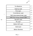
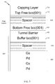
- Eine Senkrecht-Magnettunnelkontakt- bzw. MTJ-Vorrichtung (MTJ = magnetic tunnel junction) (102, 202, 302), die Folgendes aufweist:eine Tunnelbarriereschicht (106, 206, 306), die zwischen einer freien Schicht (108, 208, 308) und einer Referenzschicht abgeschieden ist;eine Tunnel-Magnetwiderstands- bzw. TMR-Verstärkungspufferschicht (TMR = tunnel magnetoresistance) (124, 224), die zwischen der Tunnelbarriereschicht und der Referenzschicht abgeschieden ist; undeinen amorphen Legierungs-TMR-Verstärkungsabstandshalter (122, 222), der zwischen der TMR- Verstärkungspufferschicht und der Referenzschicht abgeschieden ist.
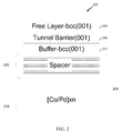
- Vorrichtung nach Anspruch 1, in der der TMR-Verstärkungsabstandshalter Folgendes aufweist:ein Supergitter bzw. eine Überstruktur oder eine Legierung aus Fe/Ta, Co/Ta, FeB/Ta, Fe/TaN und/oder FeB/TaN.
- Vorrichtung nach Anspruch 1, in der der TMR-Verstärkungsabstandshalter zwischen ungefähr 0,4nm und ungefähr 2nm dick ist.
- Vorrichtung nach Anspruch 1, die in ein Mobiltelefon, eine Set-Top-Box, eine Musikabspielvorrichtung, eine Videoabspielvorrichtung, eine Unterhaltungseinheit, eine Navigationseinrichtung, einen Computer, eine in der Hand zu haltende, persönliche Kommunikationssystem- bzw. PCS-Einheit (PCS = personal communication system), eine tragbare Dateneinheit und/oder eine Dateneinheit mit festem Standort integriert ist.
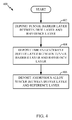
- Ein Verfahren (400) zum Einrichten bzw. Herstellen einer Senkrecht-Magnettunnelkontakt- bzw. -MTJ-Vorrichtung (MTJ = magnetic tunnel junction), das Folgendes aufweist:Abscheiden bzw. Ablagern (402, 502) einer Tunnelbarriereschicht zwischen einer freien Schicht und einer Referenzschicht;Abscheiden (404) einer Tunnelmagnetwiderstands- bzw. TMR-Verstärkungspufferschicht zwischen der Tunnelbarriereschicht und der Referenzschicht; undAbscheiden (406) eines amorphen Legierungs-TMR-Abstandshalters zwischen der TMR-Verstärkungspufferschicht und der Referenzschicht.
- Verfahren nach Anspruch 5, das weiter Folgendes aufweist:Abscheiden eines Supergitters bzw. einer Überstruktur oder einer Legierung aus Fe/Ta, Co/Ta, FeB/Ta, Fe/TaN und/oder FeB/TaN zwischen der TMR-Verstärkungspufferschicht und der Referenzschicht.
- Verfahren nach Anspruch 5, das weiter Folgendes aufweist:Abscheiden des amorphen Legierungs-TMR-Verstärkungsabstandshalters mit einer Dicke zwischen ungefähr 0,4nm und ungefähr 2nm.
- Vorrichtung nach Anspruch 1, wobei:die freie Schicht eine untere freie Schicht ist;,die weiter Folgendes aufweist:einen amorphen Legierungs-Senkrechtmagnetanisotropie- bzw. -PMA-Verstärkungsabstandshalter (PMA = perpendicular magnetic anisotropy) (310), der auf der unteren freien Schicht abgeschieden ist; undeine obere freie Schicht (312), die auf dem PMA-Verstärkungsabstandshalter abgeschieden ist.
- Vorrichtung nach Anspruch 8, die weiter Folgendes aufweist:eine isolierende Abdeckschicht (314), die direkt auf der oberen freien Schicht abgeschieden ist.
- Vorrichtung nach Anspruch 8, in der der PMA-Verstärkungsabstandshalter Folgendes aufweist:ein Supergitter bzw. eine Überstruktur oder eine Legierung aus Fe/Ta, Co/Ta, FeB/Ta, Fe/TaN und/oder FeB/TaN.
- Vorrichtung nach Anspruch 8, in der der PMA-Verstärkungsabstandshalter zwischen ungefähr 0,4nm und 1,5nm dick ist.
- Verfahren nach Anspruch 5, wobei die freie Schicht eine untere freie Schicht ist, das weiter Folgendes aufweist:Abscheiden (504) eines amorphen Legierungs-Senkrecht-Magnetanisotropie-bzw. PMA-Verstärkungsabstandshalters auf der unteren freien Schicht; undAbscheiden (506) einer oberen freien Schicht auf dem PMA-Verstärkungsabstandshalter.
- Verfahren nach Anspruch 12, das weiter Folgendes aufweist:Abscheiden einer isolierenden Abdeckschicht direkt auf der oberen freien Schicht.
- Verfahren nach Anspruch 12, das weiter Folgendes aufweist:Abscheiden eines Supergitters bzw. einer Überstruktur oder einre Legierung aus Fe/Ta, Co/Ta, FeB/Ta, Fe/TaN und/oder FeB/TaN zwischen der unteren freien Schicht und der oberen freien Schicht, um den amorphen Legierungs-PMA-Verstärkungsabstandshalter zu bilden.
- Verfahren nach Anspruch 12, das weiter Folgendes aufweist:Abscheiden des amorphen Legierungs-PMA-Verstärkungsabstandshalters mit einer Dicke zwischen ungefähr 0,4nm und 2nm.
Applications Claiming Priority (3)
| Application Number | Priority Date | Filing Date | Title |
|---|---|---|---|
| US201261676487P | 2012-07-27 | 2012-07-27 | |
| US13/770,526 US9214624B2 (en) | 2012-07-27 | 2013-02-19 | Amorphous spacerlattice spacer for perpendicular MTJs |
| PCT/US2013/052383 WO2014018920A1 (en) | 2012-07-27 | 2013-07-26 | Amorphous alloy spacer for perpendicular mtjs |
Publications (2)
| Publication Number | Publication Date |
|---|---|
| EP2878017A1 EP2878017A1 (de) | 2015-06-03 |
| EP2878017B1 true EP2878017B1 (de) | 2016-08-24 |
Family
ID=49994074
Family Applications (1)
| Application Number | Title | Priority Date | Filing Date |
|---|---|---|---|
| EP13747577.8A Active EP2878017B1 (de) | 2012-07-27 | 2013-07-26 | Abstandshalter aus amorpher legierung für senkrechte magnettunnelübergangselemente |
Country Status (5)
| Country | Link |
|---|---|
| US (2) | US9214624B2 (de) |
| EP (1) | EP2878017B1 (de) |
| CN (1) | CN104488102B (de) |
| IN (1) | IN2015MN00034A (de) |
| WO (1) | WO2014018920A1 (de) |
Cited By (1)
| Publication number | Priority date | Publication date | Assignee | Title |
|---|---|---|---|---|
| WO2021011144A1 (en) * | 2019-07-16 | 2021-01-21 | Applied Materials, Inc. | Magnetic tunnel junction stack with data retention |
Families Citing this family (122)
| Publication number | Priority date | Publication date | Assignee | Title |
|---|---|---|---|---|
| US8922956B2 (en) * | 2010-06-04 | 2014-12-30 | Seagate Technology Llc | Tunneling magneto-resistive sensors with buffer layers |
| US9007818B2 (en) | 2012-03-22 | 2015-04-14 | Micron Technology, Inc. | Memory cells, semiconductor device structures, systems including such cells, and methods of fabrication |
| US8923038B2 (en) | 2012-06-19 | 2014-12-30 | Micron Technology, Inc. | Memory cells, semiconductor device structures, memory systems, and methods of fabrication |
| US9054030B2 (en) | 2012-06-19 | 2015-06-09 | Micron Technology, Inc. | Memory cells, semiconductor device structures, memory systems, and methods of fabrication |
| US9214624B2 (en) | 2012-07-27 | 2015-12-15 | Qualcomm Incorporated | Amorphous spacerlattice spacer for perpendicular MTJs |
| KR102105078B1 (ko) * | 2013-05-30 | 2020-04-27 | 삼성전자주식회사 | 자기 기억 소자 |
| US9368714B2 (en) | 2013-07-01 | 2016-06-14 | Micron Technology, Inc. | Memory cells, methods of operation and fabrication, semiconductor device structures, and memory systems |
| US9466787B2 (en) | 2013-07-23 | 2016-10-11 | Micron Technology, Inc. | Memory cells, methods of fabrication, semiconductor device structures, memory systems, and electronic systems |
| US9240547B2 (en) | 2013-09-10 | 2016-01-19 | Micron Technology, Inc. | Magnetic tunnel junctions and methods of forming magnetic tunnel junctions |
| US9461242B2 (en) | 2013-09-13 | 2016-10-04 | Micron Technology, Inc. | Magnetic memory cells, methods of fabrication, semiconductor devices, memory systems, and electronic systems |
| US9608197B2 (en) | 2013-09-18 | 2017-03-28 | Micron Technology, Inc. | Memory cells, methods of fabrication, and semiconductor devices |
| TWI569484B (zh) * | 2014-01-24 | 2017-02-01 | 國立臺灣大學 | 具超晶格勢壘之磁穿隧接面及包含具超晶格勢壘磁穿隧接面之裝置 |
| US9601687B2 (en) | 2014-02-12 | 2017-03-21 | Qualcomm Incorporated | Dual interface free layer with amorphous cap layer for perpendicular magnetic tunnel junction |
| US10454024B2 (en) | 2014-02-28 | 2019-10-22 | Micron Technology, Inc. | Memory cells, methods of fabrication, and memory devices |
| US9583696B2 (en) | 2014-03-12 | 2017-02-28 | Qualcomm Incorporated | Reference layer for perpendicular magnetic anisotropy magnetic tunnel junction |
| US9281466B2 (en) | 2014-04-09 | 2016-03-08 | Micron Technology, Inc. | Memory cells, semiconductor structures, semiconductor devices, and methods of fabrication |
| US9269888B2 (en) | 2014-04-18 | 2016-02-23 | Micron Technology, Inc. | Memory cells, methods of fabrication, and semiconductor devices |
| EP3198601A4 (de) | 2014-09-26 | 2018-06-06 | INTEL Corporation | Amorphe keimschicht für verbesserte stabilität in einem senkrechten sttm-stapel |
| US9349945B2 (en) | 2014-10-16 | 2016-05-24 | Micron Technology, Inc. | Memory cells, semiconductor devices, and methods of fabrication |
| US9768377B2 (en) | 2014-12-02 | 2017-09-19 | Micron Technology, Inc. | Magnetic cell structures, and methods of fabrication |
| US9373779B1 (en) * | 2014-12-08 | 2016-06-21 | Micron Technology, Inc. | Magnetic tunnel junctions |
| US9634237B2 (en) * | 2014-12-23 | 2017-04-25 | Qualcomm Incorporated | Ultrathin perpendicular pinned layer structure for magnetic tunneling junction devices |
| US10439131B2 (en) | 2015-01-15 | 2019-10-08 | Micron Technology, Inc. | Methods of forming semiconductor devices including tunnel barrier materials |
| US9876163B2 (en) | 2015-03-05 | 2018-01-23 | Globalfoundries Singapore Pte. Ltd. | Magnetic memory with tunneling magnetoresistance enhanced spacer layer |
| US9666640B2 (en) | 2015-03-16 | 2017-05-30 | Globalfoundries Singapore Pte. Ltd. | High thermal budget magnetic memory |
| US10128309B2 (en) | 2015-03-27 | 2018-11-13 | Globalfoundries Singapore Pte. Ltd. | Storage layer for magnetic memory with high thermal stability |
| US9502642B2 (en) | 2015-04-10 | 2016-11-22 | Micron Technology, Inc. | Magnetic tunnel junctions, methods used while forming magnetic tunnel junctions, and methods of forming magnetic tunnel junctions |
| US9520553B2 (en) | 2015-04-15 | 2016-12-13 | Micron Technology, Inc. | Methods of forming a magnetic electrode of a magnetic tunnel junction and methods of forming a magnetic tunnel junction |
| US9530959B2 (en) | 2015-04-15 | 2016-12-27 | Micron Technology, Inc. | Magnetic tunnel junctions |
| US10468590B2 (en) | 2015-04-21 | 2019-11-05 | Spin Memory, Inc. | High annealing temperature perpendicular magnetic anisotropy structure for magnetic random access memory |
| US9728712B2 (en) | 2015-04-21 | 2017-08-08 | Spin Transfer Technologies, Inc. | Spin transfer torque structure for MRAM devices having a spin current injection capping layer |
| US9257136B1 (en) | 2015-05-05 | 2016-02-09 | Micron Technology, Inc. | Magnetic tunnel junctions |
| US9960346B2 (en) | 2015-05-07 | 2018-05-01 | Micron Technology, Inc. | Magnetic tunnel junctions |
| US9853206B2 (en) | 2015-06-16 | 2017-12-26 | Spin Transfer Technologies, Inc. | Precessional spin current structure for MRAM |
| US9831419B2 (en) | 2015-07-13 | 2017-11-28 | Western Digital Technologies, Inc. | Magnetoresistive device with laminate insertion layer in the free layer |
| US9537088B1 (en) * | 2015-07-13 | 2017-01-03 | Micron Technology, Inc. | Magnetic tunnel junctions |
| US9773974B2 (en) | 2015-07-30 | 2017-09-26 | Spin Transfer Technologies, Inc. | Polishing stop layer(s) for processing arrays of semiconductor elements |
| US10163479B2 (en) | 2015-08-14 | 2018-12-25 | Spin Transfer Technologies, Inc. | Method and apparatus for bipolar memory write-verify |
| KR102482372B1 (ko) | 2015-10-15 | 2022-12-29 | 삼성전자주식회사 | 자기 저항 메모리 소자 및 그 제조 방법 |
| US10297745B2 (en) | 2015-11-02 | 2019-05-21 | Globalfoundries Singapore Pte. Ltd. | Composite spacer layer for magnetoresistive memory |
| US10050192B2 (en) * | 2015-12-11 | 2018-08-14 | Imec Vzw | Magnetic memory device having buffer layer |
| US9741926B1 (en) | 2016-01-28 | 2017-08-22 | Spin Transfer Technologies, Inc. | Memory cell having magnetic tunnel junction and thermal stability enhancement layer |
| US10361361B2 (en) * | 2016-04-08 | 2019-07-23 | International Business Machines Corporation | Thin reference layer for STT MRAM |
| US9680089B1 (en) | 2016-05-13 | 2017-06-13 | Micron Technology, Inc. | Magnetic tunnel junctions |
| US10546625B2 (en) | 2016-09-27 | 2020-01-28 | Spin Memory, Inc. | Method of optimizing write voltage based on error buffer occupancy |
| US10437491B2 (en) | 2016-09-27 | 2019-10-08 | Spin Memory, Inc. | Method of processing incomplete memory operations in a memory device during a power up sequence and a power down sequence using a dynamic redundancy register |
| US10460781B2 (en) | 2016-09-27 | 2019-10-29 | Spin Memory, Inc. | Memory device with a dual Y-multiplexer structure for performing two simultaneous operations on the same row of a memory bank |
| US10366774B2 (en) | 2016-09-27 | 2019-07-30 | Spin Memory, Inc. | Device with dynamic redundancy registers |
| US10991410B2 (en) | 2016-09-27 | 2021-04-27 | Spin Memory, Inc. | Bi-polar write scheme |
| US10446210B2 (en) | 2016-09-27 | 2019-10-15 | Spin Memory, Inc. | Memory instruction pipeline with a pre-read stage for a write operation for reducing power consumption in a memory device that uses dynamic redundancy registers |
| US10360964B2 (en) | 2016-09-27 | 2019-07-23 | Spin Memory, Inc. | Method of writing contents in memory during a power up sequence using a dynamic redundancy register in a memory device |
| US10818331B2 (en) | 2016-09-27 | 2020-10-27 | Spin Memory, Inc. | Multi-chip module for MRAM devices with levels of dynamic redundancy registers |
| US10437723B2 (en) | 2016-09-27 | 2019-10-08 | Spin Memory, Inc. | Method of flushing the contents of a dynamic redundancy register to a secure storage area during a power down in a memory device |
| CN108232003B (zh) * | 2016-12-21 | 2021-09-03 | 上海磁宇信息科技有限公司 | 一种垂直型磁电阻元件及其制造方法 |
| WO2018125244A1 (en) * | 2016-12-30 | 2018-07-05 | Intel Corporation | Perpendicular magnetic tunnel junction (pmtj) devices having thermally resistive layers |
| US9865801B1 (en) * | 2017-01-19 | 2018-01-09 | Globalfoundries Singapore Pte. Ltd. | Integrated circuits with magnetic tunnel junctions and methods for producing the same |
| US10665777B2 (en) | 2017-02-28 | 2020-05-26 | Spin Memory, Inc. | Precessional spin current structure with non-magnetic insertion layer for MRAM |
| US10672976B2 (en) | 2017-02-28 | 2020-06-02 | Spin Memory, Inc. | Precessional spin current structure with high in-plane magnetization for MRAM |
| WO2018182663A1 (en) * | 2017-03-31 | 2018-10-04 | Intel Corporation | Spintronic memory with metal oxide cap layer |
| US10032978B1 (en) | 2017-06-27 | 2018-07-24 | Spin Transfer Technologies, Inc. | MRAM with reduced stray magnetic fields |
| WO2019005083A1 (en) * | 2017-06-29 | 2019-01-03 | Intel Corporation | MAGNETIC TUNNEL JUNCTION DEVICE HAVING A CARBON-DOPED FILTER LAYER |
| US10489245B2 (en) | 2017-10-24 | 2019-11-26 | Spin Memory, Inc. | Forcing stuck bits, waterfall bits, shunt bits and low TMR bits to short during testing and using on-the-fly bit failure detection and bit redundancy remapping techniques to correct them |
| US10529439B2 (en) | 2017-10-24 | 2020-01-07 | Spin Memory, Inc. | On-the-fly bit failure detection and bit redundancy remapping techniques to correct for fixed bit defects |
| US10656994B2 (en) | 2017-10-24 | 2020-05-19 | Spin Memory, Inc. | Over-voltage write operation of tunnel magnet-resistance (“TMR”) memory device and correcting failure bits therefrom by using on-the-fly bit failure detection and bit redundancy remapping techniques |
| US10481976B2 (en) | 2017-10-24 | 2019-11-19 | Spin Memory, Inc. | Forcing bits as bad to widen the window between the distributions of acceptable high and low resistive bits thereby lowering the margin and increasing the speed of the sense amplifiers |
| US10811594B2 (en) | 2017-12-28 | 2020-10-20 | Spin Memory, Inc. | Process for hard mask development for MRAM pillar formation using photolithography |
| US10424726B2 (en) | 2017-12-28 | 2019-09-24 | Spin Memory, Inc. | Process for improving photoresist pillar adhesion during MRAM fabrication |
| US10891997B2 (en) | 2017-12-28 | 2021-01-12 | Spin Memory, Inc. | Memory array with horizontal source line and a virtual source line |
| US10395712B2 (en) | 2017-12-28 | 2019-08-27 | Spin Memory, Inc. | Memory array with horizontal source line and sacrificial bitline per virtual source |
| US10360962B1 (en) | 2017-12-28 | 2019-07-23 | Spin Memory, Inc. | Memory array with individually trimmable sense amplifiers |
| US10395711B2 (en) | 2017-12-28 | 2019-08-27 | Spin Memory, Inc. | Perpendicular source and bit lines for an MRAM array |
| US10270027B1 (en) | 2017-12-29 | 2019-04-23 | Spin Memory, Inc. | Self-generating AC current assist in orthogonal STT-MRAM |
| US10424723B2 (en) | 2017-12-29 | 2019-09-24 | Spin Memory, Inc. | Magnetic tunnel junction devices including an optimization layer |
| US10360961B1 (en) | 2017-12-29 | 2019-07-23 | Spin Memory, Inc. | AC current pre-charge write-assist in orthogonal STT-MRAM |
| US10236048B1 (en) | 2017-12-29 | 2019-03-19 | Spin Memory, Inc. | AC current write-assist in orthogonal STT-MRAM |
| US10236047B1 (en) | 2017-12-29 | 2019-03-19 | Spin Memory, Inc. | Shared oscillator (STNO) for MRAM array write-assist in orthogonal STT-MRAM |
| US10546624B2 (en) | 2017-12-29 | 2020-01-28 | Spin Memory, Inc. | Multi-port random access memory |
| US10840439B2 (en) | 2017-12-29 | 2020-11-17 | Spin Memory, Inc. | Magnetic tunnel junction (MTJ) fabrication methods and systems |
| US10886330B2 (en) | 2017-12-29 | 2021-01-05 | Spin Memory, Inc. | Memory device having overlapping magnetic tunnel junctions in compliance with a reference pitch |
| US10784439B2 (en) | 2017-12-29 | 2020-09-22 | Spin Memory, Inc. | Precessional spin current magnetic tunnel junction devices and methods of manufacture |
| US10199083B1 (en) | 2017-12-29 | 2019-02-05 | Spin Transfer Technologies, Inc. | Three-terminal MRAM with ac write-assist for low read disturb |
| US10367139B2 (en) | 2017-12-29 | 2019-07-30 | Spin Memory, Inc. | Methods of manufacturing magnetic tunnel junction devices |
| US10840436B2 (en) | 2017-12-29 | 2020-11-17 | Spin Memory, Inc. | Perpendicular magnetic anisotropy interface tunnel junction devices and methods of manufacture |
| US10236439B1 (en) | 2017-12-30 | 2019-03-19 | Spin Memory, Inc. | Switching and stability control for perpendicular magnetic tunnel junction device |
| US10319900B1 (en) | 2017-12-30 | 2019-06-11 | Spin Memory, Inc. | Perpendicular magnetic tunnel junction device with precessional spin current layer having a modulated moment density |
| US10339993B1 (en) | 2017-12-30 | 2019-07-02 | Spin Memory, Inc. | Perpendicular magnetic tunnel junction device with skyrmionic assist layers for free layer switching |
| US10229724B1 (en) | 2017-12-30 | 2019-03-12 | Spin Memory, Inc. | Microwave write-assist in series-interconnected orthogonal STT-MRAM devices |
| US10141499B1 (en) | 2017-12-30 | 2018-11-27 | Spin Transfer Technologies, Inc. | Perpendicular magnetic tunnel junction device with offset precessional spin current layer |
| US10255962B1 (en) | 2017-12-30 | 2019-04-09 | Spin Memory, Inc. | Microwave write-assist in orthogonal STT-MRAM |
| WO2019135744A1 (en) * | 2018-01-03 | 2019-07-11 | Intel Corporation | Filter layer for a perpendicular top synthetic antiferromagnet (saf) stack for a spin orbit torque (sot) memory |
| US10468588B2 (en) | 2018-01-05 | 2019-11-05 | Spin Memory, Inc. | Perpendicular magnetic tunnel junction device with skyrmionic enhancement layers for the precessional spin current magnetic layer |
| US10438995B2 (en) | 2018-01-08 | 2019-10-08 | Spin Memory, Inc. | Devices including magnetic tunnel junctions integrated with selectors |
| US10438996B2 (en) | 2018-01-08 | 2019-10-08 | Spin Memory, Inc. | Methods of fabricating magnetic tunnel junctions integrated with selectors |
| US10446744B2 (en) | 2018-03-08 | 2019-10-15 | Spin Memory, Inc. | Magnetic tunnel junction wafer adaptor used in magnetic annealing furnace and method of using the same |
| US10784437B2 (en) | 2018-03-23 | 2020-09-22 | Spin Memory, Inc. | Three-dimensional arrays with MTJ devices including a free magnetic trench layer and a planar reference magnetic layer |
| US11107978B2 (en) | 2018-03-23 | 2021-08-31 | Spin Memory, Inc. | Methods of manufacturing three-dimensional arrays with MTJ devices including a free magnetic trench layer and a planar reference magnetic layer |
| US11107974B2 (en) | 2018-03-23 | 2021-08-31 | Spin Memory, Inc. | Magnetic tunnel junction devices including a free magnetic trench layer and a planar reference magnetic layer |
| US10529915B2 (en) | 2018-03-23 | 2020-01-07 | Spin Memory, Inc. | Bit line structures for three-dimensional arrays with magnetic tunnel junction devices including an annular free magnetic layer and a planar reference magnetic layer |
| US10411185B1 (en) | 2018-05-30 | 2019-09-10 | Spin Memory, Inc. | Process for creating a high density magnetic tunnel junction array test platform |
| US10559338B2 (en) | 2018-07-06 | 2020-02-11 | Spin Memory, Inc. | Multi-bit cell read-out techniques |
| US10593396B2 (en) | 2018-07-06 | 2020-03-17 | Spin Memory, Inc. | Multi-bit cell read-out techniques for MRAM cells with mixed pinned magnetization orientations |
| US10600478B2 (en) | 2018-07-06 | 2020-03-24 | Spin Memory, Inc. | Multi-bit cell read-out techniques for MRAM cells with mixed pinned magnetization orientations |
| US10692569B2 (en) | 2018-07-06 | 2020-06-23 | Spin Memory, Inc. | Read-out techniques for multi-bit cells |
| US11763972B2 (en) | 2018-08-12 | 2023-09-19 | HeFeChip Corporation Limited | Magnetic tunnel junction element with a robust reference layer |
| US10650875B2 (en) | 2018-08-21 | 2020-05-12 | Spin Memory, Inc. | System for a wide temperature range nonvolatile memory |
| US10818346B2 (en) | 2018-09-17 | 2020-10-27 | Northrop Grumman Systems Corporation | Quantizing loop memory cell system |
| US10699761B2 (en) | 2018-09-18 | 2020-06-30 | Spin Memory, Inc. | Word line decoder memory architecture |
| US11195991B2 (en) | 2018-09-27 | 2021-12-07 | Taiwan Semiconductor Manufacturing Company, Ltd. | Magnetic random access memory assisted devices and methods of making |
| US11621293B2 (en) | 2018-10-01 | 2023-04-04 | Integrated Silicon Solution, (Cayman) Inc. | Multi terminal device stack systems and methods |
| US10971680B2 (en) | 2018-10-01 | 2021-04-06 | Spin Memory, Inc. | Multi terminal device stack formation methods |
| US10580827B1 (en) | 2018-11-16 | 2020-03-03 | Spin Memory, Inc. | Adjustable stabilizer/polarizer method for MRAM with enhanced stability and efficient switching |
| US11107979B2 (en) | 2018-12-28 | 2021-08-31 | Spin Memory, Inc. | Patterned silicide structures and methods of manufacture |
| US11211117B2 (en) | 2019-01-24 | 2021-12-28 | Northrop Grumman Systems Corporation | Ferrimagnetic/ferromagnetic exchange bilayers for use as a fixed magnetic layer in a superconducting-based memory device |
| US10885974B2 (en) | 2019-01-30 | 2021-01-05 | Northrop Grumman Systems Corporation | Superconducting switch |
| US10879447B2 (en) | 2019-03-13 | 2020-12-29 | Northrop Grumman Systems Corporation | Repeating alternating multilayer buffer layer |
| CN111864057A (zh) * | 2019-04-29 | 2020-10-30 | 上海磁宇信息科技有限公司 | 一种磁性随机存取器及磁隧道结存储单元 |
| CN112635651A (zh) * | 2019-10-08 | 2021-04-09 | 上海磁宇信息科技有限公司 | 磁性隧道结结构及磁性随机存储器 |
| CN112864313B (zh) * | 2019-11-28 | 2023-03-21 | 上海磁宇信息科技有限公司 | 磁性随机存储器的磁性隧道结结构 |
| CN112928201B (zh) * | 2019-12-05 | 2023-04-07 | 上海磁宇信息科技有限公司 | 具有晶格传输作用的合成反铁层的磁性隧道结结构 |
| US11024791B1 (en) | 2020-01-27 | 2021-06-01 | Northrop Grumman Systems Corporation | Magnetically stabilized magnetic Josephson junction memory cell |
| US11342491B2 (en) | 2020-09-28 | 2022-05-24 | Northrop Grumman Systems Corporation | Magnetic Josephson junction system |
| US11444233B1 (en) | 2021-03-31 | 2022-09-13 | Northrop Grumman Systems Corporation | Josephson magnetic memory cell with ferrimagnetic layers having orthogonal magnetic polarity |
Family Cites Families (20)
| Publication number | Priority date | Publication date | Assignee | Title |
|---|---|---|---|---|
| JPS58141433A (ja) * | 1982-02-16 | 1983-08-22 | Teijin Ltd | 磁気記録媒体とその製造方法 |
| US6635496B2 (en) * | 2001-10-12 | 2003-10-21 | Infineon Technologies, Ag | Plate-through hard mask for MRAM devices |
| US6723450B2 (en) * | 2002-03-19 | 2004-04-20 | Hitachi Global Storage Technologies Netherlands B.V. | Magnetic recording medium with antiparallel coupled ferromagnetic films as the recording layer |
| US6831312B2 (en) * | 2002-08-30 | 2004-12-14 | Freescale Semiconductor, Inc. | Amorphous alloys for magnetic devices |
| US6870714B2 (en) * | 2003-03-12 | 2005-03-22 | Micron Technology, Inc. | Oxide buffer layer for improved magnetic tunnel junctions |
| JP2007273504A (ja) * | 2006-03-30 | 2007-10-18 | Fujitsu Ltd | 磁気抵抗効果素子、磁気ヘッド、磁気記録装置、磁気ランダムアクセスメモリ |
| US8623452B2 (en) | 2010-12-10 | 2014-01-07 | Avalanche Technology, Inc. | Magnetic random access memory (MRAM) with enhanced magnetic stiffness and method of making same |
| JP2008252008A (ja) | 2007-03-30 | 2008-10-16 | Toshiba Corp | 磁気抵抗効果素子、およびその製造方法 |
| JP4649457B2 (ja) * | 2007-09-26 | 2011-03-09 | 株式会社東芝 | 磁気抵抗素子及び磁気メモリ |
| US8743593B2 (en) * | 2008-12-10 | 2014-06-03 | Hitachi, Ltd. | Magnetoresistance effect element and magnetic memory cell and magnetic random access memory using same |
| JP2011123944A (ja) * | 2009-12-10 | 2011-06-23 | Hitachi Global Storage Technologies Netherlands Bv | Tmrリード・ヘッドの製造方法及びtmr積層体 |
| KR20110071710A (ko) | 2009-12-21 | 2011-06-29 | 삼성전자주식회사 | 수직 자기터널접합과 이를 포함하는 자성소자 및 그 제조방법 |
| US9385308B2 (en) | 2010-03-26 | 2016-07-05 | Qualcomm Incorporated | Perpendicular magnetic tunnel junction structure |
| US8564080B2 (en) | 2010-07-16 | 2013-10-22 | Qualcomm Incorporated | Magnetic storage element utilizing improved pinned layer stack |
| JP5148673B2 (ja) * | 2010-09-17 | 2013-02-20 | 株式会社東芝 | 磁気抵抗効果素子及び磁気メモリ |
| US20120104522A1 (en) | 2010-11-01 | 2012-05-03 | Seagate Technology Llc | Magnetic tunnel junction cells having perpendicular anisotropy and enhancement layer |
| US20120267733A1 (en) * | 2011-04-25 | 2012-10-25 | International Business Machines Corporation | Magnetic stacks with perpendicular magnetic anisotropy for spin momentum transfer magnetoresistive random access memory |
| CN102364618B (zh) * | 2011-11-10 | 2013-03-06 | 中国科学院物理研究所 | 一种具有垂直磁各向异性的多层膜材料 |
| US8871365B2 (en) * | 2012-02-28 | 2014-10-28 | Headway Technologies, Inc. | High thermal stability reference structure with out-of-plane aniotropy to magnetic device applications |
| US9214624B2 (en) | 2012-07-27 | 2015-12-15 | Qualcomm Incorporated | Amorphous spacerlattice spacer for perpendicular MTJs |
-
2013
- 2013-02-19 US US13/770,526 patent/US9214624B2/en active Active
- 2013-07-26 WO PCT/US2013/052383 patent/WO2014018920A1/en active Application Filing
- 2013-07-26 IN IN34MUN2015 patent/IN2015MN00034A/en unknown
- 2013-07-26 CN CN201380039270.7A patent/CN104488102B/zh active Active
- 2013-07-26 EP EP13747577.8A patent/EP2878017B1/de active Active
-
2015
- 2015-11-13 US US14/940,996 patent/US9548445B2/en active Active
Cited By (1)
| Publication number | Priority date | Publication date | Assignee | Title |
|---|---|---|---|---|
| WO2021011144A1 (en) * | 2019-07-16 | 2021-01-21 | Applied Materials, Inc. | Magnetic tunnel junction stack with data retention |
Also Published As
| Publication number | Publication date |
|---|---|
| EP2878017A1 (de) | 2015-06-03 |
| IN2015MN00034A (de) | 2015-10-16 |
| US20140027869A1 (en) | 2014-01-30 |
| WO2014018920A1 (en) | 2014-01-30 |
| US9214624B2 (en) | 2015-12-15 |
| US20160111634A1 (en) | 2016-04-21 |
| CN104488102B (zh) | 2017-05-03 |
| CN104488102A (zh) | 2015-04-01 |
| US9548445B2 (en) | 2017-01-17 |
Similar Documents
| Publication | Publication Date | Title |
|---|---|---|
| US9548445B2 (en) | Amorphous alloy space for perpendicular MTJs | |
| US9935258B2 (en) | Thermally tolerant perpendicular magnetic anisotropy coupled elements for spin-transfer torque switching device | |
| US10103319B2 (en) | Ultrathin perpendicular pinned layer structure for magnetic tunneling junction devices | |
| US10121961B2 (en) | Magnetic devices including magnetic junctions having tilted easy axes and enhanced damping programmable using spin orbit torque | |
| JP6038451B2 (ja) | スピントランスファトルクメモリ用の挿入層を有する磁性層を提供するための方法及びシステム | |
| US8704320B2 (en) | Strain induced reduction of switching current in spin-transfer torque switching devices | |
| JP5961785B2 (ja) | スイッチングが改良されたハイブリッド磁気トンネル接合要素を提供するための方法およびシステム | |
| US8592929B2 (en) | Symmetrically switchable spin-transfer-torque magnetoresistive device | |
| US20120267736A1 (en) | Method And System For Providing A Magnetic Junction Having An Engineered Barrier Layer | |
| US20180108833A1 (en) | Method and system for providing magnetic junctions usable in spin transfer torque applications utilizing interstitial glass-forming agent(s) | |
| US20170141296A1 (en) | Method for providing a high perpendicular magnetic anisotropy layer in a magnetic junction usable in spin transfer torque magnetic devices using multiple anneals | |
| KR20180038944A (ko) | 자기 장치에 사용 가능한 자기 접합 및 그 제조 방법 |
Legal Events
| Date | Code | Title | Description |
|---|---|---|---|
| PUAI | Public reference made under article 153(3) epc to a published international application that has entered the european phase |
Free format text: ORIGINAL CODE: 0009012 |
|
| 17P | Request for examination filed |
Effective date: 20150116 |
|
| AK | Designated contracting states |
Kind code of ref document: A1 Designated state(s): AL AT BE BG CH CY CZ DE DK EE ES FI FR GB GR HR HU IE IS IT LI LT LU LV MC MK MT NL NO PL PT RO RS SE SI SK SM TR |
|
| AX | Request for extension of the european patent |
Extension state: BA ME |
|
| DAX | Request for extension of the european patent (deleted) | ||
| RIC1 | Information provided on ipc code assigned before grant |
Ipc: G11C 11/15 20060101ALI20151215BHEP Ipc: H01L 43/08 20060101AFI20151215BHEP Ipc: H01L 43/12 20060101ALI20151215BHEP |
|
| GRAP | Despatch of communication of intention to grant a patent |
Free format text: ORIGINAL CODE: EPIDOSNIGR1 |
|
| INTG | Intention to grant announced |
Effective date: 20160129 |
|
| GRAR | Information related to intention to grant a patent recorded |
Free format text: ORIGINAL CODE: EPIDOSNIGR71 |
|
| GRAS | Grant fee paid |
Free format text: ORIGINAL CODE: EPIDOSNIGR3 |
|
| GRAA | (expected) grant |
Free format text: ORIGINAL CODE: 0009210 |
|
| INTG | Intention to grant announced |
Effective date: 20160628 |
|
| AK | Designated contracting states |
Kind code of ref document: B1 Designated state(s): AL AT BE BG CH CY CZ DE DK EE ES FI FR GB GR HR HU IE IS IT LI LT LU LV MC MK MT NL NO PL PT RO RS SE SI SK SM TR |
|
| REG | Reference to a national code |
Ref country code: GB Ref legal event code: FG4D |
|
| REG | Reference to a national code |
Ref country code: CH Ref legal event code: EP |
|
| REG | Reference to a national code |
Ref country code: AT Ref legal event code: REF Ref document number: 823767 Country of ref document: AT Kind code of ref document: T Effective date: 20160915 |
|
| REG | Reference to a national code |
Ref country code: IE Ref legal event code: FG4D |
|
| REG | Reference to a national code |
Ref country code: DE Ref legal event code: R096 Ref document number: 602013010694 Country of ref document: DE |
|
| REG | Reference to a national code |
Ref country code: LT Ref legal event code: MG4D |
|
| REG | Reference to a national code |
Ref country code: NL Ref legal event code: MP Effective date: 20160824 |
|
| REG | Reference to a national code |
Ref country code: AT Ref legal event code: MK05 Ref document number: 823767 Country of ref document: AT Kind code of ref document: T Effective date: 20160824 |
|
| PG25 | Lapsed in a contracting state [announced via postgrant information from national office to epo] |
Ref country code: FI Free format text: LAPSE BECAUSE OF FAILURE TO SUBMIT A TRANSLATION OF THE DESCRIPTION OR TO PAY THE FEE WITHIN THE PRESCRIBED TIME-LIMIT Effective date: 20160824 Ref country code: NO Free format text: LAPSE BECAUSE OF FAILURE TO SUBMIT A TRANSLATION OF THE DESCRIPTION OR TO PAY THE FEE WITHIN THE PRESCRIBED TIME-LIMIT Effective date: 20161124 Ref country code: LT Free format text: LAPSE BECAUSE OF FAILURE TO SUBMIT A TRANSLATION OF THE DESCRIPTION OR TO PAY THE FEE WITHIN THE PRESCRIBED TIME-LIMIT Effective date: 20160824 Ref country code: IT Free format text: LAPSE BECAUSE OF FAILURE TO SUBMIT A TRANSLATION OF THE DESCRIPTION OR TO PAY THE FEE WITHIN THE PRESCRIBED TIME-LIMIT Effective date: 20160824 Ref country code: NL Free format text: LAPSE BECAUSE OF FAILURE TO SUBMIT A TRANSLATION OF THE DESCRIPTION OR TO PAY THE FEE WITHIN THE PRESCRIBED TIME-LIMIT Effective date: 20160824 Ref country code: HR Free format text: LAPSE BECAUSE OF FAILURE TO SUBMIT A TRANSLATION OF THE DESCRIPTION OR TO PAY THE FEE WITHIN THE PRESCRIBED TIME-LIMIT Effective date: 20160824 Ref country code: RS Free format text: LAPSE BECAUSE OF FAILURE TO SUBMIT A TRANSLATION OF THE DESCRIPTION OR TO PAY THE FEE WITHIN THE PRESCRIBED TIME-LIMIT Effective date: 20160824 |
|
| PG25 | Lapsed in a contracting state [announced via postgrant information from national office to epo] |
Ref country code: ES Free format text: LAPSE BECAUSE OF FAILURE TO SUBMIT A TRANSLATION OF THE DESCRIPTION OR TO PAY THE FEE WITHIN THE PRESCRIBED TIME-LIMIT Effective date: 20160824 Ref country code: AT Free format text: LAPSE BECAUSE OF FAILURE TO SUBMIT A TRANSLATION OF THE DESCRIPTION OR TO PAY THE FEE WITHIN THE PRESCRIBED TIME-LIMIT Effective date: 20160824 Ref country code: GR Free format text: LAPSE BECAUSE OF FAILURE TO SUBMIT A TRANSLATION OF THE DESCRIPTION OR TO PAY THE FEE WITHIN THE PRESCRIBED TIME-LIMIT Effective date: 20161125 Ref country code: LV Free format text: LAPSE BECAUSE OF FAILURE TO SUBMIT A TRANSLATION OF THE DESCRIPTION OR TO PAY THE FEE WITHIN THE PRESCRIBED TIME-LIMIT Effective date: 20160824 Ref country code: PT Free format text: LAPSE BECAUSE OF FAILURE TO SUBMIT A TRANSLATION OF THE DESCRIPTION OR TO PAY THE FEE WITHIN THE PRESCRIBED TIME-LIMIT Effective date: 20161226 Ref country code: SE Free format text: LAPSE BECAUSE OF FAILURE TO SUBMIT A TRANSLATION OF THE DESCRIPTION OR TO PAY THE FEE WITHIN THE PRESCRIBED TIME-LIMIT Effective date: 20160824 |
|
| PG25 | Lapsed in a contracting state [announced via postgrant information from national office to epo] |
Ref country code: EE Free format text: LAPSE BECAUSE OF FAILURE TO SUBMIT A TRANSLATION OF THE DESCRIPTION OR TO PAY THE FEE WITHIN THE PRESCRIBED TIME-LIMIT Effective date: 20160824 Ref country code: RO Free format text: LAPSE BECAUSE OF FAILURE TO SUBMIT A TRANSLATION OF THE DESCRIPTION OR TO PAY THE FEE WITHIN THE PRESCRIBED TIME-LIMIT Effective date: 20160824 |
|
| REG | Reference to a national code |
Ref country code: DE Ref legal event code: R097 Ref document number: 602013010694 Country of ref document: DE |
|
| PG25 | Lapsed in a contracting state [announced via postgrant information from national office to epo] |
Ref country code: CZ Free format text: LAPSE BECAUSE OF FAILURE TO SUBMIT A TRANSLATION OF THE DESCRIPTION OR TO PAY THE FEE WITHIN THE PRESCRIBED TIME-LIMIT Effective date: 20160824 Ref country code: SM Free format text: LAPSE BECAUSE OF FAILURE TO SUBMIT A TRANSLATION OF THE DESCRIPTION OR TO PAY THE FEE WITHIN THE PRESCRIBED TIME-LIMIT Effective date: 20160824 Ref country code: BE Free format text: LAPSE BECAUSE OF FAILURE TO SUBMIT A TRANSLATION OF THE DESCRIPTION OR TO PAY THE FEE WITHIN THE PRESCRIBED TIME-LIMIT Effective date: 20160824 Ref country code: DK Free format text: LAPSE BECAUSE OF FAILURE TO SUBMIT A TRANSLATION OF THE DESCRIPTION OR TO PAY THE FEE WITHIN THE PRESCRIBED TIME-LIMIT Effective date: 20160824 Ref country code: BG Free format text: LAPSE BECAUSE OF FAILURE TO SUBMIT A TRANSLATION OF THE DESCRIPTION OR TO PAY THE FEE WITHIN THE PRESCRIBED TIME-LIMIT Effective date: 20161124 Ref country code: PL Free format text: LAPSE BECAUSE OF FAILURE TO SUBMIT A TRANSLATION OF THE DESCRIPTION OR TO PAY THE FEE WITHIN THE PRESCRIBED TIME-LIMIT Effective date: 20160824 Ref country code: SK Free format text: LAPSE BECAUSE OF FAILURE TO SUBMIT A TRANSLATION OF THE DESCRIPTION OR TO PAY THE FEE WITHIN THE PRESCRIBED TIME-LIMIT Effective date: 20160824 |
|
| REG | Reference to a national code |
Ref country code: FR Ref legal event code: PLFP Year of fee payment: 5 |
|
| PLBE | No opposition filed within time limit |
Free format text: ORIGINAL CODE: 0009261 |
|
| STAA | Information on the status of an ep patent application or granted ep patent |
Free format text: STATUS: NO OPPOSITION FILED WITHIN TIME LIMIT |
|
| 26N | No opposition filed |
Effective date: 20170526 |
|
| PG25 | Lapsed in a contracting state [announced via postgrant information from national office to epo] |
Ref country code: SI Free format text: LAPSE BECAUSE OF FAILURE TO SUBMIT A TRANSLATION OF THE DESCRIPTION OR TO PAY THE FEE WITHIN THE PRESCRIBED TIME-LIMIT Effective date: 20160824 |
|
| REG | Reference to a national code |
Ref country code: CH Ref legal event code: PL |
|
| REG | Reference to a national code |
Ref country code: IE Ref legal event code: MM4A |
|
| PG25 | Lapsed in a contracting state [announced via postgrant information from national office to epo] |
Ref country code: LI Free format text: LAPSE BECAUSE OF NON-PAYMENT OF DUE FEES Effective date: 20170731 Ref country code: IE Free format text: LAPSE BECAUSE OF NON-PAYMENT OF DUE FEES Effective date: 20170726 Ref country code: CH Free format text: LAPSE BECAUSE OF NON-PAYMENT OF DUE FEES Effective date: 20170731 |
|
| REG | Reference to a national code |
Ref country code: FR Ref legal event code: PLFP Year of fee payment: 6 |
|
| PG25 | Lapsed in a contracting state [announced via postgrant information from national office to epo] |
Ref country code: LU Free format text: LAPSE BECAUSE OF NON-PAYMENT OF DUE FEES Effective date: 20170726 |
|
| PGFP | Annual fee paid to national office [announced via postgrant information from national office to epo] |
Ref country code: FR Payment date: 20180620 Year of fee payment: 6 |
|
| PG25 | Lapsed in a contracting state [announced via postgrant information from national office to epo] |
Ref country code: MT Free format text: LAPSE BECAUSE OF NON-PAYMENT OF DUE FEES Effective date: 20170726 |
|
| PG25 | Lapsed in a contracting state [announced via postgrant information from national office to epo] |
Ref country code: AL Free format text: LAPSE BECAUSE OF FAILURE TO SUBMIT A TRANSLATION OF THE DESCRIPTION OR TO PAY THE FEE WITHIN THE PRESCRIBED TIME-LIMIT Effective date: 20160824 |
|
| PGFP | Annual fee paid to national office [announced via postgrant information from national office to epo] |
Ref country code: GB Payment date: 20180625 Year of fee payment: 6 |
|
| PG25 | Lapsed in a contracting state [announced via postgrant information from national office to epo] |
Ref country code: HU Free format text: LAPSE BECAUSE OF FAILURE TO SUBMIT A TRANSLATION OF THE DESCRIPTION OR TO PAY THE FEE WITHIN THE PRESCRIBED TIME-LIMIT; INVALID AB INITIO Effective date: 20130726 Ref country code: MC Free format text: LAPSE BECAUSE OF FAILURE TO SUBMIT A TRANSLATION OF THE DESCRIPTION OR TO PAY THE FEE WITHIN THE PRESCRIBED TIME-LIMIT Effective date: 20160824 |
|
| PG25 | Lapsed in a contracting state [announced via postgrant information from national office to epo] |
Ref country code: CY Free format text: LAPSE BECAUSE OF FAILURE TO SUBMIT A TRANSLATION OF THE DESCRIPTION OR TO PAY THE FEE WITHIN THE PRESCRIBED TIME-LIMIT Effective date: 20160824 |
|
| PG25 | Lapsed in a contracting state [announced via postgrant information from national office to epo] |
Ref country code: MK Free format text: LAPSE BECAUSE OF FAILURE TO SUBMIT A TRANSLATION OF THE DESCRIPTION OR TO PAY THE FEE WITHIN THE PRESCRIBED TIME-LIMIT Effective date: 20160824 |
|
| GBPC | Gb: european patent ceased through non-payment of renewal fee |
Effective date: 20190726 |
|
| PG25 | Lapsed in a contracting state [announced via postgrant information from national office to epo] |
Ref country code: TR Free format text: LAPSE BECAUSE OF FAILURE TO SUBMIT A TRANSLATION OF THE DESCRIPTION OR TO PAY THE FEE WITHIN THE PRESCRIBED TIME-LIMIT Effective date: 20160824 |
|
| PG25 | Lapsed in a contracting state [announced via postgrant information from national office to epo] |
Ref country code: GB Free format text: LAPSE BECAUSE OF NON-PAYMENT OF DUE FEES Effective date: 20190726 |
|
| PG25 | Lapsed in a contracting state [announced via postgrant information from national office to epo] |
Ref country code: FR Free format text: LAPSE BECAUSE OF NON-PAYMENT OF DUE FEES Effective date: 20190731 |
|
| PG25 | Lapsed in a contracting state [announced via postgrant information from national office to epo] |
Ref country code: IS Free format text: LAPSE BECAUSE OF FAILURE TO SUBMIT A TRANSLATION OF THE DESCRIPTION OR TO PAY THE FEE WITHIN THE PRESCRIBED TIME-LIMIT Effective date: 20161224 |
|
| REG | Reference to a national code |
Ref country code: DE Ref legal event code: R082 Ref document number: 602013010694 Country of ref document: DE Representative=s name: MAUCHER JENKINS PATENTANWAELTE & RECHTSANWAELT, DE |
|
| REG | Reference to a national code |
Ref country code: DE Ref legal event code: R079 Ref document number: 602013010694 Country of ref document: DE Free format text: PREVIOUS MAIN CLASS: H01L0043080000 Ipc: H10N0050100000 |
|
| PGFP | Annual fee paid to national office [announced via postgrant information from national office to epo] |
Ref country code: DE Payment date: 20230614 Year of fee payment: 11 |