EP2876983A2 - Electronic device and method for assembling the same - Google Patents
Electronic device and method for assembling the same Download PDFInfo
- Publication number
- EP2876983A2 EP2876983A2 EP14194157.5A EP14194157A EP2876983A2 EP 2876983 A2 EP2876983 A2 EP 2876983A2 EP 14194157 A EP14194157 A EP 14194157A EP 2876983 A2 EP2876983 A2 EP 2876983A2
- Authority
- EP
- European Patent Office
- Prior art keywords
- heat
- component
- dissipating component
- elastic clip
- dissipating
- Prior art date
- Legal status (The legal status is an assumption and is not a legal conclusion. Google has not performed a legal analysis and makes no representation as to the accuracy of the status listed.)
- Granted
Links
Images






Classifications
-
- H—ELECTRICITY
- H05—ELECTRIC TECHNIQUES NOT OTHERWISE PROVIDED FOR
- H05K—PRINTED CIRCUITS; CASINGS OR CONSTRUCTIONAL DETAILS OF ELECTRIC APPARATUS; MANUFACTURE OF ASSEMBLAGES OF ELECTRICAL COMPONENTS
- H05K7/00—Constructional details common to different types of electric apparatus
- H05K7/14—Mounting supporting structure in casing or on frame or rack
- H05K7/1422—Printed circuit boards receptacles, e.g. stacked structures, electronic circuit modules or box like frames
- H05K7/1427—Housings
- H05K7/1432—Housings specially adapted for power drive units or power converters
- H05K7/14322—Housings specially adapted for power drive units or power converters wherein the control and power circuits of a power converter are arranged within the same casing
-
- B—PERFORMING OPERATIONS; TRANSPORTING
- B60—VEHICLES IN GENERAL
- B60L—PROPULSION OF ELECTRICALLY-PROPELLED VEHICLES; SUPPLYING ELECTRIC POWER FOR AUXILIARY EQUIPMENT OF ELECTRICALLY-PROPELLED VEHICLES; ELECTRODYNAMIC BRAKE SYSTEMS FOR VEHICLES IN GENERAL; MAGNETIC SUSPENSION OR LEVITATION FOR VEHICLES; MONITORING OPERATING VARIABLES OF ELECTRICALLY-PROPELLED VEHICLES; ELECTRIC SAFETY DEVICES FOR ELECTRICALLY-PROPELLED VEHICLES
- B60L1/00—Supplying electric power to auxiliary equipment of vehicles
-
- B—PERFORMING OPERATIONS; TRANSPORTING
- B60—VEHICLES IN GENERAL
- B60L—PROPULSION OF ELECTRICALLY-PROPELLED VEHICLES; SUPPLYING ELECTRIC POWER FOR AUXILIARY EQUIPMENT OF ELECTRICALLY-PROPELLED VEHICLES; ELECTRODYNAMIC BRAKE SYSTEMS FOR VEHICLES IN GENERAL; MAGNETIC SUSPENSION OR LEVITATION FOR VEHICLES; MONITORING OPERATING VARIABLES OF ELECTRICALLY-PROPELLED VEHICLES; ELECTRIC SAFETY DEVICES FOR ELECTRICALLY-PROPELLED VEHICLES
- B60L7/00—Electrodynamic brake systems for vehicles in general
-
- H—ELECTRICITY
- H02—GENERATION; CONVERSION OR DISTRIBUTION OF ELECTRIC POWER
- H02M—APPARATUS FOR CONVERSION BETWEEN AC AND AC, BETWEEN AC AND DC, OR BETWEEN DC AND DC, AND FOR USE WITH MAINS OR SIMILAR POWER SUPPLY SYSTEMS; CONVERSION OF DC OR AC INPUT POWER INTO SURGE OUTPUT POWER; CONTROL OR REGULATION THEREOF
- H02M3/00—Conversion of DC power input into DC power output
- H02M3/003—Constructional details, e.g. physical layout, assembly, wiring or busbar connections
-
- H—ELECTRICITY
- H05—ELECTRIC TECHNIQUES NOT OTHERWISE PROVIDED FOR
- H05K—PRINTED CIRCUITS; CASINGS OR CONSTRUCTIONAL DETAILS OF ELECTRIC APPARATUS; MANUFACTURE OF ASSEMBLAGES OF ELECTRICAL COMPONENTS
- H05K3/00—Apparatus or processes for manufacturing printed circuits
- H05K3/30—Assembling printed circuits with electric components, e.g. with resistors
- H05K3/32—Assembling printed circuits with electric components, e.g. with resistors electrically connecting electric components or wires to printed circuits
- H05K3/328—Assembling printed circuits with electric components, e.g. with resistors electrically connecting electric components or wires to printed circuits by welding
-
- H—ELECTRICITY
- H05—ELECTRIC TECHNIQUES NOT OTHERWISE PROVIDED FOR
- H05K—PRINTED CIRCUITS; CASINGS OR CONSTRUCTIONAL DETAILS OF ELECTRIC APPARATUS; MANUFACTURE OF ASSEMBLAGES OF ELECTRICAL COMPONENTS
- H05K5/00—Casings, cabinets or drawers for electric apparatus
- H05K5/0026—Casings, cabinets or drawers for electric apparatus provided with connectors and printed circuit boards [PCB], e.g. automotive electronic control units
- H05K5/0039—Casings, cabinets or drawers for electric apparatus provided with connectors and printed circuit boards [PCB], e.g. automotive electronic control units having a tubular housing wherein the PCB is inserted longitudinally
-
- H—ELECTRICITY
- H05—ELECTRIC TECHNIQUES NOT OTHERWISE PROVIDED FOR
- H05K—PRINTED CIRCUITS; CASINGS OR CONSTRUCTIONAL DETAILS OF ELECTRIC APPARATUS; MANUFACTURE OF ASSEMBLAGES OF ELECTRICAL COMPONENTS
- H05K7/00—Constructional details common to different types of electric apparatus
- H05K7/20—Modifications to facilitate cooling, ventilating, or heating
- H05K7/2039—Modifications to facilitate cooling, ventilating, or heating characterised by the heat transfer by conduction from the heat generating element to a dissipating body
- H05K7/20409—Outer radiating structures on heat dissipating housings, e.g. fins integrated with the housing
-
- H—ELECTRICITY
- H05—ELECTRIC TECHNIQUES NOT OTHERWISE PROVIDED FOR
- H05K—PRINTED CIRCUITS; CASINGS OR CONSTRUCTIONAL DETAILS OF ELECTRIC APPARATUS; MANUFACTURE OF ASSEMBLAGES OF ELECTRICAL COMPONENTS
- H05K7/00—Constructional details common to different types of electric apparatus
- H05K7/20—Modifications to facilitate cooling, ventilating, or heating
- H05K7/2089—Modifications to facilitate cooling, ventilating, or heating for power electronics, e.g. for inverters for controlling motor
- H05K7/209—Heat transfer by conduction from internal heat source to heat radiating structure
-
- H—ELECTRICITY
- H10—SEMICONDUCTOR DEVICES; ELECTRIC SOLID-STATE DEVICES NOT OTHERWISE PROVIDED FOR
- H10W—GENERIC PACKAGES, INTERCONNECTIONS, CONNECTORS OR OTHER CONSTRUCTIONAL DETAILS OF DEVICES COVERED BY CLASS H10
- H10W74/00—Encapsulations, e.g. protective coatings
- H10W74/40—Encapsulations, e.g. protective coatings characterised by their materials
-
- H—ELECTRICITY
- H05—ELECTRIC TECHNIQUES NOT OTHERWISE PROVIDED FOR
- H05K—PRINTED CIRCUITS; CASINGS OR CONSTRUCTIONAL DETAILS OF ELECTRIC APPARATUS; MANUFACTURE OF ASSEMBLAGES OF ELECTRICAL COMPONENTS
- H05K2203/00—Indexing scheme relating to apparatus or processes for manufacturing printed circuits covered by H05K3/00
- H05K2203/04—Soldering or other types of metallurgic bonding
-
- Y—GENERAL TAGGING OF NEW TECHNOLOGICAL DEVELOPMENTS; GENERAL TAGGING OF CROSS-SECTIONAL TECHNOLOGIES SPANNING OVER SEVERAL SECTIONS OF THE IPC; TECHNICAL SUBJECTS COVERED BY FORMER USPC CROSS-REFERENCE ART COLLECTIONS [XRACs] AND DIGESTS
- Y02—TECHNOLOGIES OR APPLICATIONS FOR MITIGATION OR ADAPTATION AGAINST CLIMATE CHANGE
- Y02T—CLIMATE CHANGE MITIGATION TECHNOLOGIES RELATED TO TRANSPORTATION
- Y02T90/00—Enabling technologies or technologies with a potential or indirect contribution to GHG emissions mitigation
- Y02T90/10—Technologies relating to charging of electric vehicles
- Y02T90/12—Electric charging stations
-
- Y—GENERAL TAGGING OF NEW TECHNOLOGICAL DEVELOPMENTS; GENERAL TAGGING OF CROSS-SECTIONAL TECHNOLOGIES SPANNING OVER SEVERAL SECTIONS OF THE IPC; TECHNICAL SUBJECTS COVERED BY FORMER USPC CROSS-REFERENCE ART COLLECTIONS [XRACs] AND DIGESTS
- Y10—TECHNICAL SUBJECTS COVERED BY FORMER USPC
- Y10T—TECHNICAL SUBJECTS COVERED BY FORMER US CLASSIFICATION
- Y10T29/00—Metal working
- Y10T29/49—Method of mechanical manufacture
- Y10T29/49002—Electrical device making
-
- Y—GENERAL TAGGING OF NEW TECHNOLOGICAL DEVELOPMENTS; GENERAL TAGGING OF CROSS-SECTIONAL TECHNOLOGIES SPANNING OVER SEVERAL SECTIONS OF THE IPC; TECHNICAL SUBJECTS COVERED BY FORMER USPC CROSS-REFERENCE ART COLLECTIONS [XRACs] AND DIGESTS
- Y10—TECHNICAL SUBJECTS COVERED BY FORMER USPC
- Y10T—TECHNICAL SUBJECTS COVERED BY FORMER US CLASSIFICATION
- Y10T29/00—Metal working
- Y10T29/49—Method of mechanical manufacture
- Y10T29/49002—Electrical device making
- Y10T29/49117—Conductor or circuit manufacturing
- Y10T29/49124—On flat or curved insulated base, e.g., printed circuit, etc.
- Y10T29/4913—Assembling to base an electrical component, e.g., capacitor, etc.
- Y10T29/49144—Assembling to base an electrical component, e.g., capacitor, etc. by metal fusion
Definitions
- a hybrid electric vehicle or an electric vehicle has the advantages of economy, energy saving and environmental protection, etc., and has become the main focus of research and development for the major automobile companies under the crisis of energy shortage.
- vehicle amount has been increasing, and the pressure from the environmental pollution and the energy shortage has become obvious.
- countries around the world regard energy saving and environmental protection as the prior direction of development for the future automobile industry.
- electric vehicles have an incomparable superiority in the aspect of energy saving and environmental protection.
- the electric vehicles have achieved great improvements in the core technologies such as power battery, electrical motor, control system, and on board charger module.
- the safety, reliability, and lifetime of products are significantly raised, and the manufacturing cost is under a certain level of control.
- Hybrid electric vehicles and electric vehicles are gradually entering the stage of practical use and small industrialization, and will be the strategic direction of the development of the automobile industry.
- a charger module can be classified as an off board charger module and an on board charger module (OBCM).
- the off board charger module which is also referred to as a ground charging device or a charging pile, often has a larger power, larger volume, and greater mass.
- the OBCM is a device mounted on an electric vehicle for charging a battery pack by the AC power grid, in which an AC power cable is plugged into a socket of the electric vehicle to get it charged.
- the OBCM is essentially a power conversion device.
- the OBCM uses input wires to receive alternative current which is coupled to AC power grid, and outputs high voltage direct current to charge the on board high voltage battery pack, and uses a communication port to maintain real-time interactive communications with a battery management system (BMS).
- BMS battery management system
- the overall performance enhancement and the cost control of the OBCM are always key factors restricting the mass production of electric vehicles, and the structure design and the thermal management of the OBCM are ones of the most critical indicators for comprehensively evaluating the performance of the OB
- the OBCM or the power conversion device, consumes a lot of electricity
- the electronic components in the power conversion device generate quite a lot of heat with the increasing of power density of the OBCM or device, and if the electronic components do not physically contact the heat spreaders, the heat-dissipating efficiency is limited and the heat transferring performance is not good.
- This disclosure provides an electronic device and a method for assembling the same.
- an electronic device in one embodiment, includes a bottom case, an accommodation unit, an electromagnetic induction module, a heat-dissipating component, an elastic clip, a printed wiring board, and an electronic component.
- the accommodation unit is disposed on the bottom case. At least one portion of the electromagnetic induction module is disposed in the accommodation unit.
- the heat-dissipating component is disposed on the bottom case and is positioned separately from the accommodation unit.
- the elastic clip is partially mounted on the heat-dissipating component.
- the printed wiring board has a first surface and a second surface, and the first surface faces the accommodation unit.
- the electronic component includes a main body and a plurality of pin feet. The pin feet are electrically connected to the printed wiring board, and the main body is clamped between the heat-dissipating component and the elastic clip.
- a method for assembling an electronic device includes enabling a heat-dissipating component to physically contact an electronic component, and fixing an elastic clip to the heat-dissipating component, so as to clamp the electronic component between the heat-dissipating component and the elastic clip.
- a method for assembling an electronic device includes assembling an elastic clip on a heat-dissipating component, thereby forming a clamping space between the elastic clip and the heat-dissipating component, and inserting an electronic component into the clamping space, so as to clamp the electronic component between the heat-dissipating component and the elastic clip.
- the electronic device and the method for assembling the electronic device provided by the disclosure may be applied to all electronic devices or to the relevant technical aspects such as vehicle charger modules.
- the heat-dissipating efficiency of the electronic component may be enhanced by the configurations of this invention. Therefore, the failure risk of the electronic component due to the overheating may be reduced, and the life of the electronic component may be increased.
- the aforementioned embodiments may have the following characteristics:
- Fig. 1 is an assembled view of an electronic device 100 according to a first embodiment of this invention.
- Fig. 2 is a partially exploded view of Fig. 1 .
- an electronic device 100 is provided.
- the electronic device 100 includes a bottom case 120, a heat-dissipating component 130, an elastic clip 140, a printed wiring board 150, and at least one electronic component 160 such as a transistor.
- the heat-dissipating component 130 is disposed on the bottom case 120.
- the elastic clip 140 is partially mounted on the heat-dissipating component 130.
- Each of the electronic components 160 includes a main body 161 and pin feet 162.
- the pin feet 162 are electrically connected to the printed wiring board 150, and the main body 161 is clamped between the heat-dissipating component 130 and the elastic clip 140.
- the heat-dissipating component 130 and the electronic component 160 tightly contact each other through the elastic clip 140. Therefore, no matter how the electronic component 160 is disposed, the failure risk of the electronic component 160 due to the overheating may be reduced, and the lifetime of the electronic component 160 may be increased.
- Fig. 3 is an exploded view showing the bottom case 120 and the printed wiring board 150 of Fig. 2 .
- the bottom case 120 includes an accommodation unit 170 and an electromagnetic induction module 171.
- the accommodation unit 170 is disposed on the bottom case 120 and may be positioned separately from the heat-dissipating component 130.
- At least one portion of the electromagnetic induction module 171 is disposed in the accommodation unit 170, and the other portion of the electromagnetic induction module 171 is disposed outside the accommodation unit 170. In other embodiments, the entire electromagnetic induction module may be disposed in the accommodation unit.
- the heat generated by the electromagnetic induction module 171 may be dissipated to the bottom case 120 by the accommodation unit 170.
- the heat generated by the electromagnetic module 171 may be prevented from directly transferring to the heat-dissipating component 130, thus maybe avoiding affecting the heat-dissipating efficiency of the heat-dissipating component 130 for the electronic component 160.
- the printed wiring board 150 has a first surface 151 and a second surface 152.
- the printed wiring board 150 is fixed to the portion of the electromagnetic induction module 171 outside the accommodation unit 170 by screws T1, such that the first surface 151 faces the accommodation unit 170 and the bottom case 120. Therefore, the screws not only fix the printed wiring board 150 to the electromagnetic induction module 171 but also electrically couple the printed wiring board 150 to the electromagnetic induction module 171.
- the electronic components 160 are disposed on the printed wiring board. Specifically, the electronic components 160 are uprightly disposed on the first surface 151 of the printed wiring board 150. Because the electronic components 160 are respectively uprightly disposed on the printed wiring board 150 and are respectively tightly clamped between the heat-dissipating component 130 and the elastic clip 140, areas on the printed wiring board 150 occupied by the electronic component 160 may become smaller to reduce the volume of the electronic device 100, and the heat may be effectively dissipated due to a high thermal conductivity of the heat-dissipating component 130.
- the surfaces with the maximum areas at the same side of the electronic components 160 are aligned to each other, the surfaces at the same side of the electronic component 160 contact the heat-dissipating component 130 to provide better heat-dissipating performance.
- the electronic components may be flatly disposed on the first surface of the printed wiring board, such that the electronic component may be tightly clamped between the heat-dissipating component and the elastic clip easily.
- each of the main bodies 161 is clamped between the heat-dissipating component 130 and the elastic clip 140 (shown in Fig. 2 ).
- Each of the pin feet 162 is disposed between the main body and the printed wiring board 150, and is electrically connected to the printed wiring board 150 and the main body 161.
- An appropriate distance L is maintained between the main body 161 and the printed wiring board 150, and the main body 161 is spaced from the printed wiring board 150 at the distance L.
- Fig. 4 is a partially enlarged view of an area M of Fig. 2 .
- the elastic clip 140 includes a main body 141, a fixing portion 142 and a pressing portion 143.
- the fixing portion 142 is located on a portion of the main body 141, and is mounted on the heat-dissipating component 130 by fixing components such as screws T3.
- the pressing portion 143 is located on another portion of the main body 141 and presses the electronic component 160 to contact the heat-dissipating component 130.
- the main body 141 may be a stripe
- the elastic clip 140 may include two pressing portions 143.
- the two pressing portions 143 are disposed on two opposite ends of the main body 141. Each of the two pressing portions 143 is convex.
- the fixing portion 142 is located between the two pressing portions 143 and is fixed to the heat-dissipating component 130 by the screws T3 disposed in a gap between any two adjacent bodies 161.
- the fixing portion 142 is fixed to the heat-dissipating component 130 in a direction from the elastic clip 140 to the heat-dissipating component 130 by the screws T3, and the main body 141 of the elastic clip 140 is forced to respectively push the two pressing portions 143 in a direction D1 towards the heat-dissipating component 130, such that a surface of the main body 161 tightly contacts a surface of the heat-dissipating component 130, thereby maybe generating sufficient contact pressure on a contact surface between the main body 161 and the heat-dissipating component 130, and meanwhile maybe eliminating the gap between the main body 161 and the heat-dissipating 130, thus lowering an interfacial thermal resistance between the main body 161 and the heat-dissipating component 130.
- the disclosure does not intend to limit the materials of the heat-dissipating component 130 and the elastic clip 140.
- the materials of the heat-dissipating component 130 and the elastic clip 140 are conductive materials such as metals
- the surfaces of the heat-dissipating component 130 and the elastic clip 140 are covered with thermal conductive isolation layers (not shown in Figures) so as to be electrically isolated from electronic components 160.
- the bottom case 120 is a cold plate base which is hollow, and a fluid passage is disposed in the bottom case 120. By injecting a liquid passing through the fluid passage, the heat-dissipating efficiency may be enhanced.
- the electronic device 100 further includes a top cover 110.
- the top cover 110 covers the bottom case 120, and the top cover 110 is fixed to the bottom case 120 by screws T2, such that all of the aforementioned components are disposed between the top cover 110 and the bottom case 120 and are protected.
- the top cover 110 may further have fins 111.
- the bottom case 120 includes a bottom board 122 and side walls 123.
- the side walls 123 surround and are connected to the bottom board 122, and extend towards the printed wiring board 150, such that an accommodation space 124 is defined.
- the accommodation space 124 accommodates the heat-dissipating component 130, the elastic clip 140, the accommodation unit 170, the electromagnetic induction module 171, the printed wiring board 150 and the electronic component 160.
- the accommodation unit 170 is disposed on the bottom board 122 and between the printed wiring board 150 and the bottom board 122.
- the printed wiring board 150 is fixed to the electromagnetic induction module 171 by fixing members such as the screws T1.
- the heat-dissipating component 130 faces an inner surface 123A of one of the side walls 123.
- the heat-dissipating component 130 is monolithically formed with the bottom board 122 of the bottom case 120. An adequate distance F is maintained between the heat-dissipating component 130 and an inner surface 123A of the one of the side walls 123 disposed in the bottom case 120.
- the heat-dissipating component 130 and the bottom case 120 can make proper modifications to the heat-dissipating component 130 and the bottom case 120 according to their actual applications.
- the heat-dissipating component may be dismantably mounted on the bottom board of the bottom case.
- the elastic clip 140 is closer to the side wall 123 facing the heat-dissipating component 130 than the heat-dissipating component 130 is.
- An outer surface 123B of the side wall 123 is a portion of the outer surface of the electronic device 100.
- a height H1 of the side wall 123 i.e., a minimum distance between a top surface of the side wall 123 away from the bottom board 122 and the bottom board 122, is smaller than a height H2, i.e., a minimum distance between the fixing portion 142 and the bottom board 122.
- the side wall 123 of the bottom case 120 is not too high and thus does not block the fixing portion 142 of the elastic clip 140.
- a height of the side wall 123 on the left side is smaller from the one end of the side wall 123 to the other end of the side wall 123, such that a height H3 of the side wall 123 is reduced to a height H4, and the fixing portion 142 of elastic clip 140 is exposed from a portion of the side wall 123 with a smaller height.
- the elastic clip 140 is closer to the side wall 123 facing the heat-dissipating component 130 than the heat-dissipating component 130 is, and because the fixing portion 142 of elastic clip 140 is exposed from the portion of the side wall 123 with a smaller height, the elastic clip 140 can be easily fixed to the heat-dissipating component 130 by assembly workers from a position near the portion of the side wall 123 with a smaller height, and the elastic clip 140 may be fixed to the heat-dissipating component 130 after the printed wiring board 150 covers the electromagnetic induction module 171. Therefore, the assembling time becomes shorter, and the assembling process becomes more flexible, and no other additional special fixing tools are needed, thus reducing the assembling time and cost.
- Fig 5A is a 3-D view of an insulated strut 180 according to a second embodiment of this invention.
- Fig. 5B is an exploded cross-sectional view of the printed wiring board 150, the insulated strut 180, and the heat-dissipating component 130 according to the second embodiment of this invention.
- the insulated strut 180 may be applied in the first embodiment.
- at least one insulated strut 180 is disposed between the wiring 150 and the bottom case 120.
- the insulated strut 180 is connected to the heat-dissipating component 130 and the printed wiring board 150, and the insulated strut 180 physically fixes and electrically insulates the heat-dissipating component 130 from the printed wiring board 150.
- the insulated strut 180 includes a first connecting part 182, a second connecting part 183, and a plastic part 181 partially covering the first connecting part 182 and the second connecting part 183.
- the first connecting part 182 may be connected to the printed wiring board 150, and the first connecting part 182 may be a nut.
- the second connecting part 183 may be connected to the bottom case 120, and the second connecting part 183 may be a stud. Therefore, the printed wiring board 150 and the bottom base 120 may be fixed through the insulated strut 180.
- the plastic part 181 includes a first end surface 181A and a second end surface 181B opposite to the first end surface 181A.
- the first connecting part 182 is embedded in the first end surface 181A.
- a portion of the second connecting part 183 is disposed in the plastic part 181, and the other portion of the second connecting part protrudes from the second end surface 181B.
- the first connecting part 182 may be a nut, and the second connecting part 183 may be a stud.
- the second connecting part 183 is fixed to the bottom case 120, and the printed wiring board 150 is fixed to the first connecting part 182 through a screw 184.
- the first connecting part 182 may be a blind-hole nut.
- the main body of the nut is substantially disposed in the plastic part 181, and only an upper surface of the nut is disposed outside the plastic part 181 to expose a screw hole P in the nut.
- the second connecting part 183 is a stud, a head of the stud is disposed in the plastic part 181, and a threaded portion of the stud is disposed outside the plastic part 181 to correspond to a screw hole 185 on the bottom case 120.
- the first connecting part 182 and the second connecting part 183 are positioned separately by the plastic part 181. Though the first connecting part 182 and the second connecting part 183 are both metals, the plastic part 181 is disposed between the first connecting part 182 and the second connecting part 183, such that the first connecting part 182 may not directly contact the second connecting part 183 and an adequate safety distance is maintained.
- Fig. 6A is an exploded view of an electronic device 101 according to a third embodiment of this invention.
- Fig. 6B is an assembled view of the elastic clip 240 and the heat-dissipating component 230 according to the third embodiment of this invention.
- the electronic device 101 of the third embodiment is similar to the electronic device 100 of the first embodiment, and the only difference is that the appearances of the elastic clip 240 and the heat-dissipating component 230 of the third embodiment are different from the appearances of the elastic clip 140 and the heat-dissipating component 130 of the first embodiment.
- the heat-dissipating component 230 is an independent object, and the heat-dissipating component 230 is dismantably mounted on the bottom case 120.
- the heat-dissipating component 230 includes a heat-dissipating block 231 and a base 232.
- the heat-dissipating block 231 partially contacts the electronic component 160.
- the base 232 is connected to the bottom case 120.
- the base 232 is a strip.
- One side of the base 232 is connected to the heat-dissipating block 231, and two opposite ends of the base 232 are fixed to the bottom case 120 through screws T4. Though there is no printed wiring board in Fig.
- the heat-dissipating component 230 may be assembled on the bottom case 120 before or after contacting the electronic component 160.
- the deposition position of heat-dissipating component 230 may be adjusted according to the deposition position of the electronic component 160. Then, as long as the heat-dissipating component 230 is fixed to the bottom case 120, the heat-dissipating component 230 provides the electronic component 160 with an appropriate heat-dissipating path.
- the elastic clip 240 includes a main body 241, a fixing portion 242 and a pressing portion 243.
- the main body 241 is a stripe.
- Three fixing portions 242 are disposed on the main body 241 at intervals, and the fixing portions 242 is fixed to the base 232 through the screws T3, such that a clamping space 244 allowing the main body 161 to inserted therein is formed between the elastic clip 240 and the heat-dissipating block 231.
- the three pressing portions 243 all extend outwardly from one side of the main body 241.
- the number of the pressing portions 243 is the same as the number of the bodies 161, and the pressing portions 243 are respectively corresponding to the bodies 161.
- Each of the pressing portions 243 is hook-shaped, and one end of each of the pressing portions 243 presses the corresponding main body 161 towards the direction D1.
- each of the pressing portion 243 By designing each of the pressing portions 243 bending towards the heat-dissipating block 231, each of the pressing portion 243 are forced to press the main body 161 towards the heat-dissipating block 231, such that one surface of the main body 161 tightly contact one surface of the heat-dissipating block 231. Therefore, adequate contact pressure on the contact surface of the main body 161 and the heat-dissipating block 231 is generated, and a gap between the main body 161 and the heat-dissipating block 231 is eliminated, such that an interfacial thermal resistance between the main body 161 and the heat-dissipating block 231 is lowered.
- the disclosure does not intend to limit the materials of the heat-dissipating component 230 and the elastic clip 240.
- the materials of the heat-dissipating component 230 and the elastic clip 240 are conductive materials such as metals
- an isolation layer with a high thermal conductivity covers surfaces of the heat-dissipating component 230 and the elastic clip 240 to electrically isolate electronic components 160.
- Fig. 7A is a top view of the bottom case 120 according to a fourth embodiment of this invention.
- Fig. 7B is a cross-sectional view viewed along line A-A of Fig. 7A .
- the difference between the first embodiment and the fourth embodiment is that the printed wiring board 250 is disposed on the bottom board 122 of the bottom case 120, the printed wiring board 250 and the accommodation unit 170 are disposed side by side, and the printed wiring board 250 is not disposed on the electromagnetic induction module 171.
- the electronic components 260 are flatly disposed on the printed wiring board 250. Specifically, the electronic components 260 such as transistors are flatly disposed on one surface away from the bottom board 122 of the printed wiring board 250.
- Embodiments of this invention are not limited thereto.
- the electronic component is uprightly disposed on a surface away from the bottom case of the printed wiring board, such that the electronic component may be easy to be tightly clamped between the heat-dissipating component and the elastic clip.
- each of the electronic components 260 includes a main body 261 and pin feet 262.
- One end of each of the pin feet 262 is electrically connected to the printed wiring board 250, and the other end of each of the pin feet 262 supports the main body 261 after bending.
- each of the bodies 261 is clamped between the heat-dissipating component 330 and the elastic clip 140.
- the disclosure does not intend to limit the materials of the heat-dissipating component 330 and the elastic clip 140.
- the materials of the heat-dissipating component 330 and the elastic clip 140 are conductive materials such as metals
- an isolation layer with a high thermal conductivity covers surfaces of the heat-dissipating component 330 and the elastic clip 140 to electrically isolate electronic components 260.
- a side surface of the heat-dissipating component 330 is connected to one of the side walls 123 of the bottom case 120, and the heat-dissipating component 330 is monolithically formed with the bottom board 122.
- the elastic clip 140 is mounted on the heat-dissipating component 330 through the fixing component such as the screws T3. Therefore, the heat-dissipating component 330 dissipates heat to the bottom case 120 through two paths, and the heat-dissipating efficiency of the heat-dissipating component 330 is enhanced.
- the heat-dissipating component 330 and the bottom case 120 can make proper modification to the heat-dissipating component 330 and the bottom case 120 according to their actual applications.
- the heat-dissipating component may be dismantably mounted on the bottom case.
- Fig. 8 is a top view of the bottom case 120 according to a fifth embodiment of this invention. As shown in Fig. 8 , the difference between the fourth embodiment and the fifth embodiments is that the form of the elastic clip 240 of the fifth embodiment is different from the elastic clip 140 of Fig. 7A .
- the heat-dissipating component 330 is a heat-dissipating block monolithically formed with the bottom board 122 of the bottom case 120.
- one electronic component 160 corresponding to the leftmost pressing portion 243 is omitted.
- the number of electronic components 160 shown in Fig. 8 is three, which does not mean the actual number of the electronic component 160 of the fifth embodiment.
- the elastic clip 240 includes a main body 241, two fixing portions 242, and pressing portions 243.
- the main body 241 is a strip.
- the two fixing portions 242 are disposed on the main body 241 at intervals, and the fixing portions 242 are fixed to the heat-dissipating component 330 through the screws T3.
- the pressing portions 243 all extend outwardly from one side of the main body 241.
- a number of the pressing portions 243 is the same as a number of the bodies 161, and the pressing portions 243 respectively correspond to the bodies 161.
- Each of the pressing portions 243 is hook-shaped, and one end of each of the pressing portion 243 presses the corresponding main body 161.
- each of the pressing portion 243 presses the main body 161 towards the heat-dissipating component 330, such that one surface of the main body 161 tightly contact one surface of the heat-dissipating component 330. Therefore, a contact surface between the main body 161 and the heat-dissipating component 330 is increased, and a gap between the main body 161 and the heat-dissipating component 330 is eliminated. Because each of the surfaces with the maximum areas of the electronic components 160 are aligned to each other, the surfaces at the same side of the electronic components 160 contact the heat-dissipating component 330, and a better heat-dissipating efficiency is provided.
- Fig. 9 is a flowchart of a method for assembling the electronic device according to a sixth embodiment of this invention. As shown in Fig. 3 and Fig. 9 , a method for assembling an electronic device is provided. The method includes the following steps. Step 901 is enabling the heat-dissipating component 130 to physically contact the electronic component 160. Then, step 902 is fixing the elastic clip 140 to the heat-dissipating component 130, so as to clamp the electronic component 160 between the heat-dissipating component 130 and the elastic clip 140.
- the electronic component 160 Before or after welding the electronic component 160 on the printed wiring board 150, the electronic component 160 is fixed to the heat-dissipating component 130 through the elastic clip 140, such that two opposite sides of the electronic component160 respectively tightly contact the elastic clip 140 and the heat-dissipating component 130. Therefore, the assembling time may become shorter, and the assembling process for the electronic component 160 may become more flexible.
- the heat-dissipating component 130 is monolithically formed with the bottom case 120 (shown in Fig. 3 ) in the method, embodiments of this invention are not limited thereto. In other embodiments, such as the embodiment shown in Fig. 6A and Fig. 6B , if the aforementioned heat-dissipating component 230 is independent from the bottom case 120, a step of assembling the heat-dissipating component 230 to the bottom case 120 is performed before the step 901 or after the step 902.
- Fig. 10 is a flowchart of the method for assembling the electronic device 100 in one sequence according to the sixth embodiment of this invention.
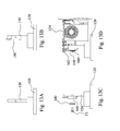
- Figs. 11A to 11D are sequential operation views of Fig. 10 .
- the sequence of steps of the sixth embodiment is according to the first embodiment, and the method for assembling the electronic device 100 includes the following steps.
- the step 1001 is welding the electronic component 160 on the printed wiring board 150 and providing the aforementioned heat-dissipating component 130.
- the step 1002 is covering the heat-dissipating component 130 with the printed wiring board 150, such that the electronic component 160 physically contacts the heat-dissipating component 130.
- the step 1003 is fixing the elastic clip 140 to the heat-dissipating component 130, so as to tightly clamp the electronic component 160 between the elastic clip 140 and the heat-dissipating component 130.
- the heat-dissipating component 130 is monolithically formed with the bottom case 120 (shown in Fig. 11A ), and the aforementioned electronic component 160 such as the transistor is welded on the printed wiring board 150 before the printed wiring board 150 covers the heat-dissipating component 130 (shown in Fig. 11 B) .
- the electronic component 160 of Fig. 11B is uprightly welded on the printed wiring board 150.
- the electronic component 160 may be flatly disposed on the printed wiring board 150.
- the printed wiring board 150 welded with the electronic component 160 of Fig.
- the elastic clip 140 of Fig. 11D physically contacts a surface away from the heat-dissipating component 130 of the electronic component 160, and the elastic clip 140 presses the electronic component 160 towards the heat-dissipating component 130 hard and fixes the electronic component 160 to the heat-dissipating component 130.
- the heat-dissipating component 130 and the electronic components 160 are disposed on a portion of the bottom board 122 of the bottom case 120 near the portion of the side wall with the smaller height (shown in Fig. 2 ), and if the fixing portion 142 of the elastic clip 140 may be exposed by the side wall 123, the position in which the elastic clip 140 is fixed to the heat-dissipating component 130 (that is, fixing portion) is not blocked by the side wall 123 of the bottom case 120(shown in Fig. 2 ), and assembly workers may easily fix the elastic clip 140 to the heat-dissipating component 130 from outside. Therefore, no additional special fixing tools are needed, and the assembling time and cost are reduced.
- the heat-dissipating component 130 is monolithically formed with the bottom case 120 (shown in Fig. 11A ), embodiments of this invention are not limited thereto. In other embodiments, such as the embodiment shown in Fig. 6A and Fig. 6B , if the aforementioned heat-dissipating component 230 is independent from the bottom case 120, a step of assembling the heat-dissipating component 230 to the bottom case 120 may be performed before the step 1002 or after the step 1003.
- Fig. 12 is a flowchart of the method for assembling the electronic device 100 in another sequence according to the sixth embodiment of this invention.
- Figs. 13A to 13D are sequential operation views of Fig. 12 .
- the sequence of the sixth embodiment is according to the first embodiment, and the method for assembling the electronic device 100 includes the following steps.
- Step 1201 is providing the aforementioned heat-dissipating component 130 and the aforementioned electronic component 160.
- Step 1202 is enabling the heat-dissipating component 130 physically contact the electronic component 160.
- Step 1203 is fixing the elastic clip 140 to the heat-dissipating component 130, so as to tightly clamp the electronic component 160 between the elastic clip 140 and the heat-dissipating component 130.
- Step 1204 is covering the electronic component 160 with the printed wiring board 150.
- Step 1205 is welding the electronic component 160 on the printed wiring board 150.
- the heat-dissipating component 130 is monolithically formed with the bottom case 120 (shown in Fig. 13A ), and the aforementioned electronic component 160 is still not mounted on the printed wiring board 150 (shown in Fig. 13B ).
- the electronic component 160 without welding contacts a surface of the heat-dissipating component 130 of Fig. 13B .
- the elastic clip 140 contacts a surface away from the heat-dissipating component 130 (shown in Fig. 13C ) of the electronic component 160, and the elastic clip 140 presses the electronic component 160 towards the heat-dissipating component 130 hard and fixes the electronic component 160 to the heat-dissipating component 130.
- the printed wiring board 150 is covered on the electronic component 160 (shown in Fig. 13D ), such that pin feet 162 of the electronic component 160 are inserted in the printed wiring board 150, so as to perform the welding process in the step 1205.
- the electronic component 160 is supported only by the pin feet 162. By welding the electronic component 160 to the printed wiring board 150 after the heat-dissipating component 130 and the elastic clip 140 are assembled to the electronic component 160, the entire structure of the electronic component 160 is strengthened, and the risk that the pin feet 162 are deformed due to the inhomogeneous pressure may be reduced.
- the heat-dissipating component 130 is monolithically formed with the bottom case 120 (shown in Fig. 11A ), however, embodiments of this invention are not limited thereto. In other embodiments, such as the embodiment shown in Fig. 6A and Fig. 6B , if the aforementioned heat-dissipating component 230 is independent from the bottom case 120, a step of assembling the heat-dissipating component 230 to the bottom case 120 is performed before the step 1202 or after the step 1203.
- Fig. 14 is a flowchart of a method for assembling the electronic device 101 according to a seventh embodiment of this invention.
- Figs. 15A to 15C are sequential operation views of Fig. 14 .
- the seventh embodiment is according to the third embodiment, and the method for assembling the electronic device 101 includes the following steps.
- Step 1401 is assembling the elastic clip 240 on the heat-dissipating component 230, thereby forming a clamping space 244 between the elastic clip 240 and the heat-dissipating component 230 (shown in Fig. 15A ).
- step 1402 is inserting the electronic component 160 into the clamping space 244, so as to clamp the electronic component 160 between the heat-dissipating component 230 and the elastic clip 240 (shown in Fig. 15B ).
- the step 1403 is assembling the heat-dissipating component 230 on the bottom case 120 (shown in Fig. 15C ).
- the assembling time may become shorter, and the assembling process for the electronic component 160 may become more flexible.
- step 1401 the elastic clip 240 and the heat-dissipating component 230 of Fig. 15A are moved towards the electronic component 160, such that the electronic component is inserted in the clamping space 244 and that the electronic component 160 is clamped between the heat-dissipating component 230 and the elastic clip 240.
- step 1403 the step of assembling the heat-dissipating component 230 of Fig. 15C on the bottom case 120 is performed after the elastic clip 240 is assembled to the heat-dissipating component 230 (shown in Fig. 15A ).
- the method includes welding the electronic component 160 on the printed wiring board 150.
- the step of welding the electronic component 160 to the printed wiring board 150 may be performed before or after the elastic clip 240 is assembled to the heat-dissipating component 230.
- the seventh embodiment is not limited to the aforementioned description.
- the step of assembling the heat-dissipating component 230 to the bottom case 120 described in step 1403 may be performed before step 1401.
- step 1403 that is, assembling the heat-dissipating component to the bottom case, need not to be performed.
Landscapes
- Engineering & Computer Science (AREA)
- Microelectronics & Electronic Packaging (AREA)
- Physics & Mathematics (AREA)
- Thermal Sciences (AREA)
- Power Engineering (AREA)
- Manufacturing & Machinery (AREA)
- Transportation (AREA)
- Mechanical Engineering (AREA)
- Cooling Or The Like Of Electrical Apparatus (AREA)
- Cooling Or The Like Of Semiconductors Or Solid State Devices (AREA)
- Dc-Dc Converters (AREA)
- Electric Propulsion And Braking For Vehicles (AREA)
- Shielding Devices Or Components To Electric Or Magnetic Fields (AREA)
Abstract
Description
- A hybrid electric vehicle or an electric vehicle has the advantages of economy, energy saving and environmental protection, etc., and has become the main focus of research and development for the major automobile companies under the crisis of energy shortage. With the advance of the automobile industry, vehicle amount has been increasing, and the pressure from the environmental pollution and the energy shortage has become obvious. At present, as the world is running out of fossil fuel, and the situation of global warming is getting urgent, countries around the world regard energy saving and environmental protection as the prior direction of development for the future automobile industry. With their obvious features of high efficiency, energy saving, low noise and null emission, electric vehicles have an incomparable superiority in the aspect of energy saving and environmental protection. In recent years, the electric vehicles have achieved great improvements in the core technologies such as power battery, electrical motor, control system, and on board charger module. The safety, reliability, and lifetime of products are significantly raised, and the manufacturing cost is under a certain level of control. Hybrid electric vehicles and electric vehicles are gradually entering the stage of practical use and small industrialization, and will be the strategic direction of the development of the automobile industry.
- As one of the key components of electric vehicle, a charger module can be classified as an off board charger module and an on board charger module (OBCM). The off board charger module, which is also referred to as a ground charging device or a charging pile, often has a larger power, larger volume, and greater mass. The OBCM is a device mounted on an electric vehicle for charging a battery pack by the AC power grid, in which an AC power cable is plugged into a socket of the electric vehicle to get it charged. The OBCM is essentially a power conversion device. The OBCM uses input wires to receive alternative current which is coupled to AC power grid, and outputs high voltage direct current to charge the on board high voltage battery pack, and uses a communication port to maintain real-time interactive communications with a battery management system (BMS). The overall performance enhancement and the cost control of the OBCM are always key factors restricting the mass production of electric vehicles, and the structure design and the thermal management of the OBCM are ones of the most critical indicators for comprehensively evaluating the performance of the OBCM.
- However, the OBCM, or the power conversion device, consumes a lot of electricity, the electronic components in the power conversion device generate quite a lot of heat with the increasing of power density of the OBCM or device, and if the electronic components do not physically contact the heat spreaders, the heat-dissipating efficiency is limited and the heat transferring performance is not good.
- In view of the foregoing, there still exist inconvenience and defects in the aforementioned conventional hardware configuration, and further improvements need to be made. In order to solve the above problems, those who are in related fields have made a lot of efforts, but suitable solutions have not been developed. Therefore, how to enhance the heat-dissipating efficiency is becoming an important R&D topic, and is a goal that urgently needs to be improved.
- This disclosure provides an electronic device and a method for assembling the same.
- In one embodiment, an electronic device is provided. The electronic device includes a bottom case, an accommodation unit, an electromagnetic induction module, a heat-dissipating component, an elastic clip, a printed wiring board, and an electronic component. The accommodation unit is disposed on the bottom case. At least one portion of the electromagnetic induction module is disposed in the accommodation unit. The heat-dissipating component is disposed on the bottom case and is positioned separately from the accommodation unit. The elastic clip is partially mounted on the heat-dissipating component. The printed wiring board has a first surface and a second surface, and the first surface faces the accommodation unit. The electronic component includes a main body and a plurality of pin feet. The pin feet are electrically connected to the printed wiring board, and the main body is clamped between the heat-dissipating component and the elastic clip.
- In another embodiment, a method for assembling an electronic device is provided. The method includes enabling a heat-dissipating component to physically contact an electronic component, and fixing an elastic clip to the heat-dissipating component, so as to clamp the electronic component between the heat-dissipating component and the elastic clip.
- In another embodiment, a method for assembling an electronic device is provided. The method includes assembling an elastic clip on a heat-dissipating component, thereby forming a clamping space between the elastic clip and the heat-dissipating component, and inserting an electronic component into the clamping space, so as to clamp the electronic component between the heat-dissipating component and the elastic clip.
- The electronic device and the method for assembling the electronic device provided by the disclosure may be applied to all electronic devices or to the relevant technical aspects such as vehicle charger modules. Whenever the electronic component is uprightly disposed or is flatly disposed, the heat-dissipating efficiency of the electronic component may be enhanced by the configurations of this invention. Therefore, the failure risk of the electronic component due to the overheating may be reduced, and the life of the electronic component may be increased.
- In sum, compared to the prior art, the aforementioned embodiments may have the following characteristics:
- 1. the assembling time becomes shorter;
- 2. the method for assembling the electronic component becomes more flexible; and
- 3. the heat-dissipating efficiency of the electronic component is enhanced.
- It is to be understood that both the foregoing general description and the following detailed description are by examples, and are intended to provide further explanation of the invention as claimed.
- The invention can be more fully understood by reading the following detailed description of the embodiment, with reference made to the accompanying drawings as follows:
-
Fig. 1 is an assembled view of an electronic device according to a first embodiment of this invention; -
Fig. 2 is a partially exploded view ofFig. 1 ; -
Fig. 3 is an exploded view showing a bottom case and a printed wiring board ofFig. 2 ; -
Fig. 4 is a partially enlarged view of an area M ofFig. 2 ; -
Fig 5A is a 3-D view of an insulated strut according to a second embodiment of this invention; -
Fig. 5B is an exploded cross-sectional view of the printed wiring board, the insulated strut, and a heat-dissipating component according to the second embodiment of this invention; -
Fig. 6A is an exploded view of an electronic device according to a third embodiment of this invention; -
Fig. 6B is an assembled view of an elastic clip and a heat-dissipating component according to the third embodiment of this invention; -
Fig. 7A is a top view of a bottom case according to a fourth embodiment of this invention; -
Fig. 7B is a cross-sectional view viewed along line A-A ofFig. 7A ; -
Fig. 8 is a top view of a bottom case according to a fifth embodiment of this invention; -
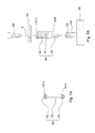
Fig. 9 is a flowchart of a method for assembling an electronic device according to a sixth embodiment of this invention; -
Fig. 10 is a flowchart of the method for assembling the electronic device in one sequence according to the sixth embodiment of this invention; -
Figs. 11A to 11D are sequential operation views ofFig. 10 ; -
Fig. 12 is a flowchart of the method for assembling the electronic device in another sequence according to the sixth embodiment of this invention; -
Figs. 13A to 13D are sequential operation views ofFig. 12 ; -
Fig. 14 is a flowchart of a method for assembling an electronic device according to a seventh embodiment of this invention; and -
Figs 15A to 15C are sequential operation views ofFig. 14 . - In the following detailed description, for purposes of explanation, numerous specific details are set forth in order to provide a thorough understanding of the disclosed embodiments. It will be apparent, however, that one or more embodiments may be practiced without these specific details. In other words, these specific details are not essential to practice one or more embodiments. Besides, well-known structures and devices are schematically depicted in order to simplify the drawings.
- The terminology used herein is for the purpose of describing particular embodiments only and is not intended to be limiting of the invention. As used herein, the singular forms "a", "an" and "the" are intended to include the plural forms as well, unless the context clearly indicates otherwise.
- As used herein, "around", "about" or "approximately" shall generally mean within 20 percent, preferably within 10 percent, and more preferably within 5 percent of a given value or range. Numerical quantities given herein are approximate, meaning that the term "around", "about" or "approximately" can be inferred if not expressly stated.
-
Fig. 1 is an assembled view of anelectronic device 100 according to a first embodiment of this invention.Fig. 2 is a partially exploded view ofFig. 1 . As shown inFig. 1 andFig. 2 , anelectronic device 100 is provided. Theelectronic device 100 includes abottom case 120, a heat-dissipatingcomponent 130, anelastic clip 140, a printedwiring board 150, and at least oneelectronic component 160 such as a transistor. The heat-dissipatingcomponent 130 is disposed on thebottom case 120. Theelastic clip 140 is partially mounted on the heat-dissipatingcomponent 130. Each of theelectronic components 160 includes amain body 161 andpin feet 162. Thepin feet 162 are electrically connected to the printedwiring board 150, and themain body 161 is clamped between the heat-dissipatingcomponent 130 and theelastic clip 140. - In the above deposition configuration, the heat-dissipating
component 130 and theelectronic component 160 tightly contact each other through theelastic clip 140. Therefore, no matter how theelectronic component 160 is disposed, the failure risk of theelectronic component 160 due to the overheating may be reduced, and the lifetime of theelectronic component 160 may be increased. -
Fig. 3 is an exploded view showing thebottom case 120 and the printedwiring board 150 ofFig. 2 . As shown inFig. 2 andFig. 3 , thebottom case 120 includes anaccommodation unit 170 and anelectromagnetic induction module 171. Theaccommodation unit 170 is disposed on thebottom case 120 and may be positioned separately from the heat-dissipatingcomponent 130. At least one portion of theelectromagnetic induction module 171 is disposed in theaccommodation unit 170, and the other portion of theelectromagnetic induction module 171 is disposed outside theaccommodation unit 170. In other embodiments, the entire electromagnetic induction module may be disposed in the accommodation unit. - Because the
electromagnetic induction module 171 generates a lot of heat when operating, the heat generated by theelectromagnetic induction module 171 may be dissipated to thebottom case 120 by theaccommodation unit 170. At this time, because the heat-dissipatingcomponent 130 is positioned separately from theaccommodation unit 170, the heat generated by theelectromagnetic module 171 may be prevented from directly transferring to the heat-dissipatingcomponent 130, thus maybe avoiding affecting the heat-dissipating efficiency of the heat-dissipatingcomponent 130 for theelectronic component 160. - As shown in
Fig. 2 andFig. 3 , specifically, electronic parts, such as transistors, capacitors, etc., are disposed on the printedwiring board 150. The printedwiring board 150 has afirst surface 151 and asecond surface 152. The printedwiring board 150 is fixed to the portion of theelectromagnetic induction module 171 outside theaccommodation unit 170 by screws T1, such that thefirst surface 151 faces theaccommodation unit 170 and thebottom case 120. Therefore, the screws not only fix the printedwiring board 150 to theelectromagnetic induction module 171 but also electrically couple the printedwiring board 150 to theelectromagnetic induction module 171. - In addition, the
electronic components 160 are disposed on the printed wiring board. Specifically, theelectronic components 160 are uprightly disposed on thefirst surface 151 of the printedwiring board 150. Because theelectronic components 160 are respectively uprightly disposed on the printedwiring board 150 and are respectively tightly clamped between the heat-dissipatingcomponent 130 and theelastic clip 140, areas on the printedwiring board 150 occupied by theelectronic component 160 may become smaller to reduce the volume of theelectronic device 100, and the heat may be effectively dissipated due to a high thermal conductivity of the heat-dissipatingcomponent 130. Because the surfaces with the maximum areas at the same side of theelectronic components 160 are aligned to each other, the surfaces at the same side of theelectronic component 160 contact the heat-dissipatingcomponent 130 to provide better heat-dissipating performance. Embodiments of this invention are not limited thereto. In other embodiments, the electronic components may be flatly disposed on the first surface of the printed wiring board, such that the electronic component may be tightly clamped between the heat-dissipating component and the elastic clip easily. - Additionally, each of the
main bodies 161 is clamped between the heat-dissipatingcomponent 130 and the elastic clip 140 (shown inFig. 2 ). Each of thepin feet 162 is disposed between the main body and the printedwiring board 150, and is electrically connected to the printedwiring board 150 and themain body 161. An appropriate distance L is maintained between themain body 161 and the printedwiring board 150, and themain body 161 is spaced from the printedwiring board 150 at the distance L. -
Fig. 4 is a partially enlarged view of an area M ofFig. 2 . As shown inFig. 4 , in the first embodiment, theelastic clip 140 includes amain body 141, a fixingportion 142 and apressing portion 143. The fixingportion 142 is located on a portion of themain body 141, and is mounted on the heat-dissipatingcomponent 130 by fixing components such as screws T3. Thepressing portion 143 is located on another portion of themain body 141 and presses theelectronic component 160 to contact the heat-dissipatingcomponent 130. For example, themain body 141 may be a stripe, and theelastic clip 140 may include twopressing portions 143. The twopressing portions 143 are disposed on two opposite ends of themain body 141. Each of the twopressing portions 143 is convex. The fixingportion 142 is located between the twopressing portions 143 and is fixed to the heat-dissipatingcomponent 130 by the screws T3 disposed in a gap between any twoadjacent bodies 161. - Therefore, the fixing
portion 142 is fixed to the heat-dissipatingcomponent 130 in a direction from theelastic clip 140 to the heat-dissipatingcomponent 130 by the screws T3, and themain body 141 of theelastic clip 140 is forced to respectively push the twopressing portions 143 in a direction D1 towards the heat-dissipatingcomponent 130, such that a surface of themain body 161 tightly contacts a surface of the heat-dissipatingcomponent 130, thereby maybe generating sufficient contact pressure on a contact surface between themain body 161 and the heat-dissipatingcomponent 130, and meanwhile maybe eliminating the gap between themain body 161 and the heat-dissipating 130, thus lowering an interfacial thermal resistance between themain body 161 and the heat-dissipatingcomponent 130. - The disclosure does not intend to limit the materials of the heat-dissipating
component 130 and theelastic clip 140. However, when the materials of the heat-dissipatingcomponent 130 and theelastic clip 140 are conductive materials such as metals, the surfaces of the heat-dissipatingcomponent 130 and theelastic clip 140 are covered with thermal conductive isolation layers (not shown in Figures) so as to be electrically isolated fromelectronic components 160. - As shown in
Fig. 3 andFig. 4 , thebottom case 120 is a cold plate base which is hollow, and a fluid passage is disposed in thebottom case 120. By injecting a liquid passing through the fluid passage, the heat-dissipating efficiency may be enhanced. In addition, as shown inFig. 2 , in the embodiment, theelectronic device 100 further includes atop cover 110. Thetop cover 110 covers thebottom case 120, and thetop cover 110 is fixed to thebottom case 120 by screws T2, such that all of the aforementioned components are disposed between thetop cover 110 and thebottom case 120 and are protected. In order to enhance the heat-dissipating efficiency, thetop cover 110 may further havefins 111. - As shown in
Fig. 3 , thebottom case 120 includes abottom board 122 andside walls 123. Theside walls 123 surround and are connected to thebottom board 122, and extend towards the printedwiring board 150, such that anaccommodation space 124 is defined. Theaccommodation space 124 accommodates the heat-dissipatingcomponent 130, theelastic clip 140, theaccommodation unit 170, theelectromagnetic induction module 171, the printedwiring board 150 and theelectronic component 160. Theaccommodation unit 170 is disposed on thebottom board 122 and between the printedwiring board 150 and thebottom board 122. The printedwiring board 150 is fixed to theelectromagnetic induction module 171 by fixing members such as the screws T1. The heat-dissipatingcomponent 130 faces aninner surface 123A of one of theside walls 123. In the first embodiment, the heat-dissipatingcomponent 130 is monolithically formed with thebottom board 122 of thebottom case 120. An adequate distance F is maintained between the heat-dissipatingcomponent 130 and aninner surface 123A of the one of theside walls 123 disposed in thebottom case 120. - People having ordinary skills in the art can make proper modifications to the heat-dissipating
component 130 and thebottom case 120 according to their actual applications. In other embodiments, the heat-dissipating component may be dismantably mounted on the bottom board of the bottom case. - In the first embodiment, the
elastic clip 140 is closer to theside wall 123 facing the heat-dissipatingcomponent 130 than the heat-dissipatingcomponent 130 is. Anouter surface 123B of theside wall 123 is a portion of the outer surface of theelectronic device 100. A height H1 of theside wall 123, i.e., a minimum distance between a top surface of theside wall 123 away from thebottom board 122 and thebottom board 122, is smaller than a height H2, i.e., a minimum distance between the fixingportion 142 and thebottom board 122. In other words, as shown inFig. 2 andFig. 3 , after the printedwiring board 150 is assembled on thebottom case 120, theside wall 123 of thebottom case 120 is not too high and thus does not block the fixingportion 142 of theelastic clip 140. For example, a height of theside wall 123 on the left side is smaller from the one end of theside wall 123 to the other end of theside wall 123, such that a height H3 of theside wall 123 is reduced to a height H4, and the fixingportion 142 ofelastic clip 140 is exposed from a portion of theside wall 123 with a smaller height. - Therefore, in the first embodiment, because the
elastic clip 140 is closer to theside wall 123 facing the heat-dissipatingcomponent 130 than the heat-dissipatingcomponent 130 is, and because the fixingportion 142 ofelastic clip 140 is exposed from the portion of theside wall 123 with a smaller height, theelastic clip 140 can be easily fixed to the heat-dissipatingcomponent 130 by assembly workers from a position near the portion of theside wall 123 with a smaller height, and theelastic clip 140 may be fixed to the heat-dissipatingcomponent 130 after the printedwiring board 150 covers theelectromagnetic induction module 171. Therefore, the assembling time becomes shorter, and the assembling process becomes more flexible, and no other additional special fixing tools are needed, thus reducing the assembling time and cost. -
Fig 5A is a 3-D view of aninsulated strut 180 according to a second embodiment of this invention.Fig. 5B is an exploded cross-sectional view of the printedwiring board 150, theinsulated strut 180, and the heat-dissipatingcomponent 130 according to the second embodiment of this invention. Theinsulated strut 180 may be applied in the first embodiment. As shown inFig. 5B , in order to fix and electrically insulate the printedwiring board 150 and thebottom case 120, at least oneinsulated strut 180 is disposed between thewiring 150 and thebottom case 120. Theinsulated strut 180 is connected to the heat-dissipatingcomponent 130 and the printedwiring board 150, and theinsulated strut 180 physically fixes and electrically insulates the heat-dissipatingcomponent 130 from the printedwiring board 150. - Specifically, the
insulated strut 180 includes a first connectingpart 182, a second connectingpart 183, and aplastic part 181 partially covering the first connectingpart 182 and the second connectingpart 183. The first connectingpart 182 may be connected to the printedwiring board 150, and the first connectingpart 182 may be a nut. The second connectingpart 183 may be connected to thebottom case 120, and the second connectingpart 183 may be a stud. Therefore, the printedwiring board 150 and thebottom base 120 may be fixed through theinsulated strut 180. Theplastic part 181 includes afirst end surface 181A and asecond end surface 181B opposite to thefirst end surface 181A. The first connectingpart 182 is embedded in thefirst end surface 181A. A portion of the second connectingpart 183 is disposed in theplastic part 181, and the other portion of the second connecting part protrudes from thesecond end surface 181B. - More specifically, the first connecting
part 182 may be a nut, and the second connectingpart 183 may be a stud. The second connectingpart 183 is fixed to thebottom case 120, and the printedwiring board 150 is fixed to the first connectingpart 182 through ascrew 184. The first connectingpart 182 may be a blind-hole nut. The main body of the nut is substantially disposed in theplastic part 181, and only an upper surface of the nut is disposed outside theplastic part 181 to expose a screw hole P in the nut. The second connectingpart 183 is a stud, a head of the stud is disposed in theplastic part 181, and a threaded portion of the stud is disposed outside theplastic part 181 to correspond to ascrew hole 185 on thebottom case 120. - In order to effectively electrically insulate the printed
wiring board 150 frombottom case 120, the first connectingpart 182 and the second connectingpart 183 are positioned separately by theplastic part 181. Though the first connectingpart 182 and the second connectingpart 183 are both metals, theplastic part 181 is disposed between the first connectingpart 182 and the second connectingpart 183, such that the first connectingpart 182 may not directly contact the second connectingpart 183 and an adequate safety distance is maintained. -
Fig. 6A is an exploded view of anelectronic device 101 according to a third embodiment of this invention.Fig. 6B is an assembled view of theelastic clip 240 and the heat-dissipatingcomponent 230 according to the third embodiment of this invention. As shown inFig. 6A , theelectronic device 101 of the third embodiment is similar to theelectronic device 100 of the first embodiment, and the only difference is that the appearances of theelastic clip 240 and the heat-dissipatingcomponent 230 of the third embodiment are different from the appearances of theelastic clip 140 and the heat-dissipatingcomponent 130 of the first embodiment. Specifically, the heat-dissipatingcomponent 230 is an independent object, and the heat-dissipatingcomponent 230 is dismantably mounted on thebottom case 120. The heat-dissipatingcomponent 230 includes a heat-dissipatingblock 231 and abase 232. The heat-dissipatingblock 231 partially contacts theelectronic component 160. Thebase 232 is connected to thebottom case 120. For example, thebase 232 is a strip. One side of thebase 232 is connected to the heat-dissipatingblock 231, and two opposite ends of the base 232 are fixed to thebottom case 120 through screws T4. Though there is no printed wiring board inFig. 6B , it only means that theelectronic component 160 is not mounted on thebottom case 120 yet, and it does not mean that theelectronic component 160 does not need to be mounted on the printed wiring board. The heat-dissipatingcomponent 230 may be assembled on thebottom case 120 before or after contacting theelectronic component 160. - Therefore, the deposition position of heat-dissipating
component 230 may be adjusted according to the deposition position of theelectronic component 160. Then, as long as the heat-dissipatingcomponent 230 is fixed to thebottom case 120, the heat-dissipatingcomponent 230 provides theelectronic component 160 with an appropriate heat-dissipating path. - Additionally, as shown in
Fig. 6A andFig. 6B , in the third embodiment, theelastic clip 240 includes amain body 241, a fixingportion 242 and apressing portion 243. For example, themain body 241 is a stripe. Three fixingportions 242 are disposed on themain body 241 at intervals, and the fixingportions 242 is fixed to the base 232 through the screws T3, such that a clampingspace 244 allowing themain body 161 to inserted therein is formed between theelastic clip 240 and the heat-dissipatingblock 231. The threepressing portions 243 all extend outwardly from one side of themain body 241. The number of thepressing portions 243 is the same as the number of thebodies 161, and thepressing portions 243 are respectively corresponding to thebodies 161. Each of thepressing portions 243 is hook-shaped, and one end of each of thepressing portions 243 presses the correspondingmain body 161 towards the direction D1. - By designing each of the
pressing portions 243 bending towards the heat-dissipatingblock 231, each of thepressing portion 243 are forced to press themain body 161 towards the heat-dissipatingblock 231, such that one surface of themain body 161 tightly contact one surface of the heat-dissipatingblock 231. Therefore, adequate contact pressure on the contact surface of themain body 161 and the heat-dissipatingblock 231 is generated, and a gap between themain body 161 and the heat-dissipatingblock 231 is eliminated, such that an interfacial thermal resistance between themain body 161 and the heat-dissipatingblock 231 is lowered. - The disclosure does not intend to limit the materials of the heat-dissipating
component 230 and theelastic clip 240. However, when the materials of the heat-dissipatingcomponent 230 and theelastic clip 240 are conductive materials such as metals, an isolation layer with a high thermal conductivity (not shown in Figures) covers surfaces of the heat-dissipatingcomponent 230 and theelastic clip 240 to electrically isolateelectronic components 160. -
Fig. 7A is a top view of thebottom case 120 according to a fourth embodiment of this invention.Fig. 7B is a cross-sectional view viewed along line A-A ofFig. 7A . As shown inFig. 7A , the difference between the first embodiment and the fourth embodiment is that the printedwiring board 250 is disposed on thebottom board 122 of thebottom case 120, the printedwiring board 250 and theaccommodation unit 170 are disposed side by side, and the printedwiring board 250 is not disposed on theelectromagnetic induction module 171. Theelectronic components 260 are flatly disposed on the printedwiring board 250. Specifically, theelectronic components 260 such as transistors are flatly disposed on one surface away from thebottom board 122 of the printedwiring board 250. Embodiments of this invention are not limited thereto. In other embodiments, the electronic component is uprightly disposed on a surface away from the bottom case of the printed wiring board, such that the electronic component may be easy to be tightly clamped between the heat-dissipating component and the elastic clip. - In addition, each of the
electronic components 260 includes amain body 261 andpin feet 262. One end of each of thepin feet 262 is electrically connected to the printedwiring board 250, and the other end of each of thepin feet 262 supports themain body 261 after bending. As shown inFig. 7B , each of thebodies 261 is clamped between the heat-dissipatingcomponent 330 and theelastic clip 140. - The disclosure does not intend to limit the materials of the heat-dissipating
component 330 and theelastic clip 140. However, when the materials of the heat-dissipatingcomponent 330 and theelastic clip 140 are conductive materials such as metals, an isolation layer with a high thermal conductivity (not shown in Figures) covers surfaces of the heat-dissipatingcomponent 330 and theelastic clip 140 to electrically isolateelectronic components 260. - Additionally, as shown in
Fig. 7A andFig. 7B , a side surface of the heat-dissipatingcomponent 330 is connected to one of theside walls 123 of thebottom case 120, and the heat-dissipatingcomponent 330 is monolithically formed with thebottom board 122. Theelastic clip 140 is mounted on the heat-dissipatingcomponent 330 through the fixing component such as the screws T3. Therefore, the heat-dissipatingcomponent 330 dissipates heat to thebottom case 120 through two paths, and the heat-dissipating efficiency of the heat-dissipatingcomponent 330 is enhanced. - People having ordinary skill in the art can make proper modification to the heat-dissipating
component 330 and thebottom case 120 according to their actual applications. In other embodiments, the heat-dissipating component may be dismantably mounted on the bottom case. -
Fig. 8 is a top view of thebottom case 120 according to a fifth embodiment of this invention. As shown inFig. 8 , the difference between the fourth embodiment and the fifth embodiments is that the form of theelastic clip 240 of the fifth embodiment is different from theelastic clip 140 ofFig. 7A . - As shown in
Fig. 8 , the heat-dissipatingcomponent 330 is a heat-dissipating block monolithically formed with thebottom board 122 of thebottom case 120. For clearly illustrating the connection relation between the heat-dissipation component 330 and thebottom board 122 of thebottom case 120, oneelectronic component 160 corresponding to the leftmostpressing portion 243 is omitted. The number ofelectronic components 160 shown inFig. 8 is three, which does not mean the actual number of theelectronic component 160 of the fifth embodiment. Theelastic clip 240 includes amain body 241, two fixingportions 242, andpressing portions 243. Themain body 241 is a strip. The two fixingportions 242 are disposed on themain body 241 at intervals, and the fixingportions 242 are fixed to the heat-dissipatingcomponent 330 through the screws T3. Thepressing portions 243 all extend outwardly from one side of themain body 241. A number of thepressing portions 243 is the same as a number of thebodies 161, and thepressing portions 243 respectively correspond to thebodies 161. Each of thepressing portions 243 is hook-shaped, and one end of each of thepressing portion 243 presses the correspondingmain body 161. - By designing each of the
pressing portions 243 bending towards the heat-dissipatingcomponent 330, each of thepressing portion 243 presses themain body 161 towards the heat-dissipatingcomponent 330, such that one surface of themain body 161 tightly contact one surface of the heat-dissipatingcomponent 330. Therefore, a contact surface between themain body 161 and the heat-dissipatingcomponent 330 is increased, and a gap between themain body 161 and the heat-dissipatingcomponent 330 is eliminated. Because each of the surfaces with the maximum areas of theelectronic components 160 are aligned to each other, the surfaces at the same side of theelectronic components 160 contact the heat-dissipatingcomponent 330, and a better heat-dissipating efficiency is provided. -
Fig. 9 is a flowchart of a method for assembling the electronic device according to a sixth embodiment of this invention. As shown inFig. 3 andFig. 9 , a method for assembling an electronic device is provided. The method includes the following steps. Step 901 is enabling the heat-dissipatingcomponent 130 to physically contact theelectronic component 160. Then, step 902 is fixing theelastic clip 140 to the heat-dissipatingcomponent 130, so as to clamp theelectronic component 160 between the heat-dissipatingcomponent 130 and theelastic clip 140. Before or after welding theelectronic component 160 on the printedwiring board 150, theelectronic component 160 is fixed to the heat-dissipatingcomponent 130 through theelastic clip 140, such that two opposite sides of the electronic component160 respectively tightly contact theelastic clip 140 and the heat-dissipatingcomponent 130. Therefore, the assembling time may become shorter, and the assembling process for theelectronic component 160 may become more flexible. - Though the heat-dissipating
component 130 is monolithically formed with the bottom case 120 (shown inFig. 3 ) in the method, embodiments of this invention are not limited thereto. In other embodiments, such as the embodiment shown inFig. 6A andFig. 6B , if the aforementioned heat-dissipatingcomponent 230 is independent from thebottom case 120, a step of assembling the heat-dissipatingcomponent 230 to thebottom case 120 is performed before thestep 901 or after thestep 902. -
Fig. 10 is a flowchart of the method for assembling theelectronic device 100 in one sequence according to the sixth embodiment of this invention.Figs. 11A to 11D are sequential operation views ofFig. 10 . As shown inFig. 10 andFigs. 11A to 11D , the sequence of steps of the sixth embodiment is according to the first embodiment, and the method for assembling theelectronic device 100 includes the following steps. - The
step 1001 is welding theelectronic component 160 on the printedwiring board 150 and providing the aforementioned heat-dissipatingcomponent 130. Thestep 1002 is covering the heat-dissipatingcomponent 130 with the printedwiring board 150, such that theelectronic component 160 physically contacts the heat-dissipatingcomponent 130. Thestep 1003 is fixing theelastic clip 140 to the heat-dissipatingcomponent 130, so as to tightly clamp theelectronic component 160 between theelastic clip 140 and the heat-dissipatingcomponent 130. - Specifically, in the
step 1001, the heat-dissipatingcomponent 130 is monolithically formed with the bottom case 120 (shown inFig. 11A ), and the aforementionedelectronic component 160 such as the transistor is welded on the printedwiring board 150 before the printedwiring board 150 covers the heat-dissipating component 130 (shown inFig. 11 B) . In the embodiment, theelectronic component 160 ofFig. 11B is uprightly welded on the printedwiring board 150. However, theelectronic component 160 may be flatly disposed on the printedwiring board 150. In thestep 1002, the printedwiring board 150 welded with theelectronic component 160 ofFig. 11C is covered on the heat-dissipatingcomponent 130, such that a surface of the heat-dissipatingcomponent 130 contacts a common mounting surface of theelectronic components 160. In thestep 1003, theelastic clip 140 ofFig. 11D physically contacts a surface away from the heat-dissipatingcomponent 130 of theelectronic component 160, and theelastic clip 140 presses theelectronic component 160 towards the heat-dissipatingcomponent 130 hard and fixes theelectronic component 160 to the heat-dissipatingcomponent 130. - As described in the first embodiment, if the heat-dissipating
component 130 and theelectronic components 160 are disposed on a portion of thebottom board 122 of thebottom case 120 near the portion of the side wall with the smaller height (shown inFig. 2 ), and if the fixingportion 142 of theelastic clip 140 may be exposed by theside wall 123, the position in which theelastic clip 140 is fixed to the heat-dissipating component 130 (that is, fixing portion) is not blocked by theside wall 123 of the bottom case 120(shown inFig. 2 ), and assembly workers may easily fix theelastic clip 140 to the heat-dissipatingcomponent 130 from outside. Therefore, no additional special fixing tools are needed, and the assembling time and cost are reduced. - Though in the sequence, the heat-dissipating
component 130 is monolithically formed with the bottom case 120 (shown inFig. 11A ), embodiments of this invention are not limited thereto. In other embodiments, such as the embodiment shown inFig. 6A andFig. 6B , if the aforementioned heat-dissipatingcomponent 230 is independent from thebottom case 120, a step of assembling the heat-dissipatingcomponent 230 to thebottom case 120 may be performed before thestep 1002 or after thestep 1003. -
Fig. 12 is a flowchart of the method for assembling theelectronic device 100 in another sequence according to the sixth embodiment of this invention.Figs. 13A to 13D are sequential operation views ofFig. 12 . As shown inFig. 12 andFigs. 13A to 13D , the sequence of the sixth embodiment is according to the first embodiment, and the method for assembling theelectronic device 100 includes the following steps.Step 1201 is providing the aforementioned heat-dissipatingcomponent 130 and the aforementionedelectronic component 160.Step 1202 is enabling the heat-dissipatingcomponent 130 physically contact theelectronic component 160.Step 1203 is fixing theelastic clip 140 to the heat-dissipatingcomponent 130, so as to tightly clamp theelectronic component 160 between theelastic clip 140 and the heat-dissipatingcomponent 130.Step 1204 is covering theelectronic component 160 with the printedwiring board 150.Step 1205 is welding theelectronic component 160 on the printedwiring board 150. - Specifically, in the
step 1201, the heat-dissipatingcomponent 130 is monolithically formed with the bottom case 120 (shown inFig. 13A ), and the aforementionedelectronic component 160 is still not mounted on the printed wiring board 150 (shown inFig. 13B ). In thestep 1202, theelectronic component 160 without welding contacts a surface of the heat-dissipatingcomponent 130 ofFig. 13B . In thestep 1203, theelastic clip 140 contacts a surface away from the heat-dissipating component 130 (shown inFig. 13C ) of theelectronic component 160, and theelastic clip 140 presses theelectronic component 160 towards the heat-dissipatingcomponent 130 hard and fixes theelectronic component 160 to the heat-dissipatingcomponent 130. In thestep 1204, the printedwiring board 150 is covered on the electronic component 160 (shown inFig. 13D ), such thatpin feet 162 of theelectronic component 160 are inserted in the printedwiring board 150, so as to perform the welding process in thestep 1205. - The
electronic component 160 is supported only by thepin feet 162. By welding theelectronic component 160 to the printedwiring board 150 after the heat-dissipatingcomponent 130 and theelastic clip 140 are assembled to theelectronic component 160, the entire structure of theelectronic component 160 is strengthened, and the risk that thepin feet 162 are deformed due to the inhomogeneous pressure may be reduced. - Though in the sequence, the heat-dissipating
component 130 is monolithically formed with the bottom case 120 (shown inFig. 11A ), however, embodiments of this invention are not limited thereto. In other embodiments, such as the embodiment shown inFig. 6A andFig. 6B , if the aforementioned heat-dissipatingcomponent 230 is independent from thebottom case 120, a step of assembling the heat-dissipatingcomponent 230 to thebottom case 120 is performed before thestep 1202 or after thestep 1203. -
Fig. 14 is a flowchart of a method for assembling theelectronic device 101 according to a seventh embodiment of this invention.Figs. 15A to 15C are sequential operation views ofFig. 14 . As shown inFig. 14 andFigs. 15A to 15C , the seventh embodiment is according to the third embodiment, and the method for assembling theelectronic device 101 includes the following steps. -
Step 1401 is assembling theelastic clip 240 on the heat-dissipatingcomponent 230, thereby forming a clampingspace 244 between theelastic clip 240 and the heat-dissipating component 230 (shown inFig. 15A ). Then,step 1402 is inserting theelectronic component 160 into the clampingspace 244, so as to clamp theelectronic component 160 between the heat-dissipatingcomponent 230 and the elastic clip 240 (shown inFig. 15B ). Then, thestep 1403 is assembling the heat-dissipatingcomponent 230 on the bottom case 120 (shown inFig. 15C ). Therefore, after or before theelectronic component 160 is welded to the printedwiring board 150, by inserting theelectronic component 160 into the clampingspace 244 between theelastic clip 240 and the heat-dissipatingcomponent 230, the assembling time may become shorter, and the assembling process for theelectronic component 160 may become more flexible. - Specifically, in
step 1401, theelastic clip 240 and the heat-dissipatingcomponent 230 ofFig. 15A are moved towards theelectronic component 160, such that the electronic component is inserted in the clampingspace 244 and that theelectronic component 160 is clamped between the heat-dissipatingcomponent 230 and theelastic clip 240. Instep 1403, the step of assembling the heat-dissipatingcomponent 230 ofFig. 15C on thebottom case 120 is performed after theelastic clip 240 is assembled to the heat-dissipating component 230 (shown inFig. 15A ). - As shown in
Fig. 15A , beforestep 1402, the method includes welding theelectronic component 160 on the printedwiring board 150. The step of welding theelectronic component 160 to the printedwiring board 150 may be performed before or after theelastic clip 240 is assembled to the heat-dissipatingcomponent 230. - The seventh embodiment is not limited to the aforementioned description. The step of assembling the heat-dissipating
component 230 to thebottom case 120 described instep 1403 may be performed beforestep 1401. - Though the heat-dissipating
component 230 is dismantably mounted on thebottom case 120 in the method, embodiments of this invention are not limited thereto. As shown inFig. 3 , if the heat-dissipatingcomponent 130 is monolithically formed with thebottom case 120,step 1403, that is, assembling the heat-dissipating component to the bottom case, need not to be performed.
Claims (15)
- An electronic device (100, 101), comprising:a bottom case (120);an accommodation unit (170) disposed on the bottom case (120);an electromagnetic induction module (171), wherein at least one portion of the electromagnetic induction module (171) is disposed in the accommodation unit (170);a heat-dissipating component (130, 230, 330) which is disposed on the bottom case (120) and positioned separately from the accommodation unit (170);an elastic clip (140, 240) partially mounted on the heat-dissipating component (130, 230, 330);a printed wiring board (150) having a first surface (151) and a second surface (152), wherein the first surface (151) faces the accommodation unit (170); andan electronic component (160, 260) comprising a main body (161, 261) and a plurality of pin feet (162, 262), wherein the pin feet (162, 262) are electrically connected to the printed wiring board (150), and the main body (161, 261) is clamped between the heat-dissipating component (130, 230, 330) and the elastic clip (140, 240).
- The electronic device (100, 101) of claim 1, wherein the electronic component (160) is uprightly or flatly disposed on the first surface (151) of the printed wiring board (150).
- The electronic device (101) of claim 1, wherein the heat-dissipating component (230) comprises:a heat-dissipating block (231) contacting the electronic component (160); anda base (232) which is connected to the heat-dissipating block (231) and mounted on the bottom case (120).
- The electronic device (100, 101) of claim 1, wherein the heat-dissipating component (130, 230, 330) is dismantably mounted on the bottom case (120) or monolithically formed with the bottom case (120).
- The electronic device (100, 101) of claim 1, wherein the elastic clip (140, 240) comprises:a main body (141, 241);a fixing portion (142, 242) which is disposed on the main body (141, 241) of the elastic clip (140, 240) and secured to the heat-dissipating component (130, 230, 330); anda pressing portion (143, 243) which is disposed on the main body (141, 241) of the elastic clip (140, 240) and presses the electronic component (160, 260) to contact the heat-dissipating component (130, 230, 330).
- The electronic device (100) of claim 5, wherein the bottom case (120) comprises:a bottom board (122) connected to the accommodation unit (170), wherein the accommodation unit (170) is disposed between the printed wiring board (150) and the bottom board (122); anda plurality of side walls (123) which are connected to and surround the bottom board (122), wherein the heat-dissipating component (130) faces an inner surface (123A) of one of the side walls (123);wherein a minimum straight distance (H1) between a top surface of the one of the side walls (123) located away from the bottom board (122) and the bottom board (122) is smaller than a minimum straight distance (H2) between the fixing portion (142) and the bottom board (122), and the elastic clip (140) is located nearer to the one of the side walls (123) facing the heat-dissipating component (130) than the heat-dissipating component (130) is.
- A method for assembling an electronic device (100, 101), comprising:enabling a heat-dissipating component (130, 230, 330) to physically contact an electronic component (160, 260); andfixing an elastic clip (140, 240) to the heat-dissipating component (130, 230, 330), so as to clamp the electronic component (100, 101) between the heat-dissipating component (130, 230, 330) and the elastic clip (140, 240).
- The method of claim 7, further comprising:welding the electronic component (160) on a printed wiring board (150) before or after the operation of fixing the elastic clip (140, 240) to the heat-dissipating component (130, 230).
- The method of claim 7, further comprising:assembling the heat-dissipating component (230) on a bottom case (120) after the elastic clip (240) is fixed to the heat-dissipating component (230) or before the operation of enabling the electronic component (160) to physically contact the heat-dissipating component (230).
- The method of claim 7, further comprising:covering the electronic component (160) with a printed wiring board (150) after the operation of fixing the elastic clip (140, 240) to the heat-dissipating component (130, 230); andwelding the electronic component (160) on the printed wiring board (150).
- The method of claim 7, further comprising:welding the electronic component (160) on a printed wiring board (150) before the operation of fixing the elastic clip (140, 240) to the heat-dissipating component (130, 230); andcovering the heat-dissipating component (130, 230) with the printed wiring board (150) welded with the electronic component (160).
- A method for assembling an electronic device (101), comprising:assembling an elastic clip (240) on a heat-dissipating component (230), thereby forming an clamping space (244) between the elastic clip (240) and the heat-dissipating component (230); andinserting an electronic component (160) into the clamping space (244), so as to clamp the electronic component (160) between the heat-dissipating component (230) and the elastic clip (240).
- The method of claim 12, further comprising:welding the electronic component (160) on a printed wiring board (150) after the operation of assembling the elastic clip (240) on the heat-dissipating component (230).
- The method of claim 12, further comprising:assembling the heat-dissipating component (230) on a bottom case (120) after the operation of assembling the elastic clip (240) on the heat-dissipating component (230).
- The method of claim 7 or 12, wherein the heat-dissipating component (130, 230, 330) is monolithically formed with a bottom case (120).
Applications Claiming Priority (1)
| Application Number | Priority Date | Filing Date | Title |
|---|---|---|---|
| CN201310612832.4A CN104684337B (en) | 2013-11-26 | 2013-11-26 | Electronic installation and its assemble method |
Publications (3)
| Publication Number | Publication Date |
|---|---|
| EP2876983A2 true EP2876983A2 (en) | 2015-05-27 |
| EP2876983A3 EP2876983A3 (en) | 2015-08-05 |
| EP2876983B1 EP2876983B1 (en) | 2018-06-27 |
Family
ID=51951684
Family Applications (1)
| Application Number | Title | Priority Date | Filing Date |
|---|---|---|---|
| EP14194157.5A Active EP2876983B1 (en) | 2013-11-26 | 2014-11-20 | Electronic device and method for assembling the same |
Country Status (6)
| Country | Link |
|---|---|
| US (1) | US9661786B2 (en) |
| EP (1) | EP2876983B1 (en) |
| JP (1) | JP6044966B2 (en) |
| KR (1) | KR101674590B1 (en) |
| CN (1) | CN104684337B (en) |
| TW (1) | TWI593581B (en) |
Cited By (2)
| Publication number | Priority date | Publication date | Assignee | Title |
|---|---|---|---|---|
| EP3407692A1 (en) * | 2017-05-25 | 2018-11-28 | Delta Electronics (Thailand) Public Co., Ltd. | Power module, power module assembly and assembling method thereof |
| FR3089750A1 (en) * | 2018-12-11 | 2020-06-12 | Valeo Equipements Electriques Moteur | VOLTAGE CONVERTER AND METHOD FOR MANUFACTURING A VOLTAGE CONVERTER |
Families Citing this family (33)
| Publication number | Priority date | Publication date | Assignee | Title |
|---|---|---|---|---|
| US9320158B2 (en) * | 2011-03-07 | 2016-04-19 | Mitsubishi Electric Corporation | Vehicle control device |
| US9282650B2 (en) * | 2013-12-18 | 2016-03-08 | Intel Corporation | Thermal compression bonding process cooling manifold |
| US10192847B2 (en) * | 2014-06-12 | 2019-01-29 | Asm Technology Singapore Pte Ltd | Rapid cooling system for a bond head heater |
| US10199804B2 (en) * | 2014-12-01 | 2019-02-05 | Tesla, Inc. | Busbar locating component |
| DE102015111298B3 (en) * | 2015-07-13 | 2016-10-13 | Stego-Holding Gmbh | Housing for an electrical device and arrangement comprising such a housing with an electrical device disposed therein |
| FR3043857B1 (en) * | 2015-11-13 | 2017-12-29 | Valeo Systemes De Controle Moteur | BOXING ASSEMBLY FOR ELECTRICAL EQUIPMENT |
| JP6613924B2 (en) * | 2016-01-27 | 2019-12-04 | 株式会社デンソー | Laser sensor |
| CN107958971A (en) * | 2016-10-18 | 2018-04-24 | 南京金邦动力科技有限公司 | A kind of automobile lithium battery assembly housing |
| CN109428497B (en) * | 2017-08-23 | 2020-09-18 | 台达电子企业管理(上海)有限公司 | Assembly structure of power module and assembly method thereof |
| CN107512192B (en) * | 2017-09-25 | 2024-04-16 | 江西安集储能有限公司 | Vehicle charger fixing plate for electric wire |
| KR102482964B1 (en) * | 2017-09-26 | 2022-12-30 | 엘지이노텍 주식회사 | Cover and Converter having the same |
| CN107985409B (en) * | 2018-01-12 | 2024-04-12 | 江西安集储能有限公司 | Charger mounting frame with heat dissipation function |
| CN107985117A (en) * | 2018-01-12 | 2018-05-04 | 浙江智辰能源科技有限公司 | A kind of charger mounting bracket with dust reduction capability |
| CN107985410A (en) * | 2018-01-12 | 2018-05-04 | 浙江智辰能源科技有限公司 | A kind of charging electric motor vehicles machine mounting bracket |
| CN109861556B (en) * | 2018-02-06 | 2025-03-04 | 台达电子企业管理(上海)有限公司 | Power conversion device |
| CN109861555B (en) * | 2018-02-06 | 2024-11-15 | 台达电子企业管理(上海)有限公司 | Power conversion device |
| CN108454409A (en) * | 2018-04-13 | 2018-08-28 | 无锡市东鹏金属制品有限公司 | High ferro dynamical system is grounded reflux |
| US10792772B2 (en) | 2018-07-17 | 2020-10-06 | Denso International America, Inc. | Heat exchanger replacement mounting pin and drill jig |
| JP7176318B2 (en) * | 2018-09-19 | 2022-11-22 | Tdk株式会社 | Electrical equipment and radiators |
| US11621547B1 (en) * | 2019-01-24 | 2023-04-04 | Tulsar Canada Ltd | Electronic component holder for control boxes |
| US11839057B2 (en) * | 2019-07-12 | 2023-12-05 | Samsung Electronics Co., Ltd | Apparatus with housing having structure for radiating heat |
| CN111098725B (en) * | 2019-09-27 | 2021-03-23 | 法雷奥西门子新能源汽车(深圳)有限公司 | Electronic equipment and fixing module for fixing element |
| CN111438281B (en) * | 2020-04-07 | 2022-04-01 | 深圳市华源达科技有限公司 | Assembly line type assembling method of stamping die |
| CN111712104B (en) * | 2020-06-15 | 2022-11-18 | 维沃移动通信有限公司 | Heat dissipation back splint and electronic equipment subassembly |
| EP3934395A1 (en) | 2020-07-03 | 2022-01-05 | Eltek AS | Electric circuit system including a cooling system for cooling of an electric component soldered to a printed circuit board |
| CN111942184A (en) * | 2020-09-17 | 2020-11-17 | 上海诺敦汽车零部件有限公司 | A new type of automobile battery pack BDU low-voltage interface structure |
| DE102020215607A1 (en) * | 2020-12-10 | 2022-06-15 | Robert Bosch Gesellschaft mit beschränkter Haftung | Method for detecting an unstable condition of a vehicle battery |
| JP2024541710A (en) * | 2021-11-18 | 2024-11-11 | エルジー イノテック カンパニー リミテッド | converter |
| WO2023248235A1 (en) * | 2022-06-23 | 2023-12-28 | Tvs Motor Company Limited | Electronic component enclosure and method of assembling the electronic component enclosure |
| US12432880B2 (en) * | 2022-08-31 | 2025-09-30 | Micron Technology, Inc. | Integrated bracket for enhanced heat dissipation |
| CN115972938A (en) * | 2023-01-17 | 2023-04-18 | 富特智电(杭州)信息技术有限公司 | High-integration-level vehicle-mounted charger |
| TWM650220U (en) * | 2023-07-07 | 2024-01-01 | 正文科技股份有限公司 | Communication equipment |
| CN118434108B (en) * | 2024-07-04 | 2024-09-20 | 华迅信息技术研究(深圳)有限公司 | Electronic component heat dissipation device |
Family Cites Families (10)
| Publication number | Priority date | Publication date | Assignee | Title |
|---|---|---|---|---|
| JPH0351891U (en) * | 1989-09-27 | 1991-05-20 | ||
| US5552961A (en) * | 1995-05-18 | 1996-09-03 | Northern Telecom Limited | Electronic unit |
| JP2000299580A (en) * | 1999-04-15 | 2000-10-24 | Tdk Corp | Cooling device for electronic component |
| JP2001160696A (en) * | 1999-12-02 | 2001-06-12 | Kenwood Corp | Electronic component mounting mechanism |
| JP2003309384A (en) * | 2002-04-17 | 2003-10-31 | Denso Corp | Current switching circuit device and electric power steering circuit device |
| JP3790225B2 (en) * | 2003-03-25 | 2006-06-28 | 東芝キヤリア株式会社 | Heat dissipation device |
| TW200846881A (en) * | 2007-05-18 | 2008-12-01 | Acbel Polytech Inc | Mounting device for chips and heat dissipating fins |
| JP2011192809A (en) | 2010-03-15 | 2011-09-29 | Omron Corp | Power conditioner device and module substrate structure using the same |
| JP5855899B2 (en) * | 2011-10-27 | 2016-02-09 | 日立オートモティブシステムズ株式会社 | DC-DC converter and power converter |
| US9066453B2 (en) * | 2012-03-06 | 2015-06-23 | Mission Motor Company | Power electronic system and method of assembly |
-
2013
- 2013-11-26 CN CN201310612832.4A patent/CN104684337B/en active Active
-
2014
- 2014-05-30 TW TW103118926A patent/TWI593581B/en active
- 2014-07-24 US US14/339,463 patent/US9661786B2/en active Active
- 2014-11-14 KR KR1020140158574A patent/KR101674590B1/en active Active
- 2014-11-14 JP JP2014231493A patent/JP6044966B2/en active Active
- 2014-11-20 EP EP14194157.5A patent/EP2876983B1/en active Active
Non-Patent Citations (1)
| Title |
|---|
| None |
Cited By (5)
| Publication number | Priority date | Publication date | Assignee | Title |
|---|---|---|---|---|
| EP3407692A1 (en) * | 2017-05-25 | 2018-11-28 | Delta Electronics (Thailand) Public Co., Ltd. | Power module, power module assembly and assembling method thereof |
| US10917999B2 (en) | 2017-05-25 | 2021-02-09 | Delta Electronics (Thailand) Public Company Limited | Power module, power module assembly and assembling method thereof |
| FR3089750A1 (en) * | 2018-12-11 | 2020-06-12 | Valeo Equipements Electriques Moteur | VOLTAGE CONVERTER AND METHOD FOR MANUFACTURING A VOLTAGE CONVERTER |
| WO2020120594A1 (en) * | 2018-12-11 | 2020-06-18 | Valeo Equipements Electriques Moteur | Voltage converter and method for manufacturing a voltage converter |
| US12446197B2 (en) | 2018-12-11 | 2025-10-14 | Valeo Equipements Electriques Moteur | Voltage converter and method for manufacturing a voltage converter |
Also Published As
| Publication number | Publication date |
|---|---|
| EP2876983B1 (en) | 2018-06-27 |
| KR20150060535A (en) | 2015-06-03 |
| JP2015103804A (en) | 2015-06-04 |
| TW201520106A (en) | 2015-06-01 |
| EP2876983A3 (en) | 2015-08-05 |
| US9661786B2 (en) | 2017-05-23 |
| KR101674590B1 (en) | 2016-11-09 |
| JP6044966B2 (en) | 2016-12-14 |
| US20150146380A1 (en) | 2015-05-28 |
| CN104684337A (en) | 2015-06-03 |
| TWI593581B (en) | 2017-08-01 |
| CN104684337B (en) | 2017-12-22 |
Similar Documents
| Publication | Publication Date | Title |
|---|---|---|
| EP2876983B1 (en) | Electronic device and method for assembling the same | |
| JP6323736B2 (en) | Heat dissipation base and electronic device | |
| TWI566661B (en) | Electronic device and car charging device | |
| JP6418511B2 (en) | Power converter and assembly method thereof | |
| US10136527B2 (en) | Power conversion device | |
| US20170127560A1 (en) | Power conversion device | |
| CN109891660B (en) | Connector for printed circuit board and battery system including printed circuit board and connector | |
| KR100891430B1 (en) | Hybrid car inverter | |
| CN102280247A (en) | Capacitor for inverter of vehicle | |
| CN107591998A (en) | Power supply change-over device and its Power convert board component | |
| CN108666605B (en) | fuel cell unit | |
| CN114709659B (en) | Power contact pin cooling assembly and charging connector | |
| CN205004368U (en) | Walk line board and have this battery package of walking line board | |
| KR101275487B1 (en) | Battery unit cell comprised in inserted case and battery module assembled at least one thereof | |
| KR102888273B1 (en) | Battery packs used in new energy vehicles and new energy vehicles | |
| CN107809172A (en) | Power supply change-over device | |
| EP4277444A1 (en) | Converter | |
| CN114982392B (en) | Converter | |
| CN104702126A (en) | Inverter for electric vehicle | |
| CN212461883U (en) | Lithium ion battery module and output terminal | |
| CN221476691U (en) | Vehicle-mounted power supply assembly and vehicle | |
| CN223125091U (en) | Flat motor controller and new energy vehicles | |
| CN216054665U (en) | Power device module and fill electric pile | |
| JP2013022991A (en) | In-vehicle power supply device | |
| JP2021106436A (en) | Drive circuit unit and vehicle |
Legal Events
| Date | Code | Title | Description |
|---|---|---|---|
| PUAI | Public reference made under article 153(3) epc to a published international application that has entered the european phase |
Free format text: ORIGINAL CODE: 0009012 |
|
| 17P | Request for examination filed |
Effective date: 20141120 |
|
| AK | Designated contracting states |
Kind code of ref document: A2 Designated state(s): AL AT BE BG CH CY CZ DE DK EE ES FI FR GB GR HR HU IE IS IT LI LT LU LV MC MK MT NL NO PL PT RO RS SE SI SK SM TR |
|
| AX | Request for extension of the european patent |
Extension state: BA ME |
|
| PUAL | Search report despatched |
Free format text: ORIGINAL CODE: 0009013 |
|
| AK | Designated contracting states |
Kind code of ref document: A3 Designated state(s): AL AT BE BG CH CY CZ DE DK EE ES FI FR GB GR HR HU IE IS IT LI LT LU LV MC MK MT NL NO PL PT RO RS SE SI SK SM TR |
|
| AX | Request for extension of the european patent |
Extension state: BA ME |
|
| RIC1 | Information provided on ipc code assigned before grant |
Ipc: H05K 7/20 20060101ALI20150701BHEP Ipc: H05K 7/14 20060101AFI20150701BHEP Ipc: B60L 11/18 20060101ALI20150701BHEP Ipc: H05K 3/32 20060101ALI20150701BHEP Ipc: H05K 5/00 20060101ALI20150701BHEP |
|
| R17P | Request for examination filed (corrected) |
Effective date: 20151221 |
|
| RBV | Designated contracting states (corrected) |
Designated state(s): AL AT BE BG CH CY CZ DE DK EE ES FI FR GB GR HR HU IE IS IT LI LT LU LV MC MK MT NL NO PL PT RO RS SE SI SK SM TR |
|
| GRAP | Despatch of communication of intention to grant a patent |
Free format text: ORIGINAL CODE: EPIDOSNIGR1 |
|
| RIN1 | Information on inventor provided before grant (corrected) |
Inventor name: YOU, PEI-AI Inventor name: LIU, GANG Inventor name: ZHANG, JIN-FA Inventor name: LU, XING-XIAN |
|
| INTG | Intention to grant announced |
Effective date: 20180109 |
|
| GRAS | Grant fee paid |
Free format text: ORIGINAL CODE: EPIDOSNIGR3 |
|
| GRAA | (expected) grant |
Free format text: ORIGINAL CODE: 0009210 |
|
| AK | Designated contracting states |
Kind code of ref document: B1 Designated state(s): AL AT BE BG CH CY CZ DE DK EE ES FI FR GB GR HR HU IE IS IT LI LT LU LV MC MK MT NL NO PL PT RO RS SE SI SK SM TR |
|
| REG | Reference to a national code |
Ref country code: GB Ref legal event code: FG4D |
|
| REG | Reference to a national code |
Ref country code: AT Ref legal event code: REF Ref document number: 1013486 Country of ref document: AT Kind code of ref document: T Effective date: 20180715 |
|
| REG | Reference to a national code |
Ref country code: IE Ref legal event code: FG4D |
|
| REG | Reference to a national code |
Ref country code: DE Ref legal event code: R096 Ref document number: 602014027475 Country of ref document: DE |
|
| PG25 | Lapsed in a contracting state [announced via postgrant information from national office to epo] |
Ref country code: FI Free format text: LAPSE BECAUSE OF FAILURE TO SUBMIT A TRANSLATION OF THE DESCRIPTION OR TO PAY THE FEE WITHIN THE PRESCRIBED TIME-LIMIT Effective date: 20180627 Ref country code: NO Free format text: LAPSE BECAUSE OF FAILURE TO SUBMIT A TRANSLATION OF THE DESCRIPTION OR TO PAY THE FEE WITHIN THE PRESCRIBED TIME-LIMIT Effective date: 20180927 Ref country code: BG Free format text: LAPSE BECAUSE OF FAILURE TO SUBMIT A TRANSLATION OF THE DESCRIPTION OR TO PAY THE FEE WITHIN THE PRESCRIBED TIME-LIMIT Effective date: 20180927 Ref country code: SE Free format text: LAPSE BECAUSE OF FAILURE TO SUBMIT A TRANSLATION OF THE DESCRIPTION OR TO PAY THE FEE WITHIN THE PRESCRIBED TIME-LIMIT Effective date: 20180627 Ref country code: LT Free format text: LAPSE BECAUSE OF FAILURE TO SUBMIT A TRANSLATION OF THE DESCRIPTION OR TO PAY THE FEE WITHIN THE PRESCRIBED TIME-LIMIT Effective date: 20180627 |
|
| REG | Reference to a national code |
Ref country code: NL Ref legal event code: MP Effective date: 20180627 |
|
| REG | Reference to a national code |
Ref country code: LT Ref legal event code: MG4D |
|
| PG25 | Lapsed in a contracting state [announced via postgrant information from national office to epo] |
Ref country code: RS Free format text: LAPSE BECAUSE OF FAILURE TO SUBMIT A TRANSLATION OF THE DESCRIPTION OR TO PAY THE FEE WITHIN THE PRESCRIBED TIME-LIMIT Effective date: 20180627 Ref country code: GR Free format text: LAPSE BECAUSE OF FAILURE TO SUBMIT A TRANSLATION OF THE DESCRIPTION OR TO PAY THE FEE WITHIN THE PRESCRIBED TIME-LIMIT Effective date: 20180928 Ref country code: HR Free format text: LAPSE BECAUSE OF FAILURE TO SUBMIT A TRANSLATION OF THE DESCRIPTION OR TO PAY THE FEE WITHIN THE PRESCRIBED TIME-LIMIT Effective date: 20180627 Ref country code: LV Free format text: LAPSE BECAUSE OF FAILURE TO SUBMIT A TRANSLATION OF THE DESCRIPTION OR TO PAY THE FEE WITHIN THE PRESCRIBED TIME-LIMIT Effective date: 20180627 |
|
| REG | Reference to a national code |
Ref country code: AT Ref legal event code: MK05 Ref document number: 1013486 Country of ref document: AT Kind code of ref document: T Effective date: 20180627 |
|
| PG25 | Lapsed in a contracting state [announced via postgrant information from national office to epo] |
Ref country code: NL Free format text: LAPSE BECAUSE OF FAILURE TO SUBMIT A TRANSLATION OF THE DESCRIPTION OR TO PAY THE FEE WITHIN THE PRESCRIBED TIME-LIMIT Effective date: 20180627 |
|
| PG25 | Lapsed in a contracting state [announced via postgrant information from national office to epo] |
Ref country code: RO Free format text: LAPSE BECAUSE OF FAILURE TO SUBMIT A TRANSLATION OF THE DESCRIPTION OR TO PAY THE FEE WITHIN THE PRESCRIBED TIME-LIMIT Effective date: 20180627 Ref country code: SK Free format text: LAPSE BECAUSE OF FAILURE TO SUBMIT A TRANSLATION OF THE DESCRIPTION OR TO PAY THE FEE WITHIN THE PRESCRIBED TIME-LIMIT Effective date: 20180627 Ref country code: CZ Free format text: LAPSE BECAUSE OF FAILURE TO SUBMIT A TRANSLATION OF THE DESCRIPTION OR TO PAY THE FEE WITHIN THE PRESCRIBED TIME-LIMIT Effective date: 20180627 Ref country code: AT Free format text: LAPSE BECAUSE OF FAILURE TO SUBMIT A TRANSLATION OF THE DESCRIPTION OR TO PAY THE FEE WITHIN THE PRESCRIBED TIME-LIMIT Effective date: 20180627 Ref country code: IS Free format text: LAPSE BECAUSE OF FAILURE TO SUBMIT A TRANSLATION OF THE DESCRIPTION OR TO PAY THE FEE WITHIN THE PRESCRIBED TIME-LIMIT Effective date: 20181027 Ref country code: EE Free format text: LAPSE BECAUSE OF FAILURE TO SUBMIT A TRANSLATION OF THE DESCRIPTION OR TO PAY THE FEE WITHIN THE PRESCRIBED TIME-LIMIT Effective date: 20180627 Ref country code: PL Free format text: LAPSE BECAUSE OF FAILURE TO SUBMIT A TRANSLATION OF THE DESCRIPTION OR TO PAY THE FEE WITHIN THE PRESCRIBED TIME-LIMIT Effective date: 20180627 |
|
| PG25 | Lapsed in a contracting state [announced via postgrant information from national office to epo] |
Ref country code: SM Free format text: LAPSE BECAUSE OF FAILURE TO SUBMIT A TRANSLATION OF THE DESCRIPTION OR TO PAY THE FEE WITHIN THE PRESCRIBED TIME-LIMIT Effective date: 20180627 Ref country code: ES Free format text: LAPSE BECAUSE OF FAILURE TO SUBMIT A TRANSLATION OF THE DESCRIPTION OR TO PAY THE FEE WITHIN THE PRESCRIBED TIME-LIMIT Effective date: 20180627 |
|
| REG | Reference to a national code |
Ref country code: DE Ref legal event code: R097 Ref document number: 602014027475 Country of ref document: DE |
|
| PLBE | No opposition filed within time limit |
Free format text: ORIGINAL CODE: 0009261 |
|
| STAA | Information on the status of an ep patent application or granted ep patent |
Free format text: STATUS: NO OPPOSITION FILED WITHIN TIME LIMIT |
|
| PG25 | Lapsed in a contracting state [announced via postgrant information from national office to epo] |
Ref country code: DK Free format text: LAPSE BECAUSE OF FAILURE TO SUBMIT A TRANSLATION OF THE DESCRIPTION OR TO PAY THE FEE WITHIN THE PRESCRIBED TIME-LIMIT Effective date: 20180627 |
|
| 26N | No opposition filed |
Effective date: 20190328 |
|
| REG | Reference to a national code |
Ref country code: CH Ref legal event code: PL |
|
| PG25 | Lapsed in a contracting state [announced via postgrant information from national office to epo] |
Ref country code: MC Free format text: LAPSE BECAUSE OF FAILURE TO SUBMIT A TRANSLATION OF THE DESCRIPTION OR TO PAY THE FEE WITHIN THE PRESCRIBED TIME-LIMIT Effective date: 20180627 Ref country code: LU Free format text: LAPSE BECAUSE OF NON-PAYMENT OF DUE FEES Effective date: 20181120 |
|
| REG | Reference to a national code |
Ref country code: BE Ref legal event code: MM Effective date: 20181130 |
|
| REG | Reference to a national code |
Ref country code: IE Ref legal event code: MM4A |
|
| PG25 | Lapsed in a contracting state [announced via postgrant information from national office to epo] |
Ref country code: CH Free format text: LAPSE BECAUSE OF NON-PAYMENT OF DUE FEES Effective date: 20181130 Ref country code: LI Free format text: LAPSE BECAUSE OF NON-PAYMENT OF DUE FEES Effective date: 20181130 Ref country code: SI Free format text: LAPSE BECAUSE OF FAILURE TO SUBMIT A TRANSLATION OF THE DESCRIPTION OR TO PAY THE FEE WITHIN THE PRESCRIBED TIME-LIMIT Effective date: 20180627 |
|
| PG25 | Lapsed in a contracting state [announced via postgrant information from national office to epo] |
Ref country code: IE Free format text: LAPSE BECAUSE OF NON-PAYMENT OF DUE FEES Effective date: 20181120 |
|
| PG25 | Lapsed in a contracting state [announced via postgrant information from national office to epo] |
Ref country code: AL Free format text: LAPSE BECAUSE OF FAILURE TO SUBMIT A TRANSLATION OF THE DESCRIPTION OR TO PAY THE FEE WITHIN THE PRESCRIBED TIME-LIMIT Effective date: 20180627 Ref country code: BE Free format text: LAPSE BECAUSE OF NON-PAYMENT OF DUE FEES Effective date: 20181130 |
|
| PG25 | Lapsed in a contracting state [announced via postgrant information from national office to epo] |
Ref country code: MT Free format text: LAPSE BECAUSE OF NON-PAYMENT OF DUE FEES Effective date: 20181120 |
|
| PG25 | Lapsed in a contracting state [announced via postgrant information from national office to epo] |
Ref country code: TR Free format text: LAPSE BECAUSE OF FAILURE TO SUBMIT A TRANSLATION OF THE DESCRIPTION OR TO PAY THE FEE WITHIN THE PRESCRIBED TIME-LIMIT Effective date: 20180627 |
|
| PG25 | Lapsed in a contracting state [announced via postgrant information from national office to epo] |
Ref country code: PT Free format text: LAPSE BECAUSE OF FAILURE TO SUBMIT A TRANSLATION OF THE DESCRIPTION OR TO PAY THE FEE WITHIN THE PRESCRIBED TIME-LIMIT Effective date: 20180627 |
|
| PG25 | Lapsed in a contracting state [announced via postgrant information from national office to epo] |
Ref country code: CY Free format text: LAPSE BECAUSE OF FAILURE TO SUBMIT A TRANSLATION OF THE DESCRIPTION OR TO PAY THE FEE WITHIN THE PRESCRIBED TIME-LIMIT Effective date: 20180627 Ref country code: HU Free format text: LAPSE BECAUSE OF FAILURE TO SUBMIT A TRANSLATION OF THE DESCRIPTION OR TO PAY THE FEE WITHIN THE PRESCRIBED TIME-LIMIT; INVALID AB INITIO Effective date: 20141120 Ref country code: MK Free format text: LAPSE BECAUSE OF NON-PAYMENT OF DUE FEES Effective date: 20180627 |
|
| PGFP | Annual fee paid to national office [announced via postgrant information from national office to epo] |
Ref country code: FR Payment date: 20250908 Year of fee payment: 12 |
|
| PGFP | Annual fee paid to national office [announced via postgrant information from national office to epo] |
Ref country code: DE Payment date: 20250923 Year of fee payment: 12 |
|
| PGFP | Annual fee paid to national office [announced via postgrant information from national office to epo] |
Ref country code: GB Payment date: 20251001 Year of fee payment: 12 |
|
| PGFP | Annual fee paid to national office [announced via postgrant information from national office to epo] |
Ref country code: IT Payment date: 20251022 Year of fee payment: 12 |