EP2866263A1 - Silicon carbide semiconductor device - Google Patents
Silicon carbide semiconductor device Download PDFInfo
- Publication number
- EP2866263A1 EP2866263A1 EP20130807640 EP13807640A EP2866263A1 EP 2866263 A1 EP2866263 A1 EP 2866263A1 EP 20130807640 EP20130807640 EP 20130807640 EP 13807640 A EP13807640 A EP 13807640A EP 2866263 A1 EP2866263 A1 EP 2866263A1
- Authority
- EP
- European Patent Office
- Prior art keywords
- region
- contact
- silicon carbide
- electrode
- type
- Prior art date
- Legal status (The legal status is an assumption and is not a legal conclusion. Google has not performed a legal analysis and makes no representation as to the accuracy of the status listed.)
- Withdrawn
Links
- 229910010271 silicon carbide Inorganic materials 0.000 title claims abstract description 96
- HBMJWWWQQXIZIP-UHFFFAOYSA-N silicon carbide Chemical compound [Si+]#[C-] HBMJWWWQQXIZIP-UHFFFAOYSA-N 0.000 title claims abstract description 77
- 239000004065 semiconductor Substances 0.000 title claims abstract description 38
- 239000000758 substrate Substances 0.000 claims abstract description 53
- 229910008484 TiSi Inorganic materials 0.000 claims abstract description 10
- 125000004429 atom Chemical group 0.000 claims description 26
- XUIMIQQOPSSXEZ-UHFFFAOYSA-N Silicon Chemical group [Si] XUIMIQQOPSSXEZ-UHFFFAOYSA-N 0.000 claims description 11
- 125000004432 carbon atom Chemical group C* 0.000 claims description 5
- 239000012535 impurity Substances 0.000 abstract description 31
- VYPSYNLAJGMNEJ-UHFFFAOYSA-N Silicium dioxide Chemical compound O=[Si]=O VYPSYNLAJGMNEJ-UHFFFAOYSA-N 0.000 description 15
- 229910052751 metal Inorganic materials 0.000 description 15
- 239000002184 metal Substances 0.000 description 15
- 239000010936 titanium Substances 0.000 description 12
- PXHVJJICTQNCMI-UHFFFAOYSA-N nickel Substances [Ni] PXHVJJICTQNCMI-UHFFFAOYSA-N 0.000 description 10
- 238000004519 manufacturing process Methods 0.000 description 8
- 238000000034 method Methods 0.000 description 8
- 238000002161 passivation Methods 0.000 description 8
- 229910052782 aluminium Inorganic materials 0.000 description 7
- 230000015572 biosynthetic process Effects 0.000 description 7
- 239000000377 silicon dioxide Substances 0.000 description 7
- IJGRMHOSHXDMSA-UHFFFAOYSA-N Atomic nitrogen Chemical compound N#N IJGRMHOSHXDMSA-UHFFFAOYSA-N 0.000 description 6
- OKTJSMMVPCPJKN-UHFFFAOYSA-N Carbon Chemical compound [C] OKTJSMMVPCPJKN-UHFFFAOYSA-N 0.000 description 6
- 230000002349 favourable effect Effects 0.000 description 6
- 229910052799 carbon Inorganic materials 0.000 description 5
- 238000009413 insulation Methods 0.000 description 5
- 238000005468 ion implantation Methods 0.000 description 5
- 230000003647 oxidation Effects 0.000 description 5
- 238000007254 oxidation reaction Methods 0.000 description 5
- 229910052710 silicon Inorganic materials 0.000 description 5
- 239000004020 conductor Substances 0.000 description 4
- 229910021420 polycrystalline silicon Inorganic materials 0.000 description 4
- 229920005591 polysilicon Polymers 0.000 description 4
- OAICVXFJPJFONN-UHFFFAOYSA-N Phosphorus Chemical compound [P] OAICVXFJPJFONN-UHFFFAOYSA-N 0.000 description 3
- ATUOYWHBWRKTHZ-UHFFFAOYSA-N Propane Chemical compound CCC ATUOYWHBWRKTHZ-UHFFFAOYSA-N 0.000 description 3
- 229910052796 boron Inorganic materials 0.000 description 3
- 238000005229 chemical vapour deposition Methods 0.000 description 3
- 150000001875 compounds Chemical class 0.000 description 3
- 238000010438 heat treatment Methods 0.000 description 3
- 239000000203 mixture Substances 0.000 description 3
- 229910052757 nitrogen Inorganic materials 0.000 description 3
- 229910052760 oxygen Inorganic materials 0.000 description 3
- 229910052698 phosphorus Inorganic materials 0.000 description 3
- 239000011574 phosphorus Substances 0.000 description 3
- 238000001020 plasma etching Methods 0.000 description 3
- 229910052719 titanium Inorganic materials 0.000 description 3
- XKRFYHLGVUSROY-UHFFFAOYSA-N Argon Chemical compound [Ar] XKRFYHLGVUSROY-UHFFFAOYSA-N 0.000 description 2
- BLRPTPMANUNPDV-UHFFFAOYSA-N Silane Chemical compound [SiH4] BLRPTPMANUNPDV-UHFFFAOYSA-N 0.000 description 2
- 239000004411 aluminium Substances 0.000 description 2
- XAGFODPZIPBFFR-UHFFFAOYSA-N aluminium Chemical compound [Al] XAGFODPZIPBFFR-UHFFFAOYSA-N 0.000 description 2
- 238000000137 annealing Methods 0.000 description 2
- QVGXLLKOCUKJST-UHFFFAOYSA-N atomic oxygen Chemical compound [O] QVGXLLKOCUKJST-UHFFFAOYSA-N 0.000 description 2
- 238000006243 chemical reaction Methods 0.000 description 2
- 230000000694 effects Effects 0.000 description 2
- 239000007789 gas Substances 0.000 description 2
- 239000000463 material Substances 0.000 description 2
- 239000007769 metal material Substances 0.000 description 2
- 229910052759 nickel Inorganic materials 0.000 description 2
- 239000001301 oxygen Substances 0.000 description 2
- 239000010703 silicon Substances 0.000 description 2
- 235000012239 silicon dioxide Nutrition 0.000 description 2
- 238000007740 vapor deposition Methods 0.000 description 2
- 229910018516 Al—O Inorganic materials 0.000 description 1
- ZOXJGFHDIHLPTG-UHFFFAOYSA-N Boron Chemical compound [B] ZOXJGFHDIHLPTG-UHFFFAOYSA-N 0.000 description 1
- 229910052581 Si3N4 Inorganic materials 0.000 description 1
- 229910004339 Ti-Si Inorganic materials 0.000 description 1
- RTAQQCXQSZGOHL-UHFFFAOYSA-N Titanium Chemical group [Ti] RTAQQCXQSZGOHL-UHFFFAOYSA-N 0.000 description 1
- 229910010978 Ti—Si Inorganic materials 0.000 description 1
- 238000005275 alloying Methods 0.000 description 1
- AZDRQVAHHNSJOQ-UHFFFAOYSA-N alumane Chemical group [AlH3] AZDRQVAHHNSJOQ-UHFFFAOYSA-N 0.000 description 1
- 229910052786 argon Inorganic materials 0.000 description 1
- 230000015556 catabolic process Effects 0.000 description 1
- 239000002131 composite material Substances 0.000 description 1
- 230000006866 deterioration Effects 0.000 description 1
- 238000010586 diagram Methods 0.000 description 1
- 238000009826 distribution Methods 0.000 description 1
- 238000005516 engineering process Methods 0.000 description 1
- 230000001747 exhibiting effect Effects 0.000 description 1
- 230000005669 field effect Effects 0.000 description 1
- 239000011261 inert gas Substances 0.000 description 1
- 229910044991 metal oxide Inorganic materials 0.000 description 1
- 150000004706 metal oxides Chemical class 0.000 description 1
- 238000012986 modification Methods 0.000 description 1
- 230000004048 modification Effects 0.000 description 1
- 238000002360 preparation method Methods 0.000 description 1
- 239000001294 propane Substances 0.000 description 1
- 239000002994 raw material Substances 0.000 description 1
- 238000000682 scanning probe acoustic microscopy Methods 0.000 description 1
- 229910000077 silane Inorganic materials 0.000 description 1
- HQVNEWCFYHHQES-UHFFFAOYSA-N silicon nitride Chemical compound N12[Si]34N5[Si]62N3[Si]51N64 HQVNEWCFYHHQES-UHFFFAOYSA-N 0.000 description 1
- 229910052814 silicon oxide Inorganic materials 0.000 description 1
- 238000004544 sputter deposition Methods 0.000 description 1
- 238000007669 thermal treatment Methods 0.000 description 1
Images


Classifications
-
- H—ELECTRICITY
- H01—ELECTRIC ELEMENTS
- H01L—SEMICONDUCTOR DEVICES NOT COVERED BY CLASS H10
- H01L29/00—Semiconductor devices adapted for rectifying, amplifying, oscillating or switching, or capacitors or resistors with at least one potential-jump barrier or surface barrier, e.g. PN junction depletion layer or carrier concentration layer; Details of semiconductor bodies or of electrodes thereof ; Multistep manufacturing processes therefor
- H01L29/66—Types of semiconductor device ; Multistep manufacturing processes therefor
- H01L29/68—Types of semiconductor device ; Multistep manufacturing processes therefor controllable by only the electric current supplied, or only the electric potential applied, to an electrode which does not carry the current to be rectified, amplified or switched
- H01L29/76—Unipolar devices, e.g. field effect transistors
- H01L29/772—Field effect transistors
- H01L29/78—Field effect transistors with field effect produced by an insulated gate
- H01L29/7801—DMOS transistors, i.e. MISFETs with a channel accommodating body or base region adjoining a drain drift region
- H01L29/7802—Vertical DMOS transistors, i.e. VDMOS transistors
-
- H—ELECTRICITY
- H01—ELECTRIC ELEMENTS
- H01L—SEMICONDUCTOR DEVICES NOT COVERED BY CLASS H10
- H01L29/00—Semiconductor devices adapted for rectifying, amplifying, oscillating or switching, or capacitors or resistors with at least one potential-jump barrier or surface barrier, e.g. PN junction depletion layer or carrier concentration layer; Details of semiconductor bodies or of electrodes thereof ; Multistep manufacturing processes therefor
- H01L29/66—Types of semiconductor device ; Multistep manufacturing processes therefor
- H01L29/68—Types of semiconductor device ; Multistep manufacturing processes therefor controllable by only the electric current supplied, or only the electric potential applied, to an electrode which does not carry the current to be rectified, amplified or switched
- H01L29/76—Unipolar devices, e.g. field effect transistors
- H01L29/772—Field effect transistors
- H01L29/78—Field effect transistors with field effect produced by an insulated gate
-
- H—ELECTRICITY
- H01—ELECTRIC ELEMENTS
- H01L—SEMICONDUCTOR DEVICES NOT COVERED BY CLASS H10
- H01L21/00—Processes or apparatus adapted for the manufacture or treatment of semiconductor or solid state devices or of parts thereof
- H01L21/02—Manufacture or treatment of semiconductor devices or of parts thereof
- H01L21/04—Manufacture or treatment of semiconductor devices or of parts thereof the devices having at least one potential-jump barrier or surface barrier, e.g. PN junction, depletion layer or carrier concentration layer
- H01L21/0445—Manufacture or treatment of semiconductor devices or of parts thereof the devices having at least one potential-jump barrier or surface barrier, e.g. PN junction, depletion layer or carrier concentration layer the devices having semiconductor bodies comprising crystalline silicon carbide
- H01L21/048—Making electrodes
- H01L21/0485—Ohmic electrodes
-
- H—ELECTRICITY
- H01—ELECTRIC ELEMENTS
- H01L—SEMICONDUCTOR DEVICES NOT COVERED BY CLASS H10
- H01L21/00—Processes or apparatus adapted for the manufacture or treatment of semiconductor or solid state devices or of parts thereof
- H01L21/02—Manufacture or treatment of semiconductor devices or of parts thereof
- H01L21/04—Manufacture or treatment of semiconductor devices or of parts thereof the devices having at least one potential-jump barrier or surface barrier, e.g. PN junction, depletion layer or carrier concentration layer
- H01L21/18—Manufacture or treatment of semiconductor devices or of parts thereof the devices having at least one potential-jump barrier or surface barrier, e.g. PN junction, depletion layer or carrier concentration layer the devices having semiconductor bodies comprising elements of Group IV of the Periodic System or AIIIBV compounds with or without impurities, e.g. doping materials
- H01L21/28—Manufacture of electrodes on semiconductor bodies using processes or apparatus not provided for in groups H01L21/20 - H01L21/268
-
- H—ELECTRICITY
- H01—ELECTRIC ELEMENTS
- H01L—SEMICONDUCTOR DEVICES NOT COVERED BY CLASS H10
- H01L29/00—Semiconductor devices adapted for rectifying, amplifying, oscillating or switching, or capacitors or resistors with at least one potential-jump barrier or surface barrier, e.g. PN junction depletion layer or carrier concentration layer; Details of semiconductor bodies or of electrodes thereof ; Multistep manufacturing processes therefor
- H01L29/02—Semiconductor bodies ; Multistep manufacturing processes therefor
- H01L29/12—Semiconductor bodies ; Multistep manufacturing processes therefor characterised by the materials of which they are formed
- H01L29/16—Semiconductor bodies ; Multistep manufacturing processes therefor characterised by the materials of which they are formed including, apart from doping materials or other impurities, only elements of Group IV of the Periodic System
- H01L29/1608—Silicon carbide
-
- H—ELECTRICITY
- H01—ELECTRIC ELEMENTS
- H01L—SEMICONDUCTOR DEVICES NOT COVERED BY CLASS H10
- H01L29/00—Semiconductor devices adapted for rectifying, amplifying, oscillating or switching, or capacitors or resistors with at least one potential-jump barrier or surface barrier, e.g. PN junction depletion layer or carrier concentration layer; Details of semiconductor bodies or of electrodes thereof ; Multistep manufacturing processes therefor
- H01L29/40—Electrodes ; Multistep manufacturing processes therefor
- H01L29/41—Electrodes ; Multistep manufacturing processes therefor characterised by their shape, relative sizes or dispositions
- H01L29/417—Electrodes ; Multistep manufacturing processes therefor characterised by their shape, relative sizes or dispositions carrying the current to be rectified, amplified or switched
- H01L29/41725—Source or drain electrodes for field effect devices
-
- H—ELECTRICITY
- H01—ELECTRIC ELEMENTS
- H01L—SEMICONDUCTOR DEVICES NOT COVERED BY CLASS H10
- H01L29/00—Semiconductor devices adapted for rectifying, amplifying, oscillating or switching, or capacitors or resistors with at least one potential-jump barrier or surface barrier, e.g. PN junction depletion layer or carrier concentration layer; Details of semiconductor bodies or of electrodes thereof ; Multistep manufacturing processes therefor
- H01L29/40—Electrodes ; Multistep manufacturing processes therefor
- H01L29/43—Electrodes ; Multistep manufacturing processes therefor characterised by the materials of which they are formed
- H01L29/45—Ohmic electrodes
-
- H—ELECTRICITY
- H01—ELECTRIC ELEMENTS
- H01L—SEMICONDUCTOR DEVICES NOT COVERED BY CLASS H10
- H01L29/00—Semiconductor devices adapted for rectifying, amplifying, oscillating or switching, or capacitors or resistors with at least one potential-jump barrier or surface barrier, e.g. PN junction depletion layer or carrier concentration layer; Details of semiconductor bodies or of electrodes thereof ; Multistep manufacturing processes therefor
- H01L29/66—Types of semiconductor device ; Multistep manufacturing processes therefor
- H01L29/66007—Multistep manufacturing processes
- H01L29/66053—Multistep manufacturing processes of devices having a semiconductor body comprising crystalline silicon carbide
- H01L29/66068—Multistep manufacturing processes of devices having a semiconductor body comprising crystalline silicon carbide the devices being controllable only by the electric current supplied or the electric potential applied, to an electrode which does not carry the current to be rectified, amplified or switched, e.g. three-terminal devices
Definitions
- the present invention relates to a silicon carbide semiconductor device, more particularly, a silicon carbide semiconductor device having a contact electrode in contact with a silicon carbide substrate.
- silicon carbide substrates are now being used for manufacturing semiconductor devices.
- Silicon carbide has a bandgap larger than that of silicon. Therefore, a semiconductor device employing a silicon carbide substrate advantageously has a high breakdown voltage, low ON resistance, and less property deterioration in a high temperature environment.
- metal material including Ni or Al is vapor-deposited on an impurity region doped at high concentration. Then, the metal material is subjected to rapid thermal treatment at the temperature of approximately 1000°C to form a reaction layer. Thus, ohmic contact is established between the reaction layer and silicon carbide (refer to Non-Patent Document 1).
- Non-Patent Document 1 Hiroyuki Matsunami et al. "Semiconductor SiC Technology and Application (Second Version)", Nikkan Kogyo Shimbunsha, September 30, 2011, pp. 298-309
- Ni allows ohmic contact with an n type impurity region formed at a silicon carbide substrate
- Ni exhibits high contact resistance to a p type impurity region formed at the silicon carbide substrate.
- Al allows ohmic contact with a p type impurity region formed at a silicon carbide substrate while exhibiting high contact resistance with an n type impurity region formed at the silicon carbide substrate. It was therefore extremely difficult to realize ohmic contact for both a p type impurity region and an n type impurity region formed at a silicon carbide substrate.
- An object of the present invention is to provide a silicon carbide semiconductor device having an electrode capable of ohmic contact with both a p type impurity region and an n type impurity region formed at a silicon carbide substrate.
- a silicon carbide semiconductor device includes a silicon carbide substrate, and a contact electrode.
- the silicon carbide substrate includes an n type region and a p type region in contact with the n type region.
- the contact electrode forms contact with the silicon carbide substrate.
- the contact electrode includes a first region containing TiSi, and a second region containing Al.
- the first region includes an n contact region in contact with the n type region, and a p contact region in contact with the p type region.
- the second region is formed in contact with the p type region and the n type region, and to surround the p contact region and the n contact region.
- TiSi refers to a compound having Ti-Si bonding, and includes those with a Ti and Si composition ratio besides 1:1.
- ohmic contact is allowed at a first region containing TiSi and an n type region, and at a second region containing Al and a p type region.
- ohmic contact can be established for both an n type region and a p type region.
- the contact electrode includes a region where the number of carbon atoms is larger than the number of silicon atoms.
- the second region is formed to cover the p contact region and the n contact region. Accordingly, the area of the second region facing a protection electrode is increased, allowing the adherence with the protection electrode to be improved.
- the ratio of two arbitrary number of atoms from x, y and z is greater than or equal to 1/3 and less than or equal to 3. Accordingly, favorable ohmic contact can be realized for both an n type region and p type region.
- the width of each of the p contact region and the n contact region in a direction parallel to the main face of the silicon carbide substrate is less than or equal to 500 nm. Accordingly, favorable ohmic contact can be realized for both an n type region and p type region.
- the contact electrode further includes a third region containing TiC.
- TiC refers to a compound having Ti-C bonding, and includes those with a Ti and C composition ratio besides 1:1. Accordingly, favorable ohmic contact with both an n type region and p type region can be realized.
- a silicon carbide semiconductor device having an electrode capable of ohmic contact with both a p type impurity region and an n type impurity region formed at a silicon carbide substrate can be provided by the present invention.
- MOSFET 1 Metal Oxide Semiconductor Field Effect Transistor
- MOSFET 1 includes a silicon carbide substrate 10.
- Silicon carbide substrate 10 includes an n + substrate 11, an n - SiC layer 12, a p body 13, an n + source region 14, and a p + region 18.
- N + substrate 11 is a substrate of n conductivity type, formed of silicon carbide (SiC).
- N + substrate 11 includes n type impurities of high concentration (impurities of n conductivity type), for example N (nitrogen).
- N - SiC layer 12 is a semiconductor layer of n conductivity type, formed of SiC.
- N - SiC layer 12 is formed on one main face 11A of n + substrate 11 to a thickness of approximately 10 ⁇ m, for example.
- the n type impurities in n - SiC layer 12 are N (nitrogen), for example, and present at a concentration lower than that of the n type impurities in n + substrate 11, for example, present at the concentration of 5 ⁇ 10 15 cm -3 .
- a pair of p bodies 13 has p type conductivity.
- Each of p bodies 13 constituting a pair is formed separated from the other so as to include a second main face 12B (substrate face) that is the main face at a side opposite to a first main face 12A that is the main face at the side of n + substrate 11 in n - SiC layer 12.
- the p type impurities in p body 13 are Al (aluminium), B (boron), or the like.
- the p type impurities are present at a concentration lower than that of n type impurities included in n + substrate 11, for example, present at the concentration of 1 ⁇ 10 17 cm -3 .
- N + source region 14 is an n type region having n type conductivity.
- N + source region 14 is formed in each of p bodies 13 constituting a pair so as to include a second main face 12B and surround p body 13.
- N + source region 14 includes n type impurities, for example P (phosphorus), at a concentration higher than that of the n type impurities in n - SiC layer 12, for example, at the concentration of 1 ⁇ 10 20 cm -3
- P + region 18 is a p type region having p type conductivity.
- P + region 18 is formed to include, when viewed from n + source region 14 formed in one of p bodies 13 constituting a pair, second main face 12B, at the side opposite to n + source region 14 formed in the other p body 13.
- P + region 18 includes p type impurities, for example Al, B or the like, at a concentration higher than that of the p type impurities included in p body 13, for example at the concentration of 1 ⁇ 10 20 cm -3 .
- MOSFET 1 includes a gate oxide film 15 (insulation film) as a gate insulation film, a gate electrode 17, a pair of contact electrodes 16 (source contact electrode), a protection electrode 19, a drain electrode 20 and a passivation film 21.
- Gate oxide film 15 is formed in contact with and on second main face 12B of n - SiC layer 12 so as to extend from the top surface of one n + source region 14 to the top surface of the other n + source region 14.
- Gate oxide film 15 preferably includes at least any of a silicon oxide film and silicon nitride film, and is formed of silicon dioxide (SiO 2 ), for example.
- Gate electrode 17 is arranged in contact with gate oxide film 15, so as to extend on and from one n + source region 14 to the other n + source region 14.
- Gate electrode 17 is formed of a conductor such as of polysilicon, Al, or the like.
- Contact electrode 16 is arranged to extend from above each of n + source regions 14 constituting a pair as far as above p + region 18 in the direction away from gate oxide film 15, and is in contact with second main face 12B. Details of the configuration of contact electrode 16 will be described afterwards.
- Protection electrode 19 is formed in contact with contact electrode 16, and made of a conductor such as of Al. Protection electrode 19 is electrically connected with n + source region 14 via contact electrode 16. Protection electrode 19 and contact electrode 16 constitute a source electrode 22.
- Drain electrode 20 is formed in contact with the other main face 11B that is the main face at the side opposite to one main face 11A that is the main face at the side where n - SiC layer 12 is formed at n + substrate 11.
- Drain electrode 20 may have a structure similar to that of contact electrode 16 set forth above, for example, or may be formed of another material allowing ohmic contact with n + substrate 11, such as Ni (nickel). Accordingly, drain electrode 20 is electrically connected with n + substrate 11.
- Passivation film 21 is formed to pass over gate electrode 17, extending from above one protection electrode 19 to above the other protection electrode 19.
- Passivation film 21 is formed of SiO 2 , for example, and functions to electrically insulate protection electrode 19 and gate electrode 17 from outside, and to protect MOSFET 1.
- region R includes n + source region 14, p region 18, and contact electrode 16.
- P + region 18 forms contact with n + source region 14.
- Contact electrode 16 includes a first region 5 containing TiSi, and a second region 3 containing Al.
- First region 5 includes an n contact region 5a in contact with n + source region 14 at main face 14A, and a p contact region 5b in contact with p + region 18 at main face 18A.
- Second region 3 is formed to contact n + source region 14 and p + region 18, and to surround p contact region 5b and n contact region 5a.
- Second region 3 may include a compound having Al-O bonding. Further, contact electrode 16 may contain carbon. First region 5 and second region 3 may also contain carbon.
- second region 3 may be formed to have a thickness greater than the thickness of first region 5, and to cover first region 5.
- P contact region 5b is arranged as an island on main face 18A of p + region 18, for example.
- N contact region 5a is arranged as an island on main face 14A of n + source region 14, for example.
- the width W of each of p contact region 5b and n contact region 5a (specifically, the width of p contact region 5b and n contact region 5a in the direction parallel to second main face 12B of silicon carbide substrate 10.
- width W is greater than or equal to 10 nm and less than or equal to 100 nm, more preferably greater than or equal to 30 nm and less than or equal to 60 nm.
- n + source region 14 and p + region 18 are approximately 3.2 ⁇ m and approximately 1.8 ⁇ m, respectively.
- the thickness T of contact electrode 16 is, for example, approximately 100 nm.
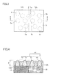
- Fig. 2 is a sectional view taken along line II-II of Fig. 3 .
- Fig. 3 is a plan view of region R shown in Fig. 2 , viewed from above the drawing sheet (the direction of arrow X).
- a plurality of n contact regions 5a are arranged in a mottled manner on main face 14A, of source region 14.
- a plurality of p contact regions 5b are arranged in a mottled manner on main face 18A of p region 18.
- N + source region 14 forms contact with p region 18 at a border 2.
- First region 5 may have, at border 2, a first pn contact region 5c in contact with both n + source region 14 and p + region 18.
- contact electrode 16 may include a third region 6 containing TiC.
- P contact region 5b, n contact region 5a, first pn contact region 5c and third region 6 have substantially a circle shape, for example, in plan view.
- first region 5 may be larger than the height of second region 3.
- the top of second region 3 is arranged to protrude from the first region.
- Second region 3 is formed to surround first region 5 in plan view.
- the height of the plurality of first regions 5 may differ from each other.
- the height of one first region 5 may be larger than the height of second region 3, and the height of another first region 5 may be smaller than the height of the second region.
- a plurality of p contact regions 5b may include a p contact region 5b higher than second region 3, and a p contact region 5b lower than second region 3.
- a plurality of n contact regions 5a may include an n contact region 5a higher than second region 3, and an n contact region 5a lower than second region 3.
- Second region 3 is formed to surround first region 5 in plan view.
- the left side corresponds to the side of protection electrode 19 (in other words, the side of surface 16A of contact electrode 16), whereas the right side corresponds to the side of silicon carbide substrate 10 (in other words, the side of back face 16B of the contact electrode).
- the concentration of atoms constituting contact electrode 16 by Auger electron spectroscopy, for example, there are more Al (aluminium) and O (oxygen) than Si (silicon) and C (carbon) at the side of surface 16A of contact electrode 16.
- Si silicon
- C carbon
- contact electrode 16 there is a region S where the number of C (carbon) atoms is larger than the number of Si (silicon) atoms.
- Contact electrode 16 having region S where the number of C (carbon) atoms is larger than the number of Si (silicon) atoms exhibits a lower contact resistance than contact electrode 16 absent of region S where the number of C (carbon) atoms is larger than the number of Si (silicon) atoms.
- the ratio of two arbitrary number of atoms from x, y and z is greater than or equal to 1/3 and less than or equal to 3.
- the number of atoms with a higher count divided by the number of atoms with a lower count is less than or equal to 3
- the number of atoms with a lower count divided by the number of atoms with a higher count is greater than or equal to 1/3.
- the number of Ti atoms is greater than or equal to 1/3 times and less than or equal to 3 times the number of Si atoms
- the number of Si atoms is greater than or equal to 1/3 times and less than or equal to 3 times the number of Al atoms
- the number of Al atoms is greater than or equal to 1/3 times and less than or equal to 3 times the number of Ti atoms.
- MOSFET 1 Under the state where a voltage less than or equal to a threshold value is applied to gate electrode 17, i.e. in an OFF state, reverse bias is established between p body 13 located immediately beneath gate oxide film 15 and n - SiC layer 12, leading to a non-conductive state.
- a voltage less than or equal to a threshold value is applied to gate electrode 17
- n - SiC layer 12 When positive voltage is applied to gate electrode 17, an inversion layer is formed at a channel region 13A that is a region of p body 13 in the neighborhood of gate oxide film 15 forming contact therewith.
- n + source region 14 and n - SiC layer 12 are electrically connected, whereby current flows between source electrode 22 and drain electrode 20.
- MOSFET I as a silicon carbide semiconductor device according to the first embodiment
- a silicon carbide substrate 10 is prepared by a substrate preparation step S10 ( Fig. 6 ).
- n - SiC layer 12 is formed on one main face 11A of n + SiC substrate 11.
- Epitaxial-growth can be implemented by employing a mixture gas of SiH 4 (silane) and C 3 H 8 (propane) as the raw material gas.
- N nitrogen
- n type impurities there can be formed an n - SiC layer 12 including n type impurities at a concentration lower than that of the n type impurities present in n' SiC substrate 11.
- an oxide film such as of SiO 2 is formed by CVD (Chemical Vapor Deposition), for example.
- CVD Chemical Vapor Deposition
- exposure and development are carried out to form a resist film having an opening at a region corresponding to the desired shape of p body 13.
- the oxide film is partially removed by RIE (Reactive Ion Etching), for example, to form a mask layer consisting of an oxide film having an opening pattern on n - SiC layer 12.
- RIE Reactive Ion Etching
- a mask layer having an opening at a region corresponding to the desired shape of n + source region 14 is formed.
- n type impurities such as P (phosphorus) are introduced by ion implantation to n - SiC layer 12 to form n + source region 14.
- a mask layer having an opening at a region corresponding to the desired shape of p + region 18 is formed.
- p type impurities such as Al or B are introduced by ion implantation into n - SiC layer 12 to form p + region 18.
- n - SiC layer 12 subjected to ion implantation is heated to approximately 1700°C in an atmosphere of Ar (argon) for example, and maintained for approximately 30 minutes.
- Ar argon
- gate oxide film 15 is formed by a gate insulation film formation step S20 ( Fig. 6 ).
- an n + substrate 11 formed with n - SiC layer 12 subjected to the foregoing step to include a desired ion implantation region is thermally oxidized.
- Thermal oxidation can be implemented by, for example, heating in an oxygen atmosphere at approximately 1300°C, maintained for approximately 40 minutes.
- a thermal oxidation film 15A (having a thickness of approximately 50 nm, for example) made of silicon dioxide (SiO 2 ) is formed on second main face 12B.
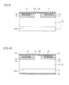
- a resist on thermal oxidation film 15A Following application of a resist on thermal oxidation film 15A, exposure and development are carried out to form a resist film having an opening corresponding to a region where contact electrode 16 (refer to Fig. 1 ) is to be formed. Then, using the resist film as a mask, the thermal oxidation film is removed partially by RIE, for example. Thus, gate oxide film 15 partially covering second main face 12B is formed.
- a contact electrode formation step S30 ( Fig. 6 ) is carried out.
- a metal layer 54 having a Ti portion, an Al portion, and a Si portion sequentially stacked on silicon carbide substrate 10 is formed on n + source region 14 and p + region 18.
- the thickness of the Ti portion, Al portion, and Si portion is, for example, 250 ⁇ , 200 ⁇ and 300 ⁇ , respectively.
- the thickness of metal layer 54 is preferably less than or equal to 1 ⁇ m, more preferably less than or equal to 500 nm, and further preferably less than or equal to 100 nm.
- a thinner metal layer 54 facilitates alloying.
- metal layer 54 is formed by sputtering or vapor deposition.
- metal layer 54 may have the Ti portion, Al portion, and Si portion take a juxtaposed structure aligned in a direction parallel to second main face 12B of silicon carbide substrate 10, or a structure aligned in a grid. Moreover, metal layer 54 may be a composite film having the Ti portion, Al portion, and Si portion mixed.
- the resist film is removed to eliminate (lift off) metal layer 54 on the resist film, leaving the region of metal layer 54 in contact with n + source region 14 and p + region 18.
- Metal layer 54 is alloyed by heating to form contact electrode 16 in ohmic contact with silicon carbide substrate 10. Specifically, in an inert gas atmosphere such as Ar, metal layer 54 and silicon carbide substrate 10 are heated to a temperature greater than or equal to 950°C and less than or equal to 1200°C, for example to 1000°C, and maintained for a period greater than or equal to 30 seconds and less than or equal to 300 seconds, for example. Accordingly, the Ti and Si contained in metal layer 54 are aggregated in the shape of an island to form first region 5 containing TiSi. In addition, Al spreads so as to surround the first layer, forming second region 3 containing Al.
- an inert gas atmosphere such as Ar
- contact electrode 16 is obtained, having first region 5 containing TiSi and second region 3 containing Al formed in a mottled manner.
- the annealing time is preferably lengthened.
- metal layer 54 and silicon carbide substrate 10 are heated at a temperature greater than or equal to 950°C and less than or equal to 1200°C, for example at 1000°C, and maintained for a period greater than or equal to 120 seconds and less than or equal to 150 seconds, for example.
- drain electrode 20 is formed at a face opposite to second main face 12B of silicon carbide substrate 10.
- Ni is sputtered on to form a Ni layer at the opposite side face.
- the Ni layer is annealed to form drain electrode 20.
- Metal layer 54 set forth above may be employed instead of this Ni layer.
- a gate electrode formation step S50 ( Fig. 6 ) is carried out to form a gate electrode 17.
- gate electrode 17 that is a conductor such as of polysilicon, Al, or the like is formed to extend from above one n + source region 14 to above the other n + source region 14, and in contact with gate oxide film 15.
- the polysilicon may include P (phosphorus) at a high concentration exceeding 1 ⁇ 10 20 cm -3
- protection electrode 19 is formed. By vapor deposition, for example, protection electrode 19 that is a conductor of Al is formed on surface 16A of contact electrode 16. Thus, source electrode 22 is completed.
- passivation film 21 is formed.
- passivation film 21 such as of SiO 2 , for example, is formed to pass over gate electrode 17, extending from above one protection electrode 19 to above the other protection electrode 19.
- Passivation film 21 can be formed by CVD, for example. Accordingly, MOSFET 1 is completed.
- the description is based on, but not limited to a planar type MOSFET as an example of a silicon carbide semiconductor device of the present invention.
- the silicon carbide semiconductor device may be a trench type MOSFET, an IGBT (Insulated Gate Bipolar Transistor), or the like.
- n contact region 5a containing TiSi is brought into contact with n + source region 14, whereas second region 3 containing Al is brought into contact with p + region 18. Accordingly, ohmic contact is allowed between n contact region 5a containing TiSi and n + source region 14 as well as between second region 3 containing Al and p + region 18. As a result, ohmic contact can be realized for both n + source region 14 and p + region 18.
- contact electrode 16 includes a region where the number of carbon atoms is larger than the number of silicon atoms. Accordingly, a low contact resistance can be realized as compared to a contact electrode 16 absent of a region where the number of carbon atoms is larger than the number of silicon atoms.
- second region 3 is formed to cover p contact region 5b and n contact region 5a. Therefore, the area of second region 3 facing protection electrode 19 becomes larger, allowing the adherence with protection electrode 19 to be improved.
- MOSFET 1 of the present embodiment when the number of Ti atoms is x, the number of Al atoms is y, and the number of Si atoms is z in contact electrode 16, the ratio of two arbitrary number of atoms from x, y and z is greater than or equal to 1/3 and less than or equal to 3. Accordingly, favorable ohmic contact can be realized for both an n type region and a p type region.
- the width W of each of p contact region 5b and n contact region 5a in a direction parallel to second main face 12B of silicon carbide substrate 10 is less than or equal to 500 nm. Accordingly, favorable ohmic contact can be realized for both n source region 14 and p + region 18.
- contact electrode 16 further includes third region 6 containing TiC. Therefore, favorable ohmic contact can be realized for both n + source region 14 and p + region 18.
- MOSFET silicon carbide semiconductor device
- 3 second region 5 first region, 5a n contact region; 5b p contact region; 6 third region; 10 silicon carbide substrate; 11 n + substrate; 12 n - SiC layer; 12B second main face; 13 p body; 13A channel region; 14 n + source region; 15 gate oxide film (insulation film); 15A thermal oxidation film; 16 contact electrode; 17 gate electrode; 18 p + region; 19 protection electrode; 20 drain electrode; 21 passivation film; 22 source electrode; 54 metal layer.
Abstract
Description
- The present invention relates to a silicon carbide semiconductor device, more particularly, a silicon carbide semiconductor device having a contact electrode in contact with a silicon carbide substrate.
- In recent years, silicon carbide substrates are now being used for manufacturing semiconductor devices. Silicon carbide has a bandgap larger than that of silicon. Therefore, a semiconductor device employing a silicon carbide substrate advantageously has a high breakdown voltage, low ON resistance, and less property deterioration in a high temperature environment.
- As a method of forming an ohmic electrode for silicon carbide, metal material including Ni or Al is vapor-deposited on an impurity region doped at high concentration. Then, the metal material is subjected to rapid thermal treatment at the temperature of approximately 1000°C to form a reaction layer. Thus, ohmic contact is established between the reaction layer and silicon carbide (refer to Non-Patent Document 1).
- [Non-Patent Document 1] Hiroyuki Matsunami et al. "Semiconductor SiC Technology and Application (Second Version)", Nikkan Kogyo Shimbunsha, September 30, 2011, pp. 298-309
- Although Ni allows ohmic contact with an n type impurity region formed at a silicon carbide substrate, Ni exhibits high contact resistance to a p type impurity region formed at the silicon carbide substrate. In contrast, Al allows ohmic contact with a p type impurity region formed at a silicon carbide substrate while exhibiting high contact resistance with an n type impurity region formed at the silicon carbide substrate. It was therefore extremely difficult to realize ohmic contact for both a p type impurity region and an n type impurity region formed at a silicon carbide substrate.
- An object of the present invention is to provide a silicon carbide semiconductor device having an electrode capable of ohmic contact with both a p type impurity region and an n type impurity region formed at a silicon carbide substrate.
- A silicon carbide semiconductor device according to the present invention includes a silicon carbide substrate, and a contact electrode. The silicon carbide substrate includes an n type region and a p type region in contact with the n type region. The contact electrode forms contact with the silicon carbide substrate. The contact electrode includes a first region containing TiSi, and a second region containing Al. The first region includes an n contact region in contact with the n type region, and a p contact region in contact with the p type region. The second region is formed in contact with the p type region and the n type region, and to surround the p contact region and the n contact region.
- As used herein, TiSi refers to a compound having Ti-Si bonding, and includes those with a Ti and Si composition ratio besides 1:1.
- According to the silicon carbide semiconductor device of the present invention, ohmic contact is allowed at a first region containing TiSi and an n type region, and at a second region containing Al and a p type region. As a result, ohmic contact can be established for both an n type region and a p type region.
- Preferably in the foregoing silicon carbide semiconductor device, the contact electrode includes a region where the number of carbon atoms is larger than the number of silicon atoms.
- Accordingly, low contact resistance can be realized, as compared to a contact electrode not including a region where the number of carbon atoms is larger than the number of silicon atoms.
- Preferably in the foregoing silicon carbide semiconductor device, the second region is formed to cover the p contact region and the n contact region. Accordingly, the area of the second region facing a protection electrode is increased, allowing the adherence with the protection electrode to be improved.
- Preferably in the foregoing silicon carbide semiconductor device, when the number of Ti atoms is x, the number of Al atoms is y, and the number of Si atoms is z in the contact electrode, the ratio of two arbitrary number of atoms from x, y and z is greater than or equal to 1/3 and less than or equal to 3. Accordingly, favorable ohmic contact can be realized for both an n type region and p type region.
- Preferably in the foregoing silicon carbide semiconductor device, the width of each of the p contact region and the n contact region in a direction parallel to the main face of the silicon carbide substrate is less than or equal to 500 nm. Accordingly, favorable ohmic contact can be realized for both an n type region and p type region.
- Preferably in the foregoing silicon carbide semiconductor device, the contact electrode further includes a third region containing TiC. As used herein, TiC refers to a compound having Ti-C bonding, and includes those with a Ti and C composition ratio besides 1:1. Accordingly, favorable ohmic contact with both an n type region and p type region can be realized.
- As apparent from the foregoing, a silicon carbide semiconductor device having an electrode capable of ohmic contact with both a p type impurity region and an n type impurity region formed at a silicon carbide substrate can be provided by the present invention.
-
-
Fig. 1 is a sectional view schematically representing a configuration of a silicon carbide semiconductor device according to an embodiment of the present invention. -
Fig. 2 is an enlarged sectional view of a region R ofFig. 1 . -
Fig. 3 is an enlarged plan view of a region R ofFig. 1 . -
Fig. 4 is an enlarged sectional view of a region R ofFig. 1 . -
Fig. 5 is an enlarged sectional view of a region R ofFig. 1 . -
Fig. 6 is a flowchart schematically representing a method for manufacturing a silicon carbide semiconductor device according to an embodiment of the present invention. -
Fig. 7 is a sectional view schematically representing a first step in a method for manufacturing a silicon carbide semiconductor device according to an embodiment of the present invention. -
Fig. 8 is a sectional view schematically representing a second step in a method for manufacturing a silicon carbide semiconductor device according to an embodiment of the present invention. -
Fig. 9 is a sectional view schematically representing a third step in a method for manufacturing a silicon carbide semiconductor device according to an embodiment of the present invention. -
Fig. 10 is a sectional view schematically representing a fourth step in a method for manufacturing a silicon carbide semiconductor device according to an embodiment of the present invention. -
Fig. 11 is a sectional view schematically representing a fifth step in a method for manufacturing a silicon carbide semiconductor device according to an embodiment of the present invention. -
Fig. 12 is a diagram representing the atom concentration in a contact electrode of a silicon carbide semiconductor device according to an embodiment of the present invention. - Embodiments of the present invention will be described hereinafter with reference to the drawings. In the drawings, the same or corresponding elements have the same reference characters allotted, and description thereof will not be repeated.
- First, a configuration of an MOSFET 1 (Metal Oxide Semiconductor Field Effect Transistor) as a silicon carbide semiconductor device according to an embodiment of the present invention will be described.
- Referring to
Fig. 1 ,MOSFET 1 includes asilicon carbide substrate 10.Silicon carbide substrate 10 includes an n+ substrate 11, an n- SiC layer 12,a p body 13, an n+ source region 14, and a p+ region 18. - N+ substrate 11 is a substrate of n conductivity type, formed of silicon carbide (SiC). N+ substrate 11 includes n type impurities of high concentration (impurities of n conductivity type), for example N (nitrogen).
- N- SiC layer 12 is a semiconductor layer of n conductivity type, formed of SiC. N- SiC layer 12 is formed on one
main face 11A of n+ substrate 11 to a thickness of approximately 10 µm, for example. The n type impurities in n- SiC layer 12 are N (nitrogen), for example, and present at a concentration lower than that of the n type impurities in n+ substrate 11, for example, present at the concentration of 5×1015 cm-3. - A pair of
p bodies 13 has p type conductivity. Each ofp bodies 13 constituting a pair is formed separated from the other so as to include a secondmain face 12B (substrate face) that is the main face at a side opposite to a firstmain face 12A that is the main face at the side of n+ substrate 11 in n- SiC layer 12. The p type impurities inp body 13 are Al (aluminium), B (boron), or the like. The p type impurities are present at a concentration lower than that of n type impurities included in n+ substrate 11, for example, present at the concentration of 1×1017 cm-3. - N+ source region 14 is an n type region having n type conductivity. N+ source region 14 is formed in each of
p bodies 13 constituting a pair so as to include a secondmain face 12B and surroundp body 13. N+ source region 14 includes n type impurities, for example P (phosphorus), at a concentration higher than that of the n type impurities in n- SiC layer 12, for example, at the concentration of 1×1020 cm-3 - P+ region 18 is a p type region having p type conductivity. P+ region 18 is formed to include, when viewed from n+ source region 14 formed in one of
p bodies 13 constituting a pair, secondmain face 12B, at the side opposite to n+ source region 14 formed in theother p body 13. P+ region 18 includes p type impurities, for example Al, B or the like, at a concentration higher than that of the p type impurities included inp body 13, for example at the concentration of 1 ×1020 cm-3. -
MOSFET 1 includes a gate oxide film 15 (insulation film) as a gate insulation film, agate electrode 17, a pair of contact electrodes 16 (source contact electrode), aprotection electrode 19, adrain electrode 20 and apassivation film 21. -
Gate oxide film 15 is formed in contact with and on secondmain face 12B of n- SiC layer 12 so as to extend from the top surface of one n+ source region 14 to the top surface of the other n+ source region 14.Gate oxide film 15 preferably includes at least any of a silicon oxide film and silicon nitride film, and is formed of silicon dioxide (SiO2), for example. -
Gate electrode 17 is arranged in contact withgate oxide film 15, so as to extend on and from one n+ source region 14 to the other n+ source region 14.Gate electrode 17 is formed of a conductor such as of polysilicon, Al, or the like. -
Contact electrode 16 is arranged to extend from above each of n+ source regions 14 constituting a pair as far as above p+ region 18 in the direction away fromgate oxide film 15, and is in contact with secondmain face 12B. Details of the configuration ofcontact electrode 16 will be described afterwards. -
Protection electrode 19 is formed in contact withcontact electrode 16, and made of a conductor such as of Al.Protection electrode 19 is electrically connected with n+ source region 14 viacontact electrode 16.Protection electrode 19 andcontact electrode 16 constitute asource electrode 22. -
Drain electrode 20 is formed in contact with the othermain face 11B that is the main face at the side opposite to onemain face 11A that is the main face at the side where n- SiC layer 12 is formed at n+ substrate 11.Drain electrode 20 may have a structure similar to that ofcontact electrode 16 set forth above, for example, or may be formed of another material allowing ohmic contact with n+ substrate 11, such as Ni (nickel). Accordingly,drain electrode 20 is electrically connected with n+ substrate 11. -
Passivation film 21 is formed to pass overgate electrode 17, extending from above oneprotection electrode 19 to above theother protection electrode 19.Passivation film 21 is formed of SiO2, for example, and functions to electrically insulateprotection electrode 19 andgate electrode 17 from outside, and to protectMOSFET 1. - The configuration of a region R of
MOSFET 1 inFig. 1 will be described in detail with reference toFigs. 2-5 . - Referring to
Fig. 2 , region R includes n+ source region 14,p region 18, andcontact electrode 16. P+ region 18 forms contact with n+ source region 14.Contact electrode 16 includes afirst region 5 containing TiSi, and asecond region 3 containing Al.First region 5 includes ann contact region 5a in contact with n+ source region 14 atmain face 14A, anda p contact region 5b in contact with p+ region 18 atmain face 18A.Second region 3 is formed to contact n+ source region 14 and p+ region 18, and to surroundp contact region 5b andn contact region 5a. -
Second region 3 may include a compound having Al-O bonding. Further,contact electrode 16 may contain carbon.First region 5 andsecond region 3 may also contain carbon. - As shown in
Fig. 2 ,second region 3 may be formed to have a thickness greater than the thickness offirst region 5, and to coverfirst region 5.P contact region 5b is arranged as an island onmain face 18A of p+ region 18, for example.N contact region 5a is arranged as an island onmain face 14A of n+ source region 14, for example. The width W of each ofp contact region 5b andn contact region 5a (specifically, the width ofp contact region 5b andn contact region 5a in the direction parallel to secondmain face 12B ofsilicon carbide substrate 10. Preferably, width W is greater than or equal to 10 nm and less than or equal to 100 nm, more preferably greater than or equal to 30 nm and less than or equal to 60 nm. The widths of n+ source region 14 and p+ region 18 are approximately 3.2 µm and approximately 1.8 µm, respectively. The thickness T ofcontact electrode 16 is, for example, approximately 100 nm.Fig. 2 is a sectional view taken along line II-II ofFig. 3 . -
Fig. 3 is a plan view of region R shown inFig. 2 , viewed from above the drawing sheet (the direction of arrow X). As shown inFig. 3 , a plurality ofn contact regions 5a are arranged in a mottled manner onmain face 14A, ofsource region 14. Further, a plurality ofp contact regions 5b are arranged in a mottled manner onmain face 18A ofp region 18. N+ source region 14 forms contact withp region 18 at aborder 2.First region 5 may have, atborder 2, a firstpn contact region 5c in contact with both n+ source region 14 and p+ region 18. Further,contact electrode 16 may include athird region 6 containing TiC.P contact region 5b,n contact region 5a, firstpn contact region 5c andthird region 6 have substantially a circle shape, for example, in plan view. - Referring to
Fig. 4 , the height offirst region 5 may be larger than the height ofsecond region 3. In this case, the top ofsecond region 3 is arranged to protrude from the first region.Second region 3 is formed to surroundfirst region 5 in plan view. - Referring to
Fig. 5 , the height of the plurality offirst regions 5 may differ from each other. Among the plurality offirst regions 5, the height of onefirst region 5 may be larger than the height ofsecond region 3, and the height of anotherfirst region 5 may be smaller than the height of the second region. Specifically, a plurality ofp contact regions 5b may includea p contact region 5b higher thansecond region 3, anda p contact region 5b lower thansecond region 3. Similarly, a plurality ofn contact regions 5a may include ann contact region 5a higher thansecond region 3, and ann contact region 5a lower thansecond region 3.Second region 3 is formed to surroundfirst region 5 in plan view. - Referring to
Fig. 12 , the distribution of atom concentration incontact electrode 16 will be described hereinafter. InFig. 12 , the left side corresponds to the side of protection electrode 19 (in other words, the side ofsurface 16A of contact electrode 16), whereas the right side corresponds to the side of silicon carbide substrate 10 (in other words, the side ofback face 16B of the contact electrode). Upon analyzing the concentration of atoms constitutingcontact electrode 16 by Auger electron spectroscopy, for example, there are more Al (aluminium) and O (oxygen) than Si (silicon) and C (carbon) at the side ofsurface 16A ofcontact electrode 16. However, at the side ofback face 16B ofcontact electrode 16, there are more Si and C than Al and O. - Preferably, at the side of
back face 16B ofcontact electrode 16, there is a region S where the number of C (carbon) atoms is larger than the number of Si (silicon) atoms.Contact electrode 16 having region S where the number of C (carbon) atoms is larger than the number of Si (silicon) atoms exhibits a lower contact resistance thancontact electrode 16 absent of region S where the number of C (carbon) atoms is larger than the number of Si (silicon) atoms. - Preferably, when the number of Ti (titanium) atoms is x, the number of Al (aluminium) atoms is y, and the number of Si (silicon) atoms is z, the ratio of two arbitrary number of atoms from x, y and z is greater than or equal to 1/3 and less than or equal to 3. In other words, the number of atoms with a higher count divided by the number of atoms with a lower count is less than or equal to 3, whereas the number of atoms with a lower count divided by the number of atoms with a higher count is greater than or equal to 1/3. For example, the number of Ti atoms is greater than or equal to 1/3 times and less than or equal to 3 times the number of Si atoms, the number of Si atoms is greater than or equal to 1/3 times and less than or equal to 3 times the number of Al atoms, and the number of Al atoms is greater than or equal to 1/3 times and less than or equal to 3 times the number of Ti atoms.
- The operation of
MOSFET 1 will be described hereinafter. Under the state where a voltage less than or equal to a threshold value is applied togate electrode 17, i.e. in an OFF state, reverse bias is established betweenp body 13 located immediately beneathgate oxide film 15 and n- SiC layer 12, leading to a non-conductive state. When positive voltage is applied togate electrode 17, an inversion layer is formed at achannel region 13A that is a region ofp body 13 in the neighborhood ofgate oxide film 15 forming contact therewith. As a result, n+ source region 14 and n- SiC layer 12 are electrically connected, whereby current flows betweensource electrode 22 anddrain electrode 20. - A method for manufacturing MOSFET I as a silicon carbide semiconductor device according to the first embodiment will be described hereinafter.
- Referring to
Figs. 7 and 8 , asilicon carbide substrate 10 is prepared by a substrate preparation step S10 (Fig. 6 ). - Specifically, by epitaxial-growth on n+ SiC substrate 11, n- SiC layer 12 is formed on one
main face 11A of n+ SiC substrate 11. Epitaxial-growth can be implemented by employing a mixture gas of SiH4 (silane) and C3H8 (propane) as the raw material gas. At this stage, N (nitrogen), for example, is introduced as the n type impurities. Accordingly, there can be formed an n- SiC layer 12 including n type impurities at a concentration lower than that of the n type impurities present in n'SiC substrate 11. - Then, on second
main face 12B, an oxide film such as of SiO2 is formed by CVD (Chemical Vapor Deposition), for example. Following application of a resist on the oxide film, exposure and development are carried out to form a resist film having an opening at a region corresponding to the desired shape ofp body 13. Using the resist film as a mask, the oxide film is partially removed by RIE (Reactive Ion Etching), for example, to form a mask layer consisting of an oxide film having an opening pattern on n- SiC layer 12. Then, upon removing the resist film, p type impurities such as Al are ion-implanted into n- SiC layer 12 using the mask layer as a mask to formp body 13 at n- SiC layer 12. - Then, upon removing the aforementioned oxide film used as a mask, a mask layer having an opening at a region corresponding to the desired shape of n+ source region 14 is formed. Using this mask layer as a mask, n type impurities such as P (phosphorus) are introduced by ion implantation to n- SiC layer 12 to form n+ source region 14. Then, a mask layer having an opening at a region corresponding to the desired shape of p+ region 18 is formed. Using this as a mask, p type impurities such as Al or B are introduced by ion implantation into n- SiC layer 12 to form p+ region 18.
- Then, a heat treatment to render active the impurities introduced by ion implantation is carried out. Specifically, n- SiC layer 12 subjected to ion implantation is heated to approximately 1700°C in an atmosphere of Ar (argon) for example, and maintained for approximately 30 minutes. Thus,
silicon carbide substrate 10 having secondmain face 12B (Fig. 8 ) is prepared. - Referring to
Fig. 9 , gate oxide film 15 (insulation film) is formed by a gate insulation film formation step S20 (Fig. 6 ). Specifically, an n+ substrate 11 formed with n- SiC layer 12 subjected to the foregoing step to include a desired ion implantation region is thermally oxidized. Thermal oxidation can be implemented by, for example, heating in an oxygen atmosphere at approximately 1300°C, maintained for approximately 40 minutes. Accordingly, athermal oxidation film 15A (having a thickness of approximately 50 nm, for example) made of silicon dioxide (SiO2) is formed on secondmain face 12B. - Following application of a resist on
thermal oxidation film 15A, exposure and development are carried out to form a resist film having an opening corresponding to a region where contact electrode 16 (refer toFig. 1 ) is to be formed. Then, using the resist film as a mask, the thermal oxidation film is removed partially by RIE, for example. Thus,gate oxide film 15 partially covering secondmain face 12B is formed. - Referring to
Fig. 10 , a contact electrode formation step S30 (Fig. 6 ) is carried out. - Specifically, a
metal layer 54 having a Ti portion, an Al portion, and a Si portion sequentially stacked onsilicon carbide substrate 10 is formed on n+ source region 14 and p+ region 18. The thickness of the Ti portion, Al portion, and Si portion is, for example, 250Å, 200Å and 300Å, respectively. The thickness ofmetal layer 54 is preferably less than or equal to 1 µm, more preferably less than or equal to 500 nm, and further preferably less than or equal to 100 nm. Athinner metal layer 54 facilitates alloying. Preferably,metal layer 54 is formed by sputtering or vapor deposition. - Further,
metal layer 54 may have the Ti portion, Al portion, and Si portion take a juxtaposed structure aligned in a direction parallel to secondmain face 12B ofsilicon carbide substrate 10, or a structure aligned in a grid. Moreover,metal layer 54 may be a composite film having the Ti portion, Al portion, and Si portion mixed. - Then, the resist film is removed to eliminate (lift off)
metal layer 54 on the resist film, leaving the region ofmetal layer 54 in contact with n+ source region 14 and p+ region 18. - Referring to
Fig. 11 following formation ofmetal layer 54, an annealing step is carried out.Metal layer 54 is alloyed by heating to formcontact electrode 16 in ohmic contact withsilicon carbide substrate 10. Specifically, in an inert gas atmosphere such as Ar,metal layer 54 andsilicon carbide substrate 10 are heated to a temperature greater than or equal to 950°C and less than or equal to 1200°C, for example to 1000°C, and maintained for a period greater than or equal to 30 seconds and less than or equal to 300 seconds, for example. Accordingly, the Ti and Si contained inmetal layer 54 are aggregated in the shape of an island to formfirst region 5 containing TiSi. In addition, Al spreads so as to surround the first layer, formingsecond region 3 containing Al. Thus,contact electrode 16 is obtained, havingfirst region 5 containing TiSi andsecond region 3 containing Al formed in a mottled manner. In order to form acontact electrode 16 having such a configuration, the annealing time is preferably lengthened. For example,metal layer 54 andsilicon carbide substrate 10 are heated at a temperature greater than or equal to 950°C and less than or equal to 1200°C, for example at 1000°C, and maintained for a period greater than or equal to 120 seconds and less than or equal to 150 seconds, for example. - Then, by a drain electrode formation step S40 (
Fig. 6 ),drain electrode 20 is formed at a face opposite to secondmain face 12B ofsilicon carbide substrate 10. For example, Ni is sputtered on to form a Ni layer at the opposite side face. The Ni layer is annealed to formdrain electrode 20.Metal layer 54 set forth above may be employed instead of this Ni layer. - Referring to
Fig. 1 again, a gate electrode formation step S50 (Fig. 6 ) is carried out to form agate electrode 17. In this step,gate electrode 17 that is a conductor such as of polysilicon, Al, or the like is formed to extend from above one n+ source region 14 to above the other n+ source region 14, and in contact withgate oxide film 15. In the case where polysilicon is employed as the material of the gate electrode, the polysilicon may include P (phosphorus) at a high concentration exceeding 1×1020 cm-3 Next, at a protection electrode formation step S60 (Fig. 6 ),protection electrode 19 is formed. By vapor deposition, for example,protection electrode 19 that is a conductor of Al is formed onsurface 16A ofcontact electrode 16. Thus,source electrode 22 is completed. - At the next passivation film formation step S70 (
Fig. 6 ),passivation film 21 is formed. In this step,passivation film 21 such as of SiO2, for example, is formed to pass overgate electrode 17, extending from above oneprotection electrode 19 to above theother protection electrode 19.Passivation film 21 can be formed by CVD, for example. Accordingly,MOSFET 1 is completed. - A configuration in which the n type and p type in the foregoing embodiment are exchanged may be employed. Furthermore, the description is based on, but not limited to a planar type MOSFET as an example of a silicon carbide semiconductor device of the present invention. For example, the silicon carbide semiconductor device may be a trench type MOSFET, an IGBT (Insulated Gate Bipolar Transistor), or the like.
- The functional effect of the present embodiment will be described hereinafter.
- According to
MOSFET 1 of the present embodiment,n contact region 5a containing TiSi is brought into contact with n+ source region 14, whereassecond region 3 containing Al is brought into contact with p+ region 18. Accordingly, ohmic contact is allowed betweenn contact region 5a containing TiSi and n+ source region 14 as well as betweensecond region 3 containing Al and p+ region 18. As a result, ohmic contact can be realized for both n+ source region 14 and p+ region 18. - According to
MOSFET 1 of the present embodiment,contact electrode 16 includes a region where the number of carbon atoms is larger than the number of silicon atoms. Accordingly, a low contact resistance can be realized as compared to acontact electrode 16 absent of a region where the number of carbon atoms is larger than the number of silicon atoms. - Furthermore, according to
MOSFET 1 of the present embodiment,second region 3 is formed to coverp contact region 5b andn contact region 5a. Therefore, the area ofsecond region 3 facingprotection electrode 19 becomes larger, allowing the adherence withprotection electrode 19 to be improved. - Further, according to
MOSFET 1 of the present embodiment, when the number of Ti atoms is x, the number of Al atoms is y, and the number of Si atoms is z incontact electrode 16, the ratio of two arbitrary number of atoms from x, y and z is greater than or equal to 1/3 and less than or equal to 3. Accordingly, favorable ohmic contact can be realized for both an n type region and a p type region. - Furthermore, according to
MOSFET 1 of the present embodiment, the width W of each ofp contact region 5b andn contact region 5a in a direction parallel to secondmain face 12B ofsilicon carbide substrate 10 is less than or equal to 500 nm. Accordingly, favorable ohmic contact can be realized for bothn source region 14 and p+ region 18. - Moreover, according to
MOSFET 1 of the present embodiment,contact electrode 16 further includesthird region 6 containing TiC. Therefore, favorable ohmic contact can be realized for both n+ source region 14 and p+ region 18. - It should be understood that the embodiments disclosed herein are illustrative and nonrestrictive in every respect. The scope of the present invention is defined by the terms of the claims, rather than the description set forth above, and is intended to include any modification within the scope and meaning equivalent to the terms of the claims.
- 1 MOSFET (silicon carbide semiconductor device); 3 second region; 5 first region, 5a n contact region; 5b p contact region; 6 third region; 10 silicon carbide substrate; 11 n+ substrate; 12 n- SiC layer; 12B second main face; 13 p body; 13A channel region; 14 n+ source region; 15 gate oxide film (insulation film); 15A thermal oxidation film; 16 contact electrode; 17 gate electrode; 18 p+ region; 19 protection electrode; 20 drain electrode; 21 passivation film; 22 source electrode; 54 metal layer.
Claims (6)
- A silicon carbide semiconductor device comprising:a silicon carbide substrate including an n type region and a p type region in contact with said n type region, anda contact electrode in contact with said silicon carbide substrate,said contact electrode including a first region containing TiSi and a second region containing Al,said first region including an n contact region in contact with said n type region and a p contact region in contact with said p type region,said second region formed in contact with said p type region and said n type region, and surrounding said p contact region and said n contact region.
- The silicon carbide semiconductor device according to claim 1, wherein said contact electrode includes a region where the number of carbon atoms is larger than the number of silicon atoms.
- The silicon carbide semiconductor device according to claim 1 or 2,
wherein said second region is formed to cover said p contact region and said n contact region. - The silicon carbide semiconductor device according to any one of claims 1-3, wherein, when the number of Ti atoms is x, the number of Al atoms is y, and the number of Si atoms is z in said contact electrode, a ratio of two arbitrary number of atoms from x, y and z is greater than or equal to 1/3 and less than or equal to 3.
- The silicon carbide semiconductor device according to any one of claims 1-4, wherein a width of each of said p contact region and said n contact region in a direction parallel to a main face of said silicon carbide substrate is less than or equal to 500 nm.
- The silicon carbide semiconductor device according to any one of claims 1-5, wherein said contact electrode further includes a third region containing TiC.
Applications Claiming Priority (2)
| Application Number | Priority Date | Filing Date | Title |
|---|---|---|---|
| JP2012139386A JP2014003253A (en) | 2012-06-21 | 2012-06-21 | Silicon carbide semiconductor device |
| PCT/JP2013/062210 WO2013190907A1 (en) | 2012-06-21 | 2013-04-25 | Silicon carbide semiconductor device |
Publications (2)
| Publication Number | Publication Date |
|---|---|
| EP2866263A1 true EP2866263A1 (en) | 2015-04-29 |
| EP2866263A4 EP2866263A4 (en) | 2016-02-10 |
Family
ID=49768514
Family Applications (1)
| Application Number | Title | Priority Date | Filing Date |
|---|---|---|---|
| EP13807640.1A Withdrawn EP2866263A4 (en) | 2012-06-21 | 2013-04-25 | Silicon carbide semiconductor device |
Country Status (5)
| Country | Link |
|---|---|
| US (1) | US8729567B2 (en) |
| EP (1) | EP2866263A4 (en) |
| JP (1) | JP2014003253A (en) |
| CN (1) | CN104285299A (en) |
| WO (1) | WO2013190907A1 (en) |
Families Citing this family (3)
| Publication number | Priority date | Publication date | Assignee | Title |
|---|---|---|---|---|
| JP2014003253A (en) * | 2012-06-21 | 2014-01-09 | Sumitomo Electric Ind Ltd | Silicon carbide semiconductor device |
| JP6922202B2 (en) | 2016-12-07 | 2021-08-18 | 富士電機株式会社 | Semiconductor devices and methods for manufacturing semiconductor devices |
| DE102016125030A1 (en) * | 2016-12-20 | 2018-06-21 | Infineon Technologies Ag | Forming a metal contact layer on silicon carbide and semiconductor device having a metal contact structure |
Family Cites Families (11)
| Publication number | Priority date | Publication date | Assignee | Title |
|---|---|---|---|---|
| JP3759145B2 (en) * | 2003-03-18 | 2006-03-22 | 松下電器産業株式会社 | Silicon carbide semiconductor device and manufacturing method thereof |
| US7217954B2 (en) | 2003-03-18 | 2007-05-15 | Matsushita Electric Industrial Co., Ltd. | Silicon carbide semiconductor device and method for fabricating the same |
| JP2006332199A (en) * | 2005-05-24 | 2006-12-07 | Shindengen Electric Mfg Co Ltd | SiC SEMICONDUCTOR DEVICE |
| WO2008018342A1 (en) * | 2006-08-09 | 2008-02-14 | National Institute Of Advanced Industrial Science And Technology | Silicon carbide semiconductor device and method for fabricating the same |
| JP4960125B2 (en) | 2007-03-22 | 2012-06-27 | 株式会社東芝 | Semiconductor device and manufacturing method thereof |
| EP2280417B1 (en) * | 2008-04-15 | 2015-07-22 | Sumitomo Electric Industries, Ltd. | Semiconductor device and method for manufacturing the same |
| JP5668414B2 (en) * | 2010-11-01 | 2015-02-12 | 住友電気工業株式会社 | Manufacturing method of semiconductor device |
| JP2012253293A (en) * | 2011-06-07 | 2012-12-20 | Sumitomo Electric Ind Ltd | Semiconductor device |
| JP5728339B2 (en) * | 2011-09-08 | 2015-06-03 | 株式会社東芝 | Semiconductor device and manufacturing method of semiconductor device |
| JP5646527B2 (en) * | 2012-03-02 | 2014-12-24 | 株式会社東芝 | Semiconductor device and manufacturing method of semiconductor device |
| JP2014003253A (en) * | 2012-06-21 | 2014-01-09 | Sumitomo Electric Ind Ltd | Silicon carbide semiconductor device |
-
2012
- 2012-06-21 JP JP2012139386A patent/JP2014003253A/en not_active Withdrawn
-
2013
- 2013-04-25 WO PCT/JP2013/062210 patent/WO2013190907A1/en active Application Filing
- 2013-04-25 CN CN201380024867.4A patent/CN104285299A/en active Pending
- 2013-04-25 EP EP13807640.1A patent/EP2866263A4/en not_active Withdrawn
- 2013-05-16 US US13/895,910 patent/US8729567B2/en active Active
Also Published As
| Publication number | Publication date |
|---|---|
| WO2013190907A1 (en) | 2013-12-27 |
| US8729567B2 (en) | 2014-05-20 |
| CN104285299A (en) | 2015-01-14 |
| JP2014003253A (en) | 2014-01-09 |
| EP2866263A4 (en) | 2016-02-10 |
| US20130341647A1 (en) | 2013-12-26 |
Similar Documents
| Publication | Publication Date | Title |
|---|---|---|
| US9437682B2 (en) | Semiconductor device and semiconductor device manufacturing method | |
| KR101442886B1 (en) | Semiconductor device and method for manufacturing the same | |
| WO2010110246A1 (en) | Semiconductor device | |
| JP5391643B2 (en) | Silicon carbide semiconductor device and manufacturing method thereof | |
| US8643065B2 (en) | Semiconductor device and method for manufacturing the same | |
| WO2012165008A1 (en) | Silicon carbide semiconductor device and method for manufacturing same | |
| WO2011128994A1 (en) | Silicon carbide semiconductor device and method for manufacturing same | |
| US20150287817A1 (en) | Silicon carbide semiconductor device and method for manufacturing same | |
| EP2637213A1 (en) | Semiconductor device and manufacturing method therefor | |
| JP5834801B2 (en) | Semiconductor device manufacturing method and semiconductor device | |
| US8809945B2 (en) | Semiconductor device having angled trench walls | |
| JP5802492B2 (en) | Semiconductor device and manufacturing method thereof | |
| EP2866263A1 (en) | Silicon carbide semiconductor device | |
| US20160163817A1 (en) | Method for manufacturing silicon carbide semiconductor device | |
| US20160056040A1 (en) | Method for manufacturing silicon carbide semiconductor device | |
| US8748276B2 (en) | Method for manufacturing semiconductor device | |
| US8866156B2 (en) | Silicon carbide semiconductor device and method for manufacturing same | |
| US20160133707A1 (en) | Silicon carbide semiconductor device and method for manufacturing same | |
| WO2022270245A1 (en) | Silicon carbide semiconductor device | |
| JP2023104657A (en) | Silicon carbide semiconductor device | |
| JP2015115570A (en) | Silicon carbide semiconductor device and method of manufacturing the same | |
| JP2023023614A (en) | Silicon carbide semiconductor device | |
| JP2023057352A (en) | Silicon carbide semiconductor device and manufacturing method of silicon carbide semiconductor device | |
| JP5991629B2 (en) | Semiconductor device and manufacturing method of semiconductor device |
Legal Events
| Date | Code | Title | Description |
|---|---|---|---|
| PUAI | Public reference made under article 153(3) epc to a published international application that has entered the european phase |
Free format text: ORIGINAL CODE: 0009012 |
|
| 17P | Request for examination filed |
Effective date: 20141118 |
|
| AK | Designated contracting states |
Kind code of ref document: A1 Designated state(s): AL AT BE BG CH CY CZ DE DK EE ES FI FR GB GR HR HU IE IS IT LI LT LU LV MC MK MT NL NO PL PT RO RS SE SI SK SM TR |
|
| AX | Request for extension of the european patent |
Extension state: BA ME |
|
| DAX | Request for extension of the european patent (deleted) | ||
| RA4 | Supplementary search report drawn up and despatched (corrected) |
Effective date: 20160111 |
|
| RIC1 | Information provided on ipc code assigned before grant |
Ipc: H01L 29/78 20060101ALI20160104BHEP Ipc: H01L 21/336 20060101ALI20160104BHEP Ipc: H01L 29/41 20060101AFI20160104BHEP Ipc: H01L 29/417 20060101ALI20160104BHEP Ipc: H01L 29/12 20060101ALI20160104BHEP Ipc: H01L 21/28 20060101ALI20160104BHEP |
|
| STAA | Information on the status of an ep patent application or granted ep patent |
Free format text: STATUS: THE APPLICATION IS DEEMED TO BE WITHDRAWN |
|
| 18D | Application deemed to be withdrawn |
Effective date: 20160809 |