JP2014003253A - Silicon carbide semiconductor device - Google Patents
Silicon carbide semiconductor device Download PDFInfo
- Publication number
- JP2014003253A JP2014003253A JP2012139386A JP2012139386A JP2014003253A JP 2014003253 A JP2014003253 A JP 2014003253A JP 2012139386 A JP2012139386 A JP 2012139386A JP 2012139386 A JP2012139386 A JP 2012139386A JP 2014003253 A JP2014003253 A JP 2014003253A
- Authority
- JP
- Japan
- Prior art keywords
- region
- contact
- silicon carbide
- electrode
- type
- Prior art date
- Legal status (The legal status is an assumption and is not a legal conclusion. Google has not performed a legal analysis and makes no representation as to the accuracy of the status listed.)
- Withdrawn
Links
- 229910010271 silicon carbide Inorganic materials 0.000 title claims abstract description 96
- HBMJWWWQQXIZIP-UHFFFAOYSA-N silicon carbide Chemical compound [Si+]#[C-] HBMJWWWQQXIZIP-UHFFFAOYSA-N 0.000 title claims abstract description 77
- 239000004065 semiconductor Substances 0.000 title claims abstract description 38
- 239000000758 substrate Substances 0.000 claims abstract description 45
- 229910008484 TiSi Inorganic materials 0.000 claims abstract description 10
- 125000004429 atom Chemical group 0.000 claims description 27
- XUIMIQQOPSSXEZ-UHFFFAOYSA-N Silicon Chemical group [Si] XUIMIQQOPSSXEZ-UHFFFAOYSA-N 0.000 claims description 11
- 125000004432 carbon atom Chemical group C* 0.000 claims description 5
- 239000012535 impurity Substances 0.000 abstract description 30
- 229910052751 metal Inorganic materials 0.000 description 16
- 239000002184 metal Substances 0.000 description 16
- 230000001681 protective effect Effects 0.000 description 14
- 239000010936 titanium Substances 0.000 description 12
- 238000000034 method Methods 0.000 description 9
- PXHVJJICTQNCMI-UHFFFAOYSA-N nickel Substances [Ni] PXHVJJICTQNCMI-UHFFFAOYSA-N 0.000 description 9
- 238000004519 manufacturing process Methods 0.000 description 8
- 238000002161 passivation Methods 0.000 description 8
- IJGRMHOSHXDMSA-UHFFFAOYSA-N Atomic nitrogen Chemical compound N#N IJGRMHOSHXDMSA-UHFFFAOYSA-N 0.000 description 6
- OKTJSMMVPCPJKN-UHFFFAOYSA-N Carbon Chemical compound [C] OKTJSMMVPCPJKN-UHFFFAOYSA-N 0.000 description 6
- 229910052782 aluminium Inorganic materials 0.000 description 6
- 229910004298 SiO 2 Inorganic materials 0.000 description 5
- VYPSYNLAJGMNEJ-UHFFFAOYSA-N Silicium dioxide Chemical compound O=[Si]=O VYPSYNLAJGMNEJ-UHFFFAOYSA-N 0.000 description 5
- 229910052799 carbon Inorganic materials 0.000 description 5
- 229910052710 silicon Inorganic materials 0.000 description 5
- 230000015572 biosynthetic process Effects 0.000 description 4
- 239000004020 conductor Substances 0.000 description 4
- 238000005468 ion implantation Methods 0.000 description 4
- 229910021420 polycrystalline silicon Inorganic materials 0.000 description 4
- 229920005591 polysilicon Polymers 0.000 description 4
- OAICVXFJPJFONN-UHFFFAOYSA-N Phosphorus Chemical compound [P] OAICVXFJPJFONN-UHFFFAOYSA-N 0.000 description 3
- 238000000137 annealing Methods 0.000 description 3
- 229910052796 boron Inorganic materials 0.000 description 3
- 238000005229 chemical vapour deposition Methods 0.000 description 3
- 150000001875 compounds Chemical class 0.000 description 3
- 238000010438 heat treatment Methods 0.000 description 3
- 229910052757 nitrogen Inorganic materials 0.000 description 3
- 229910052760 oxygen Inorganic materials 0.000 description 3
- 229910052698 phosphorus Inorganic materials 0.000 description 3
- 239000011574 phosphorus Substances 0.000 description 3
- 238000001020 plasma etching Methods 0.000 description 3
- 229910052719 titanium Inorganic materials 0.000 description 3
- XKRFYHLGVUSROY-UHFFFAOYSA-N Argon Chemical compound [Ar] XKRFYHLGVUSROY-UHFFFAOYSA-N 0.000 description 2
- ATUOYWHBWRKTHZ-UHFFFAOYSA-N Propane Chemical compound CCC ATUOYWHBWRKTHZ-UHFFFAOYSA-N 0.000 description 2
- XAGFODPZIPBFFR-UHFFFAOYSA-N aluminium Chemical compound [Al] XAGFODPZIPBFFR-UHFFFAOYSA-N 0.000 description 2
- QVGXLLKOCUKJST-UHFFFAOYSA-N atomic oxygen Chemical compound [O] QVGXLLKOCUKJST-UHFFFAOYSA-N 0.000 description 2
- 238000006243 chemical reaction Methods 0.000 description 2
- 239000007789 gas Substances 0.000 description 2
- 239000000463 material Substances 0.000 description 2
- 239000007769 metal material Substances 0.000 description 2
- 229910052759 nickel Inorganic materials 0.000 description 2
- 239000001301 oxygen Substances 0.000 description 2
- 239000010703 silicon Substances 0.000 description 2
- 235000012239 silicon dioxide Nutrition 0.000 description 2
- 239000000377 silicon dioxide Substances 0.000 description 2
- 238000004544 sputter deposition Methods 0.000 description 2
- 238000007740 vapor deposition Methods 0.000 description 2
- 229910018516 Al—O Inorganic materials 0.000 description 1
- ZOXJGFHDIHLPTG-UHFFFAOYSA-N Boron Chemical compound [B] ZOXJGFHDIHLPTG-UHFFFAOYSA-N 0.000 description 1
- 229910052581 Si3N4 Inorganic materials 0.000 description 1
- BLRPTPMANUNPDV-UHFFFAOYSA-N Silane Chemical compound [SiH4] BLRPTPMANUNPDV-UHFFFAOYSA-N 0.000 description 1
- 229910004339 Ti-Si Inorganic materials 0.000 description 1
- RTAQQCXQSZGOHL-UHFFFAOYSA-N Titanium Chemical group [Ti] RTAQQCXQSZGOHL-UHFFFAOYSA-N 0.000 description 1
- 229910010978 Ti—Si Inorganic materials 0.000 description 1
- 230000003213 activating effect Effects 0.000 description 1
- 238000005275 alloying Methods 0.000 description 1
- AZDRQVAHHNSJOQ-UHFFFAOYSA-N alumane Chemical group [AlH3] AZDRQVAHHNSJOQ-UHFFFAOYSA-N 0.000 description 1
- 229910052786 argon Inorganic materials 0.000 description 1
- 230000015556 catabolic process Effects 0.000 description 1
- 230000006866 deterioration Effects 0.000 description 1
- 238000009826 distribution Methods 0.000 description 1
- 230000000694 effects Effects 0.000 description 1
- 238000005516 engineering process Methods 0.000 description 1
- 230000005669 field effect Effects 0.000 description 1
- 239000011261 inert gas Substances 0.000 description 1
- 229910044991 metal oxide Inorganic materials 0.000 description 1
- 150000004706 metal oxides Chemical class 0.000 description 1
- 238000002156 mixing Methods 0.000 description 1
- 238000012986 modification Methods 0.000 description 1
- 230000004048 modification Effects 0.000 description 1
- 230000003647 oxidation Effects 0.000 description 1
- 238000007254 oxidation reaction Methods 0.000 description 1
- 238000002360 preparation method Methods 0.000 description 1
- 239000001294 propane Substances 0.000 description 1
- 239000002994 raw material Substances 0.000 description 1
- 238000000682 scanning probe acoustic microscopy Methods 0.000 description 1
- 229910000077 silane Inorganic materials 0.000 description 1
- HQVNEWCFYHHQES-UHFFFAOYSA-N silicon nitride Chemical compound N12[Si]34N5[Si]62N3[Si]51N64 HQVNEWCFYHHQES-UHFFFAOYSA-N 0.000 description 1
- 229910052814 silicon oxide Inorganic materials 0.000 description 1
Images


Classifications
-
- H—ELECTRICITY
- H01—ELECTRIC ELEMENTS
- H01L—SEMICONDUCTOR DEVICES NOT COVERED BY CLASS H10
- H01L29/00—Semiconductor devices adapted for rectifying, amplifying, oscillating or switching, or capacitors or resistors with at least one potential-jump barrier or surface barrier, e.g. PN junction depletion layer or carrier concentration layer; Details of semiconductor bodies or of electrodes thereof ; Multistep manufacturing processes therefor
- H01L29/66—Types of semiconductor device ; Multistep manufacturing processes therefor
- H01L29/68—Types of semiconductor device ; Multistep manufacturing processes therefor controllable by only the electric current supplied, or only the electric potential applied, to an electrode which does not carry the current to be rectified, amplified or switched
- H01L29/76—Unipolar devices, e.g. field effect transistors
- H01L29/772—Field effect transistors
- H01L29/78—Field effect transistors with field effect produced by an insulated gate
- H01L29/7801—DMOS transistors, i.e. MISFETs with a channel accommodating body or base region adjoining a drain drift region
- H01L29/7802—Vertical DMOS transistors, i.e. VDMOS transistors
-
- H—ELECTRICITY
- H01—ELECTRIC ELEMENTS
- H01L—SEMICONDUCTOR DEVICES NOT COVERED BY CLASS H10
- H01L29/00—Semiconductor devices adapted for rectifying, amplifying, oscillating or switching, or capacitors or resistors with at least one potential-jump barrier or surface barrier, e.g. PN junction depletion layer or carrier concentration layer; Details of semiconductor bodies or of electrodes thereof ; Multistep manufacturing processes therefor
- H01L29/66—Types of semiconductor device ; Multistep manufacturing processes therefor
- H01L29/68—Types of semiconductor device ; Multistep manufacturing processes therefor controllable by only the electric current supplied, or only the electric potential applied, to an electrode which does not carry the current to be rectified, amplified or switched
- H01L29/76—Unipolar devices, e.g. field effect transistors
- H01L29/772—Field effect transistors
- H01L29/78—Field effect transistors with field effect produced by an insulated gate
-
- H—ELECTRICITY
- H01—ELECTRIC ELEMENTS
- H01L—SEMICONDUCTOR DEVICES NOT COVERED BY CLASS H10
- H01L21/00—Processes or apparatus adapted for the manufacture or treatment of semiconductor or solid state devices or of parts thereof
- H01L21/02—Manufacture or treatment of semiconductor devices or of parts thereof
- H01L21/04—Manufacture or treatment of semiconductor devices or of parts thereof the devices having at least one potential-jump barrier or surface barrier, e.g. PN junction, depletion layer or carrier concentration layer
- H01L21/0445—Manufacture or treatment of semiconductor devices or of parts thereof the devices having at least one potential-jump barrier or surface barrier, e.g. PN junction, depletion layer or carrier concentration layer the devices having semiconductor bodies comprising crystalline silicon carbide
- H01L21/048—Making electrodes
- H01L21/0485—Ohmic electrodes
-
- H—ELECTRICITY
- H01—ELECTRIC ELEMENTS
- H01L—SEMICONDUCTOR DEVICES NOT COVERED BY CLASS H10
- H01L21/00—Processes or apparatus adapted for the manufacture or treatment of semiconductor or solid state devices or of parts thereof
- H01L21/02—Manufacture or treatment of semiconductor devices or of parts thereof
- H01L21/04—Manufacture or treatment of semiconductor devices or of parts thereof the devices having at least one potential-jump barrier or surface barrier, e.g. PN junction, depletion layer or carrier concentration layer
- H01L21/18—Manufacture or treatment of semiconductor devices or of parts thereof the devices having at least one potential-jump barrier or surface barrier, e.g. PN junction, depletion layer or carrier concentration layer the devices having semiconductor bodies comprising elements of Group IV of the Periodic System or AIIIBV compounds with or without impurities, e.g. doping materials
- H01L21/28—Manufacture of electrodes on semiconductor bodies using processes or apparatus not provided for in groups H01L21/20 - H01L21/268
-
- H—ELECTRICITY
- H01—ELECTRIC ELEMENTS
- H01L—SEMICONDUCTOR DEVICES NOT COVERED BY CLASS H10
- H01L29/00—Semiconductor devices adapted for rectifying, amplifying, oscillating or switching, or capacitors or resistors with at least one potential-jump barrier or surface barrier, e.g. PN junction depletion layer or carrier concentration layer; Details of semiconductor bodies or of electrodes thereof ; Multistep manufacturing processes therefor
- H01L29/02—Semiconductor bodies ; Multistep manufacturing processes therefor
- H01L29/12—Semiconductor bodies ; Multistep manufacturing processes therefor characterised by the materials of which they are formed
- H01L29/16—Semiconductor bodies ; Multistep manufacturing processes therefor characterised by the materials of which they are formed including, apart from doping materials or other impurities, only elements of Group IV of the Periodic System
- H01L29/1608—Silicon carbide
-
- H—ELECTRICITY
- H01—ELECTRIC ELEMENTS
- H01L—SEMICONDUCTOR DEVICES NOT COVERED BY CLASS H10
- H01L29/00—Semiconductor devices adapted for rectifying, amplifying, oscillating or switching, or capacitors or resistors with at least one potential-jump barrier or surface barrier, e.g. PN junction depletion layer or carrier concentration layer; Details of semiconductor bodies or of electrodes thereof ; Multistep manufacturing processes therefor
- H01L29/40—Electrodes ; Multistep manufacturing processes therefor
- H01L29/41—Electrodes ; Multistep manufacturing processes therefor characterised by their shape, relative sizes or dispositions
- H01L29/417—Electrodes ; Multistep manufacturing processes therefor characterised by their shape, relative sizes or dispositions carrying the current to be rectified, amplified or switched
- H01L29/41725—Source or drain electrodes for field effect devices
-
- H—ELECTRICITY
- H01—ELECTRIC ELEMENTS
- H01L—SEMICONDUCTOR DEVICES NOT COVERED BY CLASS H10
- H01L29/00—Semiconductor devices adapted for rectifying, amplifying, oscillating or switching, or capacitors or resistors with at least one potential-jump barrier or surface barrier, e.g. PN junction depletion layer or carrier concentration layer; Details of semiconductor bodies or of electrodes thereof ; Multistep manufacturing processes therefor
- H01L29/40—Electrodes ; Multistep manufacturing processes therefor
- H01L29/43—Electrodes ; Multistep manufacturing processes therefor characterised by the materials of which they are formed
- H01L29/45—Ohmic electrodes
-
- H—ELECTRICITY
- H01—ELECTRIC ELEMENTS
- H01L—SEMICONDUCTOR DEVICES NOT COVERED BY CLASS H10
- H01L29/00—Semiconductor devices adapted for rectifying, amplifying, oscillating or switching, or capacitors or resistors with at least one potential-jump barrier or surface barrier, e.g. PN junction depletion layer or carrier concentration layer; Details of semiconductor bodies or of electrodes thereof ; Multistep manufacturing processes therefor
- H01L29/66—Types of semiconductor device ; Multistep manufacturing processes therefor
- H01L29/66007—Multistep manufacturing processes
- H01L29/66053—Multistep manufacturing processes of devices having a semiconductor body comprising crystalline silicon carbide
- H01L29/66068—Multistep manufacturing processes of devices having a semiconductor body comprising crystalline silicon carbide the devices being controllable only by the electric current supplied or the electric potential applied, to an electrode which does not carry the current to be rectified, amplified or switched, e.g. three-terminal devices
Abstract
Description
本発明は炭化珪素半導体装置に関し、より特定的には、炭化珪素基板と接するコンタクト電極を有する炭化珪素半導体装置に関する。 The present invention relates to a silicon carbide semiconductor device, and more particularly to a silicon carbide semiconductor device having a contact electrode in contact with a silicon carbide substrate.
近年、半導体装置の製造用に炭化珪素基板が用いられ始めている。炭化珪素は珪素に比べて大きなバンドギャップを有する。そのため、炭化珪素基板を用いた半導体装置は、耐圧が高く、オン抵抗が低く、また高温環境下での特性の劣化が小さいといった利点を有する。 In recent years, silicon carbide substrates have begun to be used for manufacturing semiconductor devices. Silicon carbide has a larger band gap than silicon. Therefore, a semiconductor device using a silicon carbide substrate has advantages such as high breakdown voltage, low on-resistance, and small deterioration in characteristics under a high temperature environment.
炭化珪素に対してオーミック電極を形成する方法としては、たとえば、まず高濃度にドーピングされた不純物領域にNiやAlを含む金属材料が蒸着される。その後、当該金属材料を1000℃程度の温度で急速熱処理することで反応層を形成することにより、反応層と炭化珪素との間でオーミック接触が実現される(非特許文献1参照)。 As a method for forming an ohmic electrode with respect to silicon carbide, for example, a metal material containing Ni or Al is first vapor-deposited in an impurity region doped at a high concentration. Then, ohmic contact is realized between the reaction layer and silicon carbide by forming the reaction layer by rapid thermal processing of the metal material at a temperature of about 1000 ° C. (see Non-Patent Document 1).
しかしながら、Niは、炭化珪素に形成されたn型の不純物領域に対してはオーミック接触が可能であるが、炭化珪素に形成されたp型の不純物領域に対して高い接触抵抗を示す。一方、Alは、炭化珪素に形成されたp型の不純物領域に対してはオーミック接触可能であるが、炭化珪素に形成されたn型の不純物領域に対して高い接触抵抗を示す。それゆえ、炭化珪素に形成されたp型不純物領域およびn型不純物領域の両方に対してオーミック接触を実現することは非常に困難であった。 However, Ni can make ohmic contact with an n-type impurity region formed in silicon carbide, but shows high contact resistance with respect to a p-type impurity region formed in silicon carbide. On the other hand, Al can make ohmic contact with a p-type impurity region formed in silicon carbide, but exhibits high contact resistance with respect to an n-type impurity region formed in silicon carbide. Therefore, it is very difficult to achieve ohmic contact with both the p-type impurity region and the n-type impurity region formed in silicon carbide.
そこで本発明の目的は、炭化珪素に形成されたp型不純物領域およびn型不純物領域の双方に対してオーミック接触可能な電極を有する炭化珪素半導体装置を提供することである。 In view of the above, an object of the present invention is to provide a silicon carbide semiconductor device having an electrode capable of ohmic contact with both a p-type impurity region and an n-type impurity region formed in silicon carbide.
本発明に係る炭化珪素半導体装置は、炭化珪素基板と、コンタクト電極とを有する。炭化珪素基板は、n型領域およびn型領域と接するp型領域を含む。コンタクト電極は、炭化珪素基板と接する。コンタクト電極は、TiSiを含む第1の領域と、Alを含む第2の領域とを有する。第1の領域は、n型領域と接するn接触領域と、p型領域と接するp接触領域とを有する。第2の領域は、p型領域およびn型領域と接し、かつp接触領域およびn接触領域を囲むように形成されている。 A silicon carbide semiconductor device according to the present invention includes a silicon carbide substrate and a contact electrode. The silicon carbide substrate includes an n-type region and a p-type region in contact with the n-type region. The contact electrode is in contact with the silicon carbide substrate. The contact electrode has a first region containing TiSi and a second region containing Al. The first region has an n contact region in contact with the n type region and a p contact region in contact with the p type region. The second region is formed so as to contact the p-type region and the n-type region and surround the p-contact region and the n-contact region.
ここでTiSiとは、Ti−Si結合を有する化合物のことであり、TiとSiとの組成比が1:1以外の場合も含む。 Here, TiSi is a compound having a Ti—Si bond, and includes cases where the composition ratio of Ti and Si is other than 1: 1.
本発明に係る炭化珪素半導体装置によれば、TiSiを含む第1の領域とn型領域とにおいてオーミック接触が可能であり、かつAlを含む第2の領域とp型領域とにおいてオーミック接触が可能である。結果として、n型領域およびp型領域の双方に対してオーミック接触を実現することができる。 According to the silicon carbide semiconductor device of the present invention, ohmic contact is possible in the first region containing TiSi and the n-type region, and ohmic contact is possible in the second region containing Al and the p-type region. It is. As a result, ohmic contact can be realized for both the n-type region and the p-type region.
上記の炭化珪素半導体装置において好ましくは、コンタクト電極は、炭素の原子数がシリコンの原子数よりも多い領域を含む。 In the silicon carbide semiconductor device described above, the contact electrode preferably includes a region where the number of carbon atoms is larger than the number of silicon atoms.
これにより、炭素の原子数がシリコンの原子数よりも多い領域を含まないコンタクト電極と比較して、低い接触抵抗を実現することができる。 Thereby, compared with the contact electrode which does not contain the area | region where the number of carbon atoms is larger than the number of silicon atoms, low contact resistance is realizable.
上記の炭化珪素半導体装置において好ましくは、第2の領域は、p接触領域とn接触領域とを覆うように形成されている。これにより、保護電極に対向する第2の領域の面積が大きくなるため、保護電極との密着性を向上することができる。 In the above silicon carbide semiconductor device, preferably, the second region is formed so as to cover the p-contact region and the n-contact region. Thereby, since the area of the 2nd field which counters a protection electrode becomes large, adhesiveness with a protection electrode can be improved.
上記の炭化珪素半導体装置において好ましくは、コンタクト電極における、Tiの原子数をx、Alの原子数をy、Siの原子数をzとしたとき、x、yおよびzのうち任意の2つの原子数の比は1/3以上3以下である。これにより、n型領域およびp型領域の双方に対して良好なオーミック接触を実現することができる。 Preferably, in the silicon carbide semiconductor device, any two atoms of x, y, and z in the contact electrode, where x is the number of Ti atoms, y is the number of Al atoms, and z is the number of Si atoms The ratio of the numbers is 1/3 or more and 3 or less. Thereby, good ohmic contact can be realized for both the n-type region and the p-type region.
上記の炭化珪素半導体装置において好ましくは、p接触領域およびn接触領域の各々の炭化珪素基板の主面と平行な方向における幅は500nm以下である。これにより、n型領域およびp型領域の双方に対して良好なオーミック接触を実現することができる。 In the silicon carbide semiconductor device described above, the width in the direction parallel to the main surface of each silicon carbide substrate in each of the p contact region and the n contact region is preferably 500 nm or less. Thereby, good ohmic contact can be realized for both the n-type region and the p-type region.
上記の炭化珪素半導体装置において好ましくは、コンタクト電極は、TiCを含む第3の領域をさらに有する。ここでTiCとは、Ti−C結合を有する化合物のことであり、TiとCとの組成比が1:1以外の場合も含む。これにより、n型領域およびp型領域の双方に対して良好なオーミック接触を実現することができる。 In the above silicon carbide semiconductor device, preferably, the contact electrode further includes a third region containing TiC. Here, TiC is a compound having a Ti—C bond, and includes cases where the composition ratio of Ti and C is other than 1: 1. Thereby, good ohmic contact can be realized for both the n-type region and the p-type region.
以上の説明から明らかなように、本発明によれば、炭化珪素に形成されたp型不純物領域およびn型不純物領域の双方に対してオーミック接触可能な電極を有する炭化珪素半導体装置を提供することができる。 As is apparent from the above description, according to the present invention, there is provided a silicon carbide semiconductor device having an electrode capable of ohmic contact with both a p-type impurity region and an n-type impurity region formed in silicon carbide. Can do.
以下、図面に基づいて本発明の一実施の形態を説明する。なお、以下の図面において同一または相当する部分には同一の参照番号を付し、その説明は繰返さない。 Hereinafter, an embodiment of the present invention will be described with reference to the drawings. In the following drawings, the same or corresponding parts are denoted by the same reference numerals, and description thereof will not be repeated.
まず本発明の一実施の形態における炭化珪素半導体装置としてのMOSFET1(Metal Oxide Semiconductor Field Effect Transistor)の構成について説明する。 First, the configuration of MOSFET 1 (Metal Oxide Semiconductor Field Effect Transistor) as a silicon carbide semiconductor device according to an embodiment of the present invention will be described.
図1を参照して、MOSFET1は炭化珪素基板10を有する。炭化珪素基板10は、n+基板11と、n-SiC層12と、pボディ13と、n+ソース領域14と、p+領域18とを有する。
Referring to FIG. 1,
n+基板11は、炭化珪素(SiC)からなる、導電型がn型の基板である。n+基板11は、高濃度のn型不純物(導電型がn型である不純物)、たとえばN(窒素)を含んでいる。 The n + substrate 11 is an n-type substrate made of silicon carbide (SiC). The n + substrate 11 contains high-concentration n-type impurities (impurities whose conductivity type is n-type), for example, N (nitrogen).
n-SiC層12は、SiCからなる、導電型がn型の半導体層である。n-SiC層12は、n+基板11の一方の主面11A上に、たとえば10μm程度の厚みで形成されている。n-SiC層12に含まれるn型不純物は、たとえばN(窒素)であり、n+基板11に含まれるn型不純物よりも低い濃度、たとえば5×1015cm-3の濃度で含まれている。
The n − SiC layer 12 is a semiconductor layer made of SiC and having an n-type conductivity. N − SiC layer 12 is formed on one
一対のpボディ13はp型の導電型を有する。一対のpボディ13は、n-SiC層12において、n+基板11側の主面である第1の主面12Aとは反対側の主面である第2の主面12B(基板面)を含むように互いに分離して形成されている。pボディ13に含まれるp型不純物は、たとえばAl(アルミニウム)、B(ホウ素)などであり、n+基板11に含まれるn型不純物よりも低い濃度、たとえば1×1017cm-3の濃度で含まれている。
The pair of
n+ソース領域14はn型の導電型を有するn型領域である。n+ソース領域14は、第2の主面12Bを含み、かつpボディ13に取り囲まれるように、一対のpボディ13のそれぞれの内部に形成されている。n+ソース領域14は、n型不純物、たとえばP(リン)などをn-SiC層12に含まれるn型不純物よりも高い濃度、たとえば1×1020cm-3の濃度で含んでいる。
The n + source region 14 is an n-type region having an n-type conductivity type. N + source region 14 includes second
p+領域18はp型の導電型を有するp型領域である。p+領域18は、一対のpボディ13のうち一方のpボディ13の内部に形成されたn+ソース領域14から見て、他方のpボディ13の内部に形成されたn+ソース領域14とは反対側に、第2の主面12Bを含むように形成されている。p+領域18は、p型不純物、たとえばAl、Bなどをpボディ13に含まれるp型不純物よりも高い濃度、たとえば1×1020cm-3の濃度で含んでいる。
The p + region 18 is a p-type region having a p-type conductivity type. p + region 18, when viewed from n + source region 14 formed in the interior of one of the
またMOSFET1は、ゲート絶縁膜としてのゲート酸化膜15(絶縁膜)と、ゲート電極17と、一対のコンタクト電極16(ソースコンタクト電極)と、保護電極19と、ドレイン電極20と、パシベーション膜21とを備えている。
The
ゲート酸化膜15は、第2の主面12Bに接触し、一方のn+ソース領域14の上部表面から他方のn+ソース領域14の上部表面にまで延在するようにn-SiC層12の第2の主面12B上に形成されている。ゲート酸化膜15は、好ましくは酸化珪素膜および窒化珪素膜の少なくともいずれかを含み、たとえば二酸化珪素(SiO2)からなっている。
A
ゲート電極17は、一方のn+ソース領域14上から他方のn+ソース領域14上にまで延在するように、ゲート酸化膜15に接触して配置されている。また、ゲート電極17は、ポリシリコン、Alなどの導電体からなっている。
コンタクト電極16は、一対のn+ソース領域14上のそれぞれから、ゲート酸化膜15から離れる向きにp+領域18上にまで延在するとともに、第2の主面12Bに接触して配置されている。コンタクト電極16の構成の詳細については後述する。
保護電極19は、コンタクト電極16に接触して形成されており、Alなどの導電体からなっている。そして、保護電極19は、コンタクト電極16を介してn+ソース領域14と電気的に接続されている。この保護電極19とコンタクト電極16とは、ソース電極22を構成する。
The
ドレイン電極20は、n+基板11においてn-SiC層12が形成される側の主面である一方の主面11Aとは反対側の主面である他方の主面11Bに接触して形成されている。このドレイン電極20は、たとえば上記コンタクト電極16と同様の構成を有していてもよいし、Ni(ニッケル)など、n+基板11とオーミックコンタクト可能な他の材料からなっていてもよい。これにより、ドレイン電極20はn+基板11と電気的に接続されている。
The
パシベーション膜21は、一方の保護電極19上からゲート電極17上を通り、他方の保護電極19上にまで延在するように形成されている。このパシベーション膜21は、たとえばSiO2からなっており、保護電極19およびゲート電極17を外部と電気的に絶縁するとともに、MOSFET1を保護する機能を有している。
The
次に、図2〜図5を参照して、図1におけるMOSFET1の領域Rの構成の詳細について説明する。
Next, the details of the configuration of the region R of the
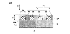
図2を参照して、領域Rは、n+ソース領域14と、p+領域18と、コンタクト電極16とを含んでいる領域である。p+領域18はn+ソース領域14と接している。コンタクト電極16は、TiSiを含む第1の領域5と、Alを含む第2の領域3を有する。第1の領域5は、主面14Aにおいてn+ソース領域14と接するn接触領域5aと、主面18Aにおいてp+領域18と接するp接触領域5bとを有している。また、第2の領域3は、n+ソース領域14およびp+領域18と接し、かつp接触領域5bおよびn接触領域5aを囲むように形成されている。
Referring to FIG. 2, region R is a region including n + source region 14, p + region 18, and
なお、第2の領域3は、Al−O結合を有する化合物を含んでいても構わない。また、コンタクト電極16は炭素を含んでいてもよく、第1の領域5および第2の領域3も炭素を含んでいても構わない。
Note that the
図2に示すように、第2の領域3の厚みは第1の領域5の厚みよりも大きく、第2の領域3が第1の領域5を覆うように形成されていても構わない。p接触領域5bは、たとえばp+領域18の主面18A上に島状に配置されている。また、n接触領域5aは、たとえばn+ソース領域14の主面14A上に島状に配置されている。p接触領域5bおよびn接触領域5aの各々の幅W(より詳細には、p接触領域5bおよびn接触領域5aの各々の炭化珪素基板10の第2の主面12Bと平行な方向における幅)は500nm以下である。好ましくは、当該幅Wは10nm以上100nm以下であり、より好ましくは、当該幅Wは30nm以上60nm以下である。なお、n+ソース領域14およびp+領域18の幅は、たとえばそれぞれ3.2μm程度および1.8μm程度である。また、コンタクト電極16の厚みTは、たとえば100nm程度である。なお、図2は、図3の線分II−IIにおける断面図である。
As shown in FIG. 2, the thickness of the
図3は、図2に示した領域Rを紙面の上側(矢印Xの方向)から見た平面図である。図3に示すように、複数のn接触領域5aはn+ソース領域14の主面14A上にまだらに配置されている。また、複数のp接触領域5bはp+領域18の主面18A上にまだらに配置されている。n+ソース領域14はp+領域18と境界2において接している。第1の領域5は、境界2においてn+ソース領域14およびp+領域18の双方に接する第1のpn接触領域5cを有していても構わない。また、コンタクト電極16は、TiCを含む第3の領域6を有していても構わない。p接触領域5b、n接触領域5a、第1のpn接触領域5cおよび第3の領域6は、平面視においてたとえば略円形を有している。
FIG. 3 is a plan view of the region R shown in FIG. 2 as viewed from the upper side of the paper (in the direction of the arrow X). As shown in FIG. 3, the plurality of
図4を参照して、第1の領域5の高さが第2の領域3の高さよりも大きくても構わない。この場合、第2の領域3の上部は第1の領域から突き出るように配置されている。なお、平面視において第2の領域3は、第1の領域5を囲むように形成されている。
Referring to FIG. 4, the height of
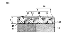
図5を参照して、複数の第1の領域5の高さが異なっていても構わない。複数の第1の領域5のうち、一方の第1の領域5の高さは第2の領域3の高さよりも大きく、他方の第1の領域5の高さは第2の領域の高さよりも小さくても構わない。具体的には、複数のp接触領域5bは、第2の領域3よりも高いp接触領域5bおよび第2の領域3よりも低いp接触領域5bを有していても構わない。同様に、複数のn接触領域5aは、第2の領域3よりも高いn接触領域5aおよび第2の領域3よりも低いn接触領域5aを有していても構わない。なお、平面視において第2の領域3は、第1の領域5を囲むように形成されている。
Referring to FIG. 5, the heights of the plurality of
図12を参照して、コンタクト電極16における原子濃度の分布について説明する。図12において左側が保護電極19側(言い換えればコンタクト電極16の表面16A側)であり、右側が炭化珪素基板10側(言い換えればコンタクト電極の裏面16B側)である。たとえばオージェ電子分光法などによってコンタクト電極16を形成する原子の濃度を分析すると、コンタクト電極16の表面16A側においてはSi(シリコン)およびC(炭素)よりもAl(アルミニウム)およびO(酸素)が多く存在する。しかしながら、コンタクト電極16の裏面16B側においては、SiおよびCがAlおよびOよりも多く存在する。
With reference to FIG. 12, the atomic concentration distribution in the
好ましくは、コンタクト電極16の裏面16B側において、C(炭素)の原子数が、Si(シリコン)の原子数よりも多い領域Sが存在する。C(炭素)の原子数が、Si(シリコン)の原子数よりも多い領域Sが存在するコンタクト電極16は、C(炭素)の原子数が、Si(シリコン)の原子数よりも多い領域Sが存在しないコンタクト電極16よりも低い接触抵抗を示す。
Preferably, on the back surface 16B side of the
好ましくは、コンタクト電極16における、Ti(チタン)の原子数をx、Al(アルミニウム)の原子数をy、Si(シリコン)の原子数をzとしたとき、x、yおよびzのうち任意の2つの原子数の比は1/3以上3以下である。つまり、原子の数が多い原子の数を原子の数が少ない原子の数で除した値は3以下であり、原子の数が少ない原子の数を原子の数が多い原子の数で除した値は1/3以上である。たとえば、Tiの原子数はSiの原子数の1/3倍以上3倍以下であり、Siの原子数はAlの原子数の1/3倍以上3倍以下であり、Alの原子数はTiの原子数の1/3倍以上3倍以下である。
Preferably, in the
次にMOSFET1の動作について説明する。ゲート電極17に閾値以下の電圧を与えた状態、すなわちオフ状態では、ゲート酸化膜15の直下に位置するpボディ13とn-SiC層12との間が逆バイアスとなり、非導通状態となる。一方、ゲート電極17に正の電圧を印加していくと、pボディ13のゲート酸化膜15と接触する付近であるチャネル領域13Aにおいて、反転層が形成される。その結果、n+ソース領域14とn-SiC層12とが電気的に接続され、ソース電極22とドレイン電極20との間に電流が流れる。
Next, the operation of
次に、実施の形態1における炭化珪素半導体装置としてのMOSFET1の製造方法について説明する。
Next, a method for manufacturing
図7および図8を参照して、まず基板準備工程S10(図6)によって炭化珪素基板10が準備される。
Referring to FIGS. 7 and 8, first,
具体的には、まずn+SiC基板11上におけるエピタキシャル成長により、n+SiC基板11の一方の主面11A上にn-SiC層12が形成される。エピタキシャル成長は、たとえば原料ガスとしてSiH4(シラン)とC3H8(プロパン)との混合ガスを採用して実施することができる。このとき、n型不純物として、たとえばN(窒素)を導入する。これにより、n+SiC基板11に含まれるn型不純物よりも低い濃度のn型不純物を含むn-SiC層12を形成することができる。
Specifically, the first epitaxial growth on n + SiC substrate 11, n on one
次に第2の主面12B上に、たとえばCVD(Chemical Vapor Deposition;化学蒸着法)によりSiO2からなる酸化膜が形成される。そして、酸化膜の上にレジストが塗布された後、露光および現像が行なわれ、所望のpボディ13の形状に応じた領域に開口を有するレジスト膜が形成される。そして、当該レジスト膜をマスクとして用いて、たとえばRIE(Reactive Ion Etching;反応性イオンエッチング)により酸化膜が部分的に除去されることによって、n-SiC層12上に開口パタ-ンを有する酸化膜からなるマスク層が形成される。その後、上記レジスト膜を除去した上で、このマスク層をマスクとして用いて、Alなどのp型不純物をn-SiC層12にイオン注入することにより、n-SiC層12にpボディ13が形成される。
Next, an oxide film made of SiO 2 is formed on second
次に、マスクとして使用された上記酸化膜が除去された上で、所望のn+ソース領域14の形状に応じた領域に開口を有するマスク層が形成される。そして、このマスク層をマスクとして用いて、P(リン)などのn型不純物がn-SiC層12にイオン注入により導入されることによりn+ソース領域14が形成される。次に、所望のp+領域18の形状に応じた領域に開口を有するマスク層が形成され、これをマスクとして用いて、Al、Bなどのp型不純物がn-SiC層12にイオン注入により導入されることによりp+領域18が形成される。 Next, after removing the oxide film used as a mask, a mask layer having an opening in a region corresponding to the shape of the desired n + source region 14 is formed. Then, using this mask layer as a mask, an n + source region 14 is formed by introducing an n-type impurity such as P (phosphorus) into the n − SiC layer 12 by ion implantation. Next, a mask layer having an opening in a region corresponding to the shape of the desired p + region 18 is formed. Using this as a mask, p-type impurities such as Al and B are ion-implanted into the n − SiC layer 12. By introducing, p + region 18 is formed.
次に、上記イオン注入によって導入された不純物を活性化させる熱処理が実施される。具体的には、イオン注入が実施されたn-SiC層12が、たとえばAr(アルゴン)雰囲気中において1700℃程度に加熱され、30分間程度保持される。以上により、第2の主面12Bを有する炭化珪素基板10(図8)が準備される。
Next, heat treatment for activating the impurities introduced by the ion implantation is performed. Specifically, the n − SiC layer 12 subjected to ion implantation is heated to about 1700 ° C. in, for example, an Ar (argon) atmosphere and is held for about 30 minutes. Thus, silicon carbide substrate 10 (FIG. 8) having second
図9を参照して、ゲート絶縁膜形成工程S20(図6)によって、ゲート酸化膜15(絶縁膜)が形成される。具体的には、まず、上記工程が実施されて所望のイオン注入領域を含むn-SiC層12が形成されたn+基板11が熱酸化される。熱酸化は、たとえば酸素雰囲気中で1300℃程度に加熱し、40分間程度保持することにより実施することができる。これにより第2の主面12B上に、二酸化珪素(SiO2)からなる熱酸化膜15A(たとえば厚み50nm程度)が形成される。
Referring to FIG. 9, gate oxide film 15 (insulating film) is formed by gate insulating film forming step S20 (FIG. 6). Specifically, first, the n + substrate 11 on which the n − SiC layer 12 including the desired ion implantation region is formed by the above process is thermally oxidized. Thermal oxidation can be carried out, for example, by heating to about 1300 ° C. in an oxygen atmosphere and holding for about 40 minutes. As a result, a
次に、熱酸化膜15A上にレジストが塗布された後、露光および現像が行なわれ、コンタクト電極16(図1参照)を形成すべき領域に応じた開口を有するレジスト膜が形成される。そして、当該レジスト膜をマスクとして用いて、たとえばRIEにより熱酸化膜が部分的に除去される。これにより、第2の主面12Bの一部を覆うゲート酸化膜15が形成される。
Next, after applying a resist on
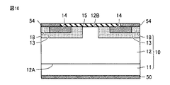
図10を参照して、コンタクト電極形成工程S30(図6)が行われる。
具体的には、たとえば、Ti部、Al部およびSi部が炭化珪素基板10上に順に積層された金属層54がn+ソース領域14およびp+領域18上に形成される。Ti部、Al部およびSi部の厚みは、たとえばそれぞれ250Å、200Åおよび300Åである。好ましくは、金属層54の厚みは1μm以下であり、より好ましくは500nm以下であり、さらに好ましくは100nm以下である。金属層54の厚みが薄い方が合金化が早く行われる。好ましくは、金属層54の形成はスパッタ法または蒸着法によって行なわれる。
Referring to FIG. 10, contact electrode formation step S30 (FIG. 6) is performed.
Specifically, for example, a
また、当該金属層54は、Ti部、Al部およびSi部が炭化珪素基板10の第2の主面12Bと平行な方向に配列された並列構造であってもよいし、格子状に配列された構造であってもよい。また、金属層54はTi部、Al部およびSi部が混合されて形成された混合膜であってもよい。
Further, the
次にレジスト膜が除去されることにより、レジスト膜上の金属層54が除去(リフトオフ)されて、n+ソース領域14およびp+領域18に接する金属層54が残される。
Next, by removing the resist film, the
図11を参照して、金属層54形成後、アニール工程において、金属層54を加熱することによって金属層54が合金化され、炭化珪素基板10とオーミック接触するコンタクト電極16が形成される。具体的には、Arなどの不活性ガス雰囲気中において、金属層54および炭化珪素基板10は、たとえば950℃以上1200℃以下の温度、たとえば1000℃に加熱され、たとえば30秒以上300秒以下の間保持される。これにより、金属層54に含まれていた、TiとSiとが凝集して島状となり、TiSiを含む第1の領域5となる。また、Alは第1の層を囲むよう広がり、Alを含む第2の領域3が形成される。このようにして、TiSiを含む第1の領域5と、Alを含む第2の領域3とがまだらに混在して形成されたコンタクト電極16となる。なお、上記のような構成を有するコンタクト電極16を形成するためには、アニール時間を長くすることが好ましい。たとえば、金属層54および炭化珪素基板10は、たとえば950℃以上1200℃以下の温度、たとえば1000℃に加熱され、たとえば120秒以上150秒以下の間保持される。
Referring to FIG. 11, after formation of
次にドレイン電極形成工程S40(図6)によってドレイン電極20が炭化珪素基板10の第2の主面12Bとは反対側の面に形成される。たとえば、NiをスパッタリングしてNi層を当該反対側の面に形成し、当該Ni層をアニールすることによりドレイン電極20が形成される。なお、当該Ni層の代わりに上述した金属層54が用いられても構わない。
Next,
再び図1を参照して、ゲート電極形成工程S50(図6)によってゲート電極17が形成される。この工程では、たとえば導電体であるポリシリコン、Alなどからなるゲート電極17が、一方のn+ソース領域14上から他方のn+ソース領域14上にまで延在するとともに、ゲート酸化膜15に接触するように形成される。ゲート電極の素材としてポリシリコンを採用する場合、当該ポリシリコンは、P(リン)が1×1020cm-3を超える高い濃度で含まれるものとすることができる。
Referring to FIG. 1 again,
次に保護電極形成工程S60(図6)によって保護電極19が形成される。この工程では、たとえば蒸着法により、導電体であるAlからなる保護電極19が、コンタクト電極16の表面16A上に形成される。これによりソース電極22が完成する。
Next, the
次にパシベーション膜形成工程S70(図6)によってパシベーション膜21が形成される。この工程では、一方の保護電極19上からゲート電極17上を通り、他方の保護電極19上にまで延在するように、たとえばSiO2からなるこのパシベーション膜21が形成される。このパシベーション膜21は、たとえばCVD法により形成することができる。以上によりMOSFET1が完成する。
Next, the
なお上記実施の形態におけるn型とp型とが入れ替えられた構成が用いられてもよい。また上記においては、本発明の炭化珪素半導体装置の一例として、プレーナ型のMOSFETについて説明したがこれに限られない。たとえば、炭化珪素半導体装置は、たとえばトレンチ型のMOSFETやIGBT(Insulated Gate Bipolar Transistor、絶縁ゲートバイポ-ラトランジスタ)などであっても構わない。 Note that a configuration in which the n-type and the p-type in the above embodiment are interchanged may be used. In the above description, a planar MOSFET has been described as an example of the silicon carbide semiconductor device of the present invention, but the present invention is not limited to this. For example, the silicon carbide semiconductor device may be, for example, a trench type MOSFET or an IGBT (Insulated Gate Bipolar Transistor).
次に、本実施の形態の作用効果について説明する。
本実施の形態に係るMOSFET1によれば、TiSiを含むn接触領域5aはn+ソース領域14に接触し、Alを含む第2の領域3はp+領域18に接触している。これにより、TiSiを含むn接触領域5aとn+ソース領域14とにおいてオーミック接触が可能であり、かつAlを含む第2の領域3とp+領域18とにおいてオーミック接触が可能である。結果として、n+ソース領域14およびp+領域18の双方に対してオーミック接触を実現することができる。
Next, the effect of this Embodiment is demonstrated.
According to
また本実施の形態に係るMOSFET1によれば、コンタクト電極16は、炭素の原子数がシリコンの原子数よりも多い領域を含む。これにより、炭素の原子数がシリコンの原子数よりも多い領域を含まないコンタクト電極16と比較して、低い接触抵抗を実現することができる。
According to
さらに本実施の形態に係るMOSFET1によれば、第2の領域3は、p接触領域5bとn接触領域5aとを覆うように形成されている。これにより、保護電極19に対向する第2の領域3の面積が大きくなるため、保護電極19との密着性を向上することができる。
Furthermore, according to
さらに本実施の形態に係るMOSFET1によれば、コンタクト電極16における、Tiの原子数をx、Alの原子数をy、Siの原子数をzとしたとき、x、yおよびzのうち任意の2つの原子数の比は1/3以上3以下である。これにより、n型領域およびp型領域の双方に対して良好なオーミック接触を実現することができる。
Furthermore, according to
さらに本実施の形態に係るMOSFET1によれば、p接触領域5bおよびn接触領域5aの各々の炭化珪素基板10の第2の主面12Bと平行な方向における幅Wは500nm以下である。これにより、n+ソース領域14およびp+領域18の双方に対して良好なオーミック接触を実現することができる。
Furthermore, according to
さらに本実施の形態に係るMOSFET1によれば、コンタクト電極16は、TiCを含む第3の領域6をさらに有するので、n+ソース領域14およびp+領域18の双方に対してより良好なオーミック接触を実現することができる。
Furthermore, according to
今回開示された実施の形態はすべての点で例示であって、制限的なものではないと考えられるべきである。本発明の範囲は上記した説明ではなくて特許請求の範囲によって示され、特許請求の範囲と均等の意味、および範囲内でのすべての変更が含まれることが意図される。 The embodiment disclosed this time is to be considered as illustrative in all points and not restrictive. The scope of the present invention is defined by the terms of the claims, rather than the description above, and is intended to include any modifications within the scope and meaning equivalent to the terms of the claims.
1 MOSFET(炭化珪素半導体装置)、3 第2の領域、5 第1の領域、5a n接触領域、5b p接触領域、6 第3の領域、10 炭化珪素基板、11 n+基板、12 n-SiC層、12B 第2の主面、13 pボディ、13A チャネル領域、14 n+ソース領域、15 ゲート酸化膜(絶縁膜)、15A 熱酸化膜、16 コンタクト電極、17 ゲート電極、18 p+領域、19 保護電極、20 ドレイン電極、21 パシベーション膜、22 ソース電極、54 金属層。
DESCRIPTION OF
Claims (6)
前記炭化珪素基板と接するコンタクト電極とを備え、
前記コンタクト電極は、TiSiを含む第1の領域と、Alを含む第2の領域とを有し、
前記第1の領域は、前記n型領域と接するn接触領域と、前記p型領域と接するp接触領域とを有し、
前記第2の領域は、前記p型領域および前記n型領域と接し、かつ前記p接触領域および前記n接触領域を囲むように形成されている、炭化珪素半導体装置。 a silicon carbide substrate including an n-type region and a p-type region in contact with the n-type region;
A contact electrode in contact with the silicon carbide substrate,
The contact electrode has a first region containing TiSi and a second region containing Al,
The first region has an n contact region in contact with the n type region, and a p contact region in contact with the p type region,
The silicon carbide semiconductor device, wherein the second region is formed to contact the p-type region and the n-type region and surround the p-contact region and the n-contact region.
Priority Applications (5)
| Application Number | Priority Date | Filing Date | Title |
|---|---|---|---|
| JP2012139386A JP2014003253A (en) | 2012-06-21 | 2012-06-21 | Silicon carbide semiconductor device |
| EP13807640.1A EP2866263A4 (en) | 2012-06-21 | 2013-04-25 | Silicon carbide semiconductor device |
| PCT/JP2013/062210 WO2013190907A1 (en) | 2012-06-21 | 2013-04-25 | Silicon carbide semiconductor device |
| CN201380024867.4A CN104285299A (en) | 2012-06-21 | 2013-04-25 | Silicon carbide semiconductor device |
| US13/895,910 US8729567B2 (en) | 2012-06-21 | 2013-05-16 | Silicon carbide semiconductor device |
Applications Claiming Priority (1)
| Application Number | Priority Date | Filing Date | Title |
|---|---|---|---|
| JP2012139386A JP2014003253A (en) | 2012-06-21 | 2012-06-21 | Silicon carbide semiconductor device |
Publications (1)
| Publication Number | Publication Date |
|---|---|
| JP2014003253A true JP2014003253A (en) | 2014-01-09 |
Family
ID=49768514
Family Applications (1)
| Application Number | Title | Priority Date | Filing Date |
|---|---|---|---|
| JP2012139386A Withdrawn JP2014003253A (en) | 2012-06-21 | 2012-06-21 | Silicon carbide semiconductor device |
Country Status (5)
| Country | Link |
|---|---|
| US (1) | US8729567B2 (en) |
| EP (1) | EP2866263A4 (en) |
| JP (1) | JP2014003253A (en) |
| CN (1) | CN104285299A (en) |
| WO (1) | WO2013190907A1 (en) |
Families Citing this family (3)
| Publication number | Priority date | Publication date | Assignee | Title |
|---|---|---|---|---|
| JP2014003253A (en) * | 2012-06-21 | 2014-01-09 | Sumitomo Electric Ind Ltd | Silicon carbide semiconductor device |
| JP6922202B2 (en) | 2016-12-07 | 2021-08-18 | 富士電機株式会社 | Semiconductor devices and methods for manufacturing semiconductor devices |
| DE102016125030A1 (en) | 2016-12-20 | 2018-06-21 | Infineon Technologies Ag | Forming a metal contact layer on silicon carbide and semiconductor device having a metal contact structure |
Family Cites Families (11)
| Publication number | Priority date | Publication date | Assignee | Title |
|---|---|---|---|---|
| US7217954B2 (en) | 2003-03-18 | 2007-05-15 | Matsushita Electric Industrial Co., Ltd. | Silicon carbide semiconductor device and method for fabricating the same |
| JP3759145B2 (en) * | 2003-03-18 | 2006-03-22 | 松下電器産業株式会社 | Silicon carbide semiconductor device and manufacturing method thereof |
| JP2006332199A (en) * | 2005-05-24 | 2006-12-07 | Shindengen Electric Mfg Co Ltd | SiC SEMICONDUCTOR DEVICE |
| JPWO2008018342A1 (en) * | 2006-08-09 | 2009-12-24 | 独立行政法人産業技術総合研究所 | Silicon carbide semiconductor device and manufacturing method thereof |
| JP4960125B2 (en) * | 2007-03-22 | 2012-06-27 | 株式会社東芝 | Semiconductor device and manufacturing method thereof |
| US8373176B2 (en) * | 2008-04-15 | 2013-02-12 | Sumitomo Electric Industries, Ltd. | Semiconductor device and method of manufacturing the same |
| JP5668414B2 (en) * | 2010-11-01 | 2015-02-12 | 住友電気工業株式会社 | Manufacturing method of semiconductor device |
| JP2012253293A (en) * | 2011-06-07 | 2012-12-20 | Sumitomo Electric Ind Ltd | Semiconductor device |
| JP5728339B2 (en) * | 2011-09-08 | 2015-06-03 | 株式会社東芝 | Semiconductor device and manufacturing method of semiconductor device |
| JP5646527B2 (en) * | 2012-03-02 | 2014-12-24 | 株式会社東芝 | Semiconductor device and manufacturing method of semiconductor device |
| JP2014003253A (en) * | 2012-06-21 | 2014-01-09 | Sumitomo Electric Ind Ltd | Silicon carbide semiconductor device |
-
2012
- 2012-06-21 JP JP2012139386A patent/JP2014003253A/en not_active Withdrawn
-
2013
- 2013-04-25 WO PCT/JP2013/062210 patent/WO2013190907A1/en active Application Filing
- 2013-04-25 EP EP13807640.1A patent/EP2866263A4/en not_active Withdrawn
- 2013-04-25 CN CN201380024867.4A patent/CN104285299A/en active Pending
- 2013-05-16 US US13/895,910 patent/US8729567B2/en active Active
Also Published As
| Publication number | Publication date |
|---|---|
| US8729567B2 (en) | 2014-05-20 |
| EP2866263A4 (en) | 2016-02-10 |
| WO2013190907A1 (en) | 2013-12-27 |
| US20130341647A1 (en) | 2013-12-26 |
| CN104285299A (en) | 2015-01-14 |
| EP2866263A1 (en) | 2015-04-29 |
Similar Documents
| Publication | Publication Date | Title |
|---|---|---|
| JP5525940B2 (en) | Semiconductor device and manufacturing method of semiconductor device | |
| WO2014112204A1 (en) | Silicon carbide semiconductor device | |
| WO2010116575A1 (en) | Semiconductor device and method of producing semiconductor device | |
| JP5577478B1 (en) | Semiconductor device | |
| JP5668414B2 (en) | Manufacturing method of semiconductor device | |
| JP5728954B2 (en) | Method for manufacturing silicon carbide semiconductor device | |
| WO2012032735A1 (en) | Semiconductor device and process for production thereof | |
| KR20100100585A (en) | Method of producing semiconductor device and semiconductor device | |
| WO2012165008A1 (en) | Silicon carbide semiconductor device and method for manufacturing same | |
| WO2014083943A1 (en) | Silicon carbide semiconductor device, and manufacturing method for same | |
| JP6208106B2 (en) | Semiconductor device and manufacturing method thereof | |
| JP2015156429A (en) | Silicon carbide semiconductor device and manufacturing method of the same | |
| WO2013190907A1 (en) | Silicon carbide semiconductor device | |
| JP6295797B2 (en) | Silicon carbide semiconductor device and manufacturing method thereof | |
| WO2014027518A1 (en) | Silicon-carbide semiconductor device and manufacturing method therefor | |
| WO2013094328A1 (en) | Semiconductor device and method for producing same | |
| TW201310546A (en) | Method for manufacturing semiconductor device | |
| JP5949305B2 (en) | Method for manufacturing silicon carbide semiconductor device | |
| JPWO2019198168A1 (en) | Manufacturing method of semiconductor devices and semiconductor devices | |
| JP2017147471A (en) | Semiconductor device | |
| WO2013190901A1 (en) | Silicon carbide semiconductor device and method for producing same | |
| JP2016058661A (en) | Semiconductor device | |
| JP5602256B2 (en) | Manufacturing method of semiconductor device | |
| JP5991629B2 (en) | Semiconductor device and manufacturing method of semiconductor device | |
| US20160133707A1 (en) | Silicon carbide semiconductor device and method for manufacturing same |
Legal Events
| Date | Code | Title | Description |
|---|---|---|---|
| A621 | Written request for application examination |
Free format text: JAPANESE INTERMEDIATE CODE: A621 Effective date: 20150224 |
|
| A761 | Written withdrawal of application |
Free format text: JAPANESE INTERMEDIATE CODE: A761 Effective date: 20160401 |