EP2865028B1 - Large area organic photovoltaics - Google Patents
Large area organic photovoltaics Download PDFInfo
- Publication number
- EP2865028B1 EP2865028B1 EP13739878.0A EP13739878A EP2865028B1 EP 2865028 B1 EP2865028 B1 EP 2865028B1 EP 13739878 A EP13739878 A EP 13739878A EP 2865028 B1 EP2865028 B1 EP 2865028B1
- Authority
- EP
- European Patent Office
- Prior art keywords
- cleaning
- layer
- stream
- substrate
- devices
- Prior art date
- Legal status (The legal status is an assumption and is not a legal conclusion. Google has not performed a legal analysis and makes no representation as to the accuracy of the status listed.)
- Active
Links
Images




Classifications
-
- H—ELECTRICITY
- H10—SEMICONDUCTOR DEVICES; ELECTRIC SOLID-STATE DEVICES NOT OTHERWISE PROVIDED FOR
- H10K—ORGANIC ELECTRIC SOLID-STATE DEVICES
- H10K71/00—Manufacture or treatment specially adapted for the organic devices covered by this subclass
-
- H—ELECTRICITY
- H10—SEMICONDUCTOR DEVICES; ELECTRIC SOLID-STATE DEVICES NOT OTHERWISE PROVIDED FOR
- H10K—ORGANIC ELECTRIC SOLID-STATE DEVICES
- H10K30/00—Organic devices sensitive to infrared radiation, light, electromagnetic radiation of shorter wavelength or corpuscular radiation
- H10K30/20—Organic devices sensitive to infrared radiation, light, electromagnetic radiation of shorter wavelength or corpuscular radiation comprising organic-organic junctions, e.g. donor-acceptor junctions
-
- B—PERFORMING OPERATIONS; TRANSPORTING
- B82—NANOTECHNOLOGY
- B82Y—SPECIFIC USES OR APPLICATIONS OF NANOSTRUCTURES; MEASUREMENT OR ANALYSIS OF NANOSTRUCTURES; MANUFACTURE OR TREATMENT OF NANOSTRUCTURES
- B82Y10/00—Nanotechnology for information processing, storage or transmission, e.g. quantum computing or single electron logic
-
- H—ELECTRICITY
- H10—SEMICONDUCTOR DEVICES; ELECTRIC SOLID-STATE DEVICES NOT OTHERWISE PROVIDED FOR
- H10K—ORGANIC ELECTRIC SOLID-STATE DEVICES
- H10K30/00—Organic devices sensitive to infrared radiation, light, electromagnetic radiation of shorter wavelength or corpuscular radiation
- H10K30/80—Constructional details
- H10K30/81—Electrodes
-
- H—ELECTRICITY
- H10—SEMICONDUCTOR DEVICES; ELECTRIC SOLID-STATE DEVICES NOT OTHERWISE PROVIDED FOR
- H10K—ORGANIC ELECTRIC SOLID-STATE DEVICES
- H10K71/00—Manufacture or treatment specially adapted for the organic devices covered by this subclass
- H10K71/10—Deposition of organic active material
-
- H—ELECTRICITY
- H10—SEMICONDUCTOR DEVICES; ELECTRIC SOLID-STATE DEVICES NOT OTHERWISE PROVIDED FOR
- H10K—ORGANIC ELECTRIC SOLID-STATE DEVICES
- H10K77/00—Constructional details of devices covered by this subclass and not covered by groups H10K10/80, H10K30/80, H10K50/80 or H10K59/80
- H10K77/10—Substrates, e.g. flexible substrates
-
- H—ELECTRICITY
- H10—SEMICONDUCTOR DEVICES; ELECTRIC SOLID-STATE DEVICES NOT OTHERWISE PROVIDED FOR
- H10K—ORGANIC ELECTRIC SOLID-STATE DEVICES
- H10K85/00—Organic materials used in the body or electrodes of devices covered by this subclass
- H10K85/20—Carbon compounds, e.g. carbon nanotubes or fullerenes
- H10K85/211—Fullerenes, e.g. C60
-
- H—ELECTRICITY
- H10—SEMICONDUCTOR DEVICES; ELECTRIC SOLID-STATE DEVICES NOT OTHERWISE PROVIDED FOR
- H10K—ORGANIC ELECTRIC SOLID-STATE DEVICES
- H10K2102/00—Constructional details relating to the organic devices covered by this subclass
-
- H—ELECTRICITY
- H10—SEMICONDUCTOR DEVICES; ELECTRIC SOLID-STATE DEVICES NOT OTHERWISE PROVIDED FOR
- H10K—ORGANIC ELECTRIC SOLID-STATE DEVICES
- H10K30/00—Organic devices sensitive to infrared radiation, light, electromagnetic radiation of shorter wavelength or corpuscular radiation
- H10K30/50—Photovoltaic [PV] devices
-
- Y—GENERAL TAGGING OF NEW TECHNOLOGICAL DEVELOPMENTS; GENERAL TAGGING OF CROSS-SECTIONAL TECHNOLOGIES SPANNING OVER SEVERAL SECTIONS OF THE IPC; TECHNICAL SUBJECTS COVERED BY FORMER USPC CROSS-REFERENCE ART COLLECTIONS [XRACs] AND DIGESTS
- Y02—TECHNOLOGIES OR APPLICATIONS FOR MITIGATION OR ADAPTATION AGAINST CLIMATE CHANGE
- Y02E—REDUCTION OF GREENHOUSE GAS [GHG] EMISSIONS, RELATED TO ENERGY GENERATION, TRANSMISSION OR DISTRIBUTION
- Y02E10/00—Energy generation through renewable energy sources
- Y02E10/50—Photovoltaic [PV] energy
- Y02E10/549—Organic PV cells
-
- Y—GENERAL TAGGING OF NEW TECHNOLOGICAL DEVELOPMENTS; GENERAL TAGGING OF CROSS-SECTIONAL TECHNOLOGIES SPANNING OVER SEVERAL SECTIONS OF THE IPC; TECHNICAL SUBJECTS COVERED BY FORMER USPC CROSS-REFERENCE ART COLLECTIONS [XRACs] AND DIGESTS
- Y02—TECHNOLOGIES OR APPLICATIONS FOR MITIGATION OR ADAPTATION AGAINST CLIMATE CHANGE
- Y02P—CLIMATE CHANGE MITIGATION TECHNOLOGIES IN THE PRODUCTION OR PROCESSING OF GOODS
- Y02P70/00—Climate change mitigation technologies in the production process for final industrial or consumer products
- Y02P70/50—Manufacturing or production processes characterised by the final manufactured product
Definitions
- the subject matter of the present disclosure was made by, on behalf of, and/or in connection with one or more of the following parties to a joint university-corporation research agreement: University of Michigan and Global Photonic Energy Corporation.
- the agreement was in effect on and before the date the subject matter of the present disclosure was prepared, and was made as a result of activities undertaken within the scope of the agreement.
- the present disclosure generally relates to methods of making organic photovoltaic (OPV) devices, such as solar cells, through the use of large areas of organic molecular layers.
- OCV organic photovoltaic
- Photosensitive optoelectronic devices convert electromagnetic radiation into electricity.
- Solar cells are a type of photosensitive optoelectronic device that are specifically used to generate electrical power.
- n-type denotes that the majority carrier type is the electron. This could be viewed as the material having many electrons in relatively free energy states.
- p-type denotes that the majority carrier type is the hole. Such material has many holes in relatively free energy states.
- the type of the background, i.e., not photo-generated, majority carrier concentration depends primarily on unintentional doping by defects or impurities.
- the type and concentration of impurities determine the value of the Fermi energy, or level, within the gap between the conduction band minimum and valance band maximum energies.
- the Fermi energy characterizes the statistical occupation of molecular quantum energy states denoted by the value of energy for which the probability of occupation is equal to 1/2.
- a Fermi energy near the conduction band minimum energy indicates that electrons are the predominant carrier.
- a Fermi energy near the valence band maximum energy indicates that holes are the predominant carrier. Accordingly, the Fermi energy is a primary characterizing property of traditional semiconductors and the prototypical PV junction has traditionally been the p-n interface.
- OPV devices are a promising renewable and green energy source because of their potential for low cost solar energy conversion.
- an organic material suitable for an optical device When an organic material suitable for an optical device is irradiated with appropriate light a photon is absorbed by a molecular component of the material and, as a result, an excited state of the molecular component is produced: an electron is promoted from the HOMO (highest occupied molecular orbital) state to the LUMO (lowest unoccupied molecular orbital) state of the molecule, or a hole is promoted from the LUMO to the HOMO.
- an exciton i.e. an electron-hole pair state is generated. This exciton state has a natural life-time before the electron and the hole will recombine. In order to create a photocurrent the components of the electron-hole pair have to be separated.
- the separation can be achieved by juxtaposing two layers of materials with different conductive properties.
- the interface between the layers forms a photovoltaic heterojunction and it should have an asymmetric conduction characteristic, i.e., it should be capable of supporting electronic charge transport preferably in one direction.
- Li et al., Proc. SPIE., vol. 6722, p. 672241 (2007 ) describes cleaning of ITO glass with carbon dioxide snow jet spray.
- Li et al., Proc. SPIE, vol. 7282, p. 72822K (2009 ) describes ITO glass polishing using carbon dioxide snow jet technique for organic light-emitting diodes.
- WO 2011/152091 A1 describes an electrode foil which serves as both a supporting base and a reflective electrode, and an organic device which uses the electrode foil.
- the electrode foil comprises a metal foil and a reflective layer that is provided directly on the metal foil. Prior to the formation of the reflective layer on the metal foil particles on an ultra-smooth surface of the metal foil may be removed using a dry-ice blasting method.
- the present disclosure is directed to a process for manufacturing a photovoltaic device according to claim 1.
- the term “layer” refers to a member or component of a photosensitive device whose primary dimension is X-Y, i.e., along its length and width, and is typically perpendicular to the plane of incidence of the illumination. It should be understood that the term “layer” is not necessarily limited to single layers or sheets of materials. A layer can comprise laminates or combinations of several sheets of materials. In addition, it should be understood that the surfaces of certain layers, including the interface(s) of such layers with other material(s) or layers(s), may be imperfect, wherein said surfaces represent an interpenetrating, entangled or convoluted network with other material(s) or layer(s). Similarly, it should also be understood that a layer may be discontinuous, such that the continuity of said layer along the X-Y dimension may be disturbed or otherwise interrupted by other layer(s) or material(s).
- the expression “disposed on” permits other materials or layers to exist between a disposed material and the material on which it is disposed.
- the expression “deposited on” permits other materials or layers to exist between a deposited material and the material on which it is deposited.
- other materials or layers may exist between a surface of a substrate and a material "disposed on” or “deposited on” the surface of the substrate.
- yield refers to the proportion of devices, made or manufactured by a process, that performs within a given range of specifications.
- exposing the surface of a substrate to a stream of at least one compound comprising one or more phases chosen from supercritical, gaseous, solid, and liquid phases permits the manufacture of large area solar devices having thin organic layers, e.g., a total deposited thickness of ⁇ 70 nm, without compromising, and even increasing, yield.
- the substrate is an ITO-coated substrate.
- the process of the present disclosure provides a multi-layer solar device comprising a substrate, and an active area comprising at least one donor material and at least one acceptor material deposited on a surface of the substrate, wherein the donor and acceptor materials are comprised of organic molecules, and wherein particulates are removed from the surface of the substrate before deposition of the donor and acceptor materials.
- the process of the present disclosure provides a multi-layer solar device comprising a pre-cleaned substrate having a surface substantially free of particulates, and an active layer comprising at least one donor material and at least one acceptor material disposed on the surface of the substrate, wherein the donor and acceptor materials are comprised of organic molecules.
- the surface of the substrate comprises an electrode, such as an anode or cathode.
- the process of the present disclosure provides a multi-layer solar device comprising a pre-cleaned substrate having a surface substantially free of particulates, two electrodes in superposed relation disposed on the surface of the pre-cleaned substrate, and an active area comprising at least one donor material and at least one acceptor material, wherein the donor and acceptor materials are comprised of organic molecules located between the two electrodes.
- the particulates are removed by exposing the surface of the substrate to a stream of at least one compound comprising one or more phases chosen from supercritical, gaseous, solid, and liquid phases. This process is referred to herein as "snow cleaning.” A substrate is pre-cleaned by snow cleaning.
- the stream of the at least one compound contains at least gaseous and solid phases. In certain embodiments, the stream of the at least one compound contains gaseous, solid, and liquid phases. In certain embodiments, the stream of the at least one compound comprises a supercritical fluid.
- the exposure to the stream of the at least one compound is via directed flow.
- the at least one compound used to remove particulates comprises CO 2 .
- This process of CO 2 based cleaning is referred to as CO 2 snow cleaning, or CO 2 cleaning.
- CO 2 snow cleaning is nondestructive, nonabrasive, residue-free, and environmentally friendly.
- a compound in addition to, CO 2 is selected and used in a manner as described herein.
- the molecule chosen could be selected based on solvation properties for a particular contaminate, or chosen to create a stream containing one or more phases chosen from gas, liquid, solid and supercritical phases.
- Examples of compounds may include ammonia, nitrous oxide, various hydrocarbons such as acetylene, propane, butane or other hydrocarbons, various chlorinated hydrocarbons such as chloroethanes, various fluorinated hydrocarbons such as fluoroethanes, or mixtures thereof.
- Exemplary compounds include those that form a liquid or solid upon cooling below room temperature.
- snow-cleaned substrates are prepared by exposing a surface of the substrate to CO 2 around its triple point, i.e., in various parts of the stream, gas, liquid, and solid phases are present.
- snow cleaning relies on the expansion of a liquid or gaseous compound, e.g., CO 2 , as it emerges from an orifice.
- a liquid or gaseous compound e.g., CO 2
- the resulting stream of material e.g, a combination of at least solid and gaseous phases, physically remove particulates by the momentum of the impacting solid particles and/or by the momentum of the gas, thereby overcoming the adhesional force binding particulates to the surface.
- Other residues on the substrate can be removed by dissolution of contaminates into a liquid or supercritical fluid.
- the active area of the solar device ranges from about 0.5 cm 2 to 50 cm 2 , from about 1 cm 2 to about 10 cm 2 , and from about 2.56 cm 2 to about 6.25 cm 2 . In yet another embodiment, the active area ranges from about 0.1 cm 2 to about 6.25 cm 2 .
- the active area of the solar device is a large area of at least about 0.25 cm 2 , about 0.5 cm 2 , about 1 cm 2 , about 5 cm 2 , about 6.25 cm 2 , about 10 cm 2 , or 50 cm 2 .
- Removed particulates may vary in size. In some embodiments, particulates that are removed range in diameter from about 5 nm to about 1000 nm, from about 15 nm to about 200 nm, from about 20 nm to about 100 nm, and from about 30 nm to about 60 nm.
- the organic active layer has a thickness ranging from 50 nm to 80 nm.
- the surface of the substrate is cleaned using a technique in addition to snow cleaning, wherein the additional cleaning technique is solvent cleaning.
- additional techniques include soaking in solvents such as, for example, trichloroethylene, acetone, and isopropanol.
- snow cleaning increases yield without compromising efficiency. In some embodiments, snow cleaning reduces or eliminates short circuits in the solar device.
- the present disclosure is directed to a process for manufacturing a photovoltaic device comprising, providing a substrate, cleaning a surface of the substrate by exposing the surface to a stream of at least one compound comprising one or more phases chosen from supercritical, gaseous, solid, and liquid phases, and depositing an organic active layer on the surface of the substrate.
- the surface of the substrate exposed to the stream of the at least one compound comprises an electrode, such as an anode or cathode.
- a process for manufacturing a photovoltaic device comprises, providing a first electrode layer, cleaning the first electrode layer by exposing the first electrode layer to a stream of at least one compound comprising one or more phases chosen from supercritical, gaseous, solid, and liquid phases, providing a second electrode, wherein an organic active layer is deposited between the first electrode layer and the second electrode layer.
- the present disclosure provides a process for manufacturing a photovoltaic device comprising, providing a first electrode layer, cleaning the first electrode layer by exposing the first electrode layer to a stream of at least one compound comprising one or more phases chosen from supercritical, gaseous, solid, and liquid and combinations thereof, providing a second electrode layer, depositing an organic active layer between the first electrode layer and the second electrode layer, wherein the thickness of the organic active layer is such that it improves yield over a yield obtained without cleaning the first electrode layer with the stream of the at least one compound.
- the organic active layer as used herein may comprise at least one donor material and at least one acceptor material.
- the stream of the at least one compound contains at least gaseous and solid phases. In certain embodiments, the stream of the at least one compound contains gaseous, solid, and liquid phases. In certain embodiments, the stream of the at least one compound comprises a supercritical fluid.
- the exposure to the at least one compound is via directed flow.
- the at least one compound comprises CO 2 .
- a compound in addition to CO 2 is selected and used in a manner as described herein.
- the molecule chosen could be selected based on solvation properties for a particular contaminate, or chosen to create a stream containing one or more phases chosen from gas, liquid, solid and supercritical phases.
- Examples of compounds may include ammonia, nitrous oxide, various hydrocarbons such as acetylene, propane, butane or other hydrocarbons, various chlorinated hydrocarbons such as chloroethanes, various fluorinated hydrocarbons such as fluoroethanes, or mixtures thereof.
- Exemplary compounds include those that form a liquid or solid upon cooling below room temperature.
- the organic active layer has an area ranging from 0.5 cm 2 to 50 cm 2 , from about 1 cm 2 to about 10 cm 2 , and from about 2.56 cm 2 to about 6.25 cm 2 .
- the organic active layer has a large area of at least 0.5 cm 2 , about 1 cm 2 , about 5 cm 2 , about 6.25 cm 2 , or about 10 cm 2 .
- the organic active layer has a thickness ranging from 50 to 80 nm.
- Additional layers e.g., buffer layers and smoothing layers, may be deposited between the two electrodes.
- the thickness of the deposited layers e.g., buffer layers, smoothing layers, and/or active layers
- increasing the thickness of the deposited layers improves yield.
- snow cleaning is performed before loading into a chamber, such as in the room ambient.
- snow cleaning is performed in a load lock of a deposition tool, wherein the load lock is a chamber that holds a substrate.
- the chamber is pumped down, a valve is opened to the chamber, and a substrate is transferred into the chamber. This allows samples to be loaded into the deposition chamber without exposing the chamber to ambient or atmospheric pressure gases.
- snow cleaning is performed in a deposition chamber.
- the present disclosure relates to an active area within a solar device comprising one or more materials that include a variety of conjugated organic molecules, such as, but not limited to phthalocyanines, functionalized squaraines, functionalized polyacenes, oligothiophenes, merocyanine dyes, modified perylenes (e.g. DIP or DBP) , conducting polymers, low-bandgap polymers, etc. as donor materials, and acceptor materials such as, but not limited to, the fullerenes, C 60 or C 70 , or modified polyacenes such as NTCDA, PTCDA, PTCBI, PTCDI, etc.
- conjugated organic molecules such as, but not limited to phthalocyanines, functionalized squaraines, functionalized polyacenes, oligothiophenes, merocyanine dyes, modified perylenes (e.g. DIP or DBP) , conducting polymers, low-bandgap polymers, etc. as donor materials, and
- the organic active layers are deposited on a substrate, for example, a piece of glass, metal or polymer.
- the substrate may be transparent, such as glass.
- the substrate comprises an electrode.
- the surface of the substrate exposed to the stream of the at least one compound comprises the electrode.
- the electrode may be applied to serve as a conducting contact to the organic active layers.
- the conducting electrode layer comprises an oxide, such as, indium/tin oxide (ITO).
- OPV devices are made by sandwiching organic layers between two metallic conductors, typically a layer of ITO with high work function and a layer of low work function metal such as Al, Mg or Ag.
- the substrate surface is cleaned and particulates are removed before depositing layers on the substrate.
- a thick, MoO 3 layer can be deposited on a substrate surface, such as an ITO surface.
- solar cells fabricated and cleaned according to the methods of the present disclosure have a reduced occurrence of electrical shorts. Additionally, in some embodiments, a subelectrode structure may be used to reduce device resistance.
- OPV devices are fabricated using one or more substrate cleaning procedures, including solvent cleaning, in addition to snow cleaning.
- Snow cleaning in particular CO 2 snow cleaning, was found to be more effective than conventional solvent cleaning in reducing the density of defects that lead to shorts and variations in device performance, especially large-area devices.
- SubPc/C 60 devices with areas A>0.64 cm 2 have low yield due to shorts caused by particulates.
- a thick buffer layer PEDOT:PSS or MoOs
- the device structures were ITO/Buffer layer(s)/SubPc(13 nm)/C 60 (40 nm)/BCP(8 nm)/Al. Materials were deposited on ITO-coated glass substrates, with an ITO thickness of ⁇ 100 nm and a sheet resistance of 20 ⁇ 5 Q/sq.
- MoO 3 boron subphthalocyanine chloride (SubPc), C 60 , and bathocuproine (BCP) were sequentially thermally evaporated at rates of 0.05, 0.1, 0.1, and 0.05 nm/s, respectively, followed by a 100 nm thick Al cathode deposited at 0.1 nm/s through a shadow mask. All deposition rates and thicknesses were measured using a quartz crystal monitor and calibrated by variable angle spectroscopic ellipsometry.
- SubPc boron subphthalocyanine chloride
- BCP bathocuproine
- MoO 3 (Acros, 99.999%) and BCP (Lumtec, 99.5%) were used as received, and SubPc (Lumtec, 99%) and C 60 (MER, 99.9%) were further purified in a single cycle by thermal gradient sublimation.
- PEDOT:PSS H.G. Stark, Clevios PH 500
- MoO 3 was thermally evaporated in vacuum.
- the fabricated device structures were as follows:
- the increase of deposited layer thickness can degrade device performance.
- the decrease in efficiency for Devices B and C as compared to A arises primarily from a reduced fill factor. It is foreseeable that one would want to both snow clean and use a thicker buffer layer to minimize shorting as much as possible.
- An alternative to thicker buffer or active layers is to remove particulates and other asperities from the ITO surface using CO 2 snow cleaning.
- Materials were deposited on ITO-coated glass substrates, with an ITO thickness of ⁇ 100 nm and a sheet resistance of 20 ⁇ 5 Q/sq. Prior to film deposition, the ITO was cleaned as follows: first the substrate was gently wiped with a dry particle free wipe followed by 5 minute sonication in a tergitol-deionized water solution, 5 minute sonication in acetone, 10 minute soak in boiling trichloroethylene, 10 minute sonication in acetone, and 10 minute immersion in boiling isopropanol.
- Snow cleaning was then performed for 90 seconds using an Applied Surface Technologies (New Providence, NJ, 07974) high-purity Model K4 snow cleaner.
- the substrates were held at 50 °C, with a nozzle angle of 45° with respect to the substrate, and a nozzle-to-substrate distance of ⁇ 5 cm.
- the ITO was then exposed to ultraviolet-ozone for 10 minutes before loading into a high vacuum chamber (base pressure ⁇ 2 ⁇ 10-7 Torr).
- MoOs, boron subphthalocyanine chloride (SubPc), C 60 , and bathocuproine (BCP) were sequentially thermally sublimed at rates of 0.05, 0.1, 0.1, and 0.05 nm/s, respectively, followed by a 100 nm thick Al cathode deposited at 0.1 nm/s through a shadow mask. All deposition rates and thicknesses were measured using a quartz crystal monitor and calibrated by variable angle spectroscopic ellipsometry.
- MoO 3 (Acros, 99.999%) and BCP (Lumtec, 99.5%) were used as received, and SubPc (Lumtec, 99%) and C 60 (MER, 99.9%) were further purified in a single cycle by thermal gradient sublimation.
- J-V Current density-vs.-voltage
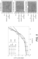
- Atomic force microscope (AFM) images in Figure 1(a) show large particles distributed on the surface prior to snow cleaning, while Figure 1(b) shows that the largest particulates in the population had been completely removed by the cleaning process.
- the root-mean-square roughness for the ITO substrates decreased from 1.76 nm to 1.21 nm, but more importantly, the peak-to-valley roughness decreased from 84.2 nm to 32.4 nm.
- the largest of the particulates is most likely to short the devices as they were larger than the total organic layer thickness, and often were thicker than the entire active organic layer region.
- the particle size count statistics in Figure 1(c) show that snow cleaning had removed most median-sized, and all large particles.
- J sD the donor, deposited directly on the ITO surface, whose leakage was most directly affected by particles on the surface, leading to the observed area dependence of J sD .
- J s and n are the symmetric device saturation current and ideality factor, respectively, J ph is the photocurrent density, k B is the Boltzmann constant, T is the temperature, and q is electronic charge. Finally, ⁇ is the polaron-pair dissociation rate relative to its equilibrium value.
- the simulation showed that FF decreased with R p , and was significantly reduced for R p A ⁇ 2 k ⁇ cm 2 .
- We also plotted the J-V characteristics predicted by Eq. (1) for several values of R p A in Figure 4 , where we assumed R S A 50 ⁇ cm 2 .
- There was a pronounced dependence of FF on R p A which is reflected in the data in Figure 4 . For example, when the shunt resistance was 10 3 ⁇ cm 2 , FF was reduced by 25% from its value when R P A ⁇ .
- the structure with a single subelectrode reduced R S A from 152 ⁇ 4 ⁇ cm 2 to 96 ⁇ 1 ⁇ cm 2 , leading to a corresponding increase of J SC from 4.47 mA/cm 2 to 4.76 mA/cm 2 , FF from 0.29 to 0.40, and ⁇ p from 1.21% to 1.78%.
- the standard deviation in fill factor was -4.0% and was responsible for most of the variation in device efficiency.
- the spread in FF was caused by variations in dark current that arise from increased probability of encountering small particles in large-area devices, and variations in R S A (from 41 ⁇ cm 2 to 69 ⁇ cm 2 ) due to variations encountered while probing devices.
- Snow cleaning of ITO-coated glass substrates is effective in the removal of contaminant particles, hence improving the yield of large-area OPV cells.
- large-area devices exhibited a standard deviation of efficiency of ⁇ 4.0% from the average. Further, the decrease of shunt resistance and increase of dark current due to particulates is evident when only conventional solvent substrate cleaning was employed. The existence of large particulates further resulted in the degradation of large-area device efficiency, fill factor, and yield.
- the relationship between FF and dark current was shown to be sensitive to the existence of shunt paths (and hence R p A) caused by large particles.
- subelectrodes can reduce the series resistance, leading to a power efficiency of 2.21 ⁇ 0.05% of SubPc/C 60 device with an area of 6.25 cm 2 ; or approximately 82% that of an analogous device with an area of only 0.00785 cm 2 .
Landscapes
- Engineering & Computer Science (AREA)
- Chemical & Material Sciences (AREA)
- Nanotechnology (AREA)
- Physics & Mathematics (AREA)
- Electromagnetism (AREA)
- Manufacturing & Machinery (AREA)
- Crystallography & Structural Chemistry (AREA)
- Mathematical Physics (AREA)
- Theoretical Computer Science (AREA)
- Materials Engineering (AREA)
- Photovoltaic Devices (AREA)
- Electroluminescent Light Sources (AREA)
- Cleaning Or Drying Semiconductors (AREA)
- Cleaning In General (AREA)
- Cleaning By Liquid Or Steam (AREA)
Description
- This invention was made with Government support under DE-EE0005310 awarded by the Department of Energy and FA9550-10-1-0339 awarded by the Air Force Office of Scientific Research. The government has certain rights in the invention.
- The subject matter of the present disclosure was made by, on behalf of, and/or in connection with one or more of the following parties to a joint university-corporation research agreement: University of Michigan and Global Photonic Energy Corporation. The agreement was in effect on and before the date the subject matter of the present disclosure was prepared, and was made as a result of activities undertaken within the scope of the agreement.
- The present disclosure generally relates to methods of making organic photovoltaic (OPV) devices, such as solar cells, through the use of large areas of organic molecular layers.
- Photosensitive optoelectronic devices convert electromagnetic radiation into electricity. Solar cells are a type of photosensitive optoelectronic device that are specifically used to generate electrical power.
- To produce internally generated electric fields, the usual method is to juxtapose two layers of material with appropriately selected conductive properties, especially with respect to their distribution of molecular quantum energy states. The interface of these two materials is called a photovoltaic junction. In traditional semiconductor theory, materials for forming PV junctions have been denoted as generally being of either n- or p-type. Here n-type denotes that the majority carrier type is the electron. This could be viewed as the material having many electrons in relatively free energy states. The p-type denotes that the majority carrier type is the hole. Such material has many holes in relatively free energy states. The type of the background, i.e., not photo-generated, majority carrier concentration depends primarily on unintentional doping by defects or impurities. The type and concentration of impurities determine the value of the Fermi energy, or level, within the gap between the conduction band minimum and valance band maximum energies. The Fermi energy characterizes the statistical occupation of molecular quantum energy states denoted by the value of energy for which the probability of occupation is equal to 1/2. A Fermi energy near the conduction band minimum energy indicates that electrons are the predominant carrier. A Fermi energy near the valence band maximum energy indicates that holes are the predominant carrier. Accordingly, the Fermi energy is a primary characterizing property of traditional semiconductors and the prototypical PV junction has traditionally been the p-n interface.
- OPV devices are a promising renewable and green energy source because of their potential for low cost solar energy conversion.
- When an organic material suitable for an optical device is irradiated with appropriate light a photon is absorbed by a molecular component of the material and, as a result, an excited state of the molecular component is produced: an electron is promoted from the HOMO (highest occupied molecular orbital) state to the LUMO (lowest unoccupied molecular orbital) state of the molecule, or a hole is promoted from the LUMO to the HOMO. Thus, an exciton, i.e. an electron-hole pair state is generated. This exciton state has a natural life-time before the electron and the hole will recombine. In order to create a photocurrent the components of the electron-hole pair have to be separated. The separation can be achieved by juxtaposing two layers of materials with different conductive properties. The interface between the layers forms a photovoltaic heterojunction and it should have an asymmetric conduction characteristic, i.e., it should be capable of supporting electronic charge transport preferably in one direction.
- New concepts and approaches have been introduced to improve OPV device performance, and state-of-the-art OPV devices achieve power conversion efficiency values that are close to the threshold required for commercial development. Particulates, however, on substrates (for example, ITO-coated glass), can result in electrical shorts between the electrodes that reduce yield, especially in large-area cells. To develop commercially attractive OPV modules, increasing cell area while maintaining high yield and performance is important.
- Li et al., Proc. SPIE., vol. 6722, p. 672241 (2007) describes cleaning of ITO glass with carbon dioxide snow jet spray.
- Li et al., Proc. SPIE, vol. 7282, p. 72822K (2009) describes ITO glass polishing using carbon dioxide snow jet technique for organic light-emitting diodes.
-
WO 2011/152091 A1 describes an electrode foil which serves as both a supporting base and a reflective electrode, and an organic device which uses the electrode foil. The electrode foil comprises a metal foil and a reflective layer that is provided directly on the metal foil. Prior to the formation of the reflective layer on the metal foil particles on an ultra-smooth surface of the metal foil may be removed using a dry-ice blasting method. - The present disclosure is directed to a process for manufacturing a photovoltaic device according to
claim 1. -
Figure 1 depicts representative atomic force micrographs of the surface of indium tin oxide-coated glass substrates (a) before and (b) after CO2 snow cleaning, and (c) the statistics of particle heights on the two differently treated surfaces. -
Figure 2 depicts (a) series resistance (R s A) and fill factor (FF) for SubPc (open squares and dashed line), and DPSQ (solid squares and solid line) based OPV cells employing a C60 acceptor, (b) Short-circuit current (J SC) and power conversion efficiency (η p) for SubPc and DPSQ OPV devices with different areas. The same line symbols are used as in (a). -
Figure 3 depicts dark current density-vs-voltage (J-V) curves for ITO/MoO3(15 nm)/DPSQ(13 nm)/C60(40 nm)/BCP(8 nm)/Al devices with various active areas. -
Figure 4 depicts calculated dark J-V curves assuming RSA=50 Ω·cm2 and variable RP. Inset: calculated relationship between FF and shunt resistance. -
Figure 5 depicts J-V curves in dark and under 1 sun, AM 1.5G illumination for 6.25 cm2 devices showing the effects of the subelectrode. -
Figure 6 depicts current density vs voltage curves under 1 sun, AM 1.5G illumination for three devices manufactured by a process not in accordance with the claimed subject matter: A, B and C represented by a square, circle and triangle in the legend, respectively.- A: (control device): ITO/MoO3(10nm)/SubPc(13nm)/C60(40nm)/BCP(8 nm)/Al
- B: ITO/PEDOT:PSS(50nm)/MoO3(5nm)/SubPc(13nm)/C60(40nm)/BCP(8 nm)/Al
- C: ITO/MoO3(30nm)/SubPc(13nm)/C60(40nm)/BCP(8 nm)/Al
-
Figure 7 depicts current density vs voltage curves under 1 sun, AM 1.5G illumination for devices having a structure of
ITO/MoO3(10nm)/SubPc(13nm)/C60(40nm)/BCP(8 nm)/Al with various active areas and with snow-plus-solvent cleaned substrates. -
Figure 8 depicts current density vs voltage curves under 1 sun, AM 1.5G illumination for devices having a structure of
ITO/MoO3(10nm)/SubPc(13nm)/C60(40nm)/BCP(8 nm)/Al with various active areas and with only snow-cleaned substrates. -
Figure 9 is an illustration of a snow cleaning apparatus, including a CO2 source, a nozzle and a sample holder. - As used herein, the term "layer" refers to a member or component of a photosensitive device whose primary dimension is X-Y, i.e., along its length and width, and is typically perpendicular to the plane of incidence of the illumination. It should be understood that the term "layer" is not necessarily limited to single layers or sheets of materials. A layer can comprise laminates or combinations of several sheets of materials. In addition, it should be understood that the surfaces of certain layers, including the interface(s) of such layers with other material(s) or layers(s), may be imperfect, wherein said surfaces represent an interpenetrating, entangled or convoluted network with other material(s) or layer(s). Similarly, it should also be understood that a layer may be discontinuous, such that the continuity of said layer along the X-Y dimension may be disturbed or otherwise interrupted by other layer(s) or material(s).
- As used herein, the expression "disposed on" permits other materials or layers to exist between a disposed material and the material on which it is disposed. Likewise, the expression "deposited on" permits other materials or layers to exist between a deposited material and the material on which it is deposited. Thus, other materials or layers may exist between a surface of a substrate and a material "disposed on" or "deposited on" the surface of the substrate.
- As used herein, the term "yield" refers to the proportion of devices, made or manufactured by a process, that performs within a given range of specifications.
- As described herein, exposing the surface of a substrate to a stream of at least one compound comprising one or more phases chosen from supercritical, gaseous, solid, and liquid phases permits the manufacture of large area solar devices having thin organic layers, e.g., a total deposited thickness of ~70 nm, without compromising, and even increasing, yield. In some embodiments, the substrate is an ITO-coated substrate.
- In one embodiment, the process of the present disclosure provides a multi-layer solar device comprising a substrate, and an active area comprising at least one donor material and at least one acceptor material deposited on a surface of the substrate, wherein the donor and acceptor materials are comprised of organic molecules, and wherein particulates are removed from the surface of the substrate before deposition of the donor and acceptor materials. In another embodiment, the process of the present disclosure provides a multi-layer solar device comprising a pre-cleaned substrate having a surface substantially free of particulates, and an active layer comprising at least one donor material and at least one acceptor material disposed on the surface of the substrate, wherein the donor and acceptor materials are comprised of organic molecules.
- The surface of the substrate comprises an electrode, such as an anode or cathode.
- In another embodiment, the process of the present disclosure provides a multi-layer solar device comprising a pre-cleaned substrate having a surface substantially free of particulates, two electrodes in superposed relation disposed on the surface of the pre-cleaned substrate, and an active area comprising at least one donor material and at least one acceptor material, wherein the donor and acceptor materials are comprised of organic molecules located between the two electrodes.
- The particulates are removed by exposing the surface of the substrate to a stream of at least one compound comprising one or more phases chosen from supercritical, gaseous, solid, and liquid phases. This process is referred to herein as "snow cleaning." A substrate is pre-cleaned by snow cleaning.
- In some embodiments, the stream of the at least one compound contains at least gaseous and solid phases. In certain embodiments, the stream of the at least one compound contains gaseous, solid, and liquid phases. In certain embodiments, the stream of the at least one compound comprises a supercritical fluid.
- In some embodiments, the exposure to the stream of the at least one compound is via directed flow. The at least one compound used to remove particulates comprises CO2. This process of CO2 based cleaning is referred to as CO2 snow cleaning, or CO2 cleaning. CO2 snow cleaning is nondestructive, nonabrasive, residue-free, and environmentally friendly.
- In some embodiments, a compound in addition to, CO2 is selected and used in a manner as described herein. The molecule chosen could be selected based on solvation properties for a particular contaminate, or chosen to create a stream containing one or more phases chosen from gas, liquid, solid and supercritical phases. Examples of compounds may include ammonia, nitrous oxide, various hydrocarbons such as acetylene, propane, butane or other hydrocarbons, various chlorinated hydrocarbons such as chloroethanes, various fluorinated hydrocarbons such as fluoroethanes, or mixtures thereof. Exemplary compounds include those that form a liquid or solid upon cooling below room temperature.
- In some embodiments, snow-cleaned substrates are prepared by exposing a surface of the substrate to CO2 around its triple point, i.e., in various parts of the stream, gas, liquid, and solid phases are present.
- In general, snow cleaning relies on the expansion of a liquid or gaseous compound, e.g., CO2, as it emerges from an orifice. The resulting stream of material, e.g, a combination of at least solid and gaseous phases, physically remove particulates by the momentum of the impacting solid particles and/or by the momentum of the gas, thereby overcoming the adhesional force binding particulates to the surface. Other residues on the substrate can be removed by dissolution of contaminates into a liquid or supercritical fluid.
- In some embodiments of the present disclosure, the active area of the solar device ranges from about 0.5 cm2 to 50 cm2, from about 1 cm2 to about 10 cm2, and from about 2.56 cm2 to about 6.25 cm2. In yet another embodiment, the active area ranges from about 0.1 cm2 to about 6.25 cm2.
- In some embodiments, the active area of the solar device is a large area of at least about 0.25 cm2, about 0.5 cm2, about 1 cm2, about 5 cm2, about 6.25 cm2, about 10 cm2, or 50 cm2.
- Removed particulates may vary in size. In some embodiments, particulates that are removed range in diameter from about 5 nm to about 1000 nm, from about 15 nm to about 200 nm, from about 20 nm to about 100 nm, and from about 30 nm to about 60 nm.
- The organic active layer has a thickness ranging from 50 nm to 80 nm.
- The surface of the substrate is cleaned using a technique in addition to snow cleaning, wherein the additional cleaning technique is solvent cleaning. Non-limiting examples of such additional techniques include soaking in solvents such as, for example, trichloroethylene, acetone, and isopropanol.
- In yet another embodiment, snow cleaning increases yield without compromising efficiency. In some embodiments, snow cleaning reduces or eliminates short circuits in the solar device.
- The present disclosure is directed to a process for manufacturing a photovoltaic device comprising, providing a substrate, cleaning a surface of the substrate by exposing the surface to a stream of at least one compound comprising one or more phases chosen from supercritical, gaseous, solid, and liquid phases, and depositing an organic active layer on the surface of the substrate.
- The surface of the substrate exposed to the stream of the at least one compound comprises an electrode, such as an anode or cathode.
- In another embodiment of the present disclosure, a process for manufacturing a photovoltaic device comprises, providing a first electrode layer, cleaning the first electrode layer by exposing the first electrode layer to a stream of at least one compound comprising one or more phases chosen from supercritical, gaseous, solid, and liquid phases, providing a second electrode, wherein an organic active layer is deposited between the first electrode layer and the second electrode layer.
- In yet another embodiment, the present disclosure provides a process for manufacturing a photovoltaic device comprising, providing a first electrode layer, cleaning the first electrode layer by exposing the first electrode layer to a stream of at least one compound comprising one or more phases chosen from supercritical, gaseous, solid, and liquid and combinations thereof, providing a second electrode layer, depositing an organic active layer between the first electrode layer and the second electrode layer, wherein the thickness of the organic active layer is such that it improves yield over a yield obtained without cleaning the first electrode layer with the stream of the at least one compound.
- The organic active layer as used herein may comprise at least one donor material and at least one acceptor material.
- In some embodiments, the stream of the at least one compound contains at least gaseous and solid phases. In certain embodiments, the stream of the at least one compound contains gaseous, solid, and liquid phases. In certain embodiments, the stream of the at least one compound comprises a supercritical fluid.
- In some embodiments, the exposure to the at least one compound is via directed flow. The at least one compound comprises CO2.
- In some embodiments, a compound in addition to CO2 is selected and used in a manner as described herein. The molecule chosen could be selected based on solvation properties for a particular contaminate, or chosen to create a stream containing one or more phases chosen from gas, liquid, solid and supercritical phases. Examples of compounds may include ammonia, nitrous oxide, various hydrocarbons such as acetylene, propane, butane or other hydrocarbons, various chlorinated hydrocarbons such as chloroethanes, various fluorinated hydrocarbons such as fluoroethanes, or mixtures thereof. Exemplary compounds include those that form a liquid or solid upon cooling below room temperature.
- The organic active layer has an area ranging from 0.5 cm2 to 50 cm2, from about 1 cm2 to about 10 cm2, and from about 2.56 cm2 to about 6.25 cm2.
- In some embodiments, the organic active layer has a large area of at least 0.5 cm2, about 1 cm2, about 5 cm2, about 6.25 cm2, or about 10 cm2.
- The organic active layer has a thickness ranging from 50 to 80 nm.
- Additional layers, e.g., buffer layers and smoothing layers, may be deposited between the two electrodes. In some embodiments, the thickness of the deposited layers (e.g., buffer layers, smoothing layers, and/or active layers) are chosen to improve yield. In some embodiments, increasing the thickness of the deposited layers (e.g. buffer layers, smoothing layers, and/or active layers) improves yield.
- In one embodiment, snow cleaning is performed before loading into a chamber, such as in the room ambient. In another embodiment, snow cleaning is performed in a load lock of a deposition tool, wherein the load lock is a chamber that holds a substrate. In some embodiments, the chamber is pumped down, a valve is opened to the chamber, and a substrate is transferred into the chamber. This allows samples to be loaded into the deposition chamber without exposing the chamber to ambient or atmospheric pressure gases.
- In yet another embodiment, snow cleaning is performed in a deposition chamber.
- In one embodiment, the present disclosure relates to an active area within a solar device comprising one or more materials that include a variety of conjugated organic molecules, such as, but not limited to phthalocyanines, functionalized squaraines, functionalized polyacenes, oligothiophenes, merocyanine dyes, modified perylenes (e.g. DIP or DBP) , conducting polymers, low-bandgap polymers, etc. as donor materials, and acceptor materials such as, but not limited to, the fullerenes, C60 or C70, or modified polyacenes such as NTCDA, PTCDA, PTCBI, PTCDI, etc.
- In some embodiments, the organic active layers are deposited on a substrate, for example, a piece of glass, metal or polymer. For solar cells, for example, the substrate may be transparent, such as glass. The substrate comprises an electrode. In particular, the surface of the substrate exposed to the stream of the at least one compound comprises the electrode. The electrode may be applied to serve as a conducting contact to the organic active layers. In some embodiments, the conducting electrode layer comprises an oxide, such as, indium/tin oxide (ITO).
- In another embodiment, OPV devices are made by sandwiching organic layers between two metallic conductors, typically a layer of ITO with high work function and a layer of low work function metal such as Al, Mg or Ag.
- The substrate surface is cleaned and particulates are removed before depositing layers on the substrate.
- In another embodiment, increasing the thickness of deposited layers can at least partially mitigate yield loss. Thickness can be increased by using a buffer layer, e.g., poly (3,4-ethylenedioxythiophene):poly (styrenesulfonate) (PEDOT:PSS) or a thick, e.g., 250 nm, polymer bulk heterojunction active layer or a thicker than normal (t=103 nm) organic layer, e.g., pentacene/C60/BCP. In yet another embodiment, a thick, MoO3 layer can be deposited on a substrate surface, such as an ITO surface.
- In some embodiments, solar cells fabricated and cleaned according to the methods of the present disclosure have a reduced occurrence of electrical shorts. Additionally, in some embodiments, a subelectrode structure may be used to reduce device resistance.
- In accordance with the present disclosure, OPV devices are fabricated using one or more substrate cleaning procedures, including solvent cleaning, in addition to snow cleaning. Snow cleaning, in particular CO2 snow cleaning, was found to be more effective than conventional solvent cleaning in reducing the density of defects that lead to shorts and variations in device performance, especially large-area devices.
- The present disclosure will now be described in greater detail by the following non-limiting examples. It is understood that the skilled artisan will envision additional embodiments consistent with the disclosure provided herein.
- Preparing substrates without snow cleaning: SubPc/C60 devices with areas A>0.64 cm2 have low yield due to shorts caused by particulates. To improve yield, a thick buffer layer (PEDOT:PSS or MoOs) prior to active layer deposition was employed. The device structures were ITO/Buffer layer(s)/SubPc(13 nm)/C60(40 nm)/BCP(8 nm)/Al. Materials were deposited on ITO-coated glass substrates, with an ITO thickness of ~ 100 nm and a sheet resistance of 20±5 Q/sq. MoO3, boron subphthalocyanine chloride (SubPc), C60, and bathocuproine (BCP) were sequentially thermally evaporated at rates of 0.05, 0.1, 0.1, and 0.05 nm/s, respectively, followed by a 100 nm thick Al cathode deposited at 0.1 nm/s through a shadow mask. All deposition rates and thicknesses were measured using a quartz crystal monitor and calibrated by variable angle spectroscopic ellipsometry. MoO3 (Acros, 99.999%) and BCP (Lumtec, 99.5%) were used as received, and SubPc (Lumtec, 99%) and C60 (MER, 99.9%) were further purified in a single cycle by thermal gradient sublimation. In one example, PEDOT:PSS (H.G. Stark, Clevios PH 500) was spun-coated, while MoO3 was thermally evaporated in vacuum.
- The fabricated device structures were as follows:
- Device A (control): ITO/MoO3(10nm)/SubPc(13nm)/C60(40nm)/BCP(8 nm)/Al);
- Device B: ITO/PEDOT:PSS(50nm)/MoO3(5nm)/SubPc(13nm)/C60(40nm)/BCP(8 nm)/Al,
- Device C: ITO/MoO3(30nm)/SubPc(13nm)/C60(40nm)/BCP(8 nm)/Al.
- As shown in Table 1 and
Figure 6 , the increase of deposited layer thickness can degrade device performance. For the small area device (0.00785 cm2), the power conversion efficiency of the control structure (Device A: MoO3(10 nm)) was ηp =2.69±0.03%, decreasing to 2.47±0.08% for devices with a PEDOT:PSS smoothing layer (Device B: PEDOT:PSS(50 nm)/MoO3(5 nm)), and 2.32±0.02% for devices with a relatively thick MoO3 layer (Device C: MoO3(30 nm)). The decrease in efficiency for Devices B and C as compared to A arises primarily from a reduced fill factor. It is foreseeable that one would want to both snow clean and use a thicker buffer layer to minimize shorting as much as possible. - Fitting the dark J-V characteristics following the theory of Giebink, as described in C. Giebink, G.P. Wiederrecht, M.R. Wasielewski, and S.R. Forrest, Phys. Rev. B 82, 155305 (2010), we found that the series resistance of Device C was RSA=5.4±0.1 Ω·cm2 whereas RSA=0.77±0.02 Ω·cm2 for Device A. The increase in RsA was due to the increased MoO3 layer thickness, which in turn led to a reduced FF and thus ηp . Moreover, Device B had a larger dark saturation current density and smaller ideality factor that also led to a reduction in FF.
Table 1 The performance of representative SubPc/C60 devices. Device FF ηP (%) RSA (Ω·cm2) n D J sD (mA/cm2) A 0.621±0.01 2.69±0.03 0.77±0.02 6.7±0.6 (2.8±0.1)×10-7 B 0.56±0.01 2.47±0.08 1.2±0.1 4.5±0.1 (1-3±0.1)×10-4 C 0.53±0.01 2.32±0.02 5.4±0.1 8.4±0.3 (1.5±0.1)×10-5 - An alternative to thicker buffer or active layers is to remove particulates and other asperities from the ITO surface using CO2 snow cleaning. Materials were deposited on ITO-coated glass substrates, with an ITO thickness of ~100 nm and a sheet resistance of 20±5 Q/sq. Prior to film deposition, the ITO was cleaned as follows: first the substrate was gently wiped with a dry particle free wipe followed by 5 minute sonication in a tergitol-deionized water solution, 5 minute sonication in acetone, 10 minute soak in boiling trichloroethylene, 10 minute sonication in acetone, and 10 minute immersion in boiling isopropanol. Snow cleaning was then performed for 90 seconds using an Applied Surface Technologies (New Providence, NJ, 07974) high-purity Model K4 snow cleaner. The substrates were held at 50 °C, with a nozzle angle of 45° with respect to the substrate, and a nozzle-to-substrate distance of ~5 cm. The ITO was then exposed to ultraviolet-ozone for 10 minutes before loading into a high vacuum chamber (base pressure <2×10⁻⁷ Torr). Next, MoOs, boron subphthalocyanine chloride (SubPc), C60, and bathocuproine (BCP) were sequentially thermally sublimed at rates of 0.05, 0.1, 0.1, and 0.05 nm/s, respectively, followed by a 100 nm thick Al cathode deposited at 0.1 nm/s through a shadow mask. All deposition rates and thicknesses were measured using a quartz crystal monitor and calibrated by variable angle spectroscopic ellipsometry. MoO3 (Acros, 99.999%) and BCP (Lumtec, 99.5%) were used as received, and SubPc (Lumtec, 99%) and C60 (MER, 99.9%) were further purified in a single cycle by thermal gradient sublimation.
- Current density-vs.-voltage (J-V) characteristics in the dark and under simulated, 1 sun AM 1.5G solar illumination from a filtered Xe lamp were measured in a high-purity N2 filled glovebox. Optical intensities were referenced using an NREL-calibrated Si detector, and photocurrent measurements were corrected for spectral mismatch. Errors quoted correspond to the standard deviation for a device population of three or more.
- Atomic force microscope (AFM) images in
Figure 1(a) show large particles distributed on the surface prior to snow cleaning, whileFigure 1(b) shows that the largest particulates in the population had been completely removed by the cleaning process. The root-mean-square roughness for the ITO substrates decreased from 1.76 nm to 1.21 nm, but more importantly, the peak-to-valley roughness decreased from 84.2 nm to 32.4 nm. The largest of the particulates is most likely to short the devices as they were larger than the total organic layer thickness, and often were thicker than the entire active organic layer region. The particle size count statistics inFigure 1(c) show that snow cleaning had removed most median-sized, and all large particles. - Large-area, snow-cleaned devices with thin organic layers (i.e. t org≈75 nm) were also fabricated. Thermally evaporated and solution-processed devices with structures of ITO/MoO3(10 nm)/SubPc(13 nm)/C60(40 nm)/BCP(8 nm)/Al (Device D) and ITO/MoO3(15 nm)/DPSQ(13 nm)/C60(40 nm)/BCP(8 nm)/Al (Device E), respectively, were prepared with active areas from 0.01 to 6.25 cm2. The partially solution-processed DPSQ/C60 devices were fabricated where the DPSQ was spin coated on the MoO3 surface from 1.6 mg/ml chloroform solution at a rate of 3000 rpm for 30 seconds.
- As the area increases, no significant changes were observed in the open-circuit voltage (V OC), although the FF decreased for both Devices D and E as shown in
Figure 2 . The decrease in FF was due to the increase in series resistance from RSA≈1 Ω·cm2 for device with A=0.01 cm2, to RSA≈180 Ω·cm2 for the device with A=6.25 cm2, resulting in a concomitant decrease in short-circuit current (J SC). FromFigure 2 , it is apparent that the series resistance needed to be RSA<10 Ω·cm2 to maintain the small-area device performance with increasing device size. - In addition to the increase in RSA, larger area devices can also exhibit high dark current. In
Figure 3 , the dark J-V characteristics for DPSQ/C60 cells with different areas were fitted using the analysis of Giebink described in C. Giebink, G.P. Wiederrecht, M.R. Wasielewski, and S.R. Forrest, Phys. Rev. B 82, 155305 (2010). The results showed that the dark current due to leakage originating from the C60 acceptor layer had an area-independent saturation current density of J sA=(5.7±1.7)×10-11 mA/cm2 and a corresponding ideality factor of n A=1.50±0.01. However, the leakage dark current at low bias (e.g. less than 0.4 V) and often associated with the donor, J sD, increased by approximately 3 decades, from (1.0±0.3)×10-7 mA/cm2 to (0.9±0.1)×10-4 mA/cm2 as area increased from 0.01 cm2 to 6.25 cm2, an approximately linear correspondence. The increased dark current indicated an increased leakage across the donor due to shunt paths induced by particulates not removed by snow cleaning. Hence, it was the donor, deposited directly on the ITO surface, whose leakage was most directly affected by particles on the surface, leading to the observed area dependence of J sD. - In addition to an increase in dark current and series resistance, we also found that FF is reduced by shunt paths. This can be understood by including R p A in the excitonic semiconductor ideal diode equation of Giebink, viz:

- For simplicity, we can consider the case of a symmetric diode, with identical transport properties and injection barriers for both electrons and holes. Here, Js and n are the symmetric device saturation current and ideality factor, respectively, Jph is the photocurrent density, kB is the Boltzmann constant, T is the temperature, and q is electronic charge. Finally, ξ is the polaron-pair dissociation rate relative to its equilibrium value.
-
Figure 4 (inset) shows the dependence of FF on R p A, where JSC = Jph = 4.5 mA/cm2, Js = 1×10⁻⁹ mA/cm2, n = 2, ξ = 1 and RS = 0. The simulation showed that FF decreased with R p, and was significantly reduced for R p A ≤ 2 kΩ·cm2. We also plotted the J-V characteristics predicted by Eq. (1) for several values of R p A inFigure 4 , where we assumed RSA=50 Ω·cm2. There was a pronounced dependence of FF on R p A which is reflected in the data inFigure 4 . For example, when the shunt resistance was 103 Ω·cm2, FF was reduced by 25% from its value when RPA→∞. - Another factor that led to deterioration in large-area OPV performance was the increase of series resistance dominated by the lateral resistance in the ITO layer. To reduce the effect of RS on large-area OPV cells, we used a subelectrode structure for devices D and E (
Figure 5 inset). The subelectrode allowed the carriers to travel a shorter distance from their point of generation before being collected at the metal contact. As shown inFigure 5 , under 1 sun, AM 1.5G illumination, the A=6.25 cm2 SubPc/C60 device with no subelectrode showed η p =1.26±0.05% with JSC =3.55±0.04 mA/cm2, FF=0.32±0.01, and R S A=179±4 Ω·cm2. Cells with a single subelectrode had a decreased series resistance of R S A=78±2 Ω·cm2, resulting in JSC =3.91±0.09 mA/cm2, FF=0.46±0.01, and η p=2.02±0.08%, while four subelectrodes further decreased the resistance to R s A=56±3 Ω·cm2, resulting in J SC=3.95±0.05 mA/cm2, FF=0.50±0.01, and η p=2.21±0.05%. This represented nearly a doubling of η p compared to the device lacking a subelectrode. Similarly, for the DPSQ/C60 device, the structure with a single subelectrode reduced R S A from 152±4 Ω·cm2 to 96±1 Ω·cm2, leading to a corresponding increase of J SC from 4.47 mA/cm2 to 4.76 mA/cm2, FF from 0.29 to 0.40, and η p from 1.21% to 1.78%. - Yields were investigated by fabricating a population of 1.44 cm2 devices. The statistics of nineteen 1.44 cm2 out of twenty-seven total devices with snow-plus-solvent cleaned substrates, and sixteen 1.44 cm2 out of twenty-six devices with snow-cleaned-only substrates (without conventional solvent cleaning) were compared in Table 2.
Table 2 Parameters of OPVs with area of 1.44 cm2 with and without solvent cleaning. The standard deviation from the mean is SD. Cleaning Process V OC(V) Jsc (mA/cm2) FF η P (%) Snow-plussolvent Mean 1.09 4.13 0.56 2.52 SD/Mean 0.4% 1.1% 3.8% 4.0% Snow only Mean 1.10 3.83 0.50 2.10 SD/Mean 1.3% 1.3% 2.7% 3.1% - Using only CO2 snow cleaning, comparable yield of both small and large-area devices were obtained (
Figure 8 ). In contrast, using only solvent cleaning, all devices with area >0.64 cm2 were shorted. Using PEDOT:PSS (Device B) and thicker MoO3 (Device C) coatings on the ITO, the yields of 2.56 cm2 devices were 50% and 67%, respectively. However, the thinner devices using snow-cleaned substrates had a higher yield (~70%). This indicates that CO2 snow cleaning is considerably more effective in reducing surface contaminants than using either thick buffer layers or solvent cleaning alone. For both snow-plus-solvent cleaned (Figure 7 ), and snow-cleaned-only substrates, the standard deviations of V OC and J SC from their mean values were ~1%. The standard deviation in fill factor was -4.0% and was responsible for most of the variation in device efficiency. The spread in FF was caused by variations in dark current that arise from increased probability of encountering small particles in large-area devices, and variations in R S A (from 41 Ω·cm2 to 69 Ω·cm2) due to variations encountered while probing devices. - Snow cleaning of ITO-coated glass substrates is effective in the removal of contaminant particles, hence improving the yield of large-area OPV cells. Using snow cleaning, large-area devices exhibited a standard deviation of efficiency of ≤4.0% from the average. Further, the decrease of shunt resistance and increase of dark current due to particulates is evident when only conventional solvent substrate cleaning was employed. The existence of large particulates further resulted in the degradation of large-area device efficiency, fill factor, and yield. The relationship between FF and dark current was shown to be sensitive to the existence of shunt paths (and hence RpA) caused by large particles. Furthermore, subelectrodes can reduce the series resistance, leading to a power efficiency of 2.21±0.05% of SubPc/C60 device with an area of 6.25 cm2; or approximately 82% that of an analogous device with an area of only 0.00785 cm2.
Claims (6)
- A process for manufacturing a photovoltaic device comprising:providing an electrode layer;cleaning a surface of the electrode layer by exposing the surface to a stream comprising CO2, one or more phases chosen from supercritical, gaseous, solid, and liquid phases; anddepositing an organic active layer on the surface of the electrode layer after the cleaning of the surface of the electrode layer;characterised in that the organic active layer has an area ranging from 0.5 cm2 to 50 cm2, and wherein the organic active layer has a total thickness ranging from 50 nm to 80 nm; andwherein the process further comprises cleaning the surface of the electrode layer with an additional cleaning technique prior to the deposition of the organic active layer, wherein the additional cleaning technique is solvent cleaning.
- The process of claim 1, wherein the stream comprising CO2 contains at least gaseous and solid phases.
- The process of claim 1, wherein the stream comprising CO2 contains gaseous, solid, and liquid phases.
- The process of claim 1, wherein the stream comprising CO2 comprises a supercritical fluid.
- The process of claim 1, wherein the CO2 is chosen to be gaseous at room temperature and atmospheric pressure, optionally wherein the CO2 forms a liquid or solid upon cooling below room temperature.
- The process of claim 1, wherein the CO2 is chosen from a solvent that dissolves a known contaminate.
Applications Claiming Priority (2)
| Application Number | Priority Date | Filing Date | Title |
|---|---|---|---|
| US201261664058P | 2012-06-25 | 2012-06-25 | |
| PCT/US2013/047287 WO2014004364A1 (en) | 2012-06-25 | 2013-06-24 | Large area organic photovoltaics |
Publications (2)
| Publication Number | Publication Date |
|---|---|
| EP2865028A1 EP2865028A1 (en) | 2015-04-29 |
| EP2865028B1 true EP2865028B1 (en) | 2024-04-24 |
Family
ID=48833048
Family Applications (1)
| Application Number | Title | Priority Date | Filing Date |
|---|---|---|---|
| EP13739878.0A Active EP2865028B1 (en) | 2012-06-25 | 2013-06-24 | Large area organic photovoltaics |
Country Status (10)
| Country | Link |
|---|---|
| US (1) | US20150325792A1 (en) |
| EP (1) | EP2865028B1 (en) |
| JP (4) | JP6745598B2 (en) |
| KR (1) | KR102254362B1 (en) |
| CN (1) | CN104603967A (en) |
| AU (1) | AU2013280721A1 (en) |
| CA (1) | CA2877904A1 (en) |
| IL (1) | IL236373A0 (en) |
| TW (1) | TWI599063B (en) |
| WO (1) | WO2014004364A1 (en) |
Families Citing this family (2)
| Publication number | Priority date | Publication date | Assignee | Title |
|---|---|---|---|---|
| US20210028382A1 (en) * | 2019-07-01 | 2021-01-28 | The Regents Of The University Of Michigan | Inverted, semitransparent small molecule photovoltaic cells |
| CN116209331A (en) * | 2021-11-30 | 2023-06-02 | Tcl科技集团股份有限公司 | Photoelectric device processing method and photoelectric device |
Citations (1)
| Publication number | Priority date | Publication date | Assignee | Title |
|---|---|---|---|---|
| WO2011152091A1 (en) * | 2010-06-04 | 2011-12-08 | 三井金属鉱業株式会社 | Electrode foil and organic device |
Family Cites Families (23)
| Publication number | Priority date | Publication date | Assignee | Title |
|---|---|---|---|---|
| JPH05217673A (en) * | 1992-01-31 | 1993-08-27 | Nec Kansai Ltd | Manufacture of thin film el element |
| JPH0679744U (en) * | 1993-04-15 | 1994-11-08 | カシオ計算機株式会社 | Load lock device |
| JP3692380B2 (en) * | 1998-07-03 | 2005-09-07 | Azエレクトロニックマテリアルズ株式会社 | Container cleaning method and apparatus |
| US6726777B1 (en) * | 1999-06-24 | 2004-04-27 | Sumitomo Heavy Industries Ltd. | Cleaning method and apparatus using fluid spraying |
| JP2003209088A (en) * | 2002-01-10 | 2003-07-25 | Sumitomo Heavy Ind Ltd | Aerosol cleaning method and device thereof |
| US6843855B2 (en) * | 2002-03-12 | 2005-01-18 | Applied Materials, Inc. | Methods for drying wafer |
| KR100459717B1 (en) * | 2002-08-23 | 2004-12-03 | 삼성전자주식회사 | Method for forming metal contact in semiconductor device |
| US20070111519A1 (en) * | 2003-10-15 | 2007-05-17 | Applied Materials, Inc. | Integrated electroless deposition system |
| US7375370B2 (en) * | 2004-08-05 | 2008-05-20 | The Trustees Of Princeton University | Stacked organic photosensitive devices |
| US7326955B2 (en) * | 2004-08-05 | 2008-02-05 | The Trustees Of Princeton University | Stacked organic photosensitive devices |
| JP4610308B2 (en) * | 2004-11-16 | 2011-01-12 | 東京エレクトロン株式会社 | Substrate cleaning method, substrate cleaning apparatus, substrate processing system, substrate cleaning program, and storage medium |
| KR100698472B1 (en) * | 2005-07-21 | 2007-03-22 | 주식회사 진우엔지니어링 | Nozzle structure for surface cleaning |
| KR100707881B1 (en) * | 2005-09-23 | 2007-04-13 | 삼성전자주식회사 | System and method for transferring substrates and method for aligning substrates |
| FR2892563B1 (en) * | 2005-10-25 | 2008-06-27 | Commissariat Energie Atomique | POLYMERIC NANOFIBRIDE NETWORK FOR PHOTOVOLTAIC CELLS |
| KR20070047440A (en) * | 2005-11-02 | 2007-05-07 | 삼성전자주식회사 | Manufacturing System and Method of Manufacturing Flat Panel Display |
| CA2737477A1 (en) * | 2008-09-26 | 2010-04-01 | The Regents Of The University Of Michigan | Organic tandem solar cells |
| JP5363164B2 (en) * | 2009-03-31 | 2013-12-11 | 出光興産株式会社 | Benzofluoranthene compound and organic thin film solar cell using the same |
| JP5609008B2 (en) * | 2009-05-12 | 2014-10-22 | コニカミノルタ株式会社 | Transparent conductive film, method for producing transparent conductive film, and transparent electrode for electronic device |
| WO2011074441A1 (en) * | 2009-12-14 | 2011-06-23 | コニカミノルタホールディングス株式会社 | Organic photoelectric conversion element |
| JP5780776B2 (en) * | 2010-03-02 | 2015-09-16 | 国立大学法人九州大学 | Organic thin film solar cell |
| JPWO2011152092A1 (en) * | 2010-06-04 | 2013-07-25 | 三井金属鉱業株式会社 | Electrode foil and organic device |
| JP2012033606A (en) * | 2010-07-29 | 2012-02-16 | Idemitsu Kosan Co Ltd | Photoelectric conversion element |
| JP2012119525A (en) * | 2010-12-01 | 2012-06-21 | Fujifilm Corp | Solar cell element |
-
2013
- 2013-06-24 US US14/410,670 patent/US20150325792A1/en active Pending
- 2013-06-24 AU AU2013280721A patent/AU2013280721A1/en not_active Abandoned
- 2013-06-24 CN CN201380039813.5A patent/CN104603967A/en active Pending
- 2013-06-24 JP JP2015520360A patent/JP6745598B2/en not_active Expired - Fee Related
- 2013-06-24 CA CA2877904A patent/CA2877904A1/en not_active Abandoned
- 2013-06-24 WO PCT/US2013/047287 patent/WO2014004364A1/en not_active Ceased
- 2013-06-24 EP EP13739878.0A patent/EP2865028B1/en active Active
- 2013-06-24 KR KR1020157000395A patent/KR102254362B1/en not_active Expired - Fee Related
- 2013-06-25 TW TW102122565A patent/TWI599063B/en active
-
2014
- 2014-12-21 IL IL236373A patent/IL236373A0/en unknown
-
2018
- 2018-05-23 JP JP2018098977A patent/JP2018152590A/en active Pending
-
2020
- 2020-07-03 JP JP2020115349A patent/JP2020188263A/en active Pending
-
2022
- 2022-07-29 JP JP2022122159A patent/JP2022172080A/en active Pending
Patent Citations (2)
| Publication number | Priority date | Publication date | Assignee | Title |
|---|---|---|---|---|
| WO2011152091A1 (en) * | 2010-06-04 | 2011-12-08 | 三井金属鉱業株式会社 | Electrode foil and organic device |
| EP2579686A1 (en) * | 2010-06-04 | 2013-04-10 | Mitsui Mining & Smelting Co., Ltd | Electrode foil and organic device |
Also Published As
| Publication number | Publication date |
|---|---|
| KR102254362B1 (en) | 2021-05-24 |
| TWI599063B (en) | 2017-09-11 |
| CA2877904A1 (en) | 2014-01-03 |
| JP2020188263A (en) | 2020-11-19 |
| JP2015521806A (en) | 2015-07-30 |
| US20150325792A1 (en) | 2015-11-12 |
| AU2013280721A1 (en) | 2015-01-29 |
| JP2022172080A (en) | 2022-11-15 |
| WO2014004364A1 (en) | 2014-01-03 |
| CN104603967A (en) | 2015-05-06 |
| EP2865028A1 (en) | 2015-04-29 |
| IL236373A0 (en) | 2015-02-26 |
| JP2018152590A (en) | 2018-09-27 |
| TW201403842A (en) | 2014-01-16 |
| KR20150028289A (en) | 2015-03-13 |
| JP6745598B2 (en) | 2020-08-26 |
Similar Documents
| Publication | Publication Date | Title |
|---|---|---|
| Beek et al. | Hybrid zinc oxide conjugated polymer bulk heterojunction solar cells | |
| ES2897925T3 (en) | Organic photosensitive devices with exciton-blocking charge-carrying filters | |
| CN104393176B (en) | It is inverted organic photosensitive devices | |
| JP2016532300A (en) | Exciton blocking treatment of buffer layer in organic photovoltaic technology | |
| KR20120083294A (en) | Bulk heterojunction organic photovoltaic cells made by glancing angle deposition | |
| KR101131564B1 (en) | The effective organic solar cell using core/shell metal oxide nanoparticles and the method for preparing it | |
| EP3726579A1 (en) | Organic photosensitive devices with exciton-blocking charge carrier filters | |
| JP2015501226A (en) | Method for preparing metal substrate surface for organic photosensitive devices | |
| JP2022172080A (en) | Large area organic solar cell | |
| US20130206218A1 (en) | Photovoltaic Devices with Enhanced Exciton Diffusion | |
| Ali et al. | Interface Modification enables 11.95%‐Efficient All‐PbS‐QDs Tandem Solar Cells Utilizing Self‐Assembled Monolayers | |
| Woodhouse et al. | Non-conjugated polymers for organic photovoltaics: Physical and optoelectronic properties of poly (perylene diimides) | |
| Itoh et al. | Enhancement of the open-circuit voltage and hole conduction of tetraphenyl porphyrin/C60 multilayered photovoltaic device by the insertion of oxide hole collection layers | |
| Hancox | Utilising high work function metal oxides as hole extracting layers for organic photovoltaic cells | |
| Forrest et al. | Inverted organic photosensitive devices | |
| Ng | Design and optimization of thin film organic solar cells | |
| Choi | Topics in quantum transport of charge and heat in solid state systems | |
| Bernède et al. | About the transparent electrode of the organic photovoltaic cells | |
| Qasem | On Absorption-Enhanced Organic Photovoltaic By Incorporating Metallic Nano Pyramid Particles | |
| Hughes | Organic thin-film photovoltaic cells: an investigation of fabrication methods. | |
| Steensma | Improving the performance of nickel oxide-based MAPbI3 perovskite solar cells | |
| Ho et al. | Efficiency Improvement of Organic Solar Cell with Metal Anode by Using Wet Oxidation |
Legal Events
| Date | Code | Title | Description |
|---|---|---|---|
| PUAI | Public reference made under article 153(3) epc to a published international application that has entered the european phase |
Free format text: ORIGINAL CODE: 0009012 |
|
| 17P | Request for examination filed |
Effective date: 20150116 |
|
| AK | Designated contracting states |
Kind code of ref document: A1 Designated state(s): AL AT BE BG CH CY CZ DE DK EE ES FI FR GB GR HR HU IE IS IT LI LT LU LV MC MK MT NL NO PL PT RO RS SE SI SK SM TR |
|
| AX | Request for extension of the european patent |
Extension state: BA ME |
|
| RIN1 | Information on inventor provided before grant (corrected) |
Inventor name: FORREST, STEPHEN, R. Inventor name: ZIMMERMAN, JERAMY Inventor name: WANG, NANA |
|
| DAX | Request for extension of the european patent (deleted) | ||
| STAA | Information on the status of an ep patent application or granted ep patent |
Free format text: STATUS: EXAMINATION IS IN PROGRESS |
|
| 17Q | First examination report despatched |
Effective date: 20200210 |
|
| P01 | Opt-out of the competence of the unified patent court (upc) registered |
Effective date: 20230511 |
|
| REG | Reference to a national code |
Ref country code: DE Ref legal event code: R079 Free format text: PREVIOUS MAIN CLASS: H01L0051000000 Ipc: H10K0071000000 Ref country code: DE Ref legal event code: R079 Ref document number: 602013085623 Country of ref document: DE Free format text: PREVIOUS MAIN CLASS: H01L0051000000 Ipc: H10K0071000000 |
|
| GRAP | Despatch of communication of intention to grant a patent |
Free format text: ORIGINAL CODE: EPIDOSNIGR1 |
|
| STAA | Information on the status of an ep patent application or granted ep patent |
Free format text: STATUS: GRANT OF PATENT IS INTENDED |
|
| RIC1 | Information provided on ipc code assigned before grant |
Ipc: H10K 77/10 20230101ALI20230811BHEP Ipc: H10K 30/81 20230101ALI20230811BHEP Ipc: H10K 71/00 20230101AFI20230811BHEP |
|
| INTG | Intention to grant announced |
Effective date: 20230905 |
|
| GRAJ | Information related to disapproval of communication of intention to grant by the applicant or resumption of examination proceedings by the epo deleted |
Free format text: ORIGINAL CODE: EPIDOSDIGR1 |
|
| STAA | Information on the status of an ep patent application or granted ep patent |
Free format text: STATUS: EXAMINATION IS IN PROGRESS |
|
| GRAP | Despatch of communication of intention to grant a patent |
Free format text: ORIGINAL CODE: EPIDOSNIGR1 |
|
| STAA | Information on the status of an ep patent application or granted ep patent |
Free format text: STATUS: GRANT OF PATENT IS INTENDED |
|
| INTC | Intention to grant announced (deleted) | ||
| INTG | Intention to grant announced |
Effective date: 20240108 |
|
| GRAS | Grant fee paid |
Free format text: ORIGINAL CODE: EPIDOSNIGR3 |
|
| GRAA | (expected) grant |
Free format text: ORIGINAL CODE: 0009210 |
|
| STAA | Information on the status of an ep patent application or granted ep patent |
Free format text: STATUS: THE PATENT HAS BEEN GRANTED |
|
| AK | Designated contracting states |
Kind code of ref document: B1 Designated state(s): AL AT BE BG CH CY CZ DE DK EE ES FI FR GB GR HR HU IE IS IT LI LT LU LV MC MK MT NL NO PL PT RO RS SE SI SK SM TR |
|
| REG | Reference to a national code |
Ref country code: GB Ref legal event code: FG4D |
|
| REG | Reference to a national code |
Ref country code: CH Ref legal event code: EP |
|
| REG | Reference to a national code |
Ref country code: DE Ref legal event code: R096 Ref document number: 602013085623 Country of ref document: DE |
|
| REG | Reference to a national code |
Ref country code: IE Ref legal event code: FG4D |
|
| REG | Reference to a national code |
Ref country code: LT Ref legal event code: MG9D |
|
| REG | Reference to a national code |
Ref country code: NL Ref legal event code: MP Effective date: 20240424 |
|
| REG | Reference to a national code |
Ref country code: AT Ref legal event code: MK05 Ref document number: 1681020 Country of ref document: AT Kind code of ref document: T Effective date: 20240424 |
|
| PG25 | Lapsed in a contracting state [announced via postgrant information from national office to epo] |
Ref country code: NL Free format text: LAPSE BECAUSE OF FAILURE TO SUBMIT A TRANSLATION OF THE DESCRIPTION OR TO PAY THE FEE WITHIN THE PRESCRIBED TIME-LIMIT Effective date: 20240424 |
|
| PG25 | Lapsed in a contracting state [announced via postgrant information from national office to epo] |
Ref country code: NL Free format text: LAPSE BECAUSE OF FAILURE TO SUBMIT A TRANSLATION OF THE DESCRIPTION OR TO PAY THE FEE WITHIN THE PRESCRIBED TIME-LIMIT Effective date: 20240424 |
|
| PG25 | Lapsed in a contracting state [announced via postgrant information from national office to epo] |
Ref country code: IS Free format text: LAPSE BECAUSE OF FAILURE TO SUBMIT A TRANSLATION OF THE DESCRIPTION OR TO PAY THE FEE WITHIN THE PRESCRIBED TIME-LIMIT Effective date: 20240824 |
|
| PG25 | Lapsed in a contracting state [announced via postgrant information from national office to epo] |
Ref country code: BG Free format text: LAPSE BECAUSE OF FAILURE TO SUBMIT A TRANSLATION OF THE DESCRIPTION OR TO PAY THE FEE WITHIN THE PRESCRIBED TIME-LIMIT Effective date: 20240424 |
|
| PG25 | Lapsed in a contracting state [announced via postgrant information from national office to epo] |
Ref country code: HR Free format text: LAPSE BECAUSE OF FAILURE TO SUBMIT A TRANSLATION OF THE DESCRIPTION OR TO PAY THE FEE WITHIN THE PRESCRIBED TIME-LIMIT Effective date: 20240424 Ref country code: FI Free format text: LAPSE BECAUSE OF FAILURE TO SUBMIT A TRANSLATION OF THE DESCRIPTION OR TO PAY THE FEE WITHIN THE PRESCRIBED TIME-LIMIT Effective date: 20240424 |
|
| PG25 | Lapsed in a contracting state [announced via postgrant information from national office to epo] |
Ref country code: GR Free format text: LAPSE BECAUSE OF FAILURE TO SUBMIT A TRANSLATION OF THE DESCRIPTION OR TO PAY THE FEE WITHIN THE PRESCRIBED TIME-LIMIT Effective date: 20240725 |
|
| PG25 | Lapsed in a contracting state [announced via postgrant information from national office to epo] |
Ref country code: PT Free format text: LAPSE BECAUSE OF FAILURE TO SUBMIT A TRANSLATION OF THE DESCRIPTION OR TO PAY THE FEE WITHIN THE PRESCRIBED TIME-LIMIT Effective date: 20240826 |
|
| PG25 | Lapsed in a contracting state [announced via postgrant information from national office to epo] |
Ref country code: ES Free format text: LAPSE BECAUSE OF FAILURE TO SUBMIT A TRANSLATION OF THE DESCRIPTION OR TO PAY THE FEE WITHIN THE PRESCRIBED TIME-LIMIT Effective date: 20240424 |
|
| PG25 | Lapsed in a contracting state [announced via postgrant information from national office to epo] |
Ref country code: AT Free format text: LAPSE BECAUSE OF FAILURE TO SUBMIT A TRANSLATION OF THE DESCRIPTION OR TO PAY THE FEE WITHIN THE PRESCRIBED TIME-LIMIT Effective date: 20240424 |
|
| PG25 | Lapsed in a contracting state [announced via postgrant information from national office to epo] |
Ref country code: PL Free format text: LAPSE BECAUSE OF FAILURE TO SUBMIT A TRANSLATION OF THE DESCRIPTION OR TO PAY THE FEE WITHIN THE PRESCRIBED TIME-LIMIT Effective date: 20240424 |
|
| PG25 | Lapsed in a contracting state [announced via postgrant information from national office to epo] |
Ref country code: LV Free format text: LAPSE BECAUSE OF FAILURE TO SUBMIT A TRANSLATION OF THE DESCRIPTION OR TO PAY THE FEE WITHIN THE PRESCRIBED TIME-LIMIT Effective date: 20240424 |
|
| PG25 | Lapsed in a contracting state [announced via postgrant information from national office to epo] |
Ref country code: PT Free format text: LAPSE BECAUSE OF FAILURE TO SUBMIT A TRANSLATION OF THE DESCRIPTION OR TO PAY THE FEE WITHIN THE PRESCRIBED TIME-LIMIT Effective date: 20240826 Ref country code: PL Free format text: LAPSE BECAUSE OF FAILURE TO SUBMIT A TRANSLATION OF THE DESCRIPTION OR TO PAY THE FEE WITHIN THE PRESCRIBED TIME-LIMIT Effective date: 20240424 Ref country code: NO Free format text: LAPSE BECAUSE OF FAILURE TO SUBMIT A TRANSLATION OF THE DESCRIPTION OR TO PAY THE FEE WITHIN THE PRESCRIBED TIME-LIMIT Effective date: 20240724 Ref country code: LV Free format text: LAPSE BECAUSE OF FAILURE TO SUBMIT A TRANSLATION OF THE DESCRIPTION OR TO PAY THE FEE WITHIN THE PRESCRIBED TIME-LIMIT Effective date: 20240424 Ref country code: IS Free format text: LAPSE BECAUSE OF FAILURE TO SUBMIT A TRANSLATION OF THE DESCRIPTION OR TO PAY THE FEE WITHIN THE PRESCRIBED TIME-LIMIT Effective date: 20240824 Ref country code: HR Free format text: LAPSE BECAUSE OF FAILURE TO SUBMIT A TRANSLATION OF THE DESCRIPTION OR TO PAY THE FEE WITHIN THE PRESCRIBED TIME-LIMIT Effective date: 20240424 Ref country code: GR Free format text: LAPSE BECAUSE OF FAILURE TO SUBMIT A TRANSLATION OF THE DESCRIPTION OR TO PAY THE FEE WITHIN THE PRESCRIBED TIME-LIMIT Effective date: 20240725 Ref country code: FI Free format text: LAPSE BECAUSE OF FAILURE TO SUBMIT A TRANSLATION OF THE DESCRIPTION OR TO PAY THE FEE WITHIN THE PRESCRIBED TIME-LIMIT Effective date: 20240424 Ref country code: ES Free format text: LAPSE BECAUSE OF FAILURE TO SUBMIT A TRANSLATION OF THE DESCRIPTION OR TO PAY THE FEE WITHIN THE PRESCRIBED TIME-LIMIT Effective date: 20240424 Ref country code: BG Free format text: LAPSE BECAUSE OF FAILURE TO SUBMIT A TRANSLATION OF THE DESCRIPTION OR TO PAY THE FEE WITHIN THE PRESCRIBED TIME-LIMIT Effective date: 20240424 Ref country code: AT Free format text: LAPSE BECAUSE OF FAILURE TO SUBMIT A TRANSLATION OF THE DESCRIPTION OR TO PAY THE FEE WITHIN THE PRESCRIBED TIME-LIMIT Effective date: 20240424 Ref country code: RS Free format text: LAPSE BECAUSE OF FAILURE TO SUBMIT A TRANSLATION OF THE DESCRIPTION OR TO PAY THE FEE WITHIN THE PRESCRIBED TIME-LIMIT Effective date: 20240724 |
|
| PG25 | Lapsed in a contracting state [announced via postgrant information from national office to epo] |
Ref country code: DK Free format text: LAPSE BECAUSE OF FAILURE TO SUBMIT A TRANSLATION OF THE DESCRIPTION OR TO PAY THE FEE WITHIN THE PRESCRIBED TIME-LIMIT Effective date: 20240424 |
|
| PG25 | Lapsed in a contracting state [announced via postgrant information from national office to epo] |
Ref country code: EE Free format text: LAPSE BECAUSE OF FAILURE TO SUBMIT A TRANSLATION OF THE DESCRIPTION OR TO PAY THE FEE WITHIN THE PRESCRIBED TIME-LIMIT Effective date: 20240424 |
|
| PG25 | Lapsed in a contracting state [announced via postgrant information from national office to epo] |
Ref country code: CZ Free format text: LAPSE BECAUSE OF FAILURE TO SUBMIT A TRANSLATION OF THE DESCRIPTION OR TO PAY THE FEE WITHIN THE PRESCRIBED TIME-LIMIT Effective date: 20240424 |
|
| PG25 | Lapsed in a contracting state [announced via postgrant information from national office to epo] |
Ref country code: RO Free format text: LAPSE BECAUSE OF FAILURE TO SUBMIT A TRANSLATION OF THE DESCRIPTION OR TO PAY THE FEE WITHIN THE PRESCRIBED TIME-LIMIT Effective date: 20240424 Ref country code: SK Free format text: LAPSE BECAUSE OF FAILURE TO SUBMIT A TRANSLATION OF THE DESCRIPTION OR TO PAY THE FEE WITHIN THE PRESCRIBED TIME-LIMIT Effective date: 20240424 |
|
| REG | Reference to a national code |
Ref country code: DE Ref legal event code: R097 Ref document number: 602013085623 Country of ref document: DE |
|
| PG25 | Lapsed in a contracting state [announced via postgrant information from national office to epo] |
Ref country code: SM Free format text: LAPSE BECAUSE OF FAILURE TO SUBMIT A TRANSLATION OF THE DESCRIPTION OR TO PAY THE FEE WITHIN THE PRESCRIBED TIME-LIMIT Effective date: 20240424 |
|
| PG25 | Lapsed in a contracting state [announced via postgrant information from national office to epo] |
Ref country code: SM Free format text: LAPSE BECAUSE OF FAILURE TO SUBMIT A TRANSLATION OF THE DESCRIPTION OR TO PAY THE FEE WITHIN THE PRESCRIBED TIME-LIMIT Effective date: 20240424 Ref country code: SK Free format text: LAPSE BECAUSE OF FAILURE TO SUBMIT A TRANSLATION OF THE DESCRIPTION OR TO PAY THE FEE WITHIN THE PRESCRIBED TIME-LIMIT Effective date: 20240424 Ref country code: RO Free format text: LAPSE BECAUSE OF FAILURE TO SUBMIT A TRANSLATION OF THE DESCRIPTION OR TO PAY THE FEE WITHIN THE PRESCRIBED TIME-LIMIT Effective date: 20240424 Ref country code: EE Free format text: LAPSE BECAUSE OF FAILURE TO SUBMIT A TRANSLATION OF THE DESCRIPTION OR TO PAY THE FEE WITHIN THE PRESCRIBED TIME-LIMIT Effective date: 20240424 Ref country code: DK Free format text: LAPSE BECAUSE OF FAILURE TO SUBMIT A TRANSLATION OF THE DESCRIPTION OR TO PAY THE FEE WITHIN THE PRESCRIBED TIME-LIMIT Effective date: 20240424 Ref country code: CZ Free format text: LAPSE BECAUSE OF FAILURE TO SUBMIT A TRANSLATION OF THE DESCRIPTION OR TO PAY THE FEE WITHIN THE PRESCRIBED TIME-LIMIT Effective date: 20240424 Ref country code: MC Free format text: LAPSE BECAUSE OF FAILURE TO SUBMIT A TRANSLATION OF THE DESCRIPTION OR TO PAY THE FEE WITHIN THE PRESCRIBED TIME-LIMIT Effective date: 20240424 |
|
| REG | Reference to a national code |
Ref country code: CH Ref legal event code: PL |
|
| PG25 | Lapsed in a contracting state [announced via postgrant information from national office to epo] |
Ref country code: LU Free format text: LAPSE BECAUSE OF NON-PAYMENT OF DUE FEES Effective date: 20240624 |
|
| PLBE | No opposition filed within time limit |
Free format text: ORIGINAL CODE: 0009261 |
|
| STAA | Information on the status of an ep patent application or granted ep patent |
Free format text: STATUS: NO OPPOSITION FILED WITHIN TIME LIMIT |
|
| GBPC | Gb: european patent ceased through non-payment of renewal fee |
Effective date: 20240724 |
|
| 26N | No opposition filed |
Effective date: 20250127 |
|
| PG25 | Lapsed in a contracting state [announced via postgrant information from national office to epo] |
Ref country code: IE Free format text: LAPSE BECAUSE OF NON-PAYMENT OF DUE FEES Effective date: 20240624 |
|
| PG25 | Lapsed in a contracting state [announced via postgrant information from national office to epo] |
Ref country code: SI Free format text: LAPSE BECAUSE OF FAILURE TO SUBMIT A TRANSLATION OF THE DESCRIPTION OR TO PAY THE FEE WITHIN THE PRESCRIBED TIME-LIMIT Effective date: 20240424 Ref country code: CH Free format text: LAPSE BECAUSE OF NON-PAYMENT OF DUE FEES Effective date: 20240630 Ref country code: BE Free format text: LAPSE BECAUSE OF NON-PAYMENT OF DUE FEES Effective date: 20240630 |
|
| PG25 | Lapsed in a contracting state [announced via postgrant information from national office to epo] |
Ref country code: FR Free format text: LAPSE BECAUSE OF NON-PAYMENT OF DUE FEES Effective date: 20240624 |
|
| PG25 | Lapsed in a contracting state [announced via postgrant information from national office to epo] |
Ref country code: GB Free format text: LAPSE BECAUSE OF NON-PAYMENT OF DUE FEES Effective date: 20240724 |
|
| REG | Reference to a national code |
Ref country code: BE Ref legal event code: MM Effective date: 20240630 |
|
| PGFP | Annual fee paid to national office [announced via postgrant information from national office to epo] |
Ref country code: DE Payment date: 20250618 Year of fee payment: 13 |
|
| PG25 | Lapsed in a contracting state [announced via postgrant information from national office to epo] |
Ref country code: SE Free format text: LAPSE BECAUSE OF FAILURE TO SUBMIT A TRANSLATION OF THE DESCRIPTION OR TO PAY THE FEE WITHIN THE PRESCRIBED TIME-LIMIT Effective date: 20240424 |
|
| PG25 | Lapsed in a contracting state [announced via postgrant information from national office to epo] |
Ref country code: CY Free format text: LAPSE BECAUSE OF FAILURE TO SUBMIT A TRANSLATION OF THE DESCRIPTION OR TO PAY THE FEE WITHIN THE PRESCRIBED TIME-LIMIT; INVALID AB INITIO Effective date: 20130624 |
|
| PG25 | Lapsed in a contracting state [announced via postgrant information from national office to epo] |
Ref country code: IT Free format text: LAPSE BECAUSE OF FAILURE TO SUBMIT A TRANSLATION OF THE DESCRIPTION OR TO PAY THE FEE WITHIN THE PRESCRIBED TIME-LIMIT Effective date: 20240424 |
|
| PG25 | Lapsed in a contracting state [announced via postgrant information from national office to epo] |
Ref country code: HU Free format text: LAPSE BECAUSE OF FAILURE TO SUBMIT A TRANSLATION OF THE DESCRIPTION OR TO PAY THE FEE WITHIN THE PRESCRIBED TIME-LIMIT; INVALID AB INITIO Effective date: 20130624 |