JP4610308B2 - Substrate cleaning method, substrate cleaning apparatus, substrate processing system, substrate cleaning program, and storage medium - Google Patents
Substrate cleaning method, substrate cleaning apparatus, substrate processing system, substrate cleaning program, and storage medium Download PDFInfo
- Publication number
- JP4610308B2 JP4610308B2 JP2004332080A JP2004332080A JP4610308B2 JP 4610308 B2 JP4610308 B2 JP 4610308B2 JP 2004332080 A JP2004332080 A JP 2004332080A JP 2004332080 A JP2004332080 A JP 2004332080A JP 4610308 B2 JP4610308 B2 JP 4610308B2
- Authority
- JP
- Japan
- Prior art keywords
- substrate
- back surface
- vicinity
- wafer
- cleaning
- Prior art date
- Legal status (The legal status is an assumption and is not a legal conclusion. Google has not performed a legal analysis and makes no representation as to the accuracy of the status listed.)
- Expired - Fee Related
Links
Images


Description
本発明は、基板洗浄方法、基板洗浄装置、基板処理システム、基板洗浄プログラム及び記憶媒体に関し、特に、基板の裏面に付着した付着物を除去する基板洗浄方法に関する。 The present invention relates to a substrate cleaning method, a substrate cleaning apparatus, a substrate processing system, a substrate cleaning program, and a storage medium, and more particularly to a substrate cleaning method for removing deposits attached to the back surface of a substrate.
通常、基板としての半導体ウエハ(以下「ウエハ」という。)に任意の処理を施す基板処理装置では、ウエハと該ウエハを載置する載置台との接触に起因するパーティクル、例えばアルミの金属片や、処理ガスの反応に起因する反応生成物、例えば、フルオロカーボン系のポリマー等が発生する。これらのパーティクルは、ウエハに付着して該ウエハの表面に形成された半導体デバイスの品質を低下させる。 Usually, in a substrate processing apparatus that performs arbitrary processing on a semiconductor wafer (hereinafter referred to as “wafer”) as a substrate, particles caused by contact between the wafer and a mounting table on which the wafer is mounted, for example, a metal piece of aluminum, Then, a reaction product resulting from the reaction of the processing gas, such as a fluorocarbon polymer, is generated. These particles adhere to the wafer and degrade the quality of the semiconductor device formed on the surface of the wafer.
ウエハに付着したパーティクルを除去する方法として、ドライエッチング処理が施されたウエハをウェット処理室においてフッ酸溶液や純水によって水洗するウエット洗浄方法が知られている。該方法によれば、ドライエッチング処理中にウエハに付着したパーティクルを除去することができる(例えば、特許文献1参照。)。
しかしながら、上述したウエット洗浄方法では、主にウエハの表面に向けて純水等を吹き付けるため、ウエハの裏面に付着したパーティクル、具体的にはウエハの裏面の全面に亘って付着したパーティクルやウエハの裏面の周縁部に付着したベベルポリマー(Bevel Polymer)を除去することができない。 However, in the above-described wet cleaning method, pure water or the like is mainly sprayed toward the front surface of the wafer. Therefore, particles adhering to the back surface of the wafer, specifically, particles adhering to the entire back surface of the wafer, The bevel polymer attached to the peripheral edge of the back surface cannot be removed.
ウエハの裏面に付着したパーティクルは、ウエハを載置台に載置した際、該ウエハを浮き上がらせるため、ウエハの表面に塗布されたフォトレジストを露光するリソグラフィー工程において、ウエハと露光装置との距離が露光装置の焦点距離に一致せず、ウエハの表面に正確なマスクパターンを再現できず、該ウエハから製造される半導体デバイスの品質を低下させるという問題がある。 Particles adhering to the back surface of the wafer lift the wafer when the wafer is placed on the mounting table. Therefore, in the lithography process for exposing the photoresist applied to the wafer surface, the distance between the wafer and the exposure apparatus is There is a problem that it does not match the focal length of the exposure apparatus, an accurate mask pattern cannot be reproduced on the surface of the wafer, and the quality of a semiconductor device manufactured from the wafer is deteriorated.
また、所定のプラズマ処理が施されたウエハは、複数枚のウエハを互いに平行に保持する密閉容器、例えば、フープ(Foup)等に収容されて搬送されるが、該フープ内において上方に位置するウエハの裏面からパーティクルが剥離して下方に位置するウエハの表面に落下して付着し、該下方のウエハから製造される半導体デバイスの品質を低下させるという問題がある。 The wafer subjected to the predetermined plasma treatment is transported while being accommodated in a hermetic container that holds a plurality of wafers in parallel with each other, for example, a FOUP, etc., and is positioned above the FOUP. There is a problem in that particles are peeled off from the back surface of the wafer and dropped and adhered to the surface of the wafer located below to deteriorate the quality of a semiconductor device manufactured from the wafer below.
さらに、上述したウエット洗浄方法において、仮にウエハの裏面のパーティクルやベベルポリマーが除去されたとしても、ウエット洗浄における純水の流れは制御されていないため、除去されたパーティクル等がウエット洗浄されているウエハの隣で、所定の処理、例えば、乾燥処理が施されているウエハの表面に再付着して、やはり、該ウエハから製造される半導体デバイスの品質を低下させるという問題がある。 Further, in the above-described wet cleaning method, even if particles and bevel polymer on the back surface of the wafer are removed, the flow of pure water in the wet cleaning is not controlled, so the removed particles are wet cleaned. Next to the wafer, there is a problem that it adheres again to the surface of the wafer which has been subjected to a predetermined process, for example, a drying process, and the quality of the semiconductor device manufactured from the wafer is deteriorated.
本発明の目的は、基板の裏面に付着した付着物を完全に除去すると共に、基板から製造される半導体デバイスの品質の低下を防止することができる基板洗浄方法、基板洗浄装置、基板処理システム、基板洗浄プログラム及び記憶媒体を提供することにある。 SUMMARY OF THE INVENTION An object of the present invention is to provide a substrate cleaning method, a substrate cleaning apparatus, a substrate processing system, which can completely remove deposits attached to the back surface of a substrate and prevent deterioration of the quality of a semiconductor device manufactured from the substrate. A substrate cleaning program and a storage medium are provided.
上記目的を達成するために、請求項1記載の基板洗浄方法は、所定の処理が施される基板の裏面を洗浄する基板洗浄方法であって、前記基板の裏面に2つの相状態を呈する物質を接触させて、前記基板の裏面に付着した付着物を剥離させる2相状態物質接触ステップと、所定の圧力下において前記基板の裏面の近傍に前記物質による粘性流の流れを生成させて、前記基板の裏面から剥離した付着物を前記基板の裏面近傍から排除する裏面近傍流生成ステップと、前記基板の裏面近傍から排除された付着物を排出する排出ステップとを有することを特徴とする。
In order to achieve the above object, the substrate cleaning method according to
請求項2記載の基板洗浄方法は、請求項1記載の基板洗浄方法において、前記2つの相状態を呈する物質はエアロゾルを含む所定の気体であることを特徴とする。
The substrate cleaning method according to
請求項3記載の基板洗浄方法は、請求項1又は2記載の基板洗浄方法において、前記所定の圧力は133Pa(1Torr)以上であることを特徴とする。
The substrate cleaning method according to
請求項4記載の基板洗浄方法は、請求項1記載の基板洗浄方法において、前記2つの相状態を呈する物質は超臨界状態の物質であることを特徴とする。 According to a fourth aspect of the present invention, there is provided the substrate cleaning method according to the first aspect, wherein the substance exhibiting the two phase states is a supercritical substance.
請求項5記載の基板洗浄方法は、請求項4記載の基板洗浄方法において、前記超臨界状態の物質は、前記基板に付着する付着物を溶解する所定の添加剤を含むことを特徴とする。 A substrate cleaning method according to a fifth aspect is the substrate cleaning method according to the fourth aspect, wherein the supercritical substance includes a predetermined additive that dissolves deposits adhering to the substrate.
請求項6記載の基板洗浄方法は、請求項5記載の基板洗浄方法において、前記2相状態物質接触ステップは、前記所定の添加剤を含まない前記超臨界状態の物質を前記基板の表面に接触させ、且つ前記所定の添加剤を含む前記超臨界状態の物質を前記基板の裏面に接触させることを特徴とする。
6. The substrate cleaning method according to
上記目的を達成するために、請求項7記載の基板洗浄方法は、所定の処理が施される基板の裏面を洗浄する基板洗浄方法であって、前記基板の裏面に高エネルギーの光を照射して、前記基板の裏面に付着した付着物を剥離させる高エネルギー光照射ステップと、所定の圧力下において前記基板の裏面の近傍に物質による粘性流の流れを生成させて、前記基板の裏面から剥離した付着物を前記基板の裏面近傍から排除する裏面近傍流生成ステップと、前記基板の裏面近傍から排除された付着物を排出する排出ステップとを有することを特徴とする。
To achieve the above object, a substrate cleaning method according to
請求項8記載の基板洗浄方法は、請求項7記載の基板洗浄方法において、前記物質は2つの相状態を呈する物質であることを特徴とする。
The substrate cleaning method according to
請求項9記載の基板洗浄方法は、請求項8記載の基板洗浄方法において、前記2つの相状態を呈する物質はエアロゾルを含む所定の気体であることを特徴とする。
The substrate cleaning method according to
請求項10記載の基板洗浄方法は、請求項8記載の基板洗浄方法において、前記2つの相状態を呈する物質は超臨界状態の物質であることを特徴とする。
The substrate cleaning method according to
上記目的を達成するために、請求項11記載の基板洗浄装置は、所定の処理が施される基板の裏面を洗浄する基板洗浄装置であって、前記基板の裏面に2つの相状態を呈する物質を接触させて、前記基板の裏面に付着した付着物を剥離させる2相状態物質接触手段と、所定の圧力下において前記基板の裏面の近傍に前記物質による粘性流の流れを生成させ、前記基板の裏面から剥離した付着物を前記基板の裏面近傍から排除する裏面近傍流生成手段と、前記基板の裏面近傍から排除された付着物を排出する排出手段と、を備えることを特徴とする。 To achieve the above object, the substrate cleaning apparatus according to claim 11 exhibiting, a substrate cleaning apparatus for cleaning the back surface of the substrate which is subjected to predetermined processing, the two-phase state on the back surface of the substrate material are contacted, and the two-phase state material contacting means deposits Ru is peeled adhered to the back surface of the substrate, to generate a flow of viscous flow due to the material in the vicinity of the back surface of the substrate under a predetermined pressure, the and back near flow generating means you eliminate deposits peeled from the back surface of the substrate from the back surface near the substrate, characterized in that and a discharge means for discharging the deposits which have been excluded from the back surface near the substrate .
上記目的を達成するために、請求項12記載の基板洗浄装置は、所定の処理が施される基板の裏面を洗浄する基板洗浄装置であって、前記基板の裏面に高エネルギーの光を照射して、前記基板の裏面に付着した付着物を剥離させる高エネルギー光照射手段と、所定の圧力下において前記基板の裏面の近傍に前記物質による粘性流の流れを生成させて、前記基板の裏面から剥離した付着物を前記基板の裏面近傍から排除する裏面近傍流生成手段と、前記基板の裏面近傍から排除された付着物を排出する排出手段とを備えることを特徴とする。
To achieve the above object, the substrate cleaning apparatus according to
上記目的を達成するために、請求項13記載の基板処理システムは、基板に所定の処理を施す少なくとも1つの基板処理装置と、前記基板の裏面を洗浄する基板洗浄装置とを備える基板処理システムであって、前記基板洗浄装置は、前記基板の裏面に2つの相状態を呈する物質を接触させて、前記基板の裏面に付着した付着物を剥離させる2相状態物質接触手段と、所定の圧力下において前記基板の裏面の近傍に前記物質による粘性流の流れを生成させて、前記基板の裏面から剥離した付着物を前記基板の裏面近傍から排除する裏面近傍流生成手段と、前記基板の裏面近傍から排除された付着物を排出する排出手段とを有することを特徴とする。
In order to achieve the above object, a substrate processing system of
上記目的を達成するために、請求項14記載の基板処理システムは、基板に所定の処理を施す少なくとも1つの基板処理装置と、前記基板の裏面を洗浄する基板洗浄装置とを備える基板処理システムであって、前記基板洗浄装置は、前記基板の裏面に高エネルギーの光を照射して、前記基板の裏面に付着した付着物を剥離させる高エネルギー光照射手段と、所定の圧力下において前記基板の裏面の近傍に前記物質による粘性流の流れを生成させて、前記基板の裏面から剥離した付着物を前記基板の裏面近傍から排除する裏面近傍流生成手段と、前記基板の裏面近傍から排除された付着物を排出する排出手段とを有することを特徴とする。
In order to achieve the above object, a substrate processing system of
上記目的を達成するために、請求項15記載の基板洗浄プログラムは、所定の処理が施される基板の裏面を洗浄する基板洗浄方法をコンピュータに実行させる基板洗浄プログラムであって、前記基板洗浄方法が、前記基板の裏面に2つの相状態を呈する物質を接触させて前記基板の裏面に付着した付着物を剥離させる2相状態物質接触ステップと、所定の圧力下において前記基板の裏面の近傍に前記物質による粘性流の流れを生成させて、前記基板の裏面から剥離した付着物を前記基板の裏面近傍から排除する裏面近傍流生成ステップと、前記基板の裏面近傍から排除された付着物を排出する排出ステップとを有することを特徴とする。
In order to achieve the above object, a substrate cleaning program according to
上記目的を達成するために、請求項16記載の基板洗浄プログラムは、所定の処理が施される基板の裏面を洗浄する基板洗浄方法をコンピュータに実行させる基板洗浄プログラムであって、前記基板洗浄方法が、前記基板の裏面に高エネルギーの光を照射して、前記基板の裏面に付着した付着物を剥離させる高エネルギー光照射ステップと、所定の圧力下において前記基板の裏面の近傍に前記物質による粘性流の流れを生成させて、前記基板の裏面から剥離した付着物を前記基板の裏面近傍から排除する裏面近傍流生成ステップと、前記基板の裏面近傍から排除された付着物を排出する排出ステップとを有することを特徴とする。
In order to achieve the above object, a substrate cleaning program according to
上記目的を達成するために、請求項17記載の記憶媒体は、所定の処理が施される基板の裏面を洗浄する基板洗浄方法を実行させるプログラムを格納するコンピュータが読み取り可能な記憶媒体であって、前記基板洗浄方法が、前記基板の裏面に2つの相状態を呈する物質を接触させて前記基板の裏面に付着した付着物を剥離させる2相状態物質接触ステップと、所定の圧力下において前記基板の裏面の近傍に前記物質による粘性流の流れを生成させて、前記基板の裏面から剥離した付着物を前記基板の裏面近傍から排除する裏面近傍流生成ステップと、前記基板の裏面近傍から排除された付着物を排出する排出ステップとを有することを特徴とする。
To achieve the above object, a storage medium according to
上記目的を達成するために、請求項18記載の記憶媒体は、所定の処理が施される基板の裏面を洗浄する基板洗浄方法を実行させるプログラムを格納するコンピュータが読み取り可能な記憶媒体であって、前記基板洗浄方法が、前記基板の裏面に高エネルギーの光を照射して、前記基板の裏面に付着した付着物を剥離させる高エネルギー光照射ステップと、所定の圧力下において前記基板の裏面の近傍に前記物質による粘性流の流れを生成させて、前記基板の裏面から剥離した付着物を前記基板の裏面近傍から排除する裏面近傍流生成ステップと、前記基板の裏面近傍から排除された付着物を排出する排出ステップとを有することを特徴とする。
In order to achieve the above object, a storage medium according to
請求項1記載の基板洗浄方法、請求項11記載の基板洗浄装置、請求項13記載の基板処理システム、請求項15記載の基板洗浄プログラム及び請求項17記載の記憶媒体によれば、基板の裏面に2つの相状態を呈する物質が接触し、所定の圧力下において基板の裏面の近傍に該物質の流れが生成される。2つの相状態を呈する物質は、各相状態が有する特性を備えるので、各特性の相乗効果によって基板の裏面に付着した付着物を効率よく除去することができる。また、所定の圧力下において生成された物質の流れは粘性流を形成するので、基板の裏面から除去した付着物を基板の裏面近傍から効率よく排除する。これにより、基板の裏面に付着した付着物を完全に除去することができると共に、基板から製造される半導体デバイスの品質の低下を防止することができる。
According to the substrate cleaning method of
請求項2及び9記載の基板洗浄方法によれば、2つの相状態を呈する物質はエアロゾルを含む所定の気体である。エアロゾルは基板の裏面に付着した付着物に衝突して該付着物の付着力を低下させて除去し、気体は除去された付着物を運搬する。これにより、基板の裏面に付着した付着物を確実に除去することができる。 According to the substrate cleaning method of the second and ninth aspects, the substance exhibiting two phase states is a predetermined gas containing aerosol. The aerosol collides with the deposits attached to the back surface of the substrate and lowers the adhesion force of the deposits to remove them, and the gas carries the removed deposits. Thereby, the deposit | attachment adhering to the back surface of a board | substrate can be removed reliably.
請求項3記載の基板洗浄方法によれば、所定の圧力は133Pa(1Torr)以上であるので、物質の流れを確実に粘性流とすることができ、もって基板の裏面から除去された付着物を基板の裏面近傍から確実に排除することができる。 According to the substrate cleaning method of the third aspect, since the predetermined pressure is 133 Pa (1 Torr) or more, the flow of the substance can be surely made a viscous flow, and the deposits removed from the back surface of the substrate can be removed. It can be reliably excluded from the vicinity of the back surface of the substrate.
請求項4及び10記載の基板洗浄方法によれば、2つの相状態を呈する物質は超臨界状態の物質である。超臨界状態の物質は気相状態及び液相状態の特性を有するので、気相状態の特性によって基板の裏面及び付着物の境界面近傍まで回り込んで付着物の付着力を低下させ、液相状態の特性によって付着力の低下した付着物を巻き込む。これにより、基板の裏面に付着した付着物を確実に除去することができる。
According to the substrate cleaning method of
請求項5記載の基板洗浄方法によれば、超臨界状態の物質は基板に付着する付着物を溶解する所定の添加剤を含む。該添加剤は超臨界状態の物質の特性によって付着物の周囲を隙間無く包囲する。これにより、付着物を効率よく溶解することができる。 According to the substrate cleaning method of the fifth aspect, the supercritical substance includes a predetermined additive that dissolves deposits adhering to the substrate. The additive surrounds the deposit without gaps depending on the properties of the supercritical material. Thereby, a deposit can be dissolved efficiently.
請求項6記載の基板洗浄方法によれば、所定の添加剤を含まない超臨界状態の物質が基板の表面に接触し、且つ所定の添加剤を含む超臨界状態の物質が基板の裏面に接触する。したがって、溶解した付着物を含む基板の裏面近傍における超臨界状態の物質が基板の表面に回り込むことがないため、溶解した付着物が基板の表面に再度付着するのを確実に防止することができる。
According to the substrate cleaning method of
請求項7記載の基板洗浄方法、請求項12記載の基板洗浄装置、請求項14記載の基板処理システム、請求項16記載の基板洗浄プログラム及び請求項18記載の記憶媒体によれば、基板の裏面に高エネルギーの光が照射され、所定の圧力下において基板の裏面の近傍に物質の流れが生成される。高エネルギーの光が照射された基板は膨張して基板の裏面及び付着物との間に膨張量差を発生させることによって基板の裏面に付着した付着物を効率よく除去する。また、所定の圧力下において生成された物質の流れは粘性流を形成するので、基板の裏面から除去された付着物を基板の裏面近傍から効率よく排除する。これにより、基板の裏面に付着した付着物を完全に除去することができ、もって基板から製造される半導体デバイスの品質の低下を防止することができる。
According to a substrate cleaning method according to
請求項8記載の基板洗浄方法によれば、物質は2つの相状態を呈するので、各相状態が有する特性の相乗効果によって基板の裏面に付着した付着物をより効率よく除去することができる。 According to the substrate cleaning method of the eighth aspect, since the substance exhibits two phase states, it is possible to more efficiently remove deposits attached to the back surface of the substrate due to the synergistic effect of the characteristics of each phase state.
以下、本発明の実施の形態について図面を参照しながら説明する。 Hereinafter, embodiments of the present invention will be described with reference to the drawings.
まず、本発明の第1の実施の形態に係る基板洗浄装置及び基板処理システムについて説明する。 First, a substrate cleaning apparatus and a substrate processing system according to a first embodiment of the present invention will be described.
図1は、本実施の形態に係る基板処理システムの概略構成を示す平面図である。 FIG. 1 is a plan view showing a schematic configuration of a substrate processing system according to the present embodiment.
図1において、クラスタ型の基板処理システム1は、多角形状を呈する搬送室2と、該搬送室2の周囲に配され且つ搬送室2の側壁にゲートバルブ3a〜3eを介して接続されるプラズマ処理室としての真空室4a〜4eと、該真空室4と同様に搬送室2の側壁にゲートバルブ3fを介して接続される1つのクリーニング室(基板洗浄装置)5と、搬送室2の側壁に直接接続される2つのカセット室6a,bとを備える。
In FIG. 1, a cluster type
搬送室2は旋回自在且つ伸縮自在であるスカラ型の搬送アーム7を有し、該搬送アーム7は基板処理システム1において半導体ウエハWを所望の位置へ搬送することが可能である。各真空室4は半導体ウエハWを載置する載置台8を有し、該載置台8に載置された半導体ウエハWに所定のプラズマ処理、例えば、エッチング処理を施す。
The
クリーニング室5は半導体ウエハWを保持するグリップアーム22を有し、該グリップアーム22に保持された半導体ウエハWの裏面(以下「ウエハ裏面」という。)を洗浄する。各カセット室6は複数の未処理又は処理済みの半導体ウエハWを収容するカセット(図示しない)を有する。各ゲートバルブ3は開閉自在なスライド扉であり、各真空室4及び搬送室2、又はクリーニング室5及び搬送室2を連通・遮断する。
The
基板処理システム1では、半導体ウエハWにプラズマ処理が施される場合、搬送アーム7がカセット室6aのカセットから未処理の半導体ウエハWを搬出し且つ該半導体ウエハWを真空室4へ搬入する。該真空室4は搬入された半導体ウエハWにプラズマ処理を施し、搬送アーム7は該プラズマ処理が施された半導体ウエハWをクリーニング室5に搬入する。該クリーニング室5は搬入されたウエハ裏面を後述するウエハ裏面洗浄方法で洗浄し、搬送アーム7は裏面が洗浄された半導体ウエハWをカセット室6bのカセットへ搬入する。
In the
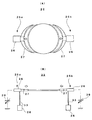
図2は、図1における線II−IIに沿う断面図である。 2 is a cross-sectional view taken along line II-II in FIG.
図2において、クリーニング室5は、気密に構成された円筒状の主チャンバ9と、該主チャンバ9の上部に設けられたガス導入部10と、主チャンバ9の下部に設けられたガス排出部11とを備える。
In FIG. 2, the
ガス導入部10は、主チャンバ9の上面に穿孔された数多くのガス導入孔12と、該ガス導入孔12の上方に設けられたバッファ室13と、主チャンバ9から離間して配置されるガス供給部14と、バッファ室13及びガス供給部14を接続するガス導入管15と、該ガス導入管15の途中に設けられたバルブ16とからなる。このガス導入部10は、ウエハ裏面を洗浄する際、バルブ16を開弁し、ガス供給部14からN2ガス等をガス導入管15、バッファ室13及びガス導入孔12を介して主チャンバ9内へ供給し、該主チャンバ9内において下降流を発生させる。
The
ガス排出部11は、主チャンバ9の下面に開口するガス吸入孔17と、該ガス吸入孔17の下方に設けられたバッファ室18と、主チャンバ9から離間して配置される排気ポンプ19と、バッファ室18及び排気ポンプ19を接続するガス排出管20と、該ガス排出管20の途中に設けられたバルブ21とからなる。このガス排出部11は、ウエハ裏面を洗浄する際、バルブ21を開弁し、排気ポンプ19を作動させて、主チャンバ9内のガスをガス吸入孔17、バッファ室18及びガス排出管20を介して排出する。また、このとき、ガス排出部11は主チャンバ9のガスを下方に向けて吸引するので、該主チャンバ9内において発生したガス導入部10による下降流が助長される。
The
主チャンバ9は、グリップアーム22と、該グリップアーム22に保持された半導体ウエハWの下方に配置されるエアロゾル噴射部23と、保持された半導体ウエハWの上方に配置される2つの加熱ランプ24とを有する。
The
図3は、図2におけるグリップアームの概略構成を示す図であり、図3(A)はグリップアームの平面図であり、図3(B)はグリップアームの側面図である。 3 is a diagram showing a schematic configuration of the grip arm in FIG. 2, FIG. 3 (A) is a plan view of the grip arm, and FIG. 3 (B) is a side view of the grip arm.
図3において、グリップアーム22は、一対のウエハ側面保持部25a,bを有する。各ウエハ側面保持部25は、アーム基部26と、該アーム基部26から突出自在なアーム部27と、アーム基部26に振動伝達棒33を介して接続される超音波振動部28と、アーム基部26に接続される直流電源29とからなる。アーム部27は上面視三日月形状を呈する板状部材であり、半導体ウエハWに対向する部位(以下「ウエハ対向部位」という。)の曲率は、半導体ウエハWの外周における曲率と一致する。
In FIG. 3, the
主チャンバ9内に搬送アーム7によってプラズマ処理済みの半導体ウエハWが搬入された場合、グリップアーム22は、各ウエハ側面保持部25のアーム部27を図中矢印方向に沿ってアーム基部26から突出させ、アーム部27のウエハ対向部位を半導体ウエハWの外周部に当接させることにより、半導体ウエハWを保持する。このとき、半導体ウエハWは外周部のみがアーム部27と当接するので、半導体ウエハWの表面及び裏面は露出する。
When the semiconductor wafer W that has been subjected to plasma processing is carried into the
また、超音波振動部28が超音波振動を発振し、該超音波振動はアーム基部26及びアーム部27を介して半導体ウエハWに伝達され、直流電源29はアーム基部26及びアーム部27を介して半導体ウエハWに電圧を印加する。
The
各加熱ランプ24は、グリップアーム22に保持された半導体ウエハWの上面に熱線を照射することによって半導体ウエハWの温度を上昇させる。
Each
図4は、図2におけるエアロゾル噴射部の概略構成を示す図であり、図4(A)はエアロゾル噴射部の側面図であり、図4(B)はエアロゾル噴射部におけるラバルノズルの断面図である。 4 is a diagram showing a schematic configuration of the aerosol injection unit in FIG. 2, FIG. 4 (A) is a side view of the aerosol injection unit, and FIG. 4 (B) is a sectional view of a Laval nozzle in the aerosol injection unit. .
図4において、エアロゾル噴射部23は、グリップアーム22に保持された半導体ウエハWと平行に配置されるガイドレール30と、該ガイドレール30に沿って移動するノズル基部31と、該ノズル基部31の上方に設けられ、所定の仰角でウエハ裏面を指向するラバル(先細末広)ノズル32とを有する。
In FIG. 4, the
ラバルノズル32は、金属、例えば、アルミから成る円管状部材であり、管内の空間がガス流路として機能する。また、ラバルノズル32では、ガスが流入する上流側端部(図4(B)における左側の端部)33aから下流側端部(図4(B)における右側の端部)33bに架けて内径が変化する。具体的には、内径が上流側端部33aから下流側端部33bに向けてまず縮小し、上流側端部33aから所定の距離の点より下流側では拡大する。すなわち、ラバルノズル32のガス流路は途中に咽部34を有する。なお、本実施の形態では、以下、上流側端部33aから咽部34までを縮小部と称し、咽部34から下流側端部33bまでを拡大部と称する。
The
ラバルノズル32は、上流側端部33a、咽部34及び下流側端部33bにおける内径、並びに縮小部や拡大部の長さ等を適切に設定することにより、上流側端部33aに流入したガス流の流速を音速以上まで高めて下流側端部33bより噴射することが可能である。本実施の形態では、拡大部においてガスの流速が超音速となるようにラバルノズル32の諸寸法が設定されている。
The
また、拡大部において流速の音速突破に伴い発生する衝撃波の波面が停滞し、停止衝撃波が形成される。これにより、ラバルノズル32の前後、具体的には上流側端部33aから下流側端部33bまでの圧力勾配が不連続になる。このとき、下流側端部33b側における圧力、すなわち、主チャンバ9の圧力に対して上流側端部33a側における圧力を高めることによって容易にガスの流速をラバルノズル32内において超音速に到達させることができる。本実施の形態では、主チャンバ9内の圧力が数kPa(数10Torr)に設定され、これに対して上流側端部33a側における圧力は大気圧(100kPa(760Torr))に設定されるのが好ましい。
In addition, the wave front of the shock wave generated with the sonic breakthrough of the flow velocity is stagnated in the enlarged portion, and a stop shock wave is formed. As a result, the pressure gradient before and after the
拡大部においてガスの流速が超音速となると、該ガス流は膨張流れとなり、断熱膨張によって流速の増加に応じて該ガスの温度が低下する。そのため、ラバルノズル32から噴射されたガスの温度は急速に低下し、該ガスの凝固点を下回る。このとき、ガスの流れにおいてガスが凝固した微少な粒子(エアロゾル(Aerosol))が発生する。ラバルノズル32が噴射するガスは固体粒子(エアロゾル)を含むため、2つの相状態を呈する。
When the flow velocity of the gas becomes supersonic in the enlarged portion, the gas flow becomes an expansion flow, and the temperature of the gas decreases as the flow velocity increases due to adiabatic expansion. Therefore, the temperature of the gas injected from the
ウエハ裏面を洗浄する際、ラバルノズル32はエアロゾルを含むガス(以下「エアロゾルガス」という。)を噴射するが、上述したように、ラバルノズル32はウエハ裏面を指向するので、ガスはウエハ裏面に衝突する。このとき、衝突するガスに含まれたエアロゾルがウエハ裏面の全面に亘って付着したパーティクルPや裏面の周縁部に付着したベベルポリマーBPに衝突すると、パーティクルPやベベルポリマーBPに運動エネルギーを付与し、該運動エネルギーを付与されたパーティクルP等はウエハ裏面から剥離する。また、運動エネルギーをパーティクルPに付与したエアロゾルは、半導体ウエハWや該半導体ウエハWの周辺雰囲気から熱エネルギーを付与されて気化する。
When cleaning the back surface of the wafer, the
エアロゾルから気化したガスや、エアロゾルを含んでいたガスはウエハ裏面に衝突して、半導体ウエハWの周縁部へ向かうガス流を生成する。ウエハ裏面から剥離したパーティクルP等は、このガス流によってウエハ裏面からガス排出部11へ向けて運搬され、ガス排出部11によって主チャンバ9から排出される。
The gas vaporized from the aerosol or the gas containing the aerosol collides with the back surface of the wafer and generates a gas flow toward the peripheral edge of the semiconductor wafer W. Particles P and the like separated from the back surface of the wafer are transported from the back surface of the wafer toward the
また、ウエハ裏面を洗浄する際、ノズル基部31はガイドレール30に沿って図4(A)中に示す矢印方向に移動する。ノズル基部31が移動する間、ラバルノズル32はエアロゾルガスをウエハ裏面に向けて噴射するので、エアロゾル噴射部23はエアロゾルガスの流れによってウエハ裏面を全面に亘って走査することができ、これにより、ウエハ裏面の全面からパーティクルP等を除去することができる。
Further, when the wafer back surface is cleaned, the
上述したように、エアロゾル噴射部23は半導体ウエハWの下方に設けられるため、エアロゾルガスは半導体ウエハWの下方からウエハ裏面に衝突する。これにより、ウエハ裏面から剥離したパーティクルP等を重力によって下方、すなわち、ガス排出部11の方へ効率よく運搬することができる。
As described above, since the
また、ガス導入部10からN2ガスが導入される。これにより、主チャンバ9内においてN2ガスの下降流が発生し、剥離したパーティクルP等が主チャンバ9内を上昇して半導体ウエハWの表面(以下「ウエハ表面」という。)側に回り込んでウエハ表面に付着するのを防止できる。
Further, N 2 gas is introduced from the
ウエハ裏面を洗浄する際における主チャンバ9内の圧力は133Pa(1Torr)以上であることが好ましい。主チャンバ9内の圧力が133Pa以上であれば、ウエハ裏面近傍に発生するガスの流れ、例えば、上述したエアロゾルから気化したガスのガス流や上述した下降流が確実に粘性流となり、そのガス粘性力が大きくなるため、ウエハ裏面から剥離したパーティクルP等をウエハ裏面近傍から確実に運搬して除去することができる。
The pressure in the
ラバルノズル32から噴射されるガスは、圧力の急変に応じて爆発することのないガスである必要があり、例えば、He(ヘリウム),Ne(ネオン),Ar(アルゴン),Kr(クリプトン),Xe(キセノン),Rn(ラドン)等の希ガスや、N2,CO2,O2,F2,Cl2,Br2等のいずれかを用いることができる。
The gas injected from the
以上、エアロゾル噴射部23によるウエハ裏面のパーティクルP等の除去について説明したが、パーティクルP等のウエハ裏面からの剥離を促進するために、クリーニング室5では、他の構成要素が以下に説明するように作動する。
The removal of the particles P and the like on the back surface of the wafer by the
まず、超音波振動部28が超音波振動を発振し、該超音波振動をアーム基部26及びアーム部27を介して半導体ウエハWに伝達する。超音波振動を伝達された半導体ウエハWでは、パーティクルP等の半導体ウエハWに対する付着力が低下するため、パーティクルP等の剥離が促進される。
First, the
また、直流電源29はアーム基部26及びアーム部27を介して半導体ウエハWに電圧を印加する。このとき、半導体ウエハWへの電圧の印加に起因して主チャンバ9において電場が発生し、ウエハ裏面に電磁応力(Electromagnetic Stress)が作用する。電磁応力は、互いに隣接する誘電率が異なる物質の周辺で電場が発生したときに、物質同士を離間させるように働く斥力であるため、ウエハ裏面に付着したパーティクルPの付着力が弱まり、パーティクルP等の剥離が促進される。
The
ここで、クリーニング室5では、直流電源29が極性の異なる電圧を交互に半導体ウエハWへ印加するのが好ましい。上記電磁応力は、半導体ウエハWへの電圧の印加及び停止の切替時において裏面に効果的に作用するため、ウエハ裏面に効果的な電磁応力が繰り返して作用する。したがって、ウエハ裏面に付着したパーティクルP等の剥離を十分に促進することができる。また、半導体ウエハWへ極性の異なる電圧が交互に印加されるため、半導体ウエハWが帯電するのを防止することができる。
Here, in the
なお、直流電源29が半導体ウエハWに印加する電圧は、主チャンバ9内の圧力に応じて変化するが、半導体ウエハWにチャージアップダメージが発生しない程度、例えば、数100Vであるのが好ましい。
Note that the voltage applied to the semiconductor wafer W by the
さらに、各加熱ランプ24は、グリップアーム22に保持された半導体ウエハWの上面に熱線を照射することによって半導体ウエハWの温度を上昇させる。このとき、半導体ウエハWと主チャンバ9の壁面との間に温度勾配が形成され、半導体ウエハW(高温部)から該壁面(低温部)に向けて熱泳動力がパーティクルP等に発生する。これにより、ウエハ裏面に付着したパーティクルPの付着力が弱まり、パーティクルP等の剥離が促進される。
Furthermore, each
尚、上述したクリーニング室5の各構成要素の動作は、基板処理システム1が有するパーソナルコンピュータ(図示しない)によって制御される。
The operation of each component of the
次に、本実施の形態に係る基板洗浄方法について説明する。 Next, the substrate cleaning method according to the present embodiment will be described.
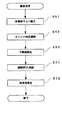
図5は、本実施の形態に係る基板洗浄方法としてのウエハ裏面洗浄処理のフローチャートである。 FIG. 5 is a flowchart of wafer back surface cleaning processing as a substrate cleaning method according to the present embodiment.
図5において、まず、搬送アーム7が真空室4においてプラズマ処理が施された半導体ウエハWをクリーニング室5の主チャンバ9に搬入し(ステップS51)、グリップアーム22が該搬入された半導体ウエハWを保持する。
In FIG. 5, first, the
次いで、ガス排出部11が主チャンバ9内の空気を排出して主チャンバ9内を数kPaに調整し(ステップS52)、ガス導入部10がN2ガスを主チャンバ9内へ供給し、該主チャンバ9内において下降流を発生させる(ステップS53)。
Next, the
次いで、エアロゾル噴射部23において、ノズル基部31がガイドレール30に沿って移動を開始すると共に、ラバルノズル32がエアロゾルガスをウエハ裏面に向けて噴射する(2相状態物質接触ステップ)(ステップS54)。このとき、エアロゾルがウエハ裏面に付着したパーティクルP等に衝突して該パーティクルP等を剥離させる。また、直流電源29が半導体ウエハWに交互に電圧を印加し、超音波振動部28が半導体ウエハWに超音波振動を伝達し、各加熱ランプ24が半導体ウエハWの温度を上昇させてパーティクルP等の剥離を促進する。
Next, in the
次いで、エアロゾルから気化したガスや、エアロゾルを含んでいたガスは、ウエハ裏面と衝突して半導体ウエハWの外縁へ向かうガス流を発生させるが、このとき、主チャンバ9内の圧力が数kPaに調整されているので、該ガス流はガス粘性流となる(裏面近傍流生成ステップ)(ステップS55)。該ガス粘性流はウエハ裏面から剥離したパーティクルP等をウエハ裏面近傍から確実に運搬して除去する。
Next, the gas vaporized from the aerosol or the gas containing the aerosol collides with the back surface of the wafer and generates a gas flow toward the outer edge of the semiconductor wafer W. At this time, the pressure in the
エアロゾル噴射部23は、ノズル基部31が移動する間、ステップS54及びS55を継続して実行することによってウエハ裏面をエアロゾルガスの流れによって走査する。そして、ノズル基部31の移動が終了すると、本処理を終了する。
The
上述した本実施の形態に係る基板洗浄装置、基板処理システム及び基板洗浄方法によれば、ウエハ裏面にエアロゾルガスが接触し、数kPaの主チャンバ9内の圧力下においてウエハ裏面の近傍にエアロゾルから気化したガスやエアロゾルを含んでいたガスのガス流が生成される。エアロゾルガスは、各相(気相、固相)状態が有する特性を備えるので、各特性の相乗効果によってウエハ裏面に付着したパーティクルP等を効率よく除去することができる。具体的には、エアロゾルがウエハ裏面のパーティクルP等に衝突して運動エネルギーを該パーティクルPに付与し、該パーティクルPを剥離させる。さらに、エアロゾルから気化したガスやエアロゾルを含んでいたガスのガス流は剥離したパーティクルP等を運搬する。また、数kPaの圧力下においてガス流は粘性流を形成するので、ウエハ裏面から剥離パーティクルP等をウエハ裏面近傍から効率よく排除する。これにより、ウエハ裏面に付着したパーティクルP等を完全に除去することができると共に、半導体ウエハWから製造される半導体デバイスの品質の低下を防止することができる。
According to the substrate cleaning apparatus, the substrate processing system, and the substrate cleaning method according to the present embodiment described above, the aerosol gas is in contact with the back surface of the wafer, and from the aerosol near the back surface of the wafer under the pressure in the
上述した本実施の形態におけるラバルノズル32では、拡大部において停止衝撃波を発生させたが、上流側端部33a側における圧力及び下流側端部33b側における圧力を調整することによって、停止衝撃波をラバルノズル32の外部において発生させてもよい。
In the above-described
具体的には、上流側端部33a側における圧力を大気圧より高く設定し、且つ下流側端部33b側における圧力を主チャンバ9内の圧力より低く設定する。このとき、ラバルノズル32から噴射されたエアロゾルガスは過膨張となり、停止衝撃波がラバルノズル32の外部において発生する。また、停止衝撃波をウエハ裏面において発生させるのが好ましい。これにより、停止衝撃波の振動が半導体ウエハWに伝達され、該振動によってパーティクルP等の付着力が低下し、該パーティクルP等の剥離が促進される。
Specifically, the pressure on the upstream end 33 a side is set higher than the atmospheric pressure, and the pressure on the downstream end 33 b side is set lower than the pressure in the
尚、上述した本実施の形態では、半導体ウエハWがグリップアーム22によって保持され、エアロゾル噴射部23におけるノズル基部31が移動することによってウエハ裏面をエアロゾルガスで走査したが、ノズル基部31が固定され且つグリップアーム22が半導体ウエハWを移動させることによってウエハ裏面をエアロゾルガスで走査してもよい。
In the above-described embodiment, the semiconductor wafer W is held by the
次に、本発明の第2の実施の形態に係る基板洗浄装置について説明する。 Next, a substrate cleaning apparatus according to the second embodiment of the present invention will be described.
本実施の形態は、その構成、作用が上述した第1の実施の形態と基本的に同じであり、ウエハ裏面を洗浄する際に上述したエアロゾルガスではなく、超臨界状態の物質を用いる点で異なるのみである。したがって、重複した構成、作用については説明を省略し、以下に異なる構成、作用についての説明を行う。 This embodiment is basically the same in configuration and operation as the first embodiment described above, and uses a supercritical substance instead of the aerosol gas described above when cleaning the wafer back surface. Only different. Therefore, the description of the duplicated configuration and operation is omitted, and the description of the different configuration and operation is given below.
図6は、本実施の形態に係る基板処理装置としてのクリーニング室の概略構成を示す断面図である。 FIG. 6 is a cross-sectional view showing a schematic configuration of a cleaning chamber as a substrate processing apparatus according to the present embodiment.
図6において、クリーニング室60は、主チャンバ9と、ガス導入部10と、ガス排出部11とを備え、該主チャンバ9は、グリップアーム22と、該グリップアーム22に保持された半導体ウエハWの表面及び裏面に後述する超臨界状態のCO2を供給する超臨界流体供給部61と、2つの加熱ランプ24と、主チャンバ9内の雰囲気を加熱するヒータ(図示しない)とを有する。
In FIG. 6, the cleaning
超臨界流体供給部61は、グリップアーム22に保持されたウエハ表面上方に向けて超臨界状態のCO2を図中矢印方向に沿って供給する上部処理流体供給源62と、ウエハ裏面下方に向けて超臨界状態のCO2を図中矢印方向に沿って供給する下部処理流体供給源63とを有する。
Supercritical
超臨界状態とは、或る物質の気体若しくは液体が、気体と液体が共存できる限界の温度・圧力(臨界点)を超えて所定の高温・高圧状態に達したときに、気体と液体の密度が同じになって2相(気相・液相)が区別できなくなり、気液の境界面が消失した状態である。該超臨界状態の物質は2相の特性を併せ持つため、超臨界状態の物質からなる流体(以下「超臨界流体」という。)は、気相の特性によってウエハ表面に形成された半導体デバイスの微細な窪みに侵入し、液相の特性によって微細な窪みに存在するパーティクル等を巻き込んで運搬する。超臨界流体を形成する物質としては、H2O(水)、CO2、NH3(アンモニア)、CH4(メタン)、C3H8(プロパン)、CH3OH(メタノール)、又はC2H5OH(エタノール)等があり、例えば、CO2は31.1℃、7.37MPaの条件下で超臨界状態に達する。 The supercritical state is the density of a gas or liquid when the gas or liquid of a certain substance reaches a predetermined high temperature and high pressure state exceeding the limit temperature and pressure (critical point) at which the gas and liquid can coexist. The two phases (gas phase and liquid phase) cannot be distinguished from each other, and the gas-liquid interface has disappeared. Since the material in the supercritical state has two-phase characteristics, a fluid composed of the material in the supercritical state (hereinafter referred to as “supercritical fluid”) is a fine structure of a semiconductor device formed on the wafer surface due to the gas phase characteristics. It penetrates into a hollow and entrains and transports particles and the like present in the fine depression depending on the characteristics of the liquid phase. Substances that form a supercritical fluid include H 2 O (water), CO 2 , NH 3 (ammonia), CH 4 (methane), C 3 H 8 (propane), CH 3 OH (methanol), or C 2. There are H 5 OH (ethanol) and the like, for example, CO 2 is 31.1 ° C., it reaches a supercritical state under the conditions of 7.37 MPa.
クリーニング室60では、超臨界流体供給部61から供給された超臨界流体が超臨界状態を維持できるように、ガス排出部11によって主チャンバ9の内圧が高圧に維持され、ヒータによって主チャンバ9内の雰囲気の温度が高温に維持される。具体的には、超臨界流体がCO2からなる場合、主チャンバ9内の雰囲気温度は35〜50℃に維持され、主チャンバ9内の圧力は約10MPaに維持される。
In the
上部処理流体供給源62及び下部処理流体供給源63は同種の超臨界流体を供給するが、下部処理流体供給源63から供給される超臨界流体(以下「下部超臨界流体」という。)は、相溶剤としての各種有機溶剤、及び添加剤としてのHF等のフッ化物又は水溶性金属イオン封鎖剤等のキレート剤を含有する。下部超臨界流体に含有された相溶剤や添加剤は、ウエハ裏面のパーティクルP等を溶解して除去するが、このとき、相溶剤や添加剤は超臨界流体の気相の特性によってウエハ裏面のパーティクルP等の周囲を隙間無く包囲して満遍なく溶解する。これにより、パーティクルP等を効率よく溶解することができる。また、下部超臨界流体はその液相の特性によって溶解されたパーティクルP等を巻き込んで運搬する。クリーニング室60では、上述した主チャンバ9内の圧力が高圧に維持されるため、下部超臨界流体の流れは粘性流を形成して該溶解されたパーティクルP等をウエハ裏面近傍から確実に運搬して除去することができる。
The upper processing
下部超臨界流体に含有される相溶剤や添加剤は、溶解するパーティクルやベベルポリマーの構成材料に応じて選択される。例えば、パーティクルが主に重金属、例えば、Alからなる場合、CO2からなる下部超臨界流体に相溶剤としてC2H5OHをCO2に対して10〜20重量%だけ加え、さらに添加剤としてC6H8O7(クエン酸)をCO2に対して0.05〜1.0mol%だけ加える。この下部超臨界流体では、添加剤や有機溶剤に含まれる分子がAlの原子を中心に金属錯体を形成し、該形成した金属錯体が下部超臨界流体に溶け込む。これにより、重金属からなるパーティクルがウエハ裏面から除去される。 The compatibilizer and additive contained in the lower supercritical fluid are selected according to the constituent material of the particles to be dissolved and the bevel polymer. For example, particles mainly heavy metals, for example, if made of Al, C 2 H 5 OH was added relative to CO 2 by 10 to 20% by weight compatibilizer on the lower supercritical fluid consisting CO 2, as further additives C 6 H 8 O 7 (citric acid) is added in an amount of 0.05 to 1.0 mol% with respect to CO 2 . In this lower supercritical fluid, the molecules contained in the additive and the organic solvent form a metal complex centered on the Al atom, and the formed metal complex dissolves in the lower supercritical fluid. Thereby, particles made of heavy metal are removed from the back surface of the wafer.
また、例えば、ベベルポリマーが主にエッチング残渣物、具体的にはエッチングガスから生成された反応化合物からなる場合、CO2からなる下部超臨界流体に相溶剤としてC2H5OHをCO2に対して10〜20重量%だけ加え、さらに添加剤として第三級アミン化合物、例えば、トリメチルメタン等をCO2に対して0.1mol%以上加える。この下部超臨界流体では、主に第三級アミン化合物がベベルポリマーを溶解してウエハ裏面から除去する。 Further, for example, when the bevel polymer is mainly composed of etching residue, specifically, a reaction compound generated from etching gas, C 2 H 5 OH is converted into CO 2 as a compatibilizer in the lower supercritical fluid composed of CO 2 . in addition only 10 to 20% by weight for further tertiary amine compound as an additive, for example, addition of 0.1 mol% or more of trimethyl methane, relative to CO 2. In this lower supercritical fluid, the tertiary amine compound mainly dissolves the bevel polymer and removes it from the back surface of the wafer.
このとき、相溶剤や添加剤を含む下部超臨界流体は、ウエハ裏面を化学的又は物理的にエッチングすることがないため、半導体ウエハWが損傷するのを防止することができる。 At this time, since the lower supercritical fluid containing the compatibilizer and the additive does not chemically or physically etch the back surface of the wafer, the semiconductor wafer W can be prevented from being damaged.
一方、上部処理流体供給源62から供給される超臨界流体(以下「上部超臨界流体」という。)は、下部超臨界流体の様に添加剤や相溶剤を含まない。また、上部超臨界流体の供給圧力は、下部超臨界流体の供給圧力より高く設定される。これにより、溶解されたパーティクルP等を含む下部超臨界流体がウエハ表面に回り込むことが無く、除去されたパーティクルP等がウエハ表面に付着して半導体デバイスの品質の低下を防止することができる。
On the other hand, the supercritical fluid (hereinafter referred to as “upper supercritical fluid”) supplied from the upper processing
クリーニング室60では、ウエハ裏面を洗浄する際、超臨界流体供給部61から超臨界流体を主チャンバ9内に供給してウエハ裏面のパーティクルP等を除去するだけでなく、上述した本発明の第1の実施の形態に係る基板洗浄装置と同様に、超音波振動部28が超音波振動を発振し、直流電源29が半導体ウエハWに電圧を交互に印加し、各加熱ランプ24が半導体ウエハWの温度を上昇させる。これにより、ウエハ裏面からのパーティクルP等の剥離を促進する。また、ガス排出部11は主チャンバ9内に下降流を発生させて下部超臨界流体に溶解したパーティクルP等がウエハ表面側に回り込んでウエハ表面に付着するのを防止する。
In the
次に、本実施の形態に係る基板洗浄方法について説明する。 Next, the substrate cleaning method according to the present embodiment will be described.
図7は、本実施の形態に係る基板洗浄方法としてのウエハ裏面洗浄処理のフローチャートである。尚、図7の処理におけるステップS51乃至S53は、図5の処理におけるステップS51乃至S53と同じである。 FIG. 7 is a flowchart of the wafer back surface cleaning process as the substrate cleaning method according to the present embodiment. Note that steps S51 to S53 in the process of FIG. 7 are the same as steps S51 to S53 in the process of FIG.
図7において、ステップS53にて主チャンバ9内の下降流が発生した後、上部処理流体供給源62がCO2からなる超臨界流体をウエハ表面上方に向けて供給し、且つ下部処理流体供給源63が所定の相溶剤及び添加剤を含むCO2からなる超臨界流体をウエハ裏面下方に向けて供給する(2相状態物質接触ステップ)(ステップS71)。このとき、下部超臨界流体の相溶剤や添加剤が、ウエハ裏面のパーティクルP等の周囲を隙間無く包囲して満遍なく溶解する。下部超臨界流体は溶解されたパーティクルP等を巻き込んで運搬する。また、直流電源29が半導体ウエハWに交互に電圧を印加し、超音波振動部28が半導体ウエハWに超音波振動を伝達し、各加熱ランプ24が半導体ウエハWの温度を上昇させてパーティクルP等の剥離を促進する。
In FIG. 7, after a downward flow is generated in the
下部超臨界流体はウエハ裏面に沿って流れるが、このとき、主チャンバ9内の圧力が高圧に維持されるため、下部超臨界流体の流れはウエハ裏面近傍において粘性流を形成する(裏面近傍流生成ステップ)(ステップS72)。該粘性流は溶解したパーティクルP等をウエハ裏面近傍から確実に運搬して除去する。
The lower supercritical fluid flows along the back surface of the wafer. At this time, since the pressure in the
そして、超臨界流体の供給開始から所定の時間、例えば、10分間が経過すると、超臨界流体供給部61は超臨界流体の供給を停止し、ガス排出部11が主チャンバ9内の超臨界流体を排出する。その後、超臨界流体供給部61は、上部処理流体供給源62及び下部処理流体供給源63の両方から一切の相溶剤及び添加剤を含まないCO2からなる超臨界流体を5分間供給して、半導体ウエハWの表面及び裏面を濯ぎ、その後、ガス排出部11が濯ぎに使用された該超臨界流体を主チャンバ9内から排出して本処理を終了する。
Then, when a predetermined time, for example, 10 minutes elapses from the start of supply of the supercritical fluid, the supercritical
上述した本実施の形態に係る基板洗浄装置及び基板洗浄方法によれば、ウエハ裏面に相溶剤や添加剤を含む下部超臨界流体が接触し、該下部超臨界流体は所定の高圧力下においてウエハ裏面の近傍に粘性流を形成する。超臨界流体は、各相(気相、固相)状態が有する特性を備えるので、各特性の相乗効果によってウエハ裏面に付着したパーティクルP等を効率よく除去することができる。具体的には、下部超臨界流体の相溶剤や添加剤が、ウエハ裏面のパーティクルP等の周囲を隙間無く包囲して満遍なく溶解する。さらに、下部超臨界流体は溶解されたパーティクルP等を巻き込んで運搬する。また、下部超臨界流体が形成する粘性流は、溶解したパーティクルP等をウエハ裏面近傍から効率よく排除する。これにより、ウエハ裏面に付着したパーティクルP等を完全に除去することができると共に、半導体ウエハWから製造される半導体デバイスの品質の低下を防止することができる。 According to the substrate cleaning apparatus and the substrate cleaning method according to the present embodiment described above, the lower supercritical fluid containing a compatibilizer and an additive contacts the back surface of the wafer, and the lower supercritical fluid is exposed to the wafer under a predetermined high pressure. A viscous flow is formed in the vicinity of the back surface. Since the supercritical fluid has the characteristics of each phase (gas phase, solid phase), particles P and the like adhering to the back surface of the wafer can be efficiently removed by the synergistic effect of the characteristics. Specifically, the compatibilizer or additive of the lower supercritical fluid surrounds the periphery of the particles P and the like on the back surface of the wafer without any gaps and dissolves evenly. Furthermore, the lower supercritical fluid entrains and transports dissolved particles P and the like. In addition, the viscous flow formed by the lower supercritical fluid efficiently removes dissolved particles P and the like from the vicinity of the wafer back surface. Thereby, the particles P and the like attached to the back surface of the wafer can be completely removed, and deterioration of the quality of the semiconductor device manufactured from the semiconductor wafer W can be prevented.
上述したクリーニング室60では、超臨界流体供給部61から超臨界流体を供給したが、超臨界流体供給部61の代わりにクリーニング室5におけるエアロゾル噴射部23と同様の構成を設け、該エアロゾル噴射部から相溶剤や添加剤を含む超臨界流体をウエハ裏面に向けて噴射してもよい。これにより、ウエハ裏面の近傍に発生する粘性流の速度を高めることができ、より効率よく溶解したパーティクルP等をウエハ裏面近傍から排除することができる。
In the above-described
また、クリーニング室60では下部処理流体供給源63から相溶剤や添加剤を含む超臨界流体を供給したが、ウエハ裏面の下方へ向けて相溶剤や添加剤を供給する個別の供給源を設けてもよい。この場合、ウエハ裏面を洗浄する際、下部処理流体供給源63が相溶剤や添加剤を一切含まない超臨界流体を主チャンバ9内へ供給し、その後、相溶剤や添加剤の供給源がウエハ裏面の下方へ向けて相溶剤や添加剤を供給する。これにより、ウエハ裏面の下方において相溶剤や添加剤がリッチな超臨界流体を生成することができ、もってウエハ裏面のパーティクルP等を効率的に溶解することができる。
In the
上述したクリーニング室60では、主チャンバ9の側壁と、グリップアーム22に保持された半導体ウエハWの外周部との距離を小さくするのがよい。これにより、半導体ウエハWの下方から上方への流れにおけるコンダクタンスを小さくすることができ、溶解したパーティクルP等を含む下部超臨界流体がウエハ表面へ回り込むのを確実に防止することができる。
In the
また、半導体ウエハWはグリップアーム22によって外周部を保持されたが、半導体ウエハWは裏面をプッシャーピン等によって支持されてもよい。
Further, although the outer periphery of the semiconductor wafer W is held by the
次に、本発明の第3の実施の形態に係る基板洗浄装置について説明する。 Next, a substrate cleaning apparatus according to a third embodiment of the present invention will be described.
本実施の形態は、その構成、作用が上述した第2の実施の形態と基本的に同じであり、ウエハ裏面を洗浄する際に上述した超臨界流体だけではなく、さらにエキシマレーザを用いる点で異なるのみである。したがって、重複した構成、作用については説明を省略し、以下に異なる構成、作用についての説明を行う。 This embodiment is basically the same in configuration and operation as the second embodiment described above, and uses not only the supercritical fluid described above but also an excimer laser when cleaning the back surface of the wafer. Only different. Therefore, the description of the duplicated configuration and operation is omitted, and the description of the different configuration and operation is given below.
図8は、本実施の形態に係る基板処理装置としてのクリーニング室の概略構成を示す断面図である。 FIG. 8 is a cross-sectional view showing a schematic configuration of a cleaning chamber as a substrate processing apparatus according to the present embodiment.
図8において、クリーニング室80は、主チャンバ9と、ガス導入部10と、ガス排出部11とを備え、該主チャンバ9は、グリップアーム22と、該グリップアーム22に保持された半導体ウエハWの裏面に後述するエキシマレーザを照射するエキシマレーザ(Excimer Laser)照射部81と、2つの加熱ランプ24と、主チャンバ9内の雰囲気を加熱するヒータ(図示しない)とを有する。
In FIG. 8, the cleaning
超臨界流体供給部61は、グリップアーム22に保持された半導体ウエハWと平行に配置されるガイドレール82と、該ガイドレール82に沿って移動するレーザ基部83と、該レーザ基部83の上方に設けられ、ウエハ裏面を指向するエキシマレーザ発振器84とを有する。
The supercritical
エキシマレーザ発振器84から発振されてウエハ裏面に照射されるエキシマレーザは、希ガス等の閉核原子 (分子)のエキシマ状態と基底状態の間の遷移をレーザ発振に応用した気体レーザであって、短波長で高出力のレーザであり、該エキシマレーザとしては、例えば、KrFエキシマレーザ等の希ガスハライドエキシマレーザが知られている。エキシマレーザはその光子エネルギーが高いため、該レーザの照射対象を容易に加熱することができる。
An excimer laser oscillated from the
クリーニング室80では、ウエハ裏面を洗浄する際、該エキシマレーザを照射されたウエハ裏面は熱エネルギによって膨張し、ウエハ裏面及びパーティクルPの間に膨張量差を発生させてウエハ裏面に付着したパーティクルP等を剥離させて除去する。
In the
また、ウエハ裏面を洗浄する際、レーザ基部83はガイドレール82に沿って移動する。レーザ基部83が移動する間、エキシマレーザ発振器84はエキシマレーザをウエハ裏面に向けて照射するので、エキシマレーザ照射部81はエキシマレーザによってウエハ裏面を全面に亘って走査することができ、これにより、ウエハ裏面の全面からパーティクルP等を除去することができる。
Further, when cleaning the back surface of the wafer, the
クリーニング室80では、ウエハ裏面を洗浄する際、エキシマレーザ照射部81からエキシマレーザを照射してウエハ裏面のパーティクルP等を除去するだけでなく、上述した本発明の第2の実施の形態に係る基板洗浄装置と同様に、超臨界流体供給部61が主チャンバ9内に上部処理流体供給源62からウエハ表面上方に向けて超臨界状態のCO2を図中矢印方向に沿って供給し、下部処理流体供給源63はウエハ裏面下方に向けて相溶剤や添加剤を含む超臨界状態のCO2を図中矢印方向に沿って供給する。また、超音波振動部28は超音波振動を発振し、直流電源29は半導体ウエハWに電圧を交互に印加し、各加熱ランプ24は半導体ウエハWの温度を上昇させる。これにより、ウエハ裏面からのパーティクルP等の溶解及び剥離を促進する。さらに、ガス排出部11は主チャンバ9内に下降流を発生させて剥離し且つ下部超臨界流体に溶解したパーティクルP等がウエハ表面側に回り込んでウエハ表面に付着するのを防止する。
In the
次に、本実施の形態に係る基板洗浄方法について説明する。 Next, the substrate cleaning method according to the present embodiment will be described.
図9は、本実施の形態に係る基板洗浄方法としてのウエハ裏面洗浄処理のフローチャートである。尚、図9の処理におけるステップS51乃至S53、並びにステップS71及びS72は、図7の処理におけるステップS51乃至S53、並びにステップS71及びS72と同じである。 FIG. 9 is a flowchart of wafer back surface cleaning processing as a substrate cleaning method according to the present embodiment. Note that steps S51 to S53 and steps S71 and S72 in the process of FIG. 9 are the same as steps S51 to S53 and steps S71 and S72 in the process of FIG.
図9において、ステップS53にて主チャンバ9内の下降流が発生した後、エキシマレーザ発振器84がウエハ裏面に向けてエキシマレーザを照射する(高エネルギー光照射ステップ)(ステップS91)。該エキシマレーザを照射されたウエハ裏面は熱エネルギによって膨張し、ウエハ裏面に付着したパーティクルP等を剥離させる。
In FIG. 9, after a downward flow is generated in the
次いで、上部処理流体供給源62がCO2からなる超臨界流体をウエハ表面上方に向けて供給し、且つ下部処理流体供給源63が所定の相溶剤及び添加剤を含むCO2からなる超臨界流体をウエハ裏面下方に向けて供給する(ステップS71)。また、直流電源29が半導体ウエハWに交互に電圧を印加し、超音波振動部28が半導体ウエハWに超音波振動を伝達し、各加熱ランプ24が半導体ウエハWの温度を上昇させてパーティクルP等の剥離を促進する。
Next, the upper processing
下部超臨界流体はウエハ裏面に沿って流れるが、このとき、主チャンバ9内の圧力が高圧に維持されるため、下部超臨界流体の流れはウエハ裏面近傍において粘性流を形成する(裏面近傍流生成ステップ)(ステップS72)。該粘性流は溶解したパーティクルP等をウエハ裏面近傍から確実に運搬して除去する。そして、超臨界流体の供給開始から所定の時間経過後、本処理を終了する。
The lower supercritical fluid flows along the back surface of the wafer. At this time, since the pressure in the
上述した本実施の形態に係る基板洗浄装置及び基板洗浄方法によれば、ウエハ裏面にエキシマレーザが照射され、下部超臨界流体は所定の高圧力下においてウエハ裏面の近傍に粘性流を形成する。エキシマレーザを照射されたウエハ裏面は熱エネルギによって膨張し、ウエハ裏面及びパーティクルPの間に膨張量差を発生させてウエハ裏面に付着したパーティクルP等を剥離させる。下部超臨界流体が形成する粘性流は、剥離したパーティクルP等をウエハ裏面近傍から効率よく排除する。これにより、ウエハ裏面に付着したパーティクルP等を完全に除去することができると共に、半導体ウエハWから製造される半導体デバイスの品質の低下を防止することができる。 According to the substrate cleaning apparatus and the substrate cleaning method according to the present embodiment described above, the excimer laser is irradiated on the wafer back surface, and the lower supercritical fluid forms a viscous flow near the wafer back surface under a predetermined high pressure. The back surface of the wafer irradiated with the excimer laser expands due to thermal energy, and an expansion amount difference is generated between the back surface of the wafer and the particles P, and the particles P and the like adhering to the back surface of the wafer are peeled off. The viscous flow formed by the lower supercritical fluid efficiently removes the separated particles P and the like from the vicinity of the wafer back surface. As a result, the particles P and the like attached to the back surface of the wafer can be completely removed, and deterioration of the quality of the semiconductor device manufactured from the semiconductor wafer W can be prevented.
上述したクリーニング室80では、エキシマレーザ照射部81によってエキシマレーザをウエハ裏面に照射するが、エキシマレーザ照射部81の代わりにエキシマ光を広範囲に照射するエキシマランプを設け、該エキシマランプからエキシマ光をウエハ裏面に照射してもよい。これにより、ウエハ裏面へ向けて一度にエキシマランプを照射することができ、さらに効率よくパーティクルPをウエハ裏面から除去することができる。
In the above-described
また、クリーニング室80では、超臨界流体供給部61の代わりにエアロゾル噴射部23を備えていてもよい。
Further, the cleaning
本発明の目的は、上述した実施形態の機能を実現するソフトウェアのプログラムコードを記録した記憶媒体を、基板処理システム1のパーソナルコンピュータ(以下「PC」という。)や外部のサーバ、例えば、APC(Advance Process Control)サーバに供給し、そのPC又はAPCサーバのCPUが記憶媒体に格納されたプログラムコードを読み出して実行することによっても達成される。
It is an object of the present invention to use a storage medium storing software program codes for realizing the functions of the above-described embodiments as a personal computer (hereinafter referred to as “PC”) of the
この場合、記憶媒体から読み出されたプログラムコード自体が上述した各実施の形態の機能を実現することになり、そのプログラムコードを記憶した記憶媒体は本発明を構成することになる。 In this case, the program code itself read from the storage medium realizes the functions of the above-described embodiments, and the storage medium storing the program code constitutes the present invention.
また、プログラムコードを供給するための記憶媒体としては、例えば、フロッピー(登録商標)ディスク、ハードディスク、光磁気ディスク、CD−ROM、CD−R、CD−RW、DVD−ROM、DVD−RAM、DVD−RW、DVD+RW、磁気テープ、不揮発性のメモリカード、ROM等を用いることができる。この他、プログラムコードをネットワークを介してダウンロードしてもよい。この場合、上記プログラムコードは、はインターネット、商用ネットワーク、若しくはローカルエリアネットワーク等に接続された不図示の他のコンピュータやデータベース等からダウンロードすることにより供給される。 Examples of the storage medium for supplying the program code include a floppy (registered trademark) disk, a hard disk, a magneto-optical disk, a CD-ROM, a CD-R, a CD-RW, a DVD-ROM, a DVD-RAM, and a DVD. -RW, DVD + RW, magnetic tape, nonvolatile memory card, ROM, etc. can be used. In addition, the program code may be downloaded via a network. In this case, the program code is supplied by downloading from another computer or database (not shown) connected to the Internet, a commercial network, or a local area network.
また、CPUが読み出したプログラムコードを実行することにより、上記実施の形態の機能が実現されるだけでなく、そのプログラムコードの指示に基づき、CPU上で稼動しているOS(オペレーティングシステム)等が実際の処理の一部または全部を行い、その処理によって上述した実施形態の機能が実現される場合も含まれる。 Further, by executing the program code read out by the CPU, not only the functions of the above-described embodiments are realized, but also an OS (operating system) running on the CPU based on the instruction of the program code. A case where part or all of the actual processing is performed and the functions of the above-described embodiments are realized by the processing is also included.
更に、記憶媒体から読み出されたプログラムコードが、PC又はAPCサーバに挿入された機能拡張ボードやPC又はAPCサーバに接続された機能拡張ユニットに備わるメモリに書き込まれた後、そのプログラムコードの指示に基づき、その機能拡張ボードや機能拡張ユニットに備わるCPU等が実際の処理の一部または全部を行い、その処理によって上述した実施形態の機能が実現される場合も含まれる。 Furthermore, after the program code read from the storage medium is written in the memory provided in the function expansion board inserted into the PC or APC server or the function expansion unit connected to the PC or APC server, the program code instructions The CPU of the function expansion board or function expansion unit performs part or all of the actual processing based on the above, and the functions of the above-described embodiments are realized by the processing.
上記プログラムコードの形態は、オブジェクトコード、インタプリタにより実行されるプログラムコード、OSに供給されるスクリプトデータ等の形態から成ってもよい。 The form of the program code may include an object code, a program code executed by an interpreter, script data supplied to the OS, and the like.
上述した各実施の形態に係る基板洗浄装置としてのクリーニング室は、エッチング処理が施されたウエハ裏面を洗浄したが、エッチング処理を施す前に、前処理としてウエハ裏面を洗浄してもよい。また、複数のプラズマ処理の間における中間処理としてウエハ裏面を洗浄してもよい。 Although the cleaning chamber as the substrate cleaning apparatus according to each of the above-described embodiments cleans the wafer back surface subjected to the etching process, the wafer back surface may be cleaned as a pre-process before the etching process is performed. Further, the back surface of the wafer may be cleaned as an intermediate process among a plurality of plasma processes.
また、これらのクリーニング室は、クラスタ型の基板処理システム1の構成要素として設けられたが、パラレル型の基板処理システムの構成要素として設けられてもよく、さらに、基板処理システム1の構成要素ではなく、個別の独立した装置として構成されてもよい。
These cleaning chambers are provided as components of the cluster type
また、ウエハ裏面の洗浄の際、上述したクリーニング室では、加熱ランプ24が半導体ウエハWを加熱するが、主チャンバ9内に配置される加熱ランプ24の代わりにヒータを設け、該ヒータによって熱線を半導体ウエハWに照射し、これにより、半導体ウエハWを加熱してもよい。
Further, in cleaning the wafer back surface, the
また、上述した各実施の形態として、真空室4が半導体ウエハWにエッチング処理を施す場合について説明したが、真空室4が半導体ウエハWに施すことが可能なプラズマ処理はこれに限られず、例えば、塗布現像処理、基板洗浄処理、熱処理処理、蝕刻処理等であってもよい。
Moreover, although the case where the
さらに、上述した実施の形態では、処理される基板が半導体ウエハであったが、処理される基板はこれに限られず、例えば、LCD(Liquid Crystal Display)やFPD(Flat Panel Display)等のガラス基板であってもよい。 Further, in the embodiment described above, the substrate to be processed is a semiconductor wafer, but the substrate to be processed is not limited to this, and for example, a glass substrate such as an LCD (Liquid Crystal Display) or an FPD (Flat Panel Display). It may be.
W 半導体ウエハ
P パーティクル
BP ベベルポリマー
1 基板処理システム
2 搬送室
3a〜3f ゲートバルブ
4a〜4e 真空室
5,60,80 クリーニング室
6a,6b カセット室
7 搬送アーム
8 載置台
9 主チャンバ
10 ガス導入部
11 ガス排出部
22 グリップアーム
23 エアロゾル噴射部
24 加熱ランプ
25a,25b ウエハ側面保持部
26 アーム基部
27 アーム部
28 超音波振動部
29 直流電源
30,82 ガイドレール
31 ノズル基部
32 ラバルノズル
33a 上流側端部
33b 下流側端部
34 咽部
61 超臨界流体供給部
62 上部処理流体供給源
63 下部処理流体供給源
81 エキシマレーザ照射部
83 レーザ基部
84 エキシマレーザ発振器
W Semiconductor wafer P Particle
Claims (18)
前記基板の裏面に2つの相状態を呈する物質を接触させて、前記基板の裏面に付着した付着物を剥離させる2相状態物質接触ステップと、
所定の圧力下において前記基板の裏面の近傍に前記物質による粘性流の流れを生成させて、前記基板の裏面から剥離した付着物を前記基板の裏面近傍から排除する裏面近傍流生成ステップと、
前記基板の裏面近傍から排除された付着物を排出する排出ステップとを有することを特徴とする基板洗浄方法。 A substrate cleaning method for cleaning a back surface of a substrate to be subjected to predetermined processing,
Contacting the substance exhibiting two phase state to the back surface of the substrate, and the two-phase state material contacting step of the substances attached Ru was peeled to the rear surface of the substrate,
Generating a flow of a viscous flow due to the substance in the vicinity of the back surface of the substrate under a predetermined pressure, and removing a deposit near the back surface of the substrate from the vicinity of the back surface of the substrate ;
And a discharging step of discharging deposits removed from the vicinity of the back surface of the substrate.
前記基板の裏面に高エネルギーの光を照射して、前記基板の裏面に付着した付着物を剥離させる高エネルギー光照射ステップと、
所定の圧力下において前記基板の裏面の近傍に物質による粘性流の流れを生成させて、前記基板の裏面から剥離した付着物を前記基板の裏面近傍から排除する裏面近傍流生成ステップと、
前記基板の裏面近傍から排除された付着物を排出する排出ステップとを有することを特徴とする基板洗浄方法。 A substrate cleaning method for cleaning a back surface of a substrate to be subjected to predetermined processing,
By irradiation with high-energy light to the back surface of the substrate, a high-energy beam irradiation step that is peeled off material adhering to the back surface of the substrate,
A back surface near flow generation step for generating a flow of a viscous flow due to a substance in the vicinity of the back surface of the substrate under a predetermined pressure, and excluding deposits separated from the back surface of the substrate from the vicinity of the back surface of the substrate ;
And a discharging step of discharging deposits removed from the vicinity of the back surface of the substrate.
前記基板の裏面に2つの相状態を呈する物質を接触させて、前記基板の裏面に付着した付着物を剥離させる2相状態物質接触手段と、
所定の圧力下において前記基板の裏面の近傍に前記物質による粘性流の流れを生成させ、前記基板の裏面から剥離した付着物を前記基板の裏面近傍から排除する裏面近傍流生成手段と、
前記基板の裏面近傍から排除された付着物を排出する排出手段と、を備えることを特徴とする基板洗浄装置。 A substrate cleaning apparatus for cleaning the back surface of the substrate which is subjected to predetermined processing,
Contacting the substance exhibiting two phase state to the back surface of the substrate, and the two-phase state material contacting means Ru is peeled off material adhering to the back surface of the substrate,
Under a predetermined pressure to produce a flow of viscous flow due to the material in the vicinity of the back surface of the substrate, and the back near flow generating means you eliminate deposits peeled from the back surface of the substrate from the rear surface near the substrate,
A substrate cleaning apparatus comprising: a discharging unit that discharges the deposits removed from the vicinity of the back surface of the substrate.
前記基板の裏面に高エネルギーの光を照射して、前記基板の裏面に付着した付着物を剥離させる高エネルギー光照射手段と、
所定の圧力下において前記基板の裏面の近傍に前記物質による粘性流の流れを生成させて、前記基板の裏面から剥離した付着物を前記基板の裏面近傍から排除する裏面近傍流生成手段と、
前記基板の裏面近傍から排除された付着物を排出する排出手段とを備えることを特徴とする基板洗浄装置。 A substrate cleaning apparatus for cleaning the back surface of the substrate which is subjected to predetermined processing,
By irradiation with high-energy light to the back surface of the substrate, a high-energy beam irradiation means that is peeled off material adhering to the back surface of the substrate,
By generating a flow of viscous flow due to the material in the vicinity of the back surface of the substrate under a predetermined pressure, and back neighboring flow generating means you eliminate deposits peeled from the back surface of the substrate from the rear surface near the substrate,
A substrate cleaning apparatus, comprising: discharge means for discharging deposits removed from the vicinity of the back surface of the substrate.
前記基板洗浄装置は、
前記基板の裏面に2つの相状態を呈する物質を接触させて、前記基板の裏面に付着した付着物を剥離させる2相状態物質接触手段と、
所定の圧力下において前記基板の裏面の近傍に前記物質による粘性流の流れを生成させて、前記基板の裏面から剥離した付着物を前記基板の裏面近傍から排除する裏面近傍流生成手段と、
前記基板の裏面近傍から排除された付着物を排出する排出手段とを有することを特徴とする基板処理システム。 A substrate processing system comprising at least one substrate processing apparatus for performing predetermined processing on a substrate, and a substrate cleaning apparatus for cleaning the back surface of the substrate,
The substrate cleaning apparatus includes:
Contacting the substance exhibiting two phase state to the back surface of the substrate, and the two-phase state material contacting means Ru is peeled off material adhering to the back surface of the substrate,
By generating a flow of viscous flow due to the material in the vicinity of the back surface of the substrate under a predetermined pressure, and back neighboring flow generating means you eliminate deposits peeled from the back surface of the substrate from the rear surface near the substrate,
A substrate processing system comprising: discharge means for discharging deposits removed from the vicinity of the back surface of the substrate.
前記基板洗浄装置は、
前記基板の裏面に高エネルギーの光を照射して、前記基板の裏面に付着した付着物を剥離させる高エネルギー光照射手段と、
所定の圧力下において前記基板の裏面の近傍に前記物質による粘性流の流れを生成させて、前記基板の裏面から剥離した付着物を前記基板の裏面近傍から排除する裏面近傍流生成手段と、
前記基板の裏面近傍から排除された付着物を排出する排出手段とを有することを特徴とする基板処理システム。 A substrate processing system comprising at least one substrate processing apparatus for performing predetermined processing on a substrate, and a substrate cleaning apparatus for cleaning the back surface of the substrate,
The substrate cleaning apparatus includes:
By irradiation with high-energy light to the back surface of the substrate, a high-energy beam irradiation means that is peeled off material adhering to the back surface of the substrate,
By generating a flow of viscous flow due to the material in the vicinity of the back surface of the substrate under a predetermined pressure, and back neighboring flow generating means you eliminate deposits peeled from the back surface of the substrate from the rear surface near the substrate,
A substrate processing system comprising: discharge means for discharging deposits removed from the vicinity of the back surface of the substrate.
前記基板洗浄方法が、
前記基板の裏面に2つの相状態を呈する物質を接触させて前記基板の裏面に付着した付着物を剥離させる2相状態物質接触ステップと、
所定の圧力下において前記基板の裏面の近傍に前記物質による粘性流の流れを生成させて、前記基板の裏面から剥離した付着物を前記基板の裏面近傍から排除する裏面近傍流生成ステップと、
前記基板の裏面近傍から排除された付着物を排出する排出ステップとを有することを特徴とする基板洗浄プログラム。 A substrate cleaning program for causing a computer to execute a substrate cleaning method for cleaning a back surface of a substrate to be subjected to predetermined processing,
The substrate cleaning method comprises:
And 2-phase state material contacting step of contacting the material Ru is peeled off material adhering to the back surface of the substrate exhibiting two phase state to the back surface of the substrate,
By generating a flow of viscous flow due to the material in the vicinity of the back surface of the substrate under a predetermined pressure, and back neighboring flow generating step to eliminate the deposits that have peeled off from the back surface of the substrate from the rear surface near the substrate,
A substrate cleaning program , comprising: a discharging step of discharging the deposits removed from the vicinity of the back surface of the substrate.
前記基板洗浄方法が、
前記基板の裏面に高エネルギーの光を照射して、前記基板の裏面に付着した付着物を剥離させる高エネルギー光照射ステップと、
所定の圧力下において前記基板の裏面の近傍に前記物質による粘性流の流れを生成させて、前記基板の裏面から剥離した付着物を前記基板の裏面近傍から排除する裏面近傍流生成ステップと、
前記基板の裏面近傍から排除された付着物を排出する排出ステップとを有することを特徴とする基板洗浄プログラム。 A substrate cleaning program for causing a computer to execute a substrate cleaning method for cleaning a back surface of a substrate to be subjected to predetermined processing,
The substrate cleaning method comprises:
By irradiation with high-energy light to the back surface of the substrate, a high-energy beam irradiation step that is peeled off material adhering to the back surface of the substrate,
By generating a flow of viscous flow due to the material in the vicinity of the back surface of the substrate under a predetermined pressure, and back neighboring flow generating step to eliminate the deposits that have peeled off from the back surface of the substrate from the rear surface near the substrate,
A substrate cleaning program , comprising: a discharging step of discharging the deposits removed from the vicinity of the back surface of the substrate.
前記基板洗浄方法が、
前記基板の裏面に2つの相状態を呈する物質を接触させて前記基板の裏面に付着した付着物を剥離させる2相状態物質接触ステップと、
所定の圧力下において前記基板の裏面の近傍に前記物質による粘性流の流れを生成させて、前記基板の裏面から剥離した付着物を前記基板の裏面近傍から排除する裏面近傍流生成ステップと、
前記基板の裏面近傍から排除された付着物を排出する排出ステップとを有することを特徴とする記憶媒体。 A computer-readable storage medium storing a program for executing a substrate cleaning method for cleaning a back surface of a substrate subjected to predetermined processing,
The substrate cleaning method comprises:
And 2-phase state material contacting step of contacting the material Ru is peeled off material adhering to the back surface of the substrate exhibiting two phase state to the back surface of the substrate,
By generating a flow of viscous flow due to the material in the vicinity of the back surface of the substrate under a predetermined pressure, and back neighboring flow generating step to eliminate the deposits that have peeled off from the back surface of the substrate from the rear surface near the substrate,
And a discharging step of discharging deposits removed from the vicinity of the back surface of the substrate .
前記基板洗浄方法が、
前記基板の裏面に高エネルギーの光を照射して、前記基板の裏面に付着した付着物を剥離させる高エネルギー光照射ステップと、
所定の圧力下において前記基板の裏面の近傍に前記物質による粘性流の流れを生成させて、前記基板の裏面から剥離した付着物を前記基板の裏面近傍から排除する裏面近傍流生成ステップと、
前記基板の裏面近傍から排除された付着物を排出する排出ステップとを有することを特徴とする記憶媒体。 A computer-readable storage medium storing a program for executing a substrate cleaning method for cleaning a back surface of a substrate subjected to predetermined processing,
The substrate cleaning method comprises:
By irradiation with high-energy light to the back surface of the substrate, a high-energy beam irradiation step that is peeled off material adhering to the back surface of the substrate,
By generating a flow of viscous flow due to the material in the vicinity of the back surface of the substrate under a predetermined pressure, and back neighboring flow generating step to eliminate the deposits that have peeled off from the back surface of the substrate from the rear surface near the substrate,
And a discharging step of discharging deposits removed from the vicinity of the back surface of the substrate .
Priority Applications (3)
| Application Number | Priority Date | Filing Date | Title |
|---|---|---|---|
| JP2004332080A JP4610308B2 (en) | 2004-11-16 | 2004-11-16 | Substrate cleaning method, substrate cleaning apparatus, substrate processing system, substrate cleaning program, and storage medium |
| US11/274,117 US7648581B2 (en) | 2004-11-16 | 2005-11-16 | Substrate cleaning method, substrate cleaning apparatus, substrate processing system, substrate cleaning program and storage medium |
| US12/627,685 US7913702B2 (en) | 2004-11-16 | 2009-11-30 | Substrate cleaning method, substrate cleaning apparatus, substrate processing system, substrate cleaning program and storage medium |
Applications Claiming Priority (1)
| Application Number | Priority Date | Filing Date | Title |
|---|---|---|---|
| JP2004332080A JP4610308B2 (en) | 2004-11-16 | 2004-11-16 | Substrate cleaning method, substrate cleaning apparatus, substrate processing system, substrate cleaning program, and storage medium |
Publications (3)
| Publication Number | Publication Date |
|---|---|
| JP2006147654A JP2006147654A (en) | 2006-06-08 |
| JP2006147654A5 JP2006147654A5 (en) | 2007-12-27 |
| JP4610308B2 true JP4610308B2 (en) | 2011-01-12 |
Family
ID=36627020
Family Applications (1)
| Application Number | Title | Priority Date | Filing Date |
|---|---|---|---|
| JP2004332080A Expired - Fee Related JP4610308B2 (en) | 2004-11-16 | 2004-11-16 | Substrate cleaning method, substrate cleaning apparatus, substrate processing system, substrate cleaning program, and storage medium |
Country Status (1)
| Country | Link |
|---|---|
| JP (1) | JP4610308B2 (en) |
Families Citing this family (12)
| Publication number | Priority date | Publication date | Assignee | Title |
|---|---|---|---|---|
| JP5016351B2 (en) | 2007-03-29 | 2012-09-05 | 東京エレクトロン株式会社 | Substrate processing system and substrate cleaning apparatus |
| JP2009267005A (en) * | 2008-04-24 | 2009-11-12 | Tokyo Electron Ltd | Substrate cleaning method, substrate cleaning apparatus and substrate processing apparatus |
| JP5395405B2 (en) | 2008-10-27 | 2014-01-22 | 東京エレクトロン株式会社 | Substrate cleaning method and apparatus |
| JP4950247B2 (en) | 2009-05-12 | 2012-06-13 | 東京エレクトロン株式会社 | Cleaning apparatus, substrate processing system, cleaning method, program, and storage medium |
| JP2013033963A (en) * | 2011-07-29 | 2013-02-14 | Semes Co Ltd | Substrate processing apparatus and substrate processing method |
| KR101874901B1 (en) | 2011-12-07 | 2018-07-06 | 삼성전자주식회사 | Apparatus and method for drying substrate |
| CA2877904A1 (en) * | 2012-06-25 | 2014-01-03 | Stephen R. Forrest | Large area organic photovoltaics |
| JP6153110B2 (en) * | 2013-06-13 | 2017-06-28 | 国立大学法人東北大学 | One-component cryogenic fine solid particle continuous production apparatus and its one-component cryogenic fine solid particle continuous production method |
| KR20160065226A (en) | 2014-11-07 | 2016-06-09 | 세메스 주식회사 | Apparatus and method for treating a subtrate |
| KR101934984B1 (en) * | 2016-11-25 | 2019-01-03 | 세메스 주식회사 | Apparatus and method for treating substrate |
| KR102037902B1 (en) * | 2018-11-26 | 2019-10-29 | 세메스 주식회사 | Apparatus and method for treating substrate |
| KR102606621B1 (en) * | 2020-11-03 | 2023-11-28 | 세메스 주식회사 | Apparatus and method for treating substrate |
Citations (5)
| Publication number | Priority date | Publication date | Assignee | Title |
|---|---|---|---|---|
| JPH08509652A (en) * | 1993-04-12 | 1996-10-15 | コールドロン リミテッド パートナーシップ | Method and device for removing surface contaminants by irradiation |
| WO2001000336A1 (en) * | 1999-06-24 | 2001-01-04 | Sumitomo Heavy Industries, Ltd. | Method and device for washing by fluid spraying |
| JP2003059883A (en) * | 2001-08-17 | 2003-02-28 | Nec Corp | Back-surface cleaning method and apparatus, operation control method and apparatus, and computer program |
| JP2003318152A (en) * | 2002-04-24 | 2003-11-07 | Tokyo Electron Ltd | Device and method for treating substrate |
| JP2004186530A (en) * | 2002-12-05 | 2004-07-02 | Sony Corp | Cleaning apparatus and cleaning method |
Family Cites Families (2)
| Publication number | Priority date | Publication date | Assignee | Title |
|---|---|---|---|---|
| US5967156A (en) * | 1994-11-07 | 1999-10-19 | Krytek Corporation | Processing a surface |
| JP3183214B2 (en) * | 1997-05-26 | 2001-07-09 | 日本電気株式会社 | Cleaning method and cleaning device |
-
2004
- 2004-11-16 JP JP2004332080A patent/JP4610308B2/en not_active Expired - Fee Related
Patent Citations (5)
| Publication number | Priority date | Publication date | Assignee | Title |
|---|---|---|---|---|
| JPH08509652A (en) * | 1993-04-12 | 1996-10-15 | コールドロン リミテッド パートナーシップ | Method and device for removing surface contaminants by irradiation |
| WO2001000336A1 (en) * | 1999-06-24 | 2001-01-04 | Sumitomo Heavy Industries, Ltd. | Method and device for washing by fluid spraying |
| JP2003059883A (en) * | 2001-08-17 | 2003-02-28 | Nec Corp | Back-surface cleaning method and apparatus, operation control method and apparatus, and computer program |
| JP2003318152A (en) * | 2002-04-24 | 2003-11-07 | Tokyo Electron Ltd | Device and method for treating substrate |
| JP2004186530A (en) * | 2002-12-05 | 2004-07-02 | Sony Corp | Cleaning apparatus and cleaning method |
Also Published As
| Publication number | Publication date |
|---|---|
| JP2006147654A (en) | 2006-06-08 |
Similar Documents
| Publication | Publication Date | Title |
|---|---|---|
| US7648581B2 (en) | Substrate cleaning method, substrate cleaning apparatus, substrate processing system, substrate cleaning program and storage medium | |
| JP6929981B2 (en) | Stiction-free drying process with contaminant removal for high aspect ratio semiconductor device construction | |
| JP4610308B2 (en) | Substrate cleaning method, substrate cleaning apparatus, substrate processing system, substrate cleaning program, and storage medium | |
| KR101672833B1 (en) | Cleaning method, processing device, and storage medium | |
| US5849135A (en) | Particulate contamination removal from wafers using plasmas and mechanical agitation | |
| US6457478B1 (en) | Method for treating an object using ultra-violet light | |
| US5967156A (en) | Processing a surface | |
| JP5623104B2 (en) | Substrate cleaning apparatus and substrate cleaning method | |
| US6272768B1 (en) | Apparatus for treating an object using ultra-violet light | |
| JP2006229198A (en) | Method and apparatus for cleaning tool with ultraviolet provided internally | |
| JP2010027816A (en) | Substrate processing method and substrate processing apparatus | |
| US20110083696A1 (en) | Laser Induced Shockwave Surface Cleaning | |
| KR20120125546A (en) | Substrate cleaning method and substrate cleaning device | |
| JP4754990B2 (en) | Substrate processing system, substrate processing method, and storage medium | |
| JPWO2021039838A1 (en) | Cleaning method for semiconductor manufacturing equipment parts with gas holes | |
| JP2008243981A (en) | Substrate treatment method and substrate-treating device | |
| JP2007258512A (en) | Device and method for processing substrate | |
| WO2014050428A1 (en) | Substrate-cleaning device and substrate-cleaning method | |
| JP2003209088A (en) | Aerosol cleaning method and device thereof | |
| JP4405236B2 (en) | Substrate processing method and substrate processing apparatus | |
| JP2013012564A (en) | Surface modification device, bonding system, surface modification method, program, and computer storage medium | |
| JP2008001101A (en) | Removing method of surplus amount of forming material from substrate | |
| JP2009021577A (en) | Ashing method and ashing device | |
| JP5475302B2 (en) | Resist stripping apparatus and resist stripping method | |
| JP2680933B2 (en) | Silicon wafer cleaning method and cleaning apparatus therefor |
Legal Events
| Date | Code | Title | Description |
|---|---|---|---|
| RD03 | Notification of appointment of power of attorney |
Free format text: JAPANESE INTERMEDIATE CODE: A7423 Effective date: 20060427 |
|
| A521 | Written amendment |
Free format text: JAPANESE INTERMEDIATE CODE: A523 Effective date: 20071108 |
|
| A621 | Written request for application examination |
Free format text: JAPANESE INTERMEDIATE CODE: A621 Effective date: 20071108 |
|
| A977 | Report on retrieval |
Free format text: JAPANESE INTERMEDIATE CODE: A971007 Effective date: 20091105 |
|
| A131 | Notification of reasons for refusal |
Free format text: JAPANESE INTERMEDIATE CODE: A131 Effective date: 20100112 |
|
| A521 | Written amendment |
Free format text: JAPANESE INTERMEDIATE CODE: A523 Effective date: 20100312 |
|
| TRDD | Decision of grant or rejection written | ||
| A01 | Written decision to grant a patent or to grant a registration (utility model) |
Free format text: JAPANESE INTERMEDIATE CODE: A01 Effective date: 20101005 |
|
| A01 | Written decision to grant a patent or to grant a registration (utility model) |
Free format text: JAPANESE INTERMEDIATE CODE: A01 |
|
| A61 | First payment of annual fees (during grant procedure) |
Free format text: JAPANESE INTERMEDIATE CODE: A61 Effective date: 20101012 |
|
| FPAY | Renewal fee payment (event date is renewal date of database) |
Free format text: PAYMENT UNTIL: 20131022 Year of fee payment: 3 |
|
| R150 | Certificate of patent or registration of utility model |
Ref document number: 4610308 Country of ref document: JP Free format text: JAPANESE INTERMEDIATE CODE: R150 Free format text: JAPANESE INTERMEDIATE CODE: R150 |
|
| R250 | Receipt of annual fees |
Free format text: JAPANESE INTERMEDIATE CODE: R250 |
|
| R250 | Receipt of annual fees |
Free format text: JAPANESE INTERMEDIATE CODE: R250 |
|
| LAPS | Cancellation because of no payment of annual fees |