EP2862090B1 - Adaptive versetzte synchronisation von daten auf der basis von ringspeichern - Google Patents
Adaptive versetzte synchronisation von daten auf der basis von ringspeichern Download PDFInfo
- Publication number
- EP2862090B1 EP2862090B1 EP12879587.9A EP12879587A EP2862090B1 EP 2862090 B1 EP2862090 B1 EP 2862090B1 EP 12879587 A EP12879587 A EP 12879587A EP 2862090 B1 EP2862090 B1 EP 2862090B1
- Authority
- EP
- European Patent Office
- Prior art keywords
- circuit
- data
- read
- ring buffer
- buffer
- Prior art date
- Legal status (The legal status is an assumption and is not a legal conclusion. Google has not performed a legal analysis and makes no representation as to the accuracy of the status listed.)
- Not-in-force
Links
Images


Classifications
-
- H—ELECTRICITY
- H04—ELECTRIC COMMUNICATION TECHNIQUE
- H04L—TRANSMISSION OF DIGITAL INFORMATION, e.g. TELEGRAPHIC COMMUNICATION
- H04L7/00—Arrangements for synchronising receiver with transmitter
- H04L7/0016—Arrangements for synchronising receiver with transmitter correction of synchronization errors
-
- G—PHYSICS
- G06—COMPUTING; CALCULATING OR COUNTING
- G06F—ELECTRIC DIGITAL DATA PROCESSING
- G06F13/00—Interconnection of, or transfer of information or other signals between, memories, input/output devices or central processing units
- G06F13/38—Information transfer, e.g. on bus
- G06F13/382—Information transfer, e.g. on bus using universal interface adapter
- G06F13/385—Information transfer, e.g. on bus using universal interface adapter for adaptation of a particular data processing system to different peripheral devices
-
- H—ELECTRICITY
- H04—ELECTRIC COMMUNICATION TECHNIQUE
- H04L—TRANSMISSION OF DIGITAL INFORMATION, e.g. TELEGRAPHIC COMMUNICATION
- H04L25/00—Baseband systems
- H04L25/38—Synchronous or start-stop systems, e.g. for Baudot code
- H04L25/40—Transmitting circuits; Receiving circuits
- H04L25/49—Transmitting circuits; Receiving circuits using code conversion at the transmitter; using predistortion; using insertion of idle bits for obtaining a desired frequency spectrum; using three or more amplitude levels ; Baseband coding techniques specific to data transmission systems
- H04L25/4917—Transmitting circuits; Receiving circuits using code conversion at the transmitter; using predistortion; using insertion of idle bits for obtaining a desired frequency spectrum; using three or more amplitude levels ; Baseband coding techniques specific to data transmission systems using multilevel codes
- H04L25/4927—Transmitting circuits; Receiving circuits using code conversion at the transmitter; using predistortion; using insertion of idle bits for obtaining a desired frequency spectrum; using three or more amplitude levels ; Baseband coding techniques specific to data transmission systems using multilevel codes using levels matched to the quantisation levels of the channel
Definitions
- the present embodiments relate generally to data communications, and more particularly to methods and apparatus that provide flow control for buffering data.
- the analog-to-digital codecs may generate data at a rate different than the rate at which a signal processor can accept it.
- Buffer circuits typically provide a dynamic way to absorb and handle the ebb and flow of data being communicated between such circuits.
- One typical buffering solution employs ring or circular buffers that have a fixed number of buffer elements. Respective read and write pointers or indices track the available buffer storage capacity. In some circumstances, the buffer may become full, causing an overwrite of the oldest data in the buffer. The indices identify this state by both pointing to the same buffer element location. When data is lost due to overwrites, noise in the system may result.
- large buffer configurations may be employed.
- the large buffers may be able to handle the various delays in operation between, for example, a PCM controller and a digital signal processor (DSP).
- DSP digital signal processor
- employing large buffers causes a corresponding increase in system latency and circuit space.
- the US 2005/0058148 discloses a method of processing a data stream through a buffer is performed in accordance with a write clock and a read clock.
- the buffer has a plurality of sequentially numbered storage cells.
- the method includes the steps of selecting an initial preload value, with the selecting step including determining a product of the maximum frequency offset between the write and read clocks, and a maximum time between arbitrary symbols in the data stream.
- the storage cells then receive data units in response to a write pointer. Data units are then provided from the storage cells in response to a read pointer.
- the EP 1 895 705 discloses a system that synchronizes data flow between a first device and a second device.
- the system includes a data link that connects two or more devices that are capable of sending and receiving data through a bus.
- a capture device senses and transfer information through the bus.
- a ring buffer temporarily stores data transmitted through the bus.
- a read controller copies or reconstructs data in a length that is different from the length of the data received.
- a monitor detects underflow or overflow conditions into or out of the ring buffer and compensates for clock drift.
- a method of synchronizing operations between a first circuit and a second circuit involves receiving data at a first data rate, and buffering the data.
- the buffering is handled by a buffer circuit having a buffering the data.
- the buffering is handled by a buffer circuit having a fixed length of buffer elements and respective read and write buffer indicators.
- the buffered data is delivered to the second circuit at a second data rate.
- the second data rate is based on a minimum offset enforced between the read and write buffer indicators. Enforcement of the offset is handled by detecting the respective locations of the read and write buffer indicators, and dynamically adjusting a relative spacing between the indicators to maintain at least the minimum offset.
- a method and apparatus for synchronizing operations between a first circuit and a second circuit involves writing receive data from the first circuit to a first ring buffer at a first rate.
- the buffer has a fixed-length of buffer elements and respective read and write buffer indicators.
- the buffered receive data is read from the ring buffer to the second circuit at a second data rate.
- the respective positions of the read and write buffer indicators are detected, and a relative position between the indicators is dynamically adjusted to enforce at least a predetermined minimum spacing.
- the dynamic adjustment comprises selectively adding or deleting portions of the data to or from the ring buffer. As a result, overwrites to buffered data may be minimized while also optimizing system latency.
- circuit elements or software blocks may be shown as buses or as single signal lines.
- Each of the buses may alternatively be a single signal line, and each of the single signal lines may alternatively be buses, and a single line or bus might represent any one or more of a myriad of physical or logical mechanisms for communication between components.
- the present embodiments are not to be construed as limited to specific examples described herein but rather to include within their scopes all embodiments defined by the appended claims.
- an integrated circuit (IC) device 102 for carrying out signal processing operations.
- the signal processing involves Voice-Over-Internet-Protocol (VOIP) communications.
- VOIP communications generally involve capturing analog audio signals, digitizing and encoding the audio signals, and processing the digitized audio in a manner suitable for transmission via the Internet.
- a conversation via VOIP thus involves bidirectional communication between two remote points, and the roundtrip latency associated with the communications.
- the IC device 102 employs a pulse code modulation (PCM) controller 104 that interacts with a signal processor 106 such as a digital signal processor (DSP) via a buffer circuit 107.
- PCM pulse code modulation
- the integrated circuit device 102 receives audio data at one or more pins 103 which are coupled to a dataI/O interface circuit 112.
- the interface circuit 112 generally includes transmit and receive circuitry (not shown) that allows the IC device 102 to interface with various physical transmission media. While only one pin 103 is shown for purposes of clarity, it should be understood that plural interface pins may be employed to transfer data in a parallel or serial scheme.
- timing information accompanies the received audio data to form a timing reference in the form of a recovered clock signal RCLK.
- a wired data interface for the IC is shown and described, a wireless interface may also be employed, and in such circumstances, the interface would include appropriate RF modulation circuitry and associates antenna circuitry.
- the interface 112 couples to the PCM controller 104 to effect an analog-to-digital conversion of received audio signals, and digital-to-analog conversion of signals processed by and transmitted from the signal processor 106.
- a PCM controller is but one way of encoding the audio signals, and a variety of different encoding algorithms may be employed. Respective analog-to-digital (ADC) and digital-to-analog (DAC) converters (not shown) carry out the signal conversion as is well-known to those skilled in the art.
- the PCM controller 104 generally operates at a consistent data rate with respect to the recovered clock signal RCLK and carries out analog-digital and digital-analog conversions of receive Rx and transmit Tx data transferred via the interface 112. While the PCM controller 104 is shown and described as disposed on the IC device 102, it may reside on a separate IC device and packaged together or separate from the signal processor 106.
- the signal processor 106 may take one of several forms, including a dedicated digital signal processor (DSP) or host-based soft-DSP.
- the signal processor 106 may be clocked by a local clock signal CLK generated by an on-chip clock (not shown) and operates at a rate similar to that of the PCM controller 104. However, due to occasional priority conflicts, the signal processor 106 may not be able to synchronize with the PCM controller 104.
- the buffer circuit 107 is disposed between the PCM controller 104 and the signal processor 106 to handle mismatches in data rates there between.
- the buffer circuit 107 includes respective receive and transmit buffers 108 and 110 that take the form of ring buffers.
- Each ring buffer may include a fixed number of buffer storage cells 111 and respective read and write indices or pointers.
- the receive buffer 108 thus employs a receive read pointer RIR x and a receive write pointer WIR x
- the transmit buffer 110 employs a transmit read pointer RIT x and a transmit write pointer WIT x .
- the receive read pointer RIR x indicates through its pointer position how much data has been delivered to the signal processor 106. This indication of position may take the form of a count that represents the address of a buffer storage cell 111 that will be read in the next read operation.
- the receive read pointer RI Rx responds to the local clock signal CLK as its timing reference for read operations. In other words, the receive read pointer RIR x increments to its next cell location for reading the contents of that cell every clock cycle, using the local clock CLK as its timing reference.
- the receive write pointer WIR x for the receive buffer 108 utilizes the recovered clock signal RCLK as its timing signal, and indicates through a count value similar to the receive read pointer RIR x how much data has been loaded into the receive buffer 108.
- the read and write pointers indicate respective positions at the same receive buffer storage cell, the amount of data written into the buffer matches the amount of data read from the buffer, thus indicating a full buffer. As a result, any further write operations without further buffer capacity will overwrite existing data.
- the timing references for clocking the read and write indices of the receive and transmit buffers 108 and 110 are configured between the recovered and local clocks RCLK and CLK in a manner that maximizes data quality and synchronization between the PCM controller 104 and the signal processor 106.
- the receive write pointer WIR x for the receive buffer 108 and the transmit read pointer RIT x for the transmit buffer 110 are clocked by the recovered clock RCLK, while the receive read pointer RIR x for the receive buffer 108 and the transmit write pointer WIT x for the transmit buffer 110 are clocked by the local clock CLK.
- the signal processor 106 operates in a mode that monitors and detects the relative spacing between the read and write pointers of each ring buffer. Based on the detecting, the signal processor 106 enforces a minimum spacing between the read and write pointers to minimize occurrences where the buffer overwrites existing data.
- the "spacing" thus represents the number of read/write cycles worth of asynchronous operation that can be absorbed by the buffer circuit 107 before overwrites occur.
- the signal processor 106 also operates in a second mode that detects undesirable latency between the PCM controller 104 and the signal processor 106 that may significantly impact the quality of service between audio transmissions.
- the signal processor 106 adaptively adjusts the spacing between the transmit buffer read and write pointers RIT x and WIT x to match the latency of the signal processor 106. This is carried out even if data may be lost through the adjustment. Thus, not only are overwrites may be avoided, but an optimum level of synchronization between the PCM controller 104 and the signal processor 106 may be attained.
- FIG. 2 illustrates a flowchart of steps that sets out a method of operation corresponding to the first mode of operation alluded to above.
- audio data is received by the IC device 102 at the interface 112 and fed to the PCM controller 104 for PCM encoding at the rate corresponding to the clock signal RCLK recovered from the received audio data, at step 202.
- the PCM encoded data is then written into the receive buffer 108 at positions indicated by the receive write pointer WIRx at a rate dictated by the recovered clock RCLK, at step 204.
- Previously written buffered data is then read from the receive buffer 108 into the signal processor 106 at the local clock rate CLK, at step 206.
- the signal processor 106 enforces a minimum spacing between the write and read pointers by first determining whether the pointers in-fact exhibit the minimum spacing (through a comparison of the write and read pointer counts, or the like), at step 208. If the counts reflect a proper minimum spacing, then further data is cycled through the buffer, beginning with step 202. However, if the counts reflect a smaller offset than the desired threshold, the pointers are adjusted in relation to each other to achieve the offset, at step 210. At this point, the method may iterate back to the data receive step at 202, or engage in a further mode (via bubble "A") that addresses latency between the PCM controller 104 and the signal processor 106.
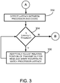
- undesirable latency between the PCM controller 104 and the signal processor 106 may be compensated by detecting the latency or delay in operations between the circuits, at 302, and determining whether a latency threshold is exceeded, at step 304. Extreme latencies may cause significant quality issues over and above periodic lost data problems caused, for example, by buffer overwrites. If the latency threshold is within limits, then operation resumes with the data receive step 202 of Figure 2 (via bubble "B").
- the relative position of the transmit buffer read and write pointers is adaptively adjusted to match the processor latency, at step 306. In one embodiment this is carried out by adjusting the position of the transmit write pointer WIT x in an iterative manner until the latency falls within limits. In some instances, this may cause a temporary data loss of the data residing in the buffer cell location(s) eliminated due to the adaptive adjustment of the transmit write pointer WIT x . While losing data is contrary to conventional wisdom, this has been determined to be more beneficial for optimal quality of service than keeping the data and tolerating the latency.
Claims (10)
- Verfahren zum Synchronisieren von Abläufen zwischen einem ersten Schaltkreis (104) und einem zweiten Schaltkreis (106), das Verfahren aufweisend:Schreiben (202) von Daten von dem ersten Schaltkreis (104) in einen ersten Ringpuffer (108) bei einer ersten Rate, der erste Ringpuffer (108) aufweisend eine fixierte Länge von Pufferelementen und jeweiligen Lese- und Schreibepufferanzeigen;Lesen (206) der gepufferten Daten von dem ersten Ringpuffer (108) in den zweiten Schaltkreis (106) bei einer zweiten Datenrate;Detektieren, durch den zweiten Schaltkreis (106), der jeweiligen Positionen der Lese- und Schreibepufferanzeigen;Dynamisches Anpassen (210) durch den zweiten Schaltkreis, einer relativen Position zwischen den Anzeigen um wenigstens einen vorherbestimmten minimalen Abstand zu erzwingen, wobei das dynamische Anpassen das selektive Addieren oder Löschen von Teilen von den Daten in oder von dem ersten Ringpuffer (108) aufweist;Schreiben von Sendedaten von dem zweiten Schaltkreis (106) in einen zweiten Ringpuffer (110) bei der zweiten Datenrate, der zweite Ringpuffer (110) aufweisend jeweilige Schreibe- und Lesezeiger;Lesen der gepufferten Sendedaten von dem zweiten Ringpuffer (110) in den ersten Schaltkreis (104) bei einer ersten Datenrate; undadaptives Anpassen durch den zweiten Schaltkreis (106), der Positionen von den zweiten Ringpufferlese- und schreibezeigern basierend auf einem Verzögerungsparameter.
- Verfahren nach Anspruch 1, wobei der Verzögerungsparameter eine Latenz im Ablauf von dem zweiten Schaltkreis (106) mit Bezug auf den ersten Schaltkreis (104) aufweist und adaptives Anpassen, aufweisend das adaptive Anpassen der relativen Position zwischen den zweiten Ringpufferlese- und schreibezeigern aufweist um die Latenz anzugleichen.
- Verfahren nach Anspruch 2, wobei der Schreibezeiger für den zweiten Ringpuffer (110) antwortet auf eine erste Zeitgebungsreferenz, die assoziiert ist mit dem zweiten Schaltkreis (106), und der Lesezeiger des zweiten Ringpuffers (110) antwortet auf eine zweite Zeitgebungsreferenz, die assoziiert ist mit dem ersten Schaltkreis (104).
- Verfahren nach Anspruch 3, wobei eine Phasendifferenz zwischen den ersten und zweiten Zeitgebungsreferenzen der Latenz entspricht.
- Verfahren nach Anspruch 3, wobei die erste Zeitgebungsreferenz eine Uhr aufweist, welche von Daten wiederhergestellt wird, welche von dem ersten Schaltkreis (104) empfangen werden und die zweite Zeitgebungsreferenz eine lokale Uhr aufweist, welche den zweiten Schaltkreis taktet.
- Integrierte Schaltkreisvorrichtung (102) aufweisend:einen ersten Schaltkreis (104), welcher auf eine erste Zeitgebungsreferenz antwortet;einen zweiten Schaltkreis (106), der auf eine zweite Zeitgebungsreferenz antwortet; undeinen Pufferschaltkreis (107) aufweisend einen Empfangsringpuffer (108) der betreibbar ist um Daten von dem ersten Schaltkreis (104) zu empfangen in Antwort auf einen Empfangsschreibezeiger, der Empfangsringpuffer (108) ist betreibbar um Daten an den zweiten Schaltkreis (106) zu liefern, in Antwort auf einen Empfangslesezeiger;wobei der zweite Schaltkreis (106) die relativen Positionen zwischen den Empfangslese- und schreibezeigern anpasst um einen vorherbestimmten minimalen Abstand dazwischen zu erzwingen, die integrierte Schaltkreisvorrichtung (102) weiterhin aufweisend:einen Senderingpuffer (110) zum Empfangen von Daten von dem zweiten Schaltkreis (106) in Antwort auf einen Sendeschreibezeiger und zum Liefern von Sendedaten an den ersten Schaltkreis (104) in Antwort auf einen Sendeschreibezeiger, wobei der Sendeschreibezeiger synchronisiert ist mit der zweiten Zeitgebungsreferenz und der Sendelesezeiger synchronisiert ist mit der ersten Zeitgebungsreferenz, wobei die Positionen der Senderingpufferlese- und schreibezeiger adaptiv angepasst werden, basierend auf einem Verzögerungsparameter.
- Integrierte Schaltkreisvorrichtung (102) nach Anspruch 6, wobei der erste Schaltkreis (104) ein Pulscode-modulation, PCM, Controller und der zweite Schaltkreis einen Soft-DSP-Schaltkreis aufweist.
- Integrierte Schaltkreisvorrichtung (102) nach Anspruch 6, wobei die erste Zeitgebungsreferenz ein wiederhergestelltes Taktsignal ist, welches von Daten wiederhergestellt wird, welche mit dem ersten Schaltkreis (104) assoziiert sind und die zweite Zeitgebungsreferenz ein lokales Taktsignal aufweist.
- Integrierte Schaltkreisvorrichtung (102) nach Anspruch 6, wobei der zweite Schaltkreis (106) aufweist:eine Logik, die betreibbar ist um die relativen Positionen zwischen den Sende-, Lese- und Schreibezeigern zu detektieren und um die relativen Positionen adaptiv anzupassen, basierend auf einem Schwellenwertniveau von Verzögerung, welches zwischen den Sende-, Lese- und Schreibezeigern detektiert wird.
- Integrierte Schaltkreisvorrichtung (102) nach Anspruch 9, wobei der zweite Schaltkreis (106) eine Latenz mit Bezug auf den ersten Schaltkreis (104) besitzt und die adaptive Anpassung den relativen Abstand zwischen den Sende-, Lese- und Schreibezeigern neu positioniert um die Latenz abzugleichen.
Applications Claiming Priority (1)
| Application Number | Priority Date | Filing Date | Title |
|---|---|---|---|
| PCT/CN2012/077071 WO2013189009A1 (en) | 2012-06-18 | 2012-06-18 | Adaptive offset synchronization of data based on ring buffers |
Publications (3)
| Publication Number | Publication Date |
|---|---|
| EP2862090A1 EP2862090A1 (de) | 2015-04-22 |
| EP2862090A4 EP2862090A4 (de) | 2015-12-30 |
| EP2862090B1 true EP2862090B1 (de) | 2017-11-08 |
Family
ID=49768000
Family Applications (1)
| Application Number | Title | Priority Date | Filing Date |
|---|---|---|---|
| EP12879587.9A Not-in-force EP2862090B1 (de) | 2012-06-18 | 2012-06-18 | Adaptive versetzte synchronisation von daten auf der basis von ringspeichern |
Country Status (6)
| Country | Link |
|---|---|
| US (1) | US9621331B2 (de) |
| EP (1) | EP2862090B1 (de) |
| JP (1) | JP6113839B2 (de) |
| CN (1) | CN104380273B (de) |
| IN (1) | IN2014MN02369A (de) |
| WO (1) | WO2013189009A1 (de) |
Families Citing this family (5)
| Publication number | Priority date | Publication date | Assignee | Title |
|---|---|---|---|---|
| CN107430578B (zh) * | 2015-03-30 | 2020-11-17 | 索尼半导体解决方案公司 | 异步接口 |
| CN107272822A (zh) * | 2017-06-16 | 2017-10-20 | 郑州云海信息技术有限公司 | 一种系统时钟监控方法及装置 |
| CN107423148A (zh) * | 2017-07-26 | 2017-12-01 | 广州路派电子科技有限公司 | 一种适用于多任务调度环境下的双缓冲协议数据分析系统 |
| CN107797956B (zh) | 2017-11-14 | 2019-04-23 | 深圳锐越微技术有限公司 | 双沿触发环形缓冲器及通信系统 |
| US11816110B2 (en) * | 2021-06-22 | 2023-11-14 | International Business Machines Corporation | Processing large query results in a database accelerator environment |
Family Cites Families (21)
| Publication number | Priority date | Publication date | Assignee | Title |
|---|---|---|---|---|
| JPS61191134A (ja) | 1985-02-19 | 1986-08-25 | Mitsubishi Electric Corp | プレジオクロナス整合装置 |
| JPH0458646A (ja) | 1990-06-28 | 1992-02-25 | Toshiba Corp | バッファ管理方式 |
| CN1095584C (zh) * | 1995-10-13 | 2002-12-04 | 盛群半导体股份有限公司 | 存储器存取之接口电路及存储器存取的方法 |
| SE509186C2 (sv) | 1996-06-25 | 1998-12-14 | Ericsson Telefon Ab L M | Anordning och metod vid behandling av redundanssignaler och ett telekommunikationssystem omfattande densamma |
| US6977897B1 (en) | 2000-05-08 | 2005-12-20 | Crossroads Systems, Inc. | System and method for jitter compensation in data transfers |
| CN1213577C (zh) * | 2001-03-22 | 2005-08-03 | 中兴通讯股份有限公司 | 一种在成帧器中实现高速率数据复接的方法 |
| JP3879547B2 (ja) | 2002-03-18 | 2007-02-14 | 三菱電機株式会社 | データ同期化装置 |
| US6799227B2 (en) * | 2003-01-06 | 2004-09-28 | Lsi Logic Corporation | Dynamic configuration of a time division multiplexing port and associated direct memory access controller |
| US7729790B1 (en) * | 2003-03-21 | 2010-06-01 | D2Audio Corporation | Phase alignment of audio output data in a multi-channel configuration |
| US7242736B2 (en) | 2003-05-15 | 2007-07-10 | Sun Microsystems, Inc. | Data transfer |
| US7234007B2 (en) * | 2003-09-15 | 2007-06-19 | Broadcom Corporation | Adjustable elasticity FIFO buffer have a number of storage cells equal to a frequency offset times a number of data units in a data stream |
| US7734674B2 (en) * | 2005-08-08 | 2010-06-08 | Freescale Semiconductor, Inc. | Fast fourier transform (FFT) architecture in a multi-mode wireless processing system |
| US7457913B2 (en) * | 2006-03-22 | 2008-11-25 | Infineon Technologies Ag | Finding a data pattern in a memory |
| US7657668B2 (en) | 2006-08-16 | 2010-02-02 | Qnx Software Systems (Wavemakers), Inc. | Clock synchronization of data streams |
| CN101212490A (zh) * | 2006-12-30 | 2008-07-02 | 财团法人工业技术研究院 | 储存装置控制器 |
| CN101296217B (zh) | 2007-04-24 | 2011-07-06 | 中芯国际集成电路制造(上海)有限公司 | 弹性缓冲装置 |
| JP2010160653A (ja) | 2009-01-07 | 2010-07-22 | Renesas Electronics Corp | リングバッファ回路及びその制御回路 |
| CN101930416B (zh) * | 2009-06-21 | 2013-05-29 | 先耀无线股份有限公司 | 硬件协助处理器间的沟通 |
| US8634023B2 (en) | 2009-07-21 | 2014-01-21 | Qualcomm Incorporated | System for video frame synchronization using sub-frame memories |
| JP5234845B2 (ja) | 2010-10-21 | 2013-07-10 | Necアクセステクニカ株式会社 | パケット送受信装置、方法及びプログラム |
| JP5681449B2 (ja) | 2010-11-02 | 2015-03-11 | ルネサスエレクトロニクス株式会社 | 情報処理装置及び携帯端末 |
-
2012
- 2012-06-18 JP JP2015516406A patent/JP6113839B2/ja active Active
- 2012-06-18 US US14/399,932 patent/US9621331B2/en not_active Expired - Fee Related
- 2012-06-18 IN IN2369MUN2014 patent/IN2014MN02369A/en unknown
- 2012-06-18 EP EP12879587.9A patent/EP2862090B1/de not_active Not-in-force
- 2012-06-18 CN CN201280074005.8A patent/CN104380273B/zh not_active Expired - Fee Related
- 2012-06-18 WO PCT/CN2012/077071 patent/WO2013189009A1/en active Application Filing
Non-Patent Citations (1)
| Title |
|---|
| None * |
Also Published As
| Publication number | Publication date |
|---|---|
| CN104380273B (zh) | 2017-10-24 |
| EP2862090A1 (de) | 2015-04-22 |
| JP2015528223A (ja) | 2015-09-24 |
| JP6113839B2 (ja) | 2017-04-12 |
| EP2862090A4 (de) | 2015-12-30 |
| WO2013189009A1 (en) | 2013-12-27 |
| CN104380273A (zh) | 2015-02-25 |
| US9621331B2 (en) | 2017-04-11 |
| US20150124841A1 (en) | 2015-05-07 |
| IN2014MN02369A (de) | 2015-08-14 |
Similar Documents
| Publication | Publication Date | Title |
|---|---|---|
| EP2862090B1 (de) | Adaptive versetzte synchronisation von daten auf der basis von ringspeichern | |
| EP0762655B1 (de) | Kommunikationssystem für eine Datenverarbeitungsanlage mit Ersetzung von fehlgeschlagenen Routinen durch Kompensationssignale | |
| JP6221328B2 (ja) | 受信装置、情報処理装置及びデータ受信方法 | |
| US6738917B2 (en) | Low latency synchronization of asynchronous data | |
| US9001954B2 (en) | Reception circuit, information processing device, and buffer control method | |
| US20170046298A1 (en) | Asynchronous first-in first-out buffer apparatus with active rate control and dynamic rate compensation and associated network device using the same | |
| KR101174234B1 (ko) | 직렬 데이터 수신 회로 장치 및 직렬 데이터 수신 방법 | |
| JP2011525093A (ja) | 周波数応答バス符号化 | |
| US6516420B1 (en) | Data synchronizer using a parallel handshaking pipeline wherein validity indicators generate and send acknowledgement signals to a different clock domain | |
| US10536260B2 (en) | Baseband integrated circuit for performing digital communication with radio frequency integrated circuit and device including the same | |
| JP2017130930A (ja) | リングバッファに基づいたデータの適応オフセット同期(adaptive offset synchronization) | |
| US7605737B2 (en) | Data encoding in a clocked data interface | |
| US7697555B1 (en) | Fibre channel SERDES with elastic transmitter FIFO | |
| EP2075707B1 (de) | Verfahren zur Übertragung von Audioströmen und Audioströmungsübertragungssystem dafür | |
| JP5545146B2 (ja) | シリアル通信システム | |
| CN115774469A (zh) | 时序调整电路、时序不对称消除方法及接收电路 | |
| KR100907805B1 (ko) | 에이엑스아이 매트릭스 시스템과 에이에이치비 마스터시스템간의 데이터 전송을 위한 랩퍼 장치 및 제어 방법 | |
| TWI484333B (zh) | 彈性緩衝器模組及傳輸介面之彈性緩衝方法 | |
| EP1911188B1 (de) | Asynchroner datenpuffer | |
| CN110535619B (zh) | 多速率数字传感器同步 | |
| WO2023159415A1 (en) | Adaptive low-power signaling to enable link signal error recovery without increased link clock rates | |
| US20230136070A1 (en) | Methods and apparatus to synchronize signals in energy efficient ethernet protocols | |
| US7042932B1 (en) | Synchronization detection architecture for serial data communication | |
| US7133946B2 (en) | Mechanism to repeat signals across an unrelated link |
Legal Events
| Date | Code | Title | Description |
|---|---|---|---|
| PUAI | Public reference made under article 153(3) epc to a published international application that has entered the european phase |
Free format text: ORIGINAL CODE: 0009012 |
|
| 17P | Request for examination filed |
Effective date: 20141203 |
|
| AK | Designated contracting states |
Kind code of ref document: A1 Designated state(s): AL AT BE BG CH CY CZ DE DK EE ES FI FR GB GR HR HU IE IS IT LI LT LU LV MC MK MT NL NO PL PT RO RS SE SI SK SM TR |
|
| AX | Request for extension of the european patent |
Extension state: BA ME |
|
| DAX | Request for extension of the european patent (deleted) | ||
| RA4 | Supplementary search report drawn up and despatched (corrected) |
Effective date: 20151130 |
|
| RIC1 | Information provided on ipc code assigned before grant |
Ipc: G06F 13/28 20060101AFI20151124BHEP Ipc: G06F 5/14 20060101ALI20151124BHEP Ipc: G06F 5/12 20060101ALI20151124BHEP |
|
| GRAP | Despatch of communication of intention to grant a patent |
Free format text: ORIGINAL CODE: EPIDOSNIGR1 |
|
| INTG | Intention to grant announced |
Effective date: 20170516 |
|
| GRAS | Grant fee paid |
Free format text: ORIGINAL CODE: EPIDOSNIGR3 |
|
| GRAA | (expected) grant |
Free format text: ORIGINAL CODE: 0009210 |
|
| AK | Designated contracting states |
Kind code of ref document: B1 Designated state(s): AL AT BE BG CH CY CZ DE DK EE ES FI FR GB GR HR HU IE IS IT LI LT LU LV MC MK MT NL NO PL PT RO RS SE SI SK SM TR |
|
| REG | Reference to a national code |
Ref country code: GB Ref legal event code: FG4D |
|
| REG | Reference to a national code |
Ref country code: CH Ref legal event code: EP Ref country code: AT Ref legal event code: REF Ref document number: 944788 Country of ref document: AT Kind code of ref document: T Effective date: 20171115 |
|
| REG | Reference to a national code |
Ref country code: IE Ref legal event code: FG4D |
|
| REG | Reference to a national code |
Ref country code: DE Ref legal event code: R096 Ref document number: 602012039654 Country of ref document: DE |
|
| REG | Reference to a national code |
Ref country code: NL Ref legal event code: MP Effective date: 20171108 |
|
| REG | Reference to a national code |
Ref country code: LT Ref legal event code: MG4D |
|
| REG | Reference to a national code |
Ref country code: AT Ref legal event code: MK05 Ref document number: 944788 Country of ref document: AT Kind code of ref document: T Effective date: 20171108 |
|
| PG25 | Lapsed in a contracting state [announced via postgrant information from national office to epo] |
Ref country code: NO Free format text: LAPSE BECAUSE OF FAILURE TO SUBMIT A TRANSLATION OF THE DESCRIPTION OR TO PAY THE FEE WITHIN THE PRESCRIBED TIME-LIMIT Effective date: 20180208 Ref country code: SE Free format text: LAPSE BECAUSE OF FAILURE TO SUBMIT A TRANSLATION OF THE DESCRIPTION OR TO PAY THE FEE WITHIN THE PRESCRIBED TIME-LIMIT Effective date: 20171108 Ref country code: NL Free format text: LAPSE BECAUSE OF FAILURE TO SUBMIT A TRANSLATION OF THE DESCRIPTION OR TO PAY THE FEE WITHIN THE PRESCRIBED TIME-LIMIT Effective date: 20171108 Ref country code: LT Free format text: LAPSE BECAUSE OF FAILURE TO SUBMIT A TRANSLATION OF THE DESCRIPTION OR TO PAY THE FEE WITHIN THE PRESCRIBED TIME-LIMIT Effective date: 20171108 Ref country code: FI Free format text: LAPSE BECAUSE OF FAILURE TO SUBMIT A TRANSLATION OF THE DESCRIPTION OR TO PAY THE FEE WITHIN THE PRESCRIBED TIME-LIMIT Effective date: 20171108 Ref country code: ES Free format text: LAPSE BECAUSE OF FAILURE TO SUBMIT A TRANSLATION OF THE DESCRIPTION OR TO PAY THE FEE WITHIN THE PRESCRIBED TIME-LIMIT Effective date: 20171108 |
|
| REG | Reference to a national code |
Ref country code: FR Ref legal event code: PLFP Year of fee payment: 7 |
|
| PG25 | Lapsed in a contracting state [announced via postgrant information from national office to epo] |
Ref country code: RS Free format text: LAPSE BECAUSE OF FAILURE TO SUBMIT A TRANSLATION OF THE DESCRIPTION OR TO PAY THE FEE WITHIN THE PRESCRIBED TIME-LIMIT Effective date: 20171108 Ref country code: LV Free format text: LAPSE BECAUSE OF FAILURE TO SUBMIT A TRANSLATION OF THE DESCRIPTION OR TO PAY THE FEE WITHIN THE PRESCRIBED TIME-LIMIT Effective date: 20171108 Ref country code: BG Free format text: LAPSE BECAUSE OF FAILURE TO SUBMIT A TRANSLATION OF THE DESCRIPTION OR TO PAY THE FEE WITHIN THE PRESCRIBED TIME-LIMIT Effective date: 20180208 Ref country code: GR Free format text: LAPSE BECAUSE OF FAILURE TO SUBMIT A TRANSLATION OF THE DESCRIPTION OR TO PAY THE FEE WITHIN THE PRESCRIBED TIME-LIMIT Effective date: 20180209 Ref country code: HR Free format text: LAPSE BECAUSE OF FAILURE TO SUBMIT A TRANSLATION OF THE DESCRIPTION OR TO PAY THE FEE WITHIN THE PRESCRIBED TIME-LIMIT Effective date: 20171108 Ref country code: IS Free format text: LAPSE BECAUSE OF FAILURE TO SUBMIT A TRANSLATION OF THE DESCRIPTION OR TO PAY THE FEE WITHIN THE PRESCRIBED TIME-LIMIT Effective date: 20180308 Ref country code: AT Free format text: LAPSE BECAUSE OF FAILURE TO SUBMIT A TRANSLATION OF THE DESCRIPTION OR TO PAY THE FEE WITHIN THE PRESCRIBED TIME-LIMIT Effective date: 20171108 |
|
| PG25 | Lapsed in a contracting state [announced via postgrant information from national office to epo] |
Ref country code: SK Free format text: LAPSE BECAUSE OF FAILURE TO SUBMIT A TRANSLATION OF THE DESCRIPTION OR TO PAY THE FEE WITHIN THE PRESCRIBED TIME-LIMIT Effective date: 20171108 Ref country code: CZ Free format text: LAPSE BECAUSE OF FAILURE TO SUBMIT A TRANSLATION OF THE DESCRIPTION OR TO PAY THE FEE WITHIN THE PRESCRIBED TIME-LIMIT Effective date: 20171108 Ref country code: CY Free format text: LAPSE BECAUSE OF FAILURE TO SUBMIT A TRANSLATION OF THE DESCRIPTION OR TO PAY THE FEE WITHIN THE PRESCRIBED TIME-LIMIT Effective date: 20171108 Ref country code: EE Free format text: LAPSE BECAUSE OF FAILURE TO SUBMIT A TRANSLATION OF THE DESCRIPTION OR TO PAY THE FEE WITHIN THE PRESCRIBED TIME-LIMIT Effective date: 20171108 Ref country code: DK Free format text: LAPSE BECAUSE OF FAILURE TO SUBMIT A TRANSLATION OF THE DESCRIPTION OR TO PAY THE FEE WITHIN THE PRESCRIBED TIME-LIMIT Effective date: 20171108 |
|
| REG | Reference to a national code |
Ref country code: DE Ref legal event code: R097 Ref document number: 602012039654 Country of ref document: DE |
|
| PG25 | Lapsed in a contracting state [announced via postgrant information from national office to epo] |
Ref country code: RO Free format text: LAPSE BECAUSE OF FAILURE TO SUBMIT A TRANSLATION OF THE DESCRIPTION OR TO PAY THE FEE WITHIN THE PRESCRIBED TIME-LIMIT Effective date: 20171108 Ref country code: IT Free format text: LAPSE BECAUSE OF FAILURE TO SUBMIT A TRANSLATION OF THE DESCRIPTION OR TO PAY THE FEE WITHIN THE PRESCRIBED TIME-LIMIT Effective date: 20171108 Ref country code: SM Free format text: LAPSE BECAUSE OF FAILURE TO SUBMIT A TRANSLATION OF THE DESCRIPTION OR TO PAY THE FEE WITHIN THE PRESCRIBED TIME-LIMIT Effective date: 20171108 Ref country code: PL Free format text: LAPSE BECAUSE OF FAILURE TO SUBMIT A TRANSLATION OF THE DESCRIPTION OR TO PAY THE FEE WITHIN THE PRESCRIBED TIME-LIMIT Effective date: 20171108 |
|
| PGFP | Annual fee paid to national office [announced via postgrant information from national office to epo] |
Ref country code: FR Payment date: 20180516 Year of fee payment: 7 |
|
| PLBE | No opposition filed within time limit |
Free format text: ORIGINAL CODE: 0009261 |
|
| STAA | Information on the status of an ep patent application or granted ep patent |
Free format text: STATUS: NO OPPOSITION FILED WITHIN TIME LIMIT |
|
| 26N | No opposition filed |
Effective date: 20180809 |
|
| PGFP | Annual fee paid to national office [announced via postgrant information from national office to epo] |
Ref country code: GB Payment date: 20180403 Year of fee payment: 7 |
|
| PG25 | Lapsed in a contracting state [announced via postgrant information from national office to epo] |
Ref country code: SI Free format text: LAPSE BECAUSE OF FAILURE TO SUBMIT A TRANSLATION OF THE DESCRIPTION OR TO PAY THE FEE WITHIN THE PRESCRIBED TIME-LIMIT Effective date: 20171108 |
|
| REG | Reference to a national code |
Ref country code: CH Ref legal event code: PL |
|
| REG | Reference to a national code |
Ref country code: BE Ref legal event code: MM Effective date: 20180630 |
|
| REG | Reference to a national code |
Ref country code: IE Ref legal event code: MM4A |
|
| PG25 | Lapsed in a contracting state [announced via postgrant information from national office to epo] |
Ref country code: LU Free format text: LAPSE BECAUSE OF NON-PAYMENT OF DUE FEES Effective date: 20180618 Ref country code: MC Free format text: LAPSE BECAUSE OF FAILURE TO SUBMIT A TRANSLATION OF THE DESCRIPTION OR TO PAY THE FEE WITHIN THE PRESCRIBED TIME-LIMIT Effective date: 20171108 |
|
| PG25 | Lapsed in a contracting state [announced via postgrant information from national office to epo] |
Ref country code: IE Free format text: LAPSE BECAUSE OF NON-PAYMENT OF DUE FEES Effective date: 20180618 Ref country code: CH Free format text: LAPSE BECAUSE OF NON-PAYMENT OF DUE FEES Effective date: 20180630 Ref country code: LI Free format text: LAPSE BECAUSE OF NON-PAYMENT OF DUE FEES Effective date: 20180630 |
|
| PG25 | Lapsed in a contracting state [announced via postgrant information from national office to epo] |
Ref country code: BE Free format text: LAPSE BECAUSE OF NON-PAYMENT OF DUE FEES Effective date: 20180630 |
|
| PGFP | Annual fee paid to national office [announced via postgrant information from national office to epo] |
Ref country code: DE Payment date: 20190515 Year of fee payment: 8 |
|
| PG25 | Lapsed in a contracting state [announced via postgrant information from national office to epo] |
Ref country code: MT Free format text: LAPSE BECAUSE OF NON-PAYMENT OF DUE FEES Effective date: 20180618 |
|
| GBPC | Gb: european patent ceased through non-payment of renewal fee |
Effective date: 20190618 |
|
| PG25 | Lapsed in a contracting state [announced via postgrant information from national office to epo] |
Ref country code: TR Free format text: LAPSE BECAUSE OF FAILURE TO SUBMIT A TRANSLATION OF THE DESCRIPTION OR TO PAY THE FEE WITHIN THE PRESCRIBED TIME-LIMIT Effective date: 20171108 |
|
| PG25 | Lapsed in a contracting state [announced via postgrant information from national office to epo] |
Ref country code: GB Free format text: LAPSE BECAUSE OF NON-PAYMENT OF DUE FEES Effective date: 20190618 |
|
| PG25 | Lapsed in a contracting state [announced via postgrant information from national office to epo] |
Ref country code: PT Free format text: LAPSE BECAUSE OF FAILURE TO SUBMIT A TRANSLATION OF THE DESCRIPTION OR TO PAY THE FEE WITHIN THE PRESCRIBED TIME-LIMIT Effective date: 20171108 |
|
| PG25 | Lapsed in a contracting state [announced via postgrant information from national office to epo] |
Ref country code: FR Free format text: LAPSE BECAUSE OF NON-PAYMENT OF DUE FEES Effective date: 20190630 Ref country code: MK Free format text: LAPSE BECAUSE OF NON-PAYMENT OF DUE FEES Effective date: 20171108 Ref country code: HU Free format text: LAPSE BECAUSE OF FAILURE TO SUBMIT A TRANSLATION OF THE DESCRIPTION OR TO PAY THE FEE WITHIN THE PRESCRIBED TIME-LIMIT; INVALID AB INITIO Effective date: 20120618 |
|
| PG25 | Lapsed in a contracting state [announced via postgrant information from national office to epo] |
Ref country code: AL Free format text: LAPSE BECAUSE OF FAILURE TO SUBMIT A TRANSLATION OF THE DESCRIPTION OR TO PAY THE FEE WITHIN THE PRESCRIBED TIME-LIMIT Effective date: 20171108 |
|
| REG | Reference to a national code |
Ref country code: DE Ref legal event code: R119 Ref document number: 602012039654 Country of ref document: DE |
|
| PG25 | Lapsed in a contracting state [announced via postgrant information from national office to epo] |
Ref country code: DE Free format text: LAPSE BECAUSE OF NON-PAYMENT OF DUE FEES Effective date: 20210101 |