EP2860762A1 - High voltage junction field effect transistor - Google Patents
High voltage junction field effect transistor Download PDFInfo
- Publication number
- EP2860762A1 EP2860762A1 EP13804198.3A EP13804198A EP2860762A1 EP 2860762 A1 EP2860762 A1 EP 2860762A1 EP 13804198 A EP13804198 A EP 13804198A EP 2860762 A1 EP2860762 A1 EP 2860762A1
- Authority
- EP
- European Patent Office
- Prior art keywords
- conductivity type
- region
- heavily doped
- high voltage
- doped region
- Prior art date
- Legal status (The legal status is an assumption and is not a legal conclusion. Google has not performed a legal analysis and makes no representation as to the accuracy of the status listed.)
- Granted
Links
Images


Classifications
-
- H—ELECTRICITY
- H10—SEMICONDUCTOR DEVICES; ELECTRIC SOLID-STATE DEVICES NOT OTHERWISE PROVIDED FOR
- H10D—INORGANIC ELECTRIC SEMICONDUCTOR DEVICES
- H10D30/00—Field-effect transistors [FET]
- H10D30/80—FETs having rectifying junction gate electrodes
- H10D30/83—FETs having PN junction gate electrodes
-
- H—ELECTRICITY
- H10—SEMICONDUCTOR DEVICES; ELECTRIC SOLID-STATE DEVICES NOT OTHERWISE PROVIDED FOR
- H10D—INORGANIC ELECTRIC SEMICONDUCTOR DEVICES
- H10D62/00—Semiconductor bodies, or regions thereof, of devices having potential barriers
- H10D62/10—Shapes, relative sizes or dispositions of the regions of the semiconductor bodies; Shapes of the semiconductor bodies
- H10D62/17—Semiconductor regions connected to electrodes not carrying current to be rectified, amplified or switched, e.g. channel regions
- H10D62/213—Channel regions of field-effect devices
- H10D62/221—Channel regions of field-effect devices of FETs
- H10D62/328—Channel regions of field-effect devices of FETs having PN junction gates
-
- H—ELECTRICITY
- H10—SEMICONDUCTOR DEVICES; ELECTRIC SOLID-STATE DEVICES NOT OTHERWISE PROVIDED FOR
- H10D—INORGANIC ELECTRIC SEMICONDUCTOR DEVICES
- H10D62/00—Semiconductor bodies, or regions thereof, of devices having potential barriers
- H10D62/10—Shapes, relative sizes or dispositions of the regions of the semiconductor bodies; Shapes of the semiconductor bodies
- H10D62/17—Semiconductor regions connected to electrodes not carrying current to be rectified, amplified or switched, e.g. channel regions
- H10D62/343—Gate regions of field-effect devices having PN junction gates
-
- H—ELECTRICITY
- H10—SEMICONDUCTOR DEVICES; ELECTRIC SOLID-STATE DEVICES NOT OTHERWISE PROVIDED FOR
- H10D—INORGANIC ELECTRIC SEMICONDUCTOR DEVICES
- H10D64/00—Electrodes of devices having potential barriers
- H10D64/111—Field plates
-
- H—ELECTRICITY
- H10—SEMICONDUCTOR DEVICES; ELECTRIC SOLID-STATE DEVICES NOT OTHERWISE PROVIDED FOR
- H10D—INORGANIC ELECTRIC SEMICONDUCTOR DEVICES
- H10D62/00—Semiconductor bodies, or regions thereof, of devices having potential barriers
- H10D62/10—Shapes, relative sizes or dispositions of the regions of the semiconductor bodies; Shapes of the semiconductor bodies
- H10D62/113—Isolations within a component, i.e. internal isolations
- H10D62/115—Dielectric isolations, e.g. air gaps
- H10D62/116—Dielectric isolations, e.g. air gaps adjoining the input or output regions of field-effect devices, e.g. adjoining source or drain regions
-
- H—ELECTRICITY
- H10—SEMICONDUCTOR DEVICES; ELECTRIC SOLID-STATE DEVICES NOT OTHERWISE PROVIDED FOR
- H10D—INORGANIC ELECTRIC SEMICONDUCTOR DEVICES
- H10D62/00—Semiconductor bodies, or regions thereof, of devices having potential barriers
- H10D62/10—Shapes, relative sizes or dispositions of the regions of the semiconductor bodies; Shapes of the semiconductor bodies
- H10D62/13—Semiconductor regions connected to electrodes carrying current to be rectified, amplified or switched, e.g. source or drain regions
- H10D62/149—Source or drain regions of field-effect devices
Definitions
- the present invention relates to a device structure of a field effect transistor, and more particularly, relates to a JFET (Junction Field Effect Transistor) applied in high voltage, which belongs to a field of semiconductor producing.
- JFET Joint Field Effect Transistor
- Field effect transistors are widely employed to design various simulation circuits, for example, applied to an amplifier circuit, a biasing circuit or a step-down circuit, a starting circuit, or a variable resistance, and so on.
- As an emerging demand for high voltage devices how to improve breakdown voltage of various kinds of field effect transistors has become a design target of high voltage field effect transistor.
- a DMOS Double-diffused MOS
- characteristics such as a high current drive capacity, a low on-resistance, and a high breakdown voltage, such that DMOS is widely employed by power devices.
- LDMOSFET Longteral Double-diffused MOSFET
- the DMOS device is provided with a drift region between an active region and an drain region, and a impurity concentration of the drift region is relative low.
- the LDMOS When the LDMOS is connected to a high voltage, because the drift region has a high impendence, the drift region can withstand a relative high voltage.
- the polycrystalline layer or metal layer of the LDMOS extends above an oxygen region of the drift region, and serves as a field electrode plate, thereby weakening a surface electric field of the drift region, and benefiting for improving a breakdown voltage.
- the drain electrode voltage of the JFET is applied to the PN junction of the drain electrode and the gate electrode, and the breaking point is normally located within the body, not on the surface. So the breakdown voltage of the JFET cannot be improved either by a filed electrode or by other types. So, the conventional JFET is limited by PN junction, and the breakdown voltage is about 20 ⁇ 30 volts, thereby limiting an application of JFET in high voltage field.
- the technical problem to be solved by the present invention to provide a high voltage JFET having a high breakdown voltage and being compatible with CMOS/LDMOS integrated circuit.
- the second conductivity type channel layer is a second conductivity type implantation layer formed by ions implantation.
- the field electrode plate is a polycrystalline layer or a metallic layer.
- the high voltage field effect transistor is provided with a second conductivity type well region at opposite sides thereof, and a second conductivity type deep well region is provided beneath the first conductivity type epitaxial layer to isolate the high voltage field effect transistor.
- a high voltage bearing structure is provided at a side of the second conductivity type drift region opposite to the first conductivity type well region.
- the first conductivity type is P type
- the second conductivity type is N type
- the first conductivity type is N type
- the second conductivity type is P type
- a high voltage junction field effect transistor includes:
- the second conductivity type channel layer is a second conductivity type implantation layer formed by ions implantation.
- the field electrode plate is a polycrystalline layer or a metallic layer.
- the high voltage field effect transistor is provided with a second conductivity type well region at opposite sides thereof, and a second conductivity type deep well region is provided beneath the first conductivity type epitaxial layer to isolate the high voltage field effect transistor.
- the first conductivity type is P type
- the second conductivity type is N type
- the first conductivity type is N type
- the second conductivity type is P type
- the high voltage JFET of the present invention draws the high voltage bearing structures of LDMOS for reference, and arranges the channel on an surface of the epitaxial layer, employing RESURF principle to greatly enhance a breakdown voltage of the JFET.
- the pinch-off voltage of the high voltage JFET can be adjusted by controlling the implantation conditions of the channel implantation layer.
- the producing technology of the high voltage JFET is compatible with conventional CMOS/LDMOS integrated circuit producing technology, so as to meet a requirement of high voltage semiconductor integrated circuit producing technology.
- the breakdown voltage of the conventional JFET thereof is about 20 ⁇ 30 volts.
- the present invention provides a high voltage JFET adapted to a higher input voltage, and compatible with CMOS/LDMOS integrated circuit producing technology.
- the device structure is specifically described hereinafter with reference to drawings.
- a high voltage JFET includes: a semiconductor substrate provided with a first conductivity type epitaxial layer 100; a second conductivity type drift region 110 located on the first conductivity type epitaxial layer 100; a second conductivity type drain heavily doped region 120 located in the second conductivity type drift region 110; a drain terminal oxygen region 130 located on the second conductivity type drift region 110 and at a side of the second conductivity type drain heavily doped region 120; a first conductivity type well region 140 located at a side of the second conductivity type drift region 110 and isolated from the second conductivity type drift region 110 by the first conductivity type epitaxial layer 100; a second conductivity type source heavily doped region 150 and a first conductivity type gate heavily doped region 160 located on the first conductivity type well region 140, a gate source terminal oxygen region 170 located between the second conductivity type source heavily doped region 150 and the first conductivity type gate heavily doped region 160 isolating above two regions 150, 160; a second conductivity type channel layer 180 located between the second conductivity type channel layer 180 located
- the device When the first conductivity type is selected as P type, the second conductivity type is selected as N type, then the device is an N channel JFET. When the first conductivity type is selected as N type, the second conductivity type is selected as P type, then the device is a P channel JFET.
- the drain electrode D, the source electrode S, the gate electrode G can be led out from metal wiring, it is well known for a person skilled in the art, specific details are not described herein.
- the gate electrode G is connected to the first conductivity type well region 140 via the first conductivity type gate heavily doped region 160, such that a depletion region between the first conductivity type well region 140 and the second conductivity type channel layer 180 can be affected by a gate electrode voltage, thereby controlling the current and on-off of the JFET.
- the second conductivity type channel layer 180 is a second conductivity type implantation layer formed by ions implantation, the pinch-off voltage of the field effect transistor can be adjusted by controlling the implantation conditions.
- the drain terminal of the JFET draws the high voltage bearing structures of LDMOS for reference, and is provided with the second conductivity type drift region 110, the drain terminal oxygen region 130, and the field electrode plate 190 extends to a part of the surface of the drain terminal oxygen region 130, and the channel is disposed on an surface of the epitaxial layer, employing RESURF principle to greatly enhance breakdown voltage of the JFET.
- the field electrode plate 190 can be a polycrystalline layer or a metallic layer.
- the field electrode plate 190 is a polycrystalline layer.
- the field electrode plate 190 is connected to the source electrode S to keep a same potential.
- the pinch-off voltage can be only controlled by the depletion region between the first conductivity type well region 140 and the second conductivity type channel layer 180. If the potential of the field electrode plate 190 is floating connected, the induction potential may cause a fluctuation of the pinch-off voltage. If the field electrode plate 190 is connected to the gate electrode G, i. e the first conductivity type well region 140, then a reverse biasing generated thereby is easy to exhaust charges of the second conductivity type drift region 110 on the portion A of FIG. 1 , causing the pinch-off voltage to be out of control of the technology conditions of the second conductivity type channel layer 180, and transistor may enter cutoff region prematurely.
- the high voltage field effect transistor may be provided with a second conductivity type well region 101 at opposite sides thereof, and a second conductivity type deep well regions 102 beneath the first conductivity type epitaxial layer 100, thereby forming an isolation structure to isolate the high voltage field effect transistor.
- a high voltage is applied to the drain electrode D of the high voltage JFET, a high voltage bearing structure such as well regions with low concentration and large size, i. e conventional well isolation structures may be provided at a side of the second conductivity type drift region 110 opposite to the first conductivity type well region 140, thereby avoiding the affection to surrounding devices raised by the JFET when applied with high voltage.
- another one high voltage JFET includes: a semiconductor substrate provided with a first conductivity type epitaxial layer 200; a second conductivity type drift region 210 located on the first conductivity type epitaxial layer 200; a second conductivity type drain heavily doped region 220 located in the second conductivity type drift region 210; a first drain terminal oxygen region 230 and a second drain terminal oxygen region 2300 located at opposite sides of the second conductivity type drain heavily doped region 220, and both the oxygen regions 230, 2300 being positioned on the second conductivity type drift region 210; a first first conductivity type well region 240 and a second first conductivity type well region 2400 located at opposite sides of the second conductivity type drift region 210, and both the well regions 240, 2400 being isolated from the second conductivity type drift region 210 by the first conductivity type epitaxial layer 200; a first second conductivity type source heavily doped region 260 and a first first conductivity type gate heavily doped region 250 located in the first first conductivity type well region
- the second conductivity type is selected as N type, thus the device is a N channel JFET;
- the first conductivity type is selected as N type, the second conductivity type is selected as P type, thus the device is a P channel JFET.
- the drain electrode D, the source electrode S, the gate electrode G can be led out from metal wiring, it is well known for a person skilled in the art, specific details are not described herein.
- both of the first second conductivity type channel layer 280 and the second second conductivity type channel layer 280 are second conductivity type implantation layers formed by ions implantation.
- the field electrode plate 190 can be a polycrystalline layer or a metal layer.
- the field electrode plate 190 is a polycrystalline layer.
- the high voltage field effect transistor may be provided two second conductivity type well regions 201 at opposite sides thereof, and a second conductivity type deep well regions 202 beneath the first conductivity type epitaxial layer 200, thereby isolating the high voltage field effect transistor.
- FIG. 3 is a characteristic graph of drain electrode current-gate source voltage of Id-Vgs
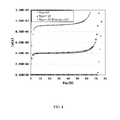
- FIG. 4 is a characteristic graph of drain electrode current-drain source electrode voltages of Id-Vds, the pinch-off voltage thereof is about -6 volts, the breakdown voltages thereof are all above 50 volts.
- the high voltage JFET provided by the present invention not only meets a requirement of high voltage bearing, but also provides good JFET IV characters, and is compatible with CMOS/LDMOS integrated circuit producing technology, therefore it is easy for integration.
Landscapes
- Insulated Gate Type Field-Effect Transistor (AREA)
- Junction Field-Effect Transistors (AREA)
Abstract
Description
- The present invention relates to a device structure of a field effect transistor, and more particularly, relates to a JFET (Junction Field Effect Transistor) applied in high voltage, which belongs to a field of semiconductor producing.
- Field effect transistors are widely employed to design various simulation circuits, for example, applied to an amplifier circuit, a biasing circuit or a step-down circuit, a starting circuit, or a variable resistance, and so on. As an emerging demand for high voltage devices, how to improve breakdown voltage of various kinds of field effect transistors has become a design target of high voltage field effect transistor.
- For MOSFET (Metal-Oxide-Semiconductor Field Effect Transistor), a DMOS (Double-diffused MOS) employing a planar diffusion technology is provided with characteristics such as a high current drive capacity, a low on-resistance, and a high breakdown voltage, such that DMOS is widely employed by power devices. Wherein, because LDMOSFET (Lateral Double-diffused MOSFET) is more compatible with CMOS technology, such that DMOS is widely employed. Normally, the DMOS device is provided with a drift region between an active region and an drain region, and a impurity concentration of the drift region is relative low. When the LDMOS is connected to a high voltage, because the drift region has a high impendence, the drift region can withstand a relative high voltage. In addition, the polycrystalline layer or metal layer of the LDMOS extends above an oxygen region of the drift region, and serves as a field electrode plate, thereby weakening a surface electric field of the drift region, and benefiting for improving a breakdown voltage.
- For JFET, it is different from the LDMOSFET, the drain electrode voltage of the JFET is applied to the PN junction of the drain electrode and the gate electrode, and the breaking point is normally located within the body, not on the surface. So the breakdown voltage of the JFET cannot be improved either by a filed electrode or by other types. So, the conventional JFET is limited by PN junction, and the breakdown voltage is about 20∼30 volts, thereby limiting an application of JFET in high voltage field.
- However, for emerging high voltage semiconductor integrated circuit technology, not only high voltage MOS transistor, but also high voltage JFET having high breakdown voltage and being compatible with CMOS/LDMOS integrated circuit producing technology are required, so as to meet a requirement of chips such as power management chips.
- The technical problem to be solved by the present invention to provide a high voltage JFET having a high breakdown voltage and being compatible with CMOS/LDMOS integrated circuit.
- In order to solve above technology problems, solutions are adopted by the present invention as follows:
- A high voltage junction field effect transistor includes:
- a semiconductor substrate provided with a first conductivity type epitaxial layer ;
- a second conductivity type drift region located on the first conductivity type epitaxial layer;
- a second conductivity type drain heavily doped region located in the second conductivity type drift region;
- a drain terminal oxygen region located on the second conductivity type drift region and at a side of the second conductivity type drain heavily doped region;
- a first conductivity type well region located at a side of the second conductivity type drift region, the first conductivity type well region being isolated from the second conductivity type drift region by the first conductivity type epitaxial layer;
- a second conductivity type source heavily doped region and a first conductivity type gate heavily doped region located on the first conductivity type well region, and a gate source terminal oxygen region being provided between the second conductivity type source heavily doped region and the first conductivity type gate heavily doped region to isolate the second conductivity type source heavily doped region from the first conductivity type gate heavily doped region;
- a second conductivity type channel layer located between the second conductivity type source heavily doped region and the second conductivity type drift region;
- a field electrode plate located on the second conductivity type channel layer, the field electrode plate extending to a part of the surface of the drain terminal oxygen region, a dielectric layer being provided between the field electrode plate and the second conductivity type channel layer, and also between the field electrode plate and the second conductivity type drift region;
- wherein a drain electrode electrically is led out from the second conductivity type drain heavily doped region; a source electrode electrically is led out from a connection of the field electrode plate and the second conductivity type source heavily doped region; and a gate electrode electrically is led out from the first conductivity type gate heavily doped region.
- In a preferred embodiment, the second conductivity type channel layer is a second conductivity type implantation layer formed by ions implantation.
- In a preferred embodiment, the field electrode plate is a polycrystalline layer or a metallic layer.
- In a preferred embodiment, the high voltage field effect transistor is provided with a second conductivity type well region at opposite sides thereof, and a second conductivity type deep well region is provided beneath the first conductivity type epitaxial layer to isolate the high voltage field effect transistor.
- In a preferred embodiment, a high voltage bearing structure is provided at a side of the second conductivity type drift region opposite to the first conductivity type well region.
- In a preferred embodiment, the first conductivity type is P type, the second conductivity type is N type.
- In a preferred embodiment, the first conductivity type is N type, the second conductivity type is P type.
- A high voltage junction field effect transistor according to another embodiment, includes:
- a semiconductor substrate provided with a first conductivity type epitaxial layer;
- a second conductivity type drift region located on the first conductivity type epitaxial layer;
- a second conductivity type drain heavily doped region located in the second conductivity type drift region;
- two drain terminal oxygen regions located at opposite sides of the second conductivity type drain heavily doped region, and both positioned on the second conductivity type drift region;
- two first conductivity type well regions located at opposite sides of the second conductivity type drift region, and each first conductivity type well region being isolated from the second conductivity type drift region by the first conductivity type epitaxial layer;
- a second conductivity type source heavily doped region and a first conductivity type gate heavily doped region in each first conductivity type well region, a gate source terminal oxygen region being provided between the second conductivity type source heavily doped region and the first conductivity type gate heavily doped region to isolate the second conductivity type source heavily doped region from the first conductivity type gate heavily doped region;
- two first second conductivity type channel layers each located between one second conductivity type source heavily doped region and the second conductivity type drift region;
- two field electrode plates respectively located on the two second conductivity type channel layers, each field electrode plate extending to a part of the surface of corresponding drain terminal oxygen region, and a dielectric layer being provided between the field electrode plate and the second conductivity type channel layer, the dielectric layer also located between the field electrode plate and the second conductivity type drift region;
- wherein, a drain electrode electrically is led out from the two second conductivity type drain heavily doped region; a source electrode electrically is led out from connections of the two field electrode plates at opposite sides of the drain electrode and the two second conductivity type source heavily doped regions; and a gate electrode electrically is led out from a connection of the two first conductivity type gate heavily doped regions at opposite sides of the drain electrode.
- In a preferred embodiment, the second conductivity type channel layer is a second conductivity type implantation layer formed by ions implantation.
- In a preferred embodiment, the field electrode plate is a polycrystalline layer or a metallic layer.
- In a preferred embodiment, the high voltage field effect transistor is provided with a second conductivity type well region at opposite sides thereof, and a second conductivity type deep well region is provided beneath the first conductivity type epitaxial layer to isolate the high voltage field effect transistor.
- In a preferred embodiment, the first conductivity type is P type, the second conductivity type is N type.
- In a preferred embodiment, the first conductivity type is N type, the second conductivity type is P type.
- The high voltage JFET of the present invention draws the high voltage bearing structures of LDMOS for reference, and arranges the channel on an surface of the epitaxial layer, employing RESURF principle to greatly enhance a breakdown voltage of the JFET. The pinch-off voltage of the high voltage JFET can be adjusted by controlling the implantation conditions of the channel implantation layer. The producing technology of the high voltage JFET is compatible with conventional CMOS/LDMOS integrated circuit producing technology, so as to meet a requirement of high voltage semiconductor integrated circuit producing technology.
- The technical solutions of the present invention will be clearly and completely described in the following with reference to the accompanying drawings. It is obvious that the embodiments to be described are only a part rather than all of the embodiments of the present invention. All other embodiments obtained by persons skilled in the art based on the embodiments of the present invention without creative efforts shall fall within the protection scope of the present invention.
-
FIG. 1 is a schematic view of a high voltage JFET device according to an embodiment of the present invention; -
FIG. 2 is a schematic view of a high voltage JFET device according to another embodiment of the present invention; -
FIG. 3 is a characteristic graph of Id-Vgs of a high voltage JFET device according to another embodiment of the present invention; -
FIG. 4 is a characteristic graph of Id-Vds of a high voltage JFET device according to another embodiment of the present invention. - The following clearly describes the technical solutions in the embodiments of the present invention with reference to the accompanying drawings in the embodiments of the present invention. Apparently, the described embodiments are merely a part rather than all of the embodiments of the present invention. All other embodiments obtained by persons of ordinary skill in the art according to the embodiments of the present invention without creative efforts shall fall within the protection scope of the present invention.
- As described in the background, as limited by PN junction, the breakdown voltage of the conventional JFET thereof is about 20∼30 volts. In order to meet a requirement of high voltage semiconductor integrated circuit technology, the present invention provides a high voltage JFET adapted to a higher input voltage, and compatible with CMOS/LDMOS integrated circuit producing technology. The device structure is specifically described hereinafter with reference to drawings.
- Referring to
FIG. 1 , a high voltage JFET includes: a semiconductor substrate provided with a first conductivity type epitaxial layer 100; a second conductivity type drift region 110 located on the first conductivity type epitaxial layer 100; a second conductivity type drain heavily doped region 120 located in the second conductivity type drift region 110; a drain terminal oxygen region 130 located on the second conductivity type drift region 110 and at a side of the second conductivity type drain heavily doped region 120; a first conductivity type well region 140 located at a side of the second conductivity type drift region 110 and isolated from the second conductivity type drift region 110 by the first conductivity type epitaxial layer 100; a second conductivity type source heavily doped region 150 and a first conductivity type gate heavily doped region 160 located on the first conductivity type well region 140, a gate source terminal oxygen region 170 located between the second conductivity type source heavily doped region 150 and the first conductivity type gate heavily doped region 160 isolating above two regions 150, 160; a second conductivity type channel layer 180 located between the second conductivity type source heavily doped region 150 and the second conductivity type drift region 110; a field electrode plate 190 located on the second conductivity type channel layer 180, the field electrode plate 190 extending to a part of the surface of the drain terminal oxygen region 130, a dielectric layer 191 being provided between the field electrode plate 190 and the second conductivity type channel layer 180, and between the field electrode plate 190 and the second conductivity type drift region 110; a drain electrode D electrically led out from the second conductivity type drain heavily doped region 120; a source electrode S electrically led out from a connection of the field electrode plate 190 and the second conductivity type source heavily doped region 150; and a gate electrode G electrically led out from the first conductivity type gate heavily doped region 160. - When the first conductivity type is selected as P type, the second conductivity type is selected as N type, then the device is an N channel JFET. When the first conductivity type is selected as N type, the second conductivity type is selected as P type, then the device is a P channel JFET. The drain electrode D, the source electrode S, the gate electrode G can be led out from metal wiring, it is well known for a person skilled in the art, specific details are not described herein.
- The gate electrode G is connected to the first conductivity
type well region 140 via the first conductivity type gate heavily dopedregion 160, such that a depletion region between the first conductivitytype well region 140 and the second conductivitytype channel layer 180 can be affected by a gate electrode voltage, thereby controlling the current and on-off of the JFET. Preferably, the second conductivitytype channel layer 180 is a second conductivity type implantation layer formed by ions implantation, the pinch-off voltage of the field effect transistor can be adjusted by controlling the implantation conditions. - The drain terminal of the JFET draws the high voltage bearing structures of LDMOS for reference, and is provided with the second conductivity
type drift region 110, the drainterminal oxygen region 130, and thefield electrode plate 190 extends to a part of the surface of the drainterminal oxygen region 130, and the channel is disposed on an surface of the epitaxial layer, employing RESURF principle to greatly enhance breakdown voltage of the JFET. Thefield electrode plate 190 can be a polycrystalline layer or a metallic layer. Preferably, in the embodiment, thefield electrode plate 190 is a polycrystalline layer. Thefield electrode plate 190 is connected to the source electrode S to keep a same potential. Due to such metal wiring, the pinch-off voltage can be only controlled by the depletion region between the first conductivitytype well region 140 and the second conductivitytype channel layer 180. If the potential of thefield electrode plate 190 is floating connected, the induction potential may cause a fluctuation of the pinch-off voltage. If thefield electrode plate 190 is connected to the gate electrode G, i. e the first conductivitytype well region 140, then a reverse biasing generated thereby is easy to exhaust charges of the second conductivitytype drift region 110 on the portion A ofFIG. 1 , causing the pinch-off voltage to be out of control of the technology conditions of the second conductivitytype channel layer 180, and transistor may enter cutoff region prematurely. - In addition, in order to isolate the device from the substrate, to meet the requirements of different designs. The high voltage field effect transistor may be provided with a second conductivity
type well region 101 at opposite sides thereof, and a second conductivity type deep wellregions 102 beneath the first conductivitytype epitaxial layer 100, thereby forming an isolation structure to isolate the high voltage field effect transistor. - As a preferred solution of the embodiment, a high voltage is applied to the drain electrode D of the high voltage JFET, a high voltage bearing structure such as well regions with low concentration and large size, i. e conventional well isolation structures may be provided at a side of the second conductivity
type drift region 110 opposite to the first conductivitytype well region 140, thereby avoiding the affection to surrounding devices raised by the JFET when applied with high voltage. - referring to
FIG. 2 , another one high voltage JFET includes: a semiconductor substrate provided with a first conductivity type epitaxial layer 200; a second conductivity type drift region 210 located on the first conductivity type epitaxial layer 200; a second conductivity type drain heavily doped region 220 located in the second conductivity type drift region 210; a first drain terminal oxygen region 230 and a second drain terminal oxygen region 2300 located at opposite sides of the second conductivity type drain heavily doped region 220, and both the oxygen regions 230, 2300 being positioned on the second conductivity type drift region 210; a first first conductivity type well region 240 and a second first conductivity type well region 2400 located at opposite sides of the second conductivity type drift region 210, and both the well regions 240, 2400 being isolated from the second conductivity type drift region 210 by the first conductivity type epitaxial layer 200; a first second conductivity type source heavily doped region 260 and a first first conductivity type gate heavily doped region 250 located in the first first conductivity type well region 240, a first gate source terminal oxygen region 270 located between the first second conductivity type source heavily doped region 260 and a first first conductivity type gate heavily doped region 250 isolating above two heavily doped regions 260, 250; a second second conductivity type source heavily doped region 2600 and a second first conductivity type gate heavily doped region 2500 located in the second first conductivity type well region 2400, a second gate source terminal oxygen region 2700 located between a second second conductivity type source heavily doped region 2600 and a second first conductivity type gate heavily doped region 2500 isolating above two heavily doped regions 2600, 2500; a first second conductivity type channel layer 280 located between the first second conductivity type source heavily doped region 250 and the second conductivity type drift region 210; a second second conductivity type channel layer 2800 located between the second second conductivity type source heavily doped region 2500 and the second conductivity type drift region 210; a first field electrode plate 290 and a second polycrystalline field electrode plate 2900 respectively located on the first second conductivity type channel layer 280 and the second second conductivity type channel layer 2800, the field electrode plate 190 and the second field electrode plate 2900 respectively extending to a part of the surface of the first drain terminal oxygen region 230 and the second drain terminal oxygen region 2300, a first dielectric layer 291 is provided between the first field electrode plate 290 and the first second conductivity type channel layer 280, also between the first field electrode plate 290 and the second conductivity type drift region 210, a second dielectric layer 2910 is provided between the second field electrode plate 2900 and the second second conductivity type channel layer 2800, also between the second field electrode plate 2900 and the second conductivity type drift region 210; a drain electrode D electrically led out from the second conductivity type drain heavily doped region 220; a source electrode S electrically led out from connections of the field electrode plate 290 and the second field electrode plate 2900 at opposite sides of the drain electrode D, and the first second conductivity type source heavily doped region 250 and the second second conductivity type source heavily doped region 2500; and a gate electrode G electrically led out from a connection of the first second conductivity type source heavily doped region 260 and the second second conductivity type source heavily doped region 2600 at opposite sides of the drain electrode D. - When the first conductivity type is selected as P type, the second conductivity type is selected as N type, thus the device is a N channel JFET; When the first conductivity type is selected as N type, the second conductivity type is selected as P type, thus the device is a P channel JFET. The drain electrode D, the source electrode S, the gate electrode G can be led out from metal wiring, it is well known for a person skilled in the art, specific details are not described herein.
- Preferably, both of the first second conductivity
type channel layer 280 and the second second conductivitytype channel layer 280 are second conductivity type implantation layers formed by ions implantation. - Preferably, the
field electrode plate 190 can be a polycrystalline layer or a metal layer. In the embodiment, thefield electrode plate 190 is a polycrystalline layer. - Preferably, the high voltage field effect transistor may be provided two second conductivity type well
regions 201 at opposite sides thereof, and a second conductivity type deep wellregions 202 beneath the first conductivitytype epitaxial layer 200, thereby isolating the high voltage field effect transistor. - The difference between such structure and the JFET provided by embodiment one is that, opposite sides of the drain electrode D are equipped with active structures (source electrode and gate electrode), such design can avoid affections to surrounding devices raised by the JFET when applied with high voltage, it is not necessary to add a high voltage bearing structure additionally and saves chip surface area. Such double source terminals and gate terminals design also enhance the device performance.
- In order to produce above JFET device, in addition to adding a photo-etching process and implanting a second conductivity type implantation layer to form channel region, other processes and producing conditions thereof are compatible with conventional CMOS/LDMOS integrated circuit producing technology.
- In order to verify feasibility of the present solution, the device produced thereby undergoes a test.
- Referring to
FIG. 3 andFIG. 4 ,FIG. 3 is a characteristic graph of drain electrode current-gate source voltage of Id-Vgs,FIG. 4 is a characteristic graph of drain electrode current-drain source electrode voltages of Id-Vds, the pinch-off voltage thereof is about -6 volts, the breakdown voltages thereof are all above 50 volts. - It shows that, the high voltage JFET provided by the present invention not only meets a requirement of high voltage bearing, but also provides good JFET IV characters, and is compatible with CMOS/LDMOS integrated circuit producing technology, therefore it is easy for integration.
- The disclosed embodiments described above, to enable the skilled in the art can implement or use the present invention. A variety of modifications of these embodiments, the field of professional skill will be apparent, as defined herein may be made without departing from the general principles of the spirit or scope of the present invention, the case of implementation in other embodiments. Accordingly, the present invention is not limited to the embodiments shown herein but to comply with the herein disclosed consistent with the principles and novel features of the widest range.
Claims (13)
- A high voltage junction field effect transistor, comprising:a semiconductor substrate provided with a first conductivity type epitaxial layer ;a second conductivity type drift region located on the first conductivity type epitaxial layer;a second conductivity type drain heavily doped region located in the second conductivity type drift region;a drain terminal oxygen region located on the second conductivity type drift region and at a side of the second conductivity type drain heavily doped region;a first conductivity type well region located at a side of the second conductivity type drift region, the first conductivity type well region being isolated from the second conductivity type drift region by the first conductivity type epitaxial layer;a second conductivity type source heavily doped region and a first conductivity type gate heavily doped region located on the first conductivity type well region, and a gate source terminal oxygen region being provided between the second conductivity type source heavily doped region and the first conductivity type gate heavily doped region to isolate the second conductivity type source heavily doped region from the first conductivity type gate heavily doped region;a second conductivity type channel layer located between the second conductivity type source heavily doped region and the second conductivity type drift region;a field electrode plate located on the second conductivity type channel layer, the field electrode plate extending to a part of the surface of the drain terminal oxygen region, a dielectric layer being provided between the field electrode plate and the second conductivity type channel layer, and also between the field electrode plate and the second conductivity type drift region;wherein a drain electrode electrically is led out from the second conductivity type drain heavily doped region; a source electrode electrically is led out from a connection of the field electrode plate and the second conductivity type source heavily doped region; and a gate electrode electrically is led out from the first conductivity type gate heavily doped region.
- The high voltage junction field effect transistor according to claim 1, wherein the second conductivity type channel layer is a second conductivity type implantation layer formed by ions implantation.
- The high voltage junction field effect transistor according to claim 1, wherein the field electrode plate is a polycrystalline layer or a metallic layer.
- The high voltage junction field effect transistor according to claim 1, wherein the high voltage field effect transistor is provided with a second conductivity type well region at opposite sides thereof, and a second conductivity type deep well region is provided beneath the first conductivity type epitaxial layer to isolate the high voltage field effect transistor.
- The high voltage junction field effect transistor according to claim 1, wherein a high voltage bearing structure is provided at a side of the second conductivity type drift region opposite to the first conductivity type well region.
- The high voltage junction field effect transistor according to claim 1, wherein the first conductivity type is P type, the second conductivity type is N type.
- The high voltage junction field effect transistor according to claim 1, wherein the first conductivity type is N type, the second conductivity type is P type.
- A high voltage junction field effect transistor, comprising:a semiconductor substrate provided with a first conductivity type epitaxial layer;a second conductivity type drift region located on the first conductivity type epitaxial layer;a second conductivity type drain heavily doped region located in the second conductivity type drift region;two drain terminal oxygen regions located at opposite sides of the second conductivity type drain heavily doped region, and both positioned on the second conductivity type drift region;two first conductivity type well regions located at opposite sides of the second conductivity type drift region, and each first conductivity type well region being isolated from the second conductivity type drift region by the first conductivity type epitaxial layer;a second conductivity type source heavily doped region and a first conductivity type gate heavily doped region in each first conductivity type well region, a gate source terminal oxygen region being provided between the second conductivity type source heavily doped region and the first conductivity type gate heavily doped region to isolate the second conductivity type source heavily doped region from the first conductivity type gate heavily doped region;two first second conductivity type channel layers each located between one second conductivity type source heavily doped region and the second conductivity type drift region;two field electrode plates respectively located on the two second conductivity type channel layers, each field electrode plate extending to a part of the surface of corresponding drain terminal oxygen region, and a dielectric layer being provided between the field electrode plate and the second conductivity type channel layer, the dielectric layer also located between the field electrode plate and the second conductivity type drift region;wherein, a drain electrode electrically is led out from the two second conductivity type drain heavily doped region; a source electrode electrically is led out from connections of the two field electrode plates at opposite sides of the drain electrode and the two second conductivity type source heavily doped regions; and a gate electrode electrically is led out from a connection of the two first conductivity type gate heavily doped regions at opposite sides of the drain electrode.
- The high voltage junction field effect transistor according to claim 8, wherein the second conductivity type channel layer is a second conductivity type implantation layer formed by ions implantation.
- The high voltage junction field effect transistor according to claim 8, wherein the field electrode plate is a polycrystalline layer or a metallic layer.
- The high voltage junction field effect transistor according to claim 8, wherein the high voltage field effect transistor is provided with a second conductivity type well region at opposite sides thereof, and a second conductivity type deep well region is provided beneath the first conductivity type epitaxial layer to isolate the high voltage field effect transistor.
- The high voltage junction field effect transistor according to claim 8, wherein the first conductivity type is P type, the second conductivity type is N type.
- The high voltage junction field effect transistor according to claim 8, wherein the first conductivity type is N type, the second conductivity type is P type.
Applications Claiming Priority (2)
| Application Number | Priority Date | Filing Date | Title |
|---|---|---|---|
| CN201210192221.4A CN103489912B (en) | 2012-06-12 | 2012-06-12 | A kind of high-voltage junction field-effect transistor |
| PCT/CN2013/077119 WO2013185604A1 (en) | 2012-06-12 | 2013-06-10 | High voltage junction field effect transistor |
Publications (3)
| Publication Number | Publication Date |
|---|---|
| EP2860762A1 true EP2860762A1 (en) | 2015-04-15 |
| EP2860762A4 EP2860762A4 (en) | 2016-02-17 |
| EP2860762B1 EP2860762B1 (en) | 2019-10-23 |
Family
ID=49757533
Family Applications (1)
| Application Number | Title | Priority Date | Filing Date |
|---|---|---|---|
| EP13804198.3A Active EP2860762B1 (en) | 2012-06-12 | 2013-06-10 | High voltage junction field effect transistor |
Country Status (5)
| Country | Link |
|---|---|
| US (1) | US9543451B2 (en) |
| EP (1) | EP2860762B1 (en) |
| JP (1) | JP6109931B2 (en) |
| CN (1) | CN103489912B (en) |
| WO (1) | WO2013185604A1 (en) |
Cited By (1)
| Publication number | Priority date | Publication date | Assignee | Title |
|---|---|---|---|---|
| CN110350018A (en) * | 2018-04-02 | 2019-10-18 | 世界先进积体电路股份有限公司 | Semiconductor structure and its manufacturing method |
Families Citing this family (13)
| Publication number | Priority date | Publication date | Assignee | Title |
|---|---|---|---|---|
| US9111992B2 (en) * | 2011-09-13 | 2015-08-18 | Globalfoundries Singapore Pte. Ltd. | Semiconductor device including an n-well structure |
| US9299857B2 (en) * | 2014-06-19 | 2016-03-29 | Macronix International Co., Ltd. | Semiconductor device |
| US10784372B2 (en) * | 2015-04-03 | 2020-09-22 | Magnachip Semiconductor, Ltd. | Semiconductor device with high voltage field effect transistor and junction field effect transistor |
| KR101975630B1 (en) * | 2015-04-03 | 2019-08-29 | 매그나칩 반도체 유한회사 | Semiconductor Structure having a Junction Field Effect Transistor and a High Voltage Transistor and Method for Manufacturing the same |
| US9543452B1 (en) * | 2015-07-01 | 2017-01-10 | Macronix International Co., Ltd. | High voltage junction field effect transistor |
| US9583612B1 (en) * | 2016-01-21 | 2017-02-28 | Texas Instruments Incorporated | Drift region implant self-aligned to field relief oxide with sidewall dielectric |
| CN108807379B (en) * | 2017-05-05 | 2021-08-27 | 立锜科技股份有限公司 | High-voltage depletion type MOS (Metal oxide semiconductor) element with adjustable threshold voltage and manufacturing method thereof |
| US10361296B2 (en) | 2017-06-29 | 2019-07-23 | Monolith Semiconductor Inc. | Metal oxide semiconductor (MOS) controlled devices and methods of making the same |
| TWI650866B (en) * | 2017-08-30 | 2019-02-11 | Richtek Technology Corporation | High voltage component and method of manufacturing same |
| CN109473427B (en) * | 2017-09-08 | 2020-06-30 | 立锜科技股份有限公司 | High voltage component and method of making the same |
| US11289613B2 (en) | 2019-10-16 | 2022-03-29 | Semiconductor Components Industries, Llc | Electronic device including a junction field-effect transistor |
| CN111180509B (en) * | 2019-12-31 | 2022-08-23 | 杰华特微电子股份有限公司 | Junction field effect transistor and electrostatic discharge structure thereof |
| CN113066854B (en) * | 2021-03-18 | 2023-02-03 | 电子科技大学 | High-voltage Junction Field Effect Transistor (JFET) device and manufacturing method thereof |
Family Cites Families (12)
| Publication number | Priority date | Publication date | Assignee | Title |
|---|---|---|---|---|
| US4314267A (en) * | 1978-06-13 | 1982-02-02 | Ibm Corporation | Dense high performance JFET compatible with NPN transistor formation and merged BIFET |
| US4407005A (en) * | 1980-01-21 | 1983-09-27 | Texas Instruments Incorporated | N-Channel JFET device having a buried channel region, and method for making same |
| JPS5889872A (en) * | 1981-11-24 | 1983-05-28 | Hitachi Ltd | Junction type field effect semiconductor device |
| US5910664A (en) * | 1996-11-05 | 1999-06-08 | International Rectifier Corporation | Emitter-switched transistor structures |
| JPH10209175A (en) * | 1997-01-22 | 1998-08-07 | Nikon Corp | Junction type field effect transistor and manufacturing method thereof |
| US6037238A (en) | 1999-01-04 | 2000-03-14 | Vanguard International Semiconductor Corporation | Process to reduce defect formation occurring during shallow trench isolation formation |
| US20050104132A1 (en) * | 2001-01-23 | 2005-05-19 | Tsutomu Imoto | Semiconductor device and manufacturing method thereof |
| JP2004200391A (en) * | 2002-12-18 | 2004-07-15 | Hitachi Ltd | Semiconductor device |
| US8207580B2 (en) | 2009-05-29 | 2012-06-26 | Power Integrations, Inc. | Power integrated circuit device with incorporated sense FET |
| US8344472B2 (en) * | 2010-03-30 | 2013-01-01 | Freescale Semiconductor, Inc. | Semiconductor device and method |
| CN101969072B (en) * | 2010-08-27 | 2013-01-02 | 东南大学 | Consumption type N-type lateral double-diffusion metal-oxide semiconductor for reducing voltage |
| US8541862B2 (en) * | 2011-11-30 | 2013-09-24 | Freescale Semiconductor, Inc. | Semiconductor device with self-biased isolation |
-
2012
- 2012-06-12 CN CN201210192221.4A patent/CN103489912B/en active Active
-
2013
- 2013-06-10 EP EP13804198.3A patent/EP2860762B1/en active Active
- 2013-06-10 JP JP2015516426A patent/JP6109931B2/en active Active
- 2013-06-10 US US14/407,599 patent/US9543451B2/en active Active
- 2013-06-10 WO PCT/CN2013/077119 patent/WO2013185604A1/en not_active Ceased
Cited By (1)
| Publication number | Priority date | Publication date | Assignee | Title |
|---|---|---|---|---|
| CN110350018A (en) * | 2018-04-02 | 2019-10-18 | 世界先进积体电路股份有限公司 | Semiconductor structure and its manufacturing method |
Also Published As
| Publication number | Publication date |
|---|---|
| WO2013185604A1 (en) | 2013-12-19 |
| EP2860762B1 (en) | 2019-10-23 |
| JP6109931B2 (en) | 2017-04-05 |
| CN103489912A (en) | 2014-01-01 |
| CN103489912B (en) | 2016-02-24 |
| EP2860762A4 (en) | 2016-02-17 |
| US9543451B2 (en) | 2017-01-10 |
| US20150137192A1 (en) | 2015-05-21 |
| JP2015523723A (en) | 2015-08-13 |
Similar Documents
| Publication | Publication Date | Title |
|---|---|---|
| US9543451B2 (en) | High voltage junction field effect transistor | |
| CN110176454B (en) | Multi-transistor device | |
| US9837400B2 (en) | JEFT and LDMOS transistor formed using deep diffusion regions | |
| CN103329268B (en) | Semiconductor device and the method manufacturing it | |
| US6995428B2 (en) | High voltage LDMOS transistor having an isolated structure | |
| CN103022140B (en) | Lateral transistor and method for manufacturing the same | |
| US6873011B1 (en) | High voltage and low on-resistance LDMOS transistor having equalized capacitance | |
| CN108461546B (en) | Semiconductor device | |
| US20110079849A1 (en) | Lateral-diffusion metal-oxide-semiconductor device | |
| JP2015523723A5 (en) | ||
| CN107180873A (en) | Ldmos transistor and associated system and method including RESURF layers and step grid | |
| US8698237B2 (en) | Superjunction LDMOS and manufacturing method of the same | |
| US8482066B2 (en) | Semiconductor device | |
| KR20160035838A (en) | High voltage semiconductor device and method of manufacturing the same | |
| CN103872054B (en) | An integrated device and its manufacturing method, discrete device, CDMOS | |
| CN108258046A (en) | Semiconductor device with a plurality of semiconductor chips | |
| US20150115362A1 (en) | Lateral Diffused Metal Oxide Semiconductor | |
| TWI447912B (en) | Semiconductor device and manufacturing method for the same | |
| CN104037231B (en) | A kind of flash horizontal dual pervasion field effect transistor | |
| CN103199109A (en) | N laterally diffused metal oxide semiconductor (NLDMOS) component and manufacturing method thereof | |
| CN112397507A (en) | Lateral double-diffused transistor and manufacturing method thereof | |
| CN106384747A (en) | Field effect transistor | |
| CN108899282B (en) | Trench gate field effect transistor with charge balance structure and manufacturing method thereof | |
| KR20110078885A (en) | Horizontal Dimos Transistor | |
| CN104347691B (en) | Semiconductor device and method of operating the same |
Legal Events
| Date | Code | Title | Description |
|---|---|---|---|
| PUAI | Public reference made under article 153(3) epc to a published international application that has entered the european phase |
Free format text: ORIGINAL CODE: 0009012 |
|
| 17P | Request for examination filed |
Effective date: 20141217 |
|
| AK | Designated contracting states |
Kind code of ref document: A1 Designated state(s): AL AT BE BG CH CY CZ DE DK EE ES FI FR GB GR HR HU IE IS IT LI LT LU LV MC MK MT NL NO PL PT RO RS SE SI SK SM TR |
|
| AX | Request for extension of the european patent |
Extension state: BA ME |
|
| DAX | Request for extension of the european patent (deleted) | ||
| RA4 | Supplementary search report drawn up and despatched (corrected) |
Effective date: 20160120 |
|
| RIC1 | Information provided on ipc code assigned before grant |
Ipc: H01L 29/10 20060101ALI20160114BHEP Ipc: H01L 29/78 20060101AFI20160114BHEP Ipc: H01L 29/40 20060101ALI20160114BHEP |
|
| STAA | Information on the status of an ep patent application or granted ep patent |
Free format text: STATUS: EXAMINATION IS IN PROGRESS |
|
| 17Q | First examination report despatched |
Effective date: 20180621 |
|
| GRAP | Despatch of communication of intention to grant a patent |
Free format text: ORIGINAL CODE: EPIDOSNIGR1 |
|
| STAA | Information on the status of an ep patent application or granted ep patent |
Free format text: STATUS: GRANT OF PATENT IS INTENDED |
|
| INTG | Intention to grant announced |
Effective date: 20190529 |
|
| RAP1 | Party data changed (applicant data changed or rights of an application transferred) |
Owner name: CSMC TECHNOLOGIES FAB2 CO., LTD. |
|
| GRAS | Grant fee paid |
Free format text: ORIGINAL CODE: EPIDOSNIGR3 |
|
| GRAA | (expected) grant |
Free format text: ORIGINAL CODE: 0009210 |
|
| STAA | Information on the status of an ep patent application or granted ep patent |
Free format text: STATUS: THE PATENT HAS BEEN GRANTED |
|
| AK | Designated contracting states |
Kind code of ref document: B1 Designated state(s): AL AT BE BG CH CY CZ DE DK EE ES FI FR GB GR HR HU IE IS IT LI LT LU LV MC MK MT NL NO PL PT RO RS SE SI SK SM TR |
|
| REG | Reference to a national code |
Ref country code: GB Ref legal event code: FG4D |
|
| REG | Reference to a national code |
Ref country code: CH Ref legal event code: EP |
|
| REG | Reference to a national code |
Ref country code: IE Ref legal event code: FG4D |
|
| REG | Reference to a national code |
Ref country code: DE Ref legal event code: R096 Ref document number: 602013062057 Country of ref document: DE |
|
| REG | Reference to a national code |
Ref country code: AT Ref legal event code: REF Ref document number: 1194665 Country of ref document: AT Kind code of ref document: T Effective date: 20191115 |
|
| REG | Reference to a national code |
Ref country code: NL Ref legal event code: FP |
|
| REG | Reference to a national code |
Ref country code: LT Ref legal event code: MG4D |
|
| PG25 | Lapsed in a contracting state [announced via postgrant information from national office to epo] |
Ref country code: NO Free format text: LAPSE BECAUSE OF FAILURE TO SUBMIT A TRANSLATION OF THE DESCRIPTION OR TO PAY THE FEE WITHIN THE PRESCRIBED TIME-LIMIT Effective date: 20200123 Ref country code: BG Free format text: LAPSE BECAUSE OF FAILURE TO SUBMIT A TRANSLATION OF THE DESCRIPTION OR TO PAY THE FEE WITHIN THE PRESCRIBED TIME-LIMIT Effective date: 20200123 Ref country code: LT Free format text: LAPSE BECAUSE OF FAILURE TO SUBMIT A TRANSLATION OF THE DESCRIPTION OR TO PAY THE FEE WITHIN THE PRESCRIBED TIME-LIMIT Effective date: 20191023 Ref country code: PL Free format text: LAPSE BECAUSE OF FAILURE TO SUBMIT A TRANSLATION OF THE DESCRIPTION OR TO PAY THE FEE WITHIN THE PRESCRIBED TIME-LIMIT Effective date: 20191023 Ref country code: GR Free format text: LAPSE BECAUSE OF FAILURE TO SUBMIT A TRANSLATION OF THE DESCRIPTION OR TO PAY THE FEE WITHIN THE PRESCRIBED TIME-LIMIT Effective date: 20200124 Ref country code: ES Free format text: LAPSE BECAUSE OF FAILURE TO SUBMIT A TRANSLATION OF THE DESCRIPTION OR TO PAY THE FEE WITHIN THE PRESCRIBED TIME-LIMIT Effective date: 20191023 Ref country code: SE Free format text: LAPSE BECAUSE OF FAILURE TO SUBMIT A TRANSLATION OF THE DESCRIPTION OR TO PAY THE FEE WITHIN THE PRESCRIBED TIME-LIMIT Effective date: 20191023 Ref country code: LV Free format text: LAPSE BECAUSE OF FAILURE TO SUBMIT A TRANSLATION OF THE DESCRIPTION OR TO PAY THE FEE WITHIN THE PRESCRIBED TIME-LIMIT Effective date: 20191023 Ref country code: PT Free format text: LAPSE BECAUSE OF FAILURE TO SUBMIT A TRANSLATION OF THE DESCRIPTION OR TO PAY THE FEE WITHIN THE PRESCRIBED TIME-LIMIT Effective date: 20200224 Ref country code: FI Free format text: LAPSE BECAUSE OF FAILURE TO SUBMIT A TRANSLATION OF THE DESCRIPTION OR TO PAY THE FEE WITHIN THE PRESCRIBED TIME-LIMIT Effective date: 20191023 |
|
| PG25 | Lapsed in a contracting state [announced via postgrant information from national office to epo] |
Ref country code: RS Free format text: LAPSE BECAUSE OF FAILURE TO SUBMIT A TRANSLATION OF THE DESCRIPTION OR TO PAY THE FEE WITHIN THE PRESCRIBED TIME-LIMIT Effective date: 20191023 Ref country code: IS Free format text: LAPSE BECAUSE OF FAILURE TO SUBMIT A TRANSLATION OF THE DESCRIPTION OR TO PAY THE FEE WITHIN THE PRESCRIBED TIME-LIMIT Effective date: 20200224 Ref country code: HR Free format text: LAPSE BECAUSE OF FAILURE TO SUBMIT A TRANSLATION OF THE DESCRIPTION OR TO PAY THE FEE WITHIN THE PRESCRIBED TIME-LIMIT Effective date: 20191023 |
|
| PG25 | Lapsed in a contracting state [announced via postgrant information from national office to epo] |
Ref country code: AL Free format text: LAPSE BECAUSE OF FAILURE TO SUBMIT A TRANSLATION OF THE DESCRIPTION OR TO PAY THE FEE WITHIN THE PRESCRIBED TIME-LIMIT Effective date: 20191023 |
|
| REG | Reference to a national code |
Ref country code: DE Ref legal event code: R097 Ref document number: 602013062057 Country of ref document: DE |
|
| PG2D | Information on lapse in contracting state deleted |
Ref country code: IS |
|
| PG25 | Lapsed in a contracting state [announced via postgrant information from national office to epo] |
Ref country code: CZ Free format text: LAPSE BECAUSE OF FAILURE TO SUBMIT A TRANSLATION OF THE DESCRIPTION OR TO PAY THE FEE WITHIN THE PRESCRIBED TIME-LIMIT Effective date: 20191023 Ref country code: DK Free format text: LAPSE BECAUSE OF FAILURE TO SUBMIT A TRANSLATION OF THE DESCRIPTION OR TO PAY THE FEE WITHIN THE PRESCRIBED TIME-LIMIT Effective date: 20191023 Ref country code: RO Free format text: LAPSE BECAUSE OF FAILURE TO SUBMIT A TRANSLATION OF THE DESCRIPTION OR TO PAY THE FEE WITHIN THE PRESCRIBED TIME-LIMIT Effective date: 20191023 Ref country code: EE Free format text: LAPSE BECAUSE OF FAILURE TO SUBMIT A TRANSLATION OF THE DESCRIPTION OR TO PAY THE FEE WITHIN THE PRESCRIBED TIME-LIMIT Effective date: 20191023 Ref country code: IS Free format text: LAPSE BECAUSE OF FAILURE TO SUBMIT A TRANSLATION OF THE DESCRIPTION OR TO PAY THE FEE WITHIN THE PRESCRIBED TIME-LIMIT Effective date: 20200223 |
|
| REG | Reference to a national code |
Ref country code: AT Ref legal event code: MK05 Ref document number: 1194665 Country of ref document: AT Kind code of ref document: T Effective date: 20191023 |
|
| PLBE | No opposition filed within time limit |
Free format text: ORIGINAL CODE: 0009261 |
|
| STAA | Information on the status of an ep patent application or granted ep patent |
Free format text: STATUS: NO OPPOSITION FILED WITHIN TIME LIMIT |
|
| PG25 | Lapsed in a contracting state [announced via postgrant information from national office to epo] |
Ref country code: SK Free format text: LAPSE BECAUSE OF FAILURE TO SUBMIT A TRANSLATION OF THE DESCRIPTION OR TO PAY THE FEE WITHIN THE PRESCRIBED TIME-LIMIT Effective date: 20191023 Ref country code: SM Free format text: LAPSE BECAUSE OF FAILURE TO SUBMIT A TRANSLATION OF THE DESCRIPTION OR TO PAY THE FEE WITHIN THE PRESCRIBED TIME-LIMIT Effective date: 20191023 Ref country code: IT Free format text: LAPSE BECAUSE OF FAILURE TO SUBMIT A TRANSLATION OF THE DESCRIPTION OR TO PAY THE FEE WITHIN THE PRESCRIBED TIME-LIMIT Effective date: 20191023 |
|
| 26N | No opposition filed |
Effective date: 20200724 |
|
| PG25 | Lapsed in a contracting state [announced via postgrant information from national office to epo] |
Ref country code: AT Free format text: LAPSE BECAUSE OF FAILURE TO SUBMIT A TRANSLATION OF THE DESCRIPTION OR TO PAY THE FEE WITHIN THE PRESCRIBED TIME-LIMIT Effective date: 20191023 Ref country code: SI Free format text: LAPSE BECAUSE OF FAILURE TO SUBMIT A TRANSLATION OF THE DESCRIPTION OR TO PAY THE FEE WITHIN THE PRESCRIBED TIME-LIMIT Effective date: 20191023 |
|
| PG25 | Lapsed in a contracting state [announced via postgrant information from national office to epo] |
Ref country code: MC Free format text: LAPSE BECAUSE OF FAILURE TO SUBMIT A TRANSLATION OF THE DESCRIPTION OR TO PAY THE FEE WITHIN THE PRESCRIBED TIME-LIMIT Effective date: 20191023 |
|
| REG | Reference to a national code |
Ref country code: CH Ref legal event code: PL |
|
| PG25 | Lapsed in a contracting state [announced via postgrant information from national office to epo] |
Ref country code: LU Free format text: LAPSE BECAUSE OF NON-PAYMENT OF DUE FEES Effective date: 20200610 |
|
| REG | Reference to a national code |
Ref country code: BE Ref legal event code: MM Effective date: 20200630 |
|
| PG25 | Lapsed in a contracting state [announced via postgrant information from national office to epo] |
Ref country code: CH Free format text: LAPSE BECAUSE OF NON-PAYMENT OF DUE FEES Effective date: 20200630 Ref country code: LI Free format text: LAPSE BECAUSE OF NON-PAYMENT OF DUE FEES Effective date: 20200630 Ref country code: IE Free format text: LAPSE BECAUSE OF NON-PAYMENT OF DUE FEES Effective date: 20200610 |
|
| PG25 | Lapsed in a contracting state [announced via postgrant information from national office to epo] |
Ref country code: BE Free format text: LAPSE BECAUSE OF NON-PAYMENT OF DUE FEES Effective date: 20200630 |
|
| PG25 | Lapsed in a contracting state [announced via postgrant information from national office to epo] |
Ref country code: TR Free format text: LAPSE BECAUSE OF FAILURE TO SUBMIT A TRANSLATION OF THE DESCRIPTION OR TO PAY THE FEE WITHIN THE PRESCRIBED TIME-LIMIT Effective date: 20191023 Ref country code: MT Free format text: LAPSE BECAUSE OF FAILURE TO SUBMIT A TRANSLATION OF THE DESCRIPTION OR TO PAY THE FEE WITHIN THE PRESCRIBED TIME-LIMIT Effective date: 20191023 Ref country code: CY Free format text: LAPSE BECAUSE OF FAILURE TO SUBMIT A TRANSLATION OF THE DESCRIPTION OR TO PAY THE FEE WITHIN THE PRESCRIBED TIME-LIMIT Effective date: 20191023 |
|
| PG25 | Lapsed in a contracting state [announced via postgrant information from national office to epo] |
Ref country code: MK Free format text: LAPSE BECAUSE OF FAILURE TO SUBMIT A TRANSLATION OF THE DESCRIPTION OR TO PAY THE FEE WITHIN THE PRESCRIBED TIME-LIMIT Effective date: 20191023 |
|
| REG | Reference to a national code |
Ref country code: DE Ref legal event code: R079 Ref document number: 602013062057 Country of ref document: DE Free format text: PREVIOUS MAIN CLASS: H01L0029780000 Ipc: H10D0030600000 |
|
| PGFP | Annual fee paid to national office [announced via postgrant information from national office to epo] |
Ref country code: NL Payment date: 20250314 Year of fee payment: 13 |
|
| PGFP | Annual fee paid to national office [announced via postgrant information from national office to epo] |
Ref country code: FR Payment date: 20250305 Year of fee payment: 13 |
|
| PGFP | Annual fee paid to national office [announced via postgrant information from national office to epo] |
Ref country code: DE Payment date: 20250618 Year of fee payment: 13 |
|
| PGFP | Annual fee paid to national office [announced via postgrant information from national office to epo] |
Ref country code: GB Payment date: 20250402 Year of fee payment: 13 |