EP2860761A1 - Semiconductor device - Google Patents
Semiconductor device Download PDFInfo
- Publication number
- EP2860761A1 EP2860761A1 EP13797744.3A EP13797744A EP2860761A1 EP 2860761 A1 EP2860761 A1 EP 2860761A1 EP 13797744 A EP13797744 A EP 13797744A EP 2860761 A1 EP2860761 A1 EP 2860761A1
- Authority
- EP
- European Patent Office
- Prior art keywords
- layer
- conductive type
- type pillar
- oxide film
- electric field
- Prior art date
- Legal status (The legal status is an assumption and is not a legal conclusion. Google has not performed a legal analysis and makes no representation as to the accuracy of the status listed.)
- Withdrawn
Links
Images



Classifications
-
- H—ELECTRICITY
- H10—SEMICONDUCTOR DEVICES; ELECTRIC SOLID-STATE DEVICES NOT OTHERWISE PROVIDED FOR
- H10D—INORGANIC ELECTRIC SEMICONDUCTOR DEVICES
- H10D62/00—Semiconductor bodies, or regions thereof, of devices having potential barriers
- H10D62/80—Semiconductor bodies, or regions thereof, of devices having potential barriers characterised by the materials
- H10D62/83—Semiconductor bodies, or regions thereof, of devices having potential barriers characterised by the materials being Group IV materials, e.g. B-doped Si or undoped Ge
- H10D62/832—Semiconductor bodies, or regions thereof, of devices having potential barriers characterised by the materials being Group IV materials, e.g. B-doped Si or undoped Ge being Group IV materials comprising two or more elements, e.g. SiGe
- H10D62/8325—Silicon carbide
-
- B—PERFORMING OPERATIONS; TRANSPORTING
- B08—CLEANING
- B08B—CLEANING IN GENERAL; PREVENTION OF FOULING IN GENERAL
- B08B9/00—Cleaning hollow articles by methods or apparatus specially adapted thereto
- B08B9/02—Cleaning pipes or tubes or systems of pipes or tubes
- B08B9/027—Cleaning the internal surfaces; Removal of blockages
- B08B9/032—Cleaning the internal surfaces; Removal of blockages by the mechanical action of a moving fluid, e.g. by flushing
- B08B9/0321—Cleaning the internal surfaces; Removal of blockages by the mechanical action of a moving fluid, e.g. by flushing using pressurised, pulsating or purging fluid
-
- B—PERFORMING OPERATIONS; TRANSPORTING
- B08—CLEANING
- B08B—CLEANING IN GENERAL; PREVENTION OF FOULING IN GENERAL
- B08B9/00—Cleaning hollow articles by methods or apparatus specially adapted thereto
- B08B9/02—Cleaning pipes or tubes or systems of pipes or tubes
- B08B9/027—Cleaning the internal surfaces; Removal of blockages
- B08B9/032—Cleaning the internal surfaces; Removal of blockages by the mechanical action of a moving fluid, e.g. by flushing
- B08B9/0321—Cleaning the internal surfaces; Removal of blockages by the mechanical action of a moving fluid, e.g. by flushing using pressurised, pulsating or purging fluid
- B08B9/0328—Cleaning the internal surfaces; Removal of blockages by the mechanical action of a moving fluid, e.g. by flushing using pressurised, pulsating or purging fluid by purging the pipe with a gas or a mixture of gas and liquid
-
- H—ELECTRICITY
- H10—SEMICONDUCTOR DEVICES; ELECTRIC SOLID-STATE DEVICES NOT OTHERWISE PROVIDED FOR
- H10D—INORGANIC ELECTRIC SEMICONDUCTOR DEVICES
- H10D30/00—Field-effect transistors [FET]
- H10D30/60—Insulated-gate field-effect transistors [IGFET]
- H10D30/64—Double-diffused metal-oxide semiconductor [DMOS] FETs
- H10D30/66—Vertical DMOS [VDMOS] FETs
- H10D30/668—Vertical DMOS [VDMOS] FETs having trench gate electrodes, e.g. UMOS transistors
-
- H—ELECTRICITY
- H10—SEMICONDUCTOR DEVICES; ELECTRIC SOLID-STATE DEVICES NOT OTHERWISE PROVIDED FOR
- H10D—INORGANIC ELECTRIC SEMICONDUCTOR DEVICES
- H10D62/00—Semiconductor bodies, or regions thereof, of devices having potential barriers
- H10D62/10—Shapes, relative sizes or dispositions of the regions of the semiconductor bodies; Shapes of the semiconductor bodies
- H10D62/102—Constructional design considerations for preventing surface leakage or controlling electric field concentration
- H10D62/103—Constructional design considerations for preventing surface leakage or controlling electric field concentration for increasing or controlling the breakdown voltage of reverse-biased devices
- H10D62/105—Constructional design considerations for preventing surface leakage or controlling electric field concentration for increasing or controlling the breakdown voltage of reverse-biased devices by having particular doping profiles, shapes or arrangements of PN junctions; by having supplementary regions, e.g. junction termination extension [JTE]
- H10D62/109—Reduced surface field [RESURF] PN junction structures
- H10D62/111—Multiple RESURF structures, e.g. double RESURF or 3D-RESURF structures
-
- H—ELECTRICITY
- H10—SEMICONDUCTOR DEVICES; ELECTRIC SOLID-STATE DEVICES NOT OTHERWISE PROVIDED FOR
- H10D—INORGANIC ELECTRIC SEMICONDUCTOR DEVICES
- H10D62/00—Semiconductor bodies, or regions thereof, of devices having potential barriers
- H10D62/10—Shapes, relative sizes or dispositions of the regions of the semiconductor bodies; Shapes of the semiconductor bodies
- H10D62/17—Semiconductor regions connected to electrodes not carrying current to be rectified, amplified or switched, e.g. channel regions
- H10D62/393—Body regions of DMOS transistors or IGBTs
Definitions
- the present invention relates to a silicon carbide semiconductor device in which low on-resistance and high voltage resistance of a semiconductor switching device for power conversion are achieved by using a silicon carbide substrate.
- a trench gate type MOSFET As a semiconductor switching device for power conversion that uses a silicon carbide substrate, a trench gate type MOSFET has a small unit cell structure and a high current density and is therefore effective in reducing on-resistance.
- a super junction structure which forms a repetition of p-type and n-type pillars in the drift layer, is effective in reducing drift layer resistance.
- Fig. 2 of Patent Reference 1 discloses a structure that is provided with a p-type pillar layer between trench gates.
- an electric field exists not only in the vertical direction from a p-base to a drain but also in the transverse direction from a pillar, and the electric field is not concentrated in a particular portion.
- the dielectric breakdown electric field of silicon carbide is higher by approximately an order of magnitude than that of silicon.
- silicon carbide can maintain a high electric field
- the high electric field is also applied to a peripheral insulating oxide film.
- the high electric field is applied to a gate oxide film on the bottom of a trench, and the device may be broken as a result of dielectric breakdown of the insulating oxide film at a low voltage before dielectric breakdown of silicon carbide.
- Patent Reference 2 discloses a structure in which a p-base is deepened at a portion apart from the trench.
- a super junction structure which has a p-type pillar in a drift layer, has the same effect in a sense that the depletion layer is expanded in the transverse direction.
- the depletion layer is expanded on both sides of n-type and p-type pillars, the expansion on the n-type side is insufficient to protect a trench gate oxide film.
- Patent Reference 3 discloses a structure that includes a high-concentration p-type region in a junction at a portion connecting a super junction structure and a p-base. This allows a breakdown to occur on the bottom of the high-concentration p-type region, facilitates the flow of an avalanche electric current to a p+ contact, and can improve avalanche capability.
- the present invention provides a structure for protecting a gate oxide film from a high electric field in a super junction structure of a trench gate type MOSFET that contains silicon carbide as a substrate material. Measn for solving the Problem
- the present invention provides a semiconductor device that includes a first conductive type drift layer on a silicon carbide substrate, a second conductive type base layer stacked on the first conductive type drift layer, a first conductive type source region formed in a predetermined region on a surface of the base layer, a trench groove that passes through the source region and a base region, a gate electrode formed in at least part of the trench groove with a gate-insulating film interposed therebetween, and a super junction layer that is composed of a second conductive type pillar layer formed in contact with the base layer in the drift layer, wherein the second conductive type pillar layer includes an upper layer and an underlying lower layer, the upper layer being in contact with the base layer, the upper layer has a higher impurity concentration than the lower layer, and an interface between the upper layer and the lower layer of the second conductive type pillar layer and a contact point between the interface and the first conductive type pillar layer are located below the bottom of the trench groove.
- a contact point between an upper layer of a p-type pillar layer and an n-type pillar has a high concentration. This allows depletion in an n-type pillar layer adjacent to a p-type pillar upper layer portion to occur at a lower voltage than in a lower portion of the p-type pillar layer in the blocking state. Furthermore, because the contact point between the upper layer of the p-type pillar layer and the n-type pillar extends below a trench gate oxide film, the gate oxide film can be surrounded by a depletion layer and can be shielded from a high electric field. This can prevent breakdown of the device resulting from dielectric breakdown of the oxide film, thereby achieving high blocking voltage.
- the present invention also provides the semiconductor device in which the width of an upper layer of the second conductive type pillar is equal to or greater than the width of a lower layer of the second conductive type pillar.
- the semiconductor device in which the second conductive type pillar layer has a stripe shape parallel to the trench groove when viewed from above.
- the semiconductor device in which the second conductive type pillar layer has a stripe shape perpendicular to the trench groove when viewed from above.
- the semiconductor device in which the second conductive type pillar layer is interspersed as islands when viewed from above, and the trench groove is hexagonal around the pillar layer that serves as the center of the hexagonal when viewed from above.
- a contact point between an upper layer of a p-type pillar layer and an n-type pillar in a super junction has a high concentration. This allows depletion in an n-type pillar layer adjacent to a p-type pillar upper layer portion to occur at a lower voltage than in a lower portion of the p-type pillar layer in the blocking state. Because the contact point between the upper layer of the p-type pillar layer and the n-type pillar extends below a trench gate oxide film, the gate oxide film can be surrounded by a depletion layer and can be shielded from a high electric field. This can prevent breakdown of the device resulting from dielectric breakdown of the oxide film, thereby achieving high blocking voltage.
- Fig. 1 is a cross-sectional view of a striped or island-shaped unit structure (unit cell) of a semiconductor device according to a first embodiment of the present invention.
- a drift layer 2 is disposed on a low-resistance n+ type 4H-SiC substrate 1.
- P-type pillars 4 and n-type pillars 5 are disposed on the drift layer 2 at regular intervals, thereby constituting a super junction region 3.
- the shape when viewed from above may be a striped shape or a structure in which an island-shaped p-type pillar is surrounded by an n-type pillar, for example, a hexagonal shape.
- An upper portion of the p-type pillar layer is a high-concentration p-type layer 6 and has a high concentration ratio relative to the n-type pillar.
- depletion in an upper portion of the n-type pillar occurs at a lower voltage than in a lower portion thereof.
- a p-type base layer 7 is stacked on the super junction region 3.
- a gate trench 8 extends from a surface of the p-type base layer 7 to the super junction region 3.
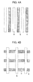
- the direction of the gate trench 8 when viewed from above may be optional, for example, parallel ( Fig. 4(a) ) or perpendicular ( Fig. 4(b) ) to the pillars.
- the gate trenches are arranged inside the n-type pillar layers such that the gate trenches pass through the n-type pillar layers.
- the shape of the gate trenches is formed inside the n-type pillars along the shape of the n-type pillars that surround the p-type pillars such that the gate trenches pass through the n-type pillars.
- a gate-insulating film 9 and a gate electrode 10 are formed inside the gate trench 8.
- High-concentration n+ source regions 11 are selectively formed on a surface of the p-type base layer 7 so as to be adjacent to the gate trench 8.
- a high-concentration p+ base contact region 12 is selectively formed between the source regions 11.
- a source electrode 13 is connected to parts of the source regions 11 and the base contact region 12 by low-resistance connection and extends upward through an interlayer insulating film 14.
- a drain electrode 15 is connected to the back side of the substrate by low-resistance connection.
- Figs. 2 and 3 are comparative results of the cell pitch dependency of the oxide film characteristics and on-resistance characteristics between the case in which the concentration of impurity in a p-type pillar is uniform and the case in which the impurity concentration is increased in an upper layer.
- the cell pitch is altered by changing the width of the n-type pillar.
- the electric field applied to a gate oxide film in the blocking state in Fig. 2 is greatly reduced by increasing the concentration in an upper portion of the p-type pillar.
Landscapes
- Engineering & Computer Science (AREA)
- Mechanical Engineering (AREA)
- Electrodes Of Semiconductors (AREA)
Abstract
Description
- The present invention relates to a silicon carbide semiconductor device in which low on-resistance and high voltage resistance of a semiconductor switching device for power conversion are achieved by using a silicon carbide substrate.
- As a semiconductor switching device for power conversion that uses a silicon carbide substrate, a trench gate type MOSFET has a small unit cell structure and a high current density and is therefore effective in reducing on-resistance.
- In a high-voltage device in which the resistance of a drift layer is predominant, a super junction structure, which forms a repetition of p-type and n-type pillars in the drift layer, is effective in reducing drift layer resistance. These structures can be combined to realize a low-resistance and high-voltage switching device.
- This technique is used in a semiconductor device that includes a substrate formed of a conventional power semiconductor material silicon. For example,
Fig. 2 ofPatent Reference 1 discloses a structure that is provided with a p-type pillar layer between trench gates. - In this structure, an electric field exists not only in the vertical direction from a p-base to a drain but also in the transverse direction from a pillar, and the electric field is not concentrated in a particular portion.
- Thus, high blocking voltage can be maintained even when the concentration of n-type impurity in the n-type pillar layer, which is an electric current path in the on state, is increased.
- However, the dielectric breakdown electric field of silicon carbide is higher by approximately an order of magnitude than that of silicon. Although silicon carbide can maintain a high electric field, the high electric field is also applied to a peripheral insulating oxide film. In a conventional structure, the high electric field is applied to a gate oxide film on the bottom of a trench, and the device may be broken as a result of dielectric breakdown of the insulating oxide film at a low voltage before dielectric breakdown of silicon carbide.
- As a conventional structure for protecting a gate oxide film on the bottom of a trench,
Patent Reference 2 discloses a structure in which a p-base is deepened at a portion apart from the trench. - This allows a depletion layer to be extended from the p-base and a trench gate oxide film to be protected from a high electric field in the blocking state, thereby preventing breakdown of the device due to dielectric breakdown of the oxide film and achieving high voltage resistance.
- In contrast, a super junction structure, which has a p-type pillar in a drift layer, has the same effect in a sense that the depletion layer is expanded in the transverse direction. However, because the depletion layer is expanded on both sides of n-type and p-type pillars, the expansion on the n-type side is insufficient to protect a trench gate oxide film.
- Thus, there is a need for a structure for protecting an oxide film suitable for a super junction structure of a trench gate.
-
Patent Reference 3 discloses a structure that includes a high-concentration p-type region in a junction at a portion connecting a super junction structure and a p-base. This allows a breakdown to occur on the bottom of the high-concentration p-type region, facilitates the flow of an avalanche electric current to a p+ contact, and can improve avalanche capability. - However, the effect of protecting a trench gate oxide film is not clear.
-
- Patent Reference 1: Japanese Unexamined Patent Application Publication No.
2009-43966 - Patent Reference 2: Japanese Unexamined Patent Application Publication No.
2009-260253 - Patent Reference 3: Japanese Unexamined Patent Application Publication No.
2012-39082 - The present invention provides a structure for protecting a gate oxide film from a high electric field in a super junction structure of a trench gate type MOSFET that contains silicon carbide as a substrate material. Measn for solving the Problem
- The present invention provides a semiconductor device that includes a first conductive type drift layer on a silicon carbide substrate, a second conductive type base layer stacked on the first conductive type drift layer, a first conductive type source region formed in a predetermined region on a surface of the base layer, a trench groove that passes through the source region and a base region, a gate electrode formed in at least part of the trench groove with a gate-insulating film interposed therebetween, and a super junction layer that is composed of a second conductive type pillar layer formed in contact with the base layer in the drift layer, wherein the second conductive type pillar layer includes an upper layer and an underlying lower layer, the upper layer being in contact with the base layer, the upper layer has a higher impurity concentration than the lower layer, and an interface between the upper layer and the lower layer of the second conductive type pillar layer and a contact point between the interface and the first conductive type pillar layer are located below the bottom of the trench groove.
- Thus, a contact point between an upper layer of a p-type pillar layer and an n-type pillar has a high concentration. This allows depletion in an n-type pillar layer adjacent to a p-type pillar upper layer portion to occur at a lower voltage than in a lower portion of the p-type pillar layer in the blocking state. Furthermore, because the contact point between the upper layer of the p-type pillar layer and the n-type pillar extends below a trench gate oxide film, the gate oxide film can be surrounded by a depletion layer and can be shielded from a high electric field. This can prevent breakdown of the device resulting from dielectric breakdown of the oxide film, thereby achieving high blocking voltage.
- The present invention also provides the semiconductor device in which the width of an upper layer of the second conductive type pillar is equal to or greater than the width of a lower layer of the second conductive type pillar.
- This allows depletion in the n-type pillar layer adjacent to the p-type pillar upper layer portion to occur at a lower voltage in the blocking state, thereby preventing breakdown of the device due to dielectric breakdown of the oxide film and achieving high blocking voltage.
- There is also provided the semiconductor device in which the second conductive type pillar layer has a stripe shape parallel to the trench groove when viewed from above.
- There is also provided the semiconductor device in which the second conductive type pillar layer has a stripe shape perpendicular to the trench groove when viewed from above.
- Finally, there is provided the semiconductor device in which the second conductive type pillar layer is interspersed as islands when viewed from above, and the trench groove is hexagonal around the pillar layer that serves as the center of the hexagonal when viewed from above.
- In accordance with the present invention, a contact point between an upper layer of a p-type pillar layer and an n-type pillar in a super junction has a high concentration. This allows depletion in an n-type pillar layer adjacent to
a p-type pillar upper layer portion to occur at a lower voltage than in a lower portion of the p-type pillar layer in the blocking state. Because the contact point between the upper layer of the p-type pillar layer and the n-type pillar extends below a trench gate oxide film, the gate oxide film can be surrounded by a depletion layer and can be shielded from a high electric field. This can prevent breakdown of the device resulting from dielectric breakdown of the oxide film, thereby achieving high blocking voltage. -
- [
Fig. 1] Fig. 1 is a cross-sectional view of a striped or island-shaped unit structure (unit cell) of a semiconductor device according to the present invention. - [
Fig. 2] Fig. 2 is a view showing the cell pitch dependency of the electric field characteristics of an oxide film in which the concentration of impurity in a p-type pillar is uniform or is increased in an upper layer. - [
Fig. 3] Fig. 3 is a view showing the cell pitch dependency of the on-resistance characteristics in which the concentration of impurity in a p-type pillar is uniform or is increased in an upper layer. - [
Fig. 4] Fig. 4(a) is a schematic plan view of a striped semiconductor device according to the present invention in which p-type pillars and gate trenches are disposed parallel to each other.Fig. 4(b) is a schematic plan view of a striped semiconductor device according to the present invention in which p-type pillars and gate trenches are disposed perpendicular to each other. - [
Fig. 5] Fig. 5 is a schematic plan view of a semiconductor device according to the present invention in which an island-shaped p-type pillar is surrounded by an n-type pillar. -
Fig. 1 is a cross-sectional view of a striped or island-shaped unit structure (unit cell) of a semiconductor device according to a first embodiment of the present invention. - A
drift layer 2 is disposed on a low-resistance n+ type 4H-SiC substrate 1. - P-
type pillars 4 and n-type pillars 5 are disposed on thedrift layer 2 at regular intervals, thereby constituting asuper junction region 3. - The shape when viewed from above may be a striped shape or a structure in which an island-shaped p-type pillar is surrounded by an n-type pillar, for example, a hexagonal shape.
- An upper portion of the p-type pillar layer is a high-concentration p-
type layer 6 and has a high concentration ratio relative to the n-type pillar. Thus, in the blocking state, depletion in an upper portion of the n-type pillar occurs at a lower voltage than in a lower portion thereof. - A p-
type base layer 7 is stacked on thesuper junction region 3. Agate trench 8 extends from a surface of the p-type base layer 7 to thesuper junction region 3. - In the case of striped pillars as illustrated in
Fig. 4 , the direction of thegate trench 8 when viewed from above may be optional, for example, parallel (Fig. 4(a) ) or perpendicular (Fig. 4(b) ) to the pillars. - In the case where the p-type pillars are parallel to the gate trenches, the gate trenches are arranged inside the n-type pillar layers such that the gate trenches pass through the n-type pillar layers.
- As illustrated in
Fig. 5 , also in the case of island-shaped p-type pillars, the shape of the gate trenches is formed inside the n-type pillars along the shape of the n-type pillars that surround the p-type pillars such that the gate trenches pass through the n-type pillars. - A gate-insulating film 9 and a
gate electrode 10 are formed inside thegate trench 8. High-concentrationn+ source regions 11 are selectively formed on a surface of the p-type base layer 7 so as to be adjacent to thegate trench 8. A high-concentration p+base contact region 12 is selectively formed between thesource regions 11. - A source electrode 13 is connected to parts of the
source regions 11 and thebase contact region 12 by low-resistance connection and extends upward through aninterlayer insulating film 14. - A
drain electrode 15 is connected to the back side of the substrate by low-resistance connection. -
Figs. 2 and 3 are comparative results of the cell pitch dependency of the oxide film characteristics and on-resistance characteristics between the case in which the concentration of impurity in a p-type pillar is uniform and the case in which the impurity concentration is increased in an upper layer. - The cell pitch is altered by changing the width of the n-type pillar.
- The electric field applied to a gate oxide film in the blocking state in
Fig. 2 is greatly reduced by increasing the concentration in an upper portion of the p-type pillar. On the other hand, there is no difference in the on-resistance between the two structures inFig. 3 . This shows that an increase in concentration in the upper portion of the p-type pillar results in suppressed application of an electric field to the oxide film without sacrificing the other characteristics. -
- 1
- n+ type substrate
- 2
- Drift layer
- 3
- Super junction region
- 4
- p-type pillar
- 5
- n-type pillar
- 6
- High-concentration p-type layer
- 7
- p-type base layer
- 8
- Gate trench
- 9
- Gate-insulating film (oxide film)
- 10
- Gate electrode
- 11
- High-concentration n+ source region
- 12
- High-concentration p+ base contact region
- 13
- Source electrode
- 14
- Interlayer insulating film
- 15
- Drain electrode
Claims (5)
- A semiconductor device, comprising:a first conductive type drift layer on a silicon carbide substrate;a second conductive type base layer stacked on the first conductive type drift layer;a first conductive type source region formed in a predetermined region on a surface of the base layer;a trench groove that passes through the source region and a base region;a gate electrode formed in at least part of the trench groove with a gate-insulating film interposed therebetween; anda super junction layer that is composed of a second conductive type pillar layer formed in contact with the base layer in the drift layer,wherein the second conductive type pillar layer includes an upper layer and an underlying lower layer, the upper layer being in contact with the base layer,the upper layer has a higher impurity concentration than the lower layer, andan interface between the upper layer and the lower layer of the second conductive type pillar layer and a contact point between the interface and the first conductive type pillar layer are disposed below the bottom of the trench groove.
- The semiconductor device according to Claim 1, wherein a width of an upper layer of the second conductive type pillar layer is equal to or greater than a width of a lower layer of the second conductive type pillar.
- The semiconductor device according to any one of Claims 1 and 2, wherein the second conductive type pillar layer has a stripe shape parallel to the trench groove when viewed from above.
- The semiconductor device according to any one of Claims 1 and 2, wherein the second conductive type pillar layer has a stripe shape perpendicular to the trench groove when viewed from above.
- The semiconductor device according to any one of Claims 1 and 2, wherein the second conductive type pillar layer is interspersed as islands when viewed from above, and the trench groove is hexagonal around the pillar layer that serves as a center of the hexagonal when viewed from above.
Applications Claiming Priority (2)
| Application Number | Priority Date | Filing Date | Title |
|---|---|---|---|
| JP2012125173 | 2012-05-31 | ||
| PCT/JP2013/061898 WO2013179820A1 (en) | 2012-05-31 | 2013-04-23 | Semiconductor device |
Publications (2)
| Publication Number | Publication Date |
|---|---|
| EP2860761A1 true EP2860761A1 (en) | 2015-04-15 |
| EP2860761A4 EP2860761A4 (en) | 2016-02-24 |
Family
ID=49668760
Family Applications (1)
| Application Number | Title | Priority Date | Filing Date |
|---|---|---|---|
| EP13797744.3A Withdrawn EP2860761A4 (en) | 2012-05-31 | 2013-04-23 | SEMICONDUCTOR DEVICE |
Country Status (4)
| Country | Link |
|---|---|
| US (1) | US20150171169A1 (en) |
| EP (1) | EP2860761A4 (en) |
| JP (1) | JPWO2013179820A1 (en) |
| WO (1) | WO2013179820A1 (en) |
Cited By (2)
| Publication number | Priority date | Publication date | Assignee | Title |
|---|---|---|---|---|
| CN105576022A (en) * | 2014-10-11 | 2016-05-11 | 中航(重庆)微电子有限公司 | Semiconductor device with super-junction structure and preparation method thereof |
| CN110116120A (en) * | 2019-04-23 | 2019-08-13 | 佛山市妇幼保健院 | A kind of cleaning sterilizing device of rubber bulb |
Families Citing this family (4)
| Publication number | Priority date | Publication date | Assignee | Title |
|---|---|---|---|---|
| JPWO2020129175A1 (en) * | 2018-12-19 | 2021-11-04 | サンケン電気株式会社 | Semiconductor device |
| JP7543950B2 (en) | 2021-03-08 | 2024-09-03 | 富士電機株式会社 | Method for manufacturing super-junction silicon carbide semiconductor device |
| JP7748318B2 (en) | 2022-03-24 | 2025-10-02 | 株式会社東芝 | Silicon carbide semiconductor device |
| JP7702923B2 (en) * | 2022-08-09 | 2025-07-04 | 三菱電機株式会社 | Method for manufacturing silicon carbide semiconductor device |
Family Cites Families (14)
| Publication number | Priority date | Publication date | Assignee | Title |
|---|---|---|---|---|
| JPH10229190A (en) * | 1997-02-14 | 1998-08-25 | Denso Corp | Silicon carbide semiconductor device and method of manufacturing the same |
| JP3913564B2 (en) * | 2002-01-31 | 2007-05-09 | 富士電機ホールディングス株式会社 | Superjunction semiconductor device manufacturing method |
| JP4536366B2 (en) * | 2003-12-22 | 2010-09-01 | 株式会社豊田中央研究所 | Semiconductor device and its design support program |
| JP4813762B2 (en) * | 2003-12-25 | 2011-11-09 | ルネサスエレクトロニクス株式会社 | Semiconductor device and manufacturing method thereof |
| JP5132123B2 (en) * | 2006-11-01 | 2013-01-30 | 株式会社東芝 | Power semiconductor device |
| JP2008300420A (en) * | 2007-05-29 | 2008-12-11 | Nec Electronics Corp | Semiconductor device and manufacturing method of semiconductor device |
| JP2009043966A (en) | 2007-08-09 | 2009-02-26 | Toshiba Corp | Semiconductor device and manufacturing method thereof |
| US20090057713A1 (en) * | 2007-08-31 | 2009-03-05 | Infineon Technologies Austria Ag | Semiconductor device with a semiconductor body |
| JP5721308B2 (en) | 2008-03-26 | 2015-05-20 | ローム株式会社 | Semiconductor device |
| JP2009302436A (en) * | 2008-06-17 | 2009-12-24 | Denso Corp | Method of manufacturing silicon carbide semiconductor device |
| JP2011044513A (en) * | 2009-08-20 | 2011-03-03 | National Institute Of Advanced Industrial Science & Technology | Silicon carbide semiconductor device |
| JP5136674B2 (en) * | 2010-07-12 | 2013-02-06 | 株式会社デンソー | Semiconductor device and manufacturing method thereof |
| JP5740108B2 (en) * | 2010-07-16 | 2015-06-24 | 株式会社東芝 | Semiconductor device |
| JP2012164707A (en) * | 2011-02-03 | 2012-08-30 | Panasonic Corp | Semiconductor device, and method of manufacturing the same |
-
2013
- 2013-04-23 US US14/404,490 patent/US20150171169A1/en not_active Abandoned
- 2013-04-23 JP JP2014518346A patent/JPWO2013179820A1/en active Pending
- 2013-04-23 EP EP13797744.3A patent/EP2860761A4/en not_active Withdrawn
- 2013-04-23 WO PCT/JP2013/061898 patent/WO2013179820A1/en not_active Ceased
Cited By (4)
| Publication number | Priority date | Publication date | Assignee | Title |
|---|---|---|---|---|
| CN105576022A (en) * | 2014-10-11 | 2016-05-11 | 中航(重庆)微电子有限公司 | Semiconductor device with super-junction structure and preparation method thereof |
| CN105576022B (en) * | 2014-10-11 | 2019-02-22 | 华润微电子(重庆)有限公司 | Semiconductor device with superjunction structure and preparation method thereof |
| CN110116120A (en) * | 2019-04-23 | 2019-08-13 | 佛山市妇幼保健院 | A kind of cleaning sterilizing device of rubber bulb |
| CN110116120B (en) * | 2019-04-23 | 2024-01-09 | 佛山市妇幼保健院 | A cleaning and disinfection device for rubber suction balls |
Also Published As
| Publication number | Publication date |
|---|---|
| WO2013179820A1 (en) | 2013-12-05 |
| JPWO2013179820A1 (en) | 2016-01-18 |
| EP2860761A4 (en) | 2016-02-24 |
| US20150171169A1 (en) | 2015-06-18 |
Similar Documents
| Publication | Publication Date | Title |
|---|---|---|
| US8957502B2 (en) | Semiconductor device | |
| US9059238B2 (en) | Semiconductor device | |
| US7973363B2 (en) | IGBT semiconductor device | |
| US9577087B2 (en) | Semiconductor apparatus | |
| JP5701802B2 (en) | Power semiconductor device | |
| US7655975B2 (en) | Power trench transistor | |
| US8232593B2 (en) | Power semiconductor device | |
| US8742500B2 (en) | Semiconductor device | |
| US10276654B2 (en) | Semiconductor device with parallel PN structures | |
| US8860171B2 (en) | Semiconductor device having diode characteristic | |
| US8217454B2 (en) | Semiconductor device | |
| US11088276B2 (en) | Silicon carbide semiconductor device | |
| EP2667418B1 (en) | Semiconductor device | |
| JP2001135819A (en) | Super junction semiconductor device | |
| US20150171169A1 (en) | Semiconductor device | |
| JP2014135367A (en) | Semiconductor device | |
| US12205984B2 (en) | Semiconductor device with surface and deep guard rings | |
| JP5694285B2 (en) | Semiconductor device | |
| JPWO2013080641A1 (en) | Semiconductor device | |
| US9082842B2 (en) | Semiconductor device | |
| JP2008277353A (en) | Semiconductor device | |
| US9356100B2 (en) | Semiconductor device | |
| JP2007317683A (en) | Semiconductor device | |
| JP2009111237A (en) | Semiconductor element | |
| KR102598676B1 (en) | Pillar strucutre and super junction semiconductor device including the same |
Legal Events
| Date | Code | Title | Description |
|---|---|---|---|
| PUAI | Public reference made under article 153(3) epc to a published international application that has entered the european phase |
Free format text: ORIGINAL CODE: 0009012 |
|
| 17P | Request for examination filed |
Effective date: 20141223 |
|
| AK | Designated contracting states |
Kind code of ref document: A1 Designated state(s): AL AT BE BG CH CY CZ DE DK EE ES FI FR GB GR HR HU IE IS IT LI LT LU LV MC MK MT NL NO PL PT RO RS SE SI SK SM TR |
|
| AX | Request for extension of the european patent |
Extension state: BA ME |
|
| DAX | Request for extension of the european patent (deleted) | ||
| RA4 | Supplementary search report drawn up and despatched (corrected) |
Effective date: 20160121 |
|
| RIC1 | Information provided on ipc code assigned before grant |
Ipc: H01L 29/12 20060101ALI20160115BHEP Ipc: H01L 29/06 20060101ALI20160115BHEP Ipc: H01L 29/78 20060101AFI20160115BHEP |
|
| STAA | Information on the status of an ep patent application or granted ep patent |
Free format text: STATUS: THE APPLICATION IS DEEMED TO BE WITHDRAWN |
|
| 18D | Application deemed to be withdrawn |
Effective date: 20160820 |