EP2850917B1 - Lichtquellenschaltkreis - Google Patents
Lichtquellenschaltkreis Download PDFInfo
- Publication number
- EP2850917B1 EP2850917B1 EP13729464.1A EP13729464A EP2850917B1 EP 2850917 B1 EP2850917 B1 EP 2850917B1 EP 13729464 A EP13729464 A EP 13729464A EP 2850917 B1 EP2850917 B1 EP 2850917B1
- Authority
- EP
- European Patent Office
- Prior art keywords
- light source
- group
- emitting diodes
- light emitting
- source circuitry
- Prior art date
- Legal status (The legal status is an assumption and is not a legal conclusion. Google has not performed a legal analysis and makes no representation as to the accuracy of the status listed.)
- Active
Links
- 230000007423 decrease Effects 0.000 claims description 5
- 238000004519 manufacturing process Methods 0.000 claims description 3
- 239000004571 lime Substances 0.000 description 10
- 235000008733 Citrus aurantifolia Nutrition 0.000 description 9
- 235000011941 Tilia x europaea Nutrition 0.000 description 9
- 239000003086 colorant Substances 0.000 description 6
- 230000005669 field effect Effects 0.000 description 4
- 230000004907 flux Effects 0.000 description 3
- 230000008901 benefit Effects 0.000 description 2
- 230000008859 change Effects 0.000 description 2
- 230000001419 dependent effect Effects 0.000 description 2
- 235000019648 warmth Nutrition 0.000 description 2
- 206010016334 Feeling hot Diseases 0.000 description 1
- 230000002411 adverse Effects 0.000 description 1
- 238000005516 engineering process Methods 0.000 description 1
- 230000006870 function Effects 0.000 description 1
- 238000005286 illumination Methods 0.000 description 1
- 239000000203 mixture Substances 0.000 description 1
- 230000004048 modification Effects 0.000 description 1
- 238000012986 modification Methods 0.000 description 1
- 230000036651 mood Effects 0.000 description 1
- 230000008447 perception Effects 0.000 description 1
- 230000001105 regulatory effect Effects 0.000 description 1
- 230000035945 sensitivity Effects 0.000 description 1
Images

Classifications
-
- H—ELECTRICITY
- H05—ELECTRIC TECHNIQUES NOT OTHERWISE PROVIDED FOR
- H05B—ELECTRIC HEATING; ELECTRIC LIGHT SOURCES NOT OTHERWISE PROVIDED FOR; CIRCUIT ARRANGEMENTS FOR ELECTRIC LIGHT SOURCES, IN GENERAL
- H05B45/00—Circuit arrangements for operating light-emitting diodes [LED]
- H05B45/30—Driver circuits
- H05B45/395—Linear regulators
-
- H—ELECTRICITY
- H05—ELECTRIC TECHNIQUES NOT OTHERWISE PROVIDED FOR
- H05B—ELECTRIC HEATING; ELECTRIC LIGHT SOURCES NOT OTHERWISE PROVIDED FOR; CIRCUIT ARRANGEMENTS FOR ELECTRIC LIGHT SOURCES, IN GENERAL
- H05B45/00—Circuit arrangements for operating light-emitting diodes [LED]
- H05B45/20—Controlling the colour of the light
-
- H—ELECTRICITY
- H05—ELECTRIC TECHNIQUES NOT OTHERWISE PROVIDED FOR
- H05B—ELECTRIC HEATING; ELECTRIC LIGHT SOURCES NOT OTHERWISE PROVIDED FOR; CIRCUIT ARRANGEMENTS FOR ELECTRIC LIGHT SOURCES, IN GENERAL
- H05B45/00—Circuit arrangements for operating light-emitting diodes [LED]
- H05B45/40—Details of LED load circuits
- H05B45/44—Details of LED load circuits with an active control inside an LED matrix
- H05B45/46—Details of LED load circuits with an active control inside an LED matrix having LEDs disposed in parallel lines
-
- H—ELECTRICITY
- H05—ELECTRIC TECHNIQUES NOT OTHERWISE PROVIDED FOR
- H05B—ELECTRIC HEATING; ELECTRIC LIGHT SOURCES NOT OTHERWISE PROVIDED FOR; CIRCUIT ARRANGEMENTS FOR ELECTRIC LIGHT SOURCES, IN GENERAL
- H05B47/00—Circuit arrangements for operating light sources in general, i.e. where the type of light source is not relevant
- H05B47/20—Responsive to malfunctions or to light source life; for protection
- H05B47/25—Circuit arrangements for protecting against overcurrent
-
- Y—GENERAL TAGGING OF NEW TECHNOLOGICAL DEVELOPMENTS; GENERAL TAGGING OF CROSS-SECTIONAL TECHNOLOGIES SPANNING OVER SEVERAL SECTIONS OF THE IPC; TECHNICAL SUBJECTS COVERED BY FORMER USPC CROSS-REFERENCE ART COLLECTIONS [XRACs] AND DIGESTS
- Y02—TECHNOLOGIES OR APPLICATIONS FOR MITIGATION OR ADAPTATION AGAINST CLIMATE CHANGE
- Y02B—CLIMATE CHANGE MITIGATION TECHNOLOGIES RELATED TO BUILDINGS, e.g. HOUSING, HOUSE APPLIANCES OR RELATED END-USER APPLICATIONS
- Y02B20/00—Energy efficient lighting technologies, e.g. halogen lamps or gas discharge lamps
- Y02B20/30—Semiconductor lamps, e.g. solid state lamps [SSL] light emitting diodes [LED] or organic LED [OLED]
Definitions
- the invention relates to light source circuitry and particularly to light source circuitry comprising light emitting diodes.
- LEDs light emitting diodes
- LEDs Due to their high luminous efficacy, light emitting diodes (LEDs) are being used in an ever-increasing range of lighting applications. LEDs provide a great number of different functionalities that are not possible, or are not as easy to achieve, with conventional light bulbs.
- One such functionality is the ability to change the tint or color of a single light bulb.
- this functionality is achieved by supplying the LED bulb with LEDs of a plurality of different colors, and by using pulse width modulation (PWM) to control the amount of current that is supplied to the LED's of each color.
- PWM pulse width modulation
- the use of PWM requires a power supply and circuitry that is able to cope with changing power levels and with high frequencies.
- WO2010/122463 A1 discloses an illumination device with three strings of LEDs. There is, therefore, a need for an LED bulb having a changeable color or tint, but which does not use PWM to provide this functionality.
- the present invention provides light source circuitry comprising a first group of one or more light emitting diodes operable to emit light of a first color, a second group of one or more light emitting diodes operable to emit light of a second color, and a third group of one or more light emitting diodes operable to emit light of a third color.
- the first, second and third groups of light emitting diodes are arranged such that, when a fixed current arrives at the light source circuitry, the fixed current is shared between the first, second and third groups.
- the circuitry is configured such that a proportion of the fixed current that flows through each of the first and second groups is controllable in dependence on a received control signal and such that the remainder of the fixed current flows through the third group.
- the combined emissions of the light source circuitry can be gradually varied over a range of chromaticities, using only a single control signal.
- changing the chromaticity of the combined emission is relatively straightforward and can be carried out using existing infrastructure, such as conventional dimmer switches regulating a mains power supply.
- changing the chromaticity does not require the use of PWM and so the PWM-specific requirements on the power are not necessary. Consequently, the power supply to the circuitry can be simpler.
- Many existing power supplies for conventional LED bulbs are configured so as to provide a constant current. As such, the light source circuitry according to the invention can be easily utilized with existing power supplies.
- the light source circuitry may further comprise a first transistor connected in series with the first group of light emitting diodes, a second transistor connected in series with the second group of light emitting diodes, wherein the circuitry is configured such that a variation in the control signal causes a variation in the proportion of the fixed current that flows through the first transistor and second transistor.
- the circuitry may be configured such that a first signal based on the control signal is provided to the control terminal of the first transistor and such that a second signal based on the control signal is provided to the control terminal of the second transistor.
- the light source circuitry may be configured such that the first and second signals based on the control signal vary relative to one another in dependence on the control signal.
- the light source circuitry may further comprise a third transistor connected in series with the third group of light emitting diodes. A third signal based on the control signal may be received at the control terminal of the third transistor, wherein the third signal is always larger than the first and second signals.
- the combined forward voltage of the third group of light emitting diodes may be larger than the combined forward voltage of the first group of light emitting diodes and the combined forward voltage of the second group of light emitting diodes.
- the light source circuitry may be configured such that when the control signal is at a first level, the largest proportion of the fixed current flows through the third group of light emitting diodes and such that, as the control signal changes to second level, the proportions of the fixed current that flow through the first and second groups of light emitting diodes increase.
- the circuitry may be configured such that, as the control signal changes from the second level to a third level, the proportion of the fixed current that flows in the first group of light emitting diodes decreases, and the proportion of the fixed current that flows in the second group of light emitting diodes continues to increase.
- the second group of light emitting diodes may be constituted by one or more light emitting diodes operable to emit red-colored light
- the third group of light emitting diodes may be constituted by one or more light emitting diodes operable to emit white-colored light
- the first group of light emitting diodes may be constituted by one or more light emitting diodes the combined emission of which is lime-colored.
- the light source circuitry may be configured such that, as the control signal gradually changes from a first level to a different level, the color of the combined emissions of the first, second and third groups of light emitting diodes changes generally in accordance with the Planckian locus.
- the Planckian locus is the representation of different tints of white that are available using various different technologies. Colors falling on the Planckian locus are perceived by consumers to be white, but having different "warmths".
- the light source circuitry can be used to provide subtle changes in atmosphere by varying the warmth of the emitted light. Changing the color of light along the Planckian locus can influence people's moods and their perception of the ambient atmosphere. In contrast, when deviating from the Planckian locus, people may perceive the light to be colored instead of white, and so the above advantages may not apply.
- the present invention provides a method of manufacturing light source circuitry comprising providing a first group of one or more light emitting diodes operable to emit light of a first color, providing a second group of one or more light emitting diodes operable to emit light of a second color, providing a third group of one or more light emitting diodes operable to emit light of third color, arranging the first, second and third groups of light emitting diodes such that, when a fixed current arrives at the light source circuitry, the fixed current is shared between the first, second and third groups, and configuring the light source such that a proportion of the fixed current that flows through each of the first and second groups is controllable in dependence on a received control signal and such that the remainder of the fixed current flows through the third group.
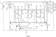
- Figure 1 is an example of light source circuitry 1 in accordance with the present invention.
- the light source circuitry 1 comprises plural groups of LEDs 10, 12, 14.
- the light source circuitry 1 of Figure 1 comprises a first group of LEDs 10, a second group of LEDs 12 and a third group of LEDs 14.
- Each of the first, second and third groups of LEDs 10, 12, 14 comprises one or more LEDs e.g. 10A, 12A, 14A.
- Each of the groups of LEDs 10, 12, 14 is operable to emit light of a different color.
- the first group of LEDs 10 consists of plural LEDs 10A, 10B, in this instance two, which are operable to emit lime-colored light (hereafter referred to as lime LEDs).
- the second group of LEDs 12 consists of plural LEDs 12A, 12B 12C, in this example three, which are operable to emit red-colored light (hereafter referred to as red LEDs).
- the third group of LEDs 14 consists of plural LEDs 14A, 14B, 14C, in this instance three, which are operable to emit white-colored light (hereafter white LEDs).
- the LEDs within each of the first, second and third groups 10, 12, 14 are connected in series with one another.
- the plural groups of LEDs 10, 12, 14 are connected in parallel with one another. As such, a fixed current arriving at the circuitry is shared among the plural groups of LEDs 10, 12, 14.
- the light source circuitry 1 also comprises a current source 70 which provides the fixed current.
- the light source circuitry 1 is configured such that a proportion of the fixed current that is provided to each of the first and second groups 10, 12 is controllable in dependence on a received control signal.
- the circuitry is also configured such that the remainder of the fixed current is provided to the third group 14.
- the light source circuitry 10 is configured such that when the control signal is at a first level, the majority of the fixed current flows through the white LEDs of the third group 14. As the control signal gradually moves towards a second level, the currents flowing through the lime and red LEDs of the first and second groups 10, 12 respectively both increase. Between the first and second levels, the current flowing through the lime LEDs 10A, 10B is larger than the current flowing through the red LEDs 12A, 12B, 12C. As the control signal gradually moves beyond the second level to a third level, the current in the lime LEDs 10A, 10B begins gradually to decrease, while the current in the red LEDs 12A, 12B, 12C continues to increase.
- the current flowing in the white LEDs 14A, 14B, 14C gradually decreases as the control signal moves from the first to third levels.
- the current in the white LEDs 14A, 14B, 14C is nearly zero at the third level.
- the current flowing in the second group 12 becomes larger than the current flowing in the first group 10.
- the light source circuitry 1 being configured in this way allows the chromaticity of the combined emissions of the first, second and third groups of LEDs 10, 12, 14 substantially to follow the Planckian locus (also known as the black body locus) as the control signal changes from the first to third levels.
- the first group of LEDs 10 is connected in series with a first transistor 16.
- the second group of LEDs 12 is connected in series with a second transistor 18.
- the first and second transistors 16, 18 are n-channel bipolar junction transistors (BJTs).
- the base terminals of the first and second transistors 16, 18 are connected to one another via a first resistor 20.
- a first conductive path 19 connects the base terminal of the first transistor 16 and the first resistor 20.
- a second conductive path 21 connects the base terminal of the second transistor 16 and the first resistor 20.
- the presence of the first resistor 20 creates a dependency, so that the currents in the first and second groups of LEDs 10, 12 do not differ from one another by too much. This is achieved because the first resistor 20 limits the difference that can exist between the voltages at the base terminals of the first and second transistors 16, 18.
- the first resistor 20 may be omitted from the circuitry 1.
- the light source circuitry 1 comprises a controllable voltage supply 22. This provides a voltage which acts as the control signal for varying the current that flows through the first and second groups of LEDs 10, 12.
- the controllable voltage supply 22 is connected to the base terminal of at least the second transistor 18 so as to vary the amount of current that flows through the second transistor 18, and thus also through the second group of LEDs 12.
- the controllable voltage supply is also connected to the base terminal of the first transistor 16 so as to vary the amount of current that flows through the first transistor 16, and thus also through the first group of LEDs 10.
- the first group of LEDs 10 is connected to the collector terminal of the first transistor 16.
- the emitter terminal of the first transistor 16 is connected to ground, via a second resistor 64.
- the second group of LEDs 12 is connected to the collector terminal of the second transistor 18.
- the emitter terminal of the second transistor 18 is connected to ground, via a third resistor 68.
- the resistances of the second and third resistors 64, 68 are the same.
- the presence of the second and third resistors 64, 68 makes the circuit more stable over a range of different temperatures and between different instances of the light source circuitry 1. This is because their presence reduces the sensitivity to base-emitter voltage drift.
- the third group of LEDs 14 is connected to ground. Whereas the current flowing through the first and second groups of LEDs 10, 12 is dependent on the control signal, the current through the third group of LEDs 14 is not directly controllable, but instead comprises the remainder of the first current that does not flow through the first and second groups 10, 12..
- the controllable voltage supply 22 is connected to the base terminal of the second transistor 18 via first control circuitry 24A.
- the controllable voltage supply 22 is connected to the base terminal of the first transistor 16 via second control circuitry 24B.
- the first and second control circuitries 24A, 24B are configured so as to ensure that the combined light emissions of the first, second and third groups of LEDs 10, 12, 14 follows the Planckian locus as closely as possible for as long as possible. In the example of Figure 1 , this is achieved using analogue components, including diodes, resistors and transistors. However, it will be appreciated that it may instead be achieved using a micro-processor configured to receive a single voltage and to use this voltage to supply a suitable current to the base terminal of at least one of the first and second transistors 16, 18. Alternatively, this may be achieved using operational amplifiers.
- the first control circuitry 24A comprises one or more, in this instance three, parallel circuit branches 26A, 26B, 26C connected between the controllable voltage supply 22 and the second conductive path 21.
- a first branch 26A comprises a fourth resistor 28.
- a second branch 26B comprises a fifth resistor 30 in series with a reverse-biased first Zener diode 32.
- a third branch 26C comprises a sixth resistor 34 in series with a reverse-biased second Zener diode 36.
- the presence of the first and second Zener diodes 32, 36 means that a significant current flows through the second and third branches 26B, 26C only when the potential difference between the controllable voltage supply 22 and the second conductive path 21 exceeds a predetermined value (i.e.
- the reverse voltage of the Zener diodes 32, 36 current always flows through the first branch 26A as long as a potential difference exists.
- the first branch 26A is connected to the second conductive path 21 at a location nearest to the base terminal of the second transistor 18.
- the third branch 26C is connected to the second conductive path 21 at a location nearest to the first resistor 20.
- the second branch 26B is connected to the second conductive path 21 at a location between the locations at which the first and third branches 26A, 26C are connected to the second conductive path 21.
- the second control circuitry 24B comprises one or more branches 38A, 38B, 38C, in this instance three, connected in parallel between the controllable voltage supply 22 and the first conductive path 19.
- a first branch 38A comprises a seventh resistor 40.
- a second branch 38B comprises a forward biased conventional diode 42 connected in series with an eighth resistor 44.
- a third branch 38C comprises a ninth resistor 46 in series with a third reverse-biased Zener diode 48.
- the presence of the first conventional diode in the second branch 38B means that a significant current will only flow in the second branch when the potential difference between the controllable voltage supply and the first conductive path 19 is above the forward voltage of the diode 42.
- the presence of the third Zener diode 48 means that a significant current will only flow in the third branch 38C when the potential difference is greater than the reverse voltage of the third Zener diode 48. A current will always flow in the first branch 38A as long as a potential difference exists.
- the second branch 38B is connected to the first conductive path 19 at a location nearest to the base terminal of the first transistor 16.
- the third branch 38C is connected to the first conductive path 19 at a location nearest to the first resistor 20.
- the first branch 38A is connected to the first conductive path 19 at a location between the locations at which the second and third branches 38B, 38C are connected to the first conductive path 19.
- the second control circuitry 24B also comprises first and second control transistors 50, 52.
- the first and second control transistors 50, 52 comprise p-channel BJTs.
- the controllable voltage supply 22 is connected to the base terminal of the first control transistor 50 via a tenth resistor 54 connected in series with a fourth Zener diode 56.
- the controllable voltage supply 22 is connected to the base terminal of the second control transistor 52 via an eleventh resistor 58 connected in series with a fifth Zener diode 60.
- the collector of the first control transistor 50 is connected to the first conductive path 19, in this example at a location between the locations at which the first and third branches 38A, 38C of the second control circuitry 24B connect to the first conductive path 19.
- the emitter of the first control transistor 50 is connected to ground.
- the collector of the second control transistor 52 is connected to the base terminal of the first transistor 16, in this example at a location between the locations at which the first and second branches 38A, 38B of the second control circuitry 24B connect to the first conductive path 19.
- the emitter of the second control transistor 50 is connected to ground.
- the resistances of the tenth and eleventh resistors 45, 58 may be the same.
- first and second control transistors 50, 52 means that, when a potential difference between the base terminals of the first and second control transistors 50, 52 and the controllable voltage supply 22 is in excess of the reverse voltages of the fourth and fifth Zener diodes 56, 60, some current will flow through first and second control transistors from the first conductive path. As such, less current flows to the base terminal of the first transistor 16, and so less current flows through the collector-emitter junction of the first transistor 16 which means less current also flows through the first group of LEDs 10, thus reducing the intensity of the light emitted by the first group of LEDs 10.
- Each of the first to fifth Zener diodes 32, 36, 48, 56, 60 may have a different reverse voltage.
- the reverse voltages of the Zener diodes 32, 36, 48, 56, 60 are selected based on the range of voltages of the control supply.
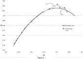
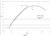
- Each of the Zener diodes is responsible for a change in the gradient of the chromaticity graph (see Figure 2 ) of the light source circuitry 1. As such, the inclusion of the Zener diodes 32, 36, 48, 56, 60 allows the light source circuitry to track the Planckian Locus over a wider range of chromaticities. This will be apparent from a comparison of Figures 2 and 4 .
- the light source circuitry 1 may also comprise a current protection branch connected between the current source 70 and ground.
- a current protection branch may be connected in parallel with the first, second and third groups of LEDs 10, 12, 14.
- the current protection branch may comprise at least a resistor connected in series with a reverse-biased Zener diode. When, the potential difference between the current source 70 and ground exceeds the reverse voltage of the Zener diode, the current protection branch begins to conduct current. This reduces the amount of current that can flow through the first, second and third groups of LEDs 10, 12, 14 thereby protecting the LEDs against damage due to excessive currents.
- the electrical components shown in Figure 1 have the following electrical characteristics. It will be appreciated, however, that the below characteristics are examples only, and that components having different characteristics may instead be used:
- Table 1 shows the currents flowing through the lime, red and white LEDs in light source circuitry 1 having the above characteristics for a varying control signal: Table 1 Control Signal (V) I LIME (A) I RED (A) I WHITE (A) 1.0 0.012 0.015 0.673 1.5 0.036 0.03 0.634 2.0 0.056 0.04 0.604 2.5 0.086 0.055 0.559 3.0 0.125 0.075 0.5 3.5 0.173 0.1 0.427 4.0 0.221 0.13 0.349 4.5 0.252 0.165 0.283 5.0 0.293 0.21 0.197 5.5 0.318 0.255 0.127 6.0 0.323 0.305 0.072 6.5 0.326 0.35 0.024 7.0 0.298 0.38 0.022 7.5 0.28 0.41 0.01 8.0 0.25 0.44 0.01
- the first control signal level is between 1.0 and 1.5V.
- the second control signal level, at which the current flowing through the lime LEDs 10A, 10B, 10C, begins to drop is located between 6.5V and 7.0V.
- Table 2 shows the chromaticity and the flux levels of the combined emissions of the first, second and third groups of LEDs 10, 12, 14 as the control signal changes gradually from a first level to the third level.
- Table 2 Control Signal (V) C x C y Flux (Lumen) 1.0 0.333774 0.343104 450.8929274 1.5 0.341650 0.349198 465.1289412 2.0 0.346767 0.353348 472.9506647 2.5 0.353973 0.358896 481.0644331 3.0 0.363155 0.365567 487.3098279 3.5 0.374633 0.373591 490.2112517 4.0 0.388160 0.381987 487.529364 4.5 0.402408 0.388265 478.5973982 5.0 0.423588 0.398195 462.2534738 5.5 0.446396 0.407129 440.775934 6.0 0.472420 0.413898 413.0114279 6.5 0.503973 0.422884 379.8113722 7.0 0.5136
- light source circuitry in accordance with the present invention allows the tint or color of light produced by the light source circuitry to be varied without the need to use PWM. In addition, it requires only a variation in a single control signal to obtain a wide range of different tints or colors, which in some embodiments follow closely the Planckian locus.
- the structural simplicity of the light source circuitry, and the fact that it needs only a single control signal to vary the tint across a wide range of chromaticities, means that the cost of manufacture of the light source circuitry and any appliance, such as a bulb, which includes the light source circuitry can remain relatively low.
- Figure 3 shows an uncompensated version 3 of the light source circuitry of Figure 1 .
- the uncompensated light source circuitry 3 is substantially the same as the circuitry 1 of Figure 1 except that it includes much simplified control circuitries 24A, 24B.
- the first control circuitry 24A is constituted by a resistor 27 connected between the controllable voltage supply 22 and the second conductive path 21.
- the second control circuitry 24B is constituted by a resistor 39 connected between the controllable voltage supply 22 and the first conductive path 21.
- Figure 4 shows a graph of the chromaticity of the combined emissions of light source circuitry 3 of Figure 3 (denoted G2) relative to the Planckian Locus (denoted PL). As can be seen, the combined emissions still track the Planckian Locus, but over a shorter range of chromaticities.
- the electrical characteristics of the components of the light source circuitry 3 were the same as the characteristics of the corresponding components listed above with reference to Figure 1 (i.e. the resistances of the resistors 20, 64 and 68 were the same, as well as the forward voltages of the LEDs 10, 12, 14, and the voltage and current of the controllable voltage and current sources 22, 70 respectively).
- the resistance of the resistor 27 of the first control circuitry 24A was 4,200 ⁇ .
- the resistance of the resistor 39 of the second control circuitry 24B was 2,400 ⁇ .
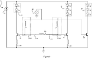
- Figure 5 is an example of another alternative arrangement of light source circuitry 150 in accordance with the invention.
- the light source circuitry 5 of Figure 5 is substantially the same as the uncompensated light source circuitry of Figure 3 .
- the light source circuitry 5 of Figure 5 also comprises a third transistor 500 connected in series with the third group of LEDs 14.
- the third group of LEDs are connected to the collector terminal of the third transistor 500.
- the emitter terminal of the third transistor 500 is connected to ground.
- the controllable voltage supply 22 is connected to the base terminal of the third transistor 500.
- the connection between the controllable voltage supply 22 and the base terminal of the third transistor 500 may include no resistor, or may include a resistor that is of significantly lower resistance than the resistors 27, 39 of the first and second control circuitries 24A, 24B.
- the light source circuitry 5 of Figure 5 is configured such that when the control signal is at a first level, the majority of the current flows through the white LEDs of the third group 14. As the control signal gradually moves towards a second level, the currents flowing through the lime and red LEDs of the first second groups 10, 12 respectively both increase. The current flowing through the LEDs in the first group 10 is larger than the current flowing through the LEDs of the second group 12. In this example, the current flowing through the second group of LEDs 12 never becomes larger than the current flowing through first group of LEDs 10. As such, the combined emission of the light source circuitry 5 follows the Planckian locus over a shorter range of chromaticities than does the example of Figure 1 .
- the current flowing in the third group 14 (i.e. the remainder of the current that is not flowing in the first and second groups 10, 12) gradually decreases as the control signal moves from the first to third levels.
- the light source circuitry 5 of Figure 5 operates in this way at least in part because the combined forward voltage of the third group of LEDs 14 is greater than the forward voltages of the first and second groups of LEDs 10, 12.
- the forward voltage of the second group of LEDs 12 is preferably similar to the forward voltage of the first group of LEDs 10.
- the characteristics of the components of the circuitry 5 of Figure 5 are substantially the same as those in Figure 3 , except that the resistance of the resistor 27 of the first control circuitry 24A is 2,400 ⁇ and the resistance of the resistor 39 of the second control circuitry 24B is 3000 ⁇
- Figures 1 , 3 and 5 show the fixed current source 70 as part of the light source circuitry 1, 3, 5, it will be appreciated that this may be separable. As such, the circuitry 1, 3, 5 may instead be configured to be connectable to (and so not actually including) the fixed current source 70.
- the fixed current source 70 may comprise, for example, a mains-power flyback converter. Alternatively, the fixed current source 70 may comprise any other means for providing a fixed current to the light source circuitry 1, 3, 5.
- controllable voltage source 22 for providing the control signal may be separate or separable from the light source circuitry 1, 3, 5.
- the controllable voltage source 22 may comprise, for example, a rectified mains signal with, for example, an output voltage between 1V and 10V.
- Figures 1 , 3 and 5 show the groups of LEDs 10, 12, 14 connected to the collector terminals of the various transistors 16, 18, 500, it will be understood that the groups of LEDs may instead be connected to the emitter terminals.
- the specific examples include n-channel BJTs, in some examples p-channel BJTs may be used.
- field effect transistors may be used. In examples which include field-effect transistors, where a connection is described above as being to the base terminal, the connection is instead to the gate terminal. Similarly, where a connection is described as being with the emitter terminal or collector terminal, in examples including field-effect transistors the connection is instead to the drain or source terminals respectively.
- the gate terminal and the base terminal of field-effect transistors and BJTs respectively may be collectively referred to herein as control terminals. This is because a signal provided to those terminals controls the current that flows through the transistor.
- each of the groups of LEDs 10, 12, 14 may include LEDs of different colors, the combined emissions of which result in light of a desired color.
- the first group of LEDs 14, instead of all being Lime LEDs, may be comprised of a mixture of green LEDs and amber LEDs to produce a lime-colored combined emission.
- the colors and quantities of LEDs are selected so as to be able to produce a combined emission that closely follows the Planckian locus.
- different colored LEDs to those described above may be used.
- different numbers of LEDs to those described above may be used.
- the Figures show the LEDs of each group connected in series, in some alternatives the LEDs of each group may be connected in parallel, or in a combination of in series an in parallel.
- the light source circuitry according to the present invention may be used to create LED light sources such as retrofit lamps, LED luminairs, or lamp for professional applications such as lamps used in theaters or lamps for illuminating steps.
Landscapes
- Circuit Arrangement For Electric Light Sources In General (AREA)
Claims (13)
- Lichtquellenschaltkreis, umfassend:eine erste Gruppe von einer oder mehreren Licht emittierenden Dioden, die betriebsfähig sind, um Licht einer ersten Farbe zu emittieren;eine zweite Gruppe von einer oder mehreren Licht emittierenden Dioden, die betriebsfähig sind, um Licht einer zweiten Farbe zu emittieren; undeine dritte Gruppe von einer oder mehreren Licht emittierenden Dioden, die betriebsfähig sind, um Licht einer dritten Farbe zu emittieren,wobei die erste, zweite und dritte Gruppe von Licht emittierenden Dioden so angeordnet sind, dass, wenn ein festgelegter Strom an dem Lichtquellenschaltkreis ankommt, der festgelegte Strom auf die erste, zweite und dritte Gruppe aufgeteilt wird, unddadurch gekennzeichnet ist, dassder Lichtquellenschaltkreis so ausgelegt ist, dass ein Anteil des festgelegten Stroms, der durch jede der ersten und zweiten Gruppe fließt, in Abhängigkeit von einem einzelnen empfangenen Steuersignal steuerbar ist, und so, dass der Rest des festgelegten Stroms durch die dritte Gruppe fließt.
- Lichtquellenschaltkreis nach Anspruch 1, ferner umfassend:einen ersten Transistor, der mit der ersten Gruppe von Licht emittierenden Dioden in Serie geschaltet ist; undeinen zweiten Transistor, der mit der zweiten Gruppe von Licht emittierenden Dioden in Serie geschaltet ist, wobei der Lichtquellenschaltkreis so ausgelegt ist, dass eine Änderung in dem Steuersignal eine Änderung in den Anteilen des festgelegten Stroms verursacht, der jeweils durch den ersten Transistor und zweiten Transistor fließt.
- Lichtquellenschaltkreis nach Anspruch 2, wobei der Lichtquellenschaltkreis so ausgelegt ist, dass ein erstes Signal, basierend auf dem Steuersignal, dem Steueranschluss des ersten Transistors bereitgestellt wird, und so, dass ein zweites Signal, basierend auf dem Steuersignal, dem Steueranschluss des zweiten Transistors bereitgestellt wird.
- Lichtquellenschaltkreis nach Anspruch 3, wobei der Lichtquellenschaltkreis so ausgelegt ist, dass sich das erste und zweite Signal, basierend auf dem Steuersignal, zueinander bezogen in Abhängigkeit von dem Steuersignal ändern.
- Lichtquellenschaltkreis nach Anspruch 3 oder 4, ferner umfassend einen dritten Transistor, der mit der dritten Gruppe von Licht emittierenden Dioden in Serie geschaltet ist.
- Lichtquellenschaltkreis nach Anspruch 5, wobei ein drittes Signal, basierend auf dem Steuersignal, an dem Steueranschluss des dritten Transistors empfangen wird, wobei das dritte Signal immer größer ist als das erste und zweite Signal.
- Lichtquellenschaltkreis nach einem beliebigen vorhergehenden Anspruch, wobei die vereinte Flussspannung der dritten Gruppe von Licht emittierenden Dioden größer ist als die vereinte Flussspannung der ersten Gruppe von Licht emittierenden Dioden und die vereinte Flussspannung der zweiten Gruppe von Licht emittierenden Dioden.
- Lichtquellenschaltkreis nach einem beliebigen vorhergehenden Anspruch, wobei der Lichtquellenschaltkreis so ausgelegt ist, dass, wenn sich das Steuersignal auf einer ersten Stufe befindet, der größte Anteil des festgelegten Stroms durch die dritte Gruppe von Licht emittierenden Dioden fließt, und so, dass, wenn das Steuersignal auf die zweite Stufe wechselt, die Anteile des festgelegten Stroms, die durch die erste und zweite Gruppe von Licht emittierenden Dioden fließen, steigen.
- Lichtquellenschaltkreis nach Anspruch 8, wobei der Lichtquellenschaltkreis so ausgelegt ist, dass, wenn das Steuersignal von der zweiten Stufe auf eine dritte Stufe wechselt, der Anteil des festgelegten Stroms, der in der ersten Gruppe von Licht emittierenden Dioden fließt, abnimmt und der Anteil des festgelegten Stroms, der in der zweiten Gruppe von Licht emittierenden Dioden fließt, weiter steigt.
- Lichtquellenschaltkreis nach einem beliebigen vorhergehenden Anspruch, wobei:die zweite Gruppe von einer oder mehreren Licht emittierenden Dioden gebildet wird, die betriebsfähig sind, um rotes Licht zu emittieren;die dritte Gruppe von einer oder mehreren Licht emittierenden Dioden gebildet wird, die betriebsfähig sind, um weißes Licht zu emittieren; unddie erste Gruppe von Licht emittierenden Dioden von einer oder mehreren Licht emittierenden Dioden gebildet wird, deren vereinte Emission hellgrüner Farbe ist.
- Lichtquellenschaltkreis nach einem beliebigen vorhergehenden Anspruch, wobei der Lichtquellenschaltkreis so ausgelegt ist, dass, wenn das Steuersignal allmählich von einer ersten Stufe auf eine andere Stufe wechselt, die Farbe der vereinten Emissionen der ersten, zweiten und dritten Gruppe von Licht emittierenden Dioden im Allgemeinen in Übereinstimmung mit dem Planckschen Kurvenzug wechselt.
- Verfahren zur Herstellung eines Lichtquellenschaltkreises, umfassend:Bereitstellen einer ersten Gruppe von einer oder mehreren Licht emittierenden Dioden, die betriebsfähig sind, um Licht einer ersten Farbe zu emittieren;Bereitstellen einer zweiten Gruppe von einer oder mehreren Licht emittierenden Dioden, die betriebsfähig sind, um Licht einer zweiten Farbe zu emittieren;Bereitstellen einer dritten Gruppe von einer oder mehreren Licht emittierenden Dioden, die betriebsfähig sind, um Licht einer dritten Farbe zu emittieren,Anordnen der ersten, zweiten und dritten Gruppe von Licht emittierenden Dioden so, dass, wenn ein festgelegter Strom an dem Lichtquellenschaltkreis ankommt, der festgelegte Strom auf die erste, zweite und dritte Gruppe aufgeteilt wird; undAuslegen der Lichtquelle so, dass ein Anteil des festgelegten Stroms, der durch jede der ersten und zweiten Gruppe fließt, in Abhängigkeit von einem einzelnen empfangenen Steuersignal steuerbar ist, und so, dass der Rest des festgelegten Stroms durch die dritte Gruppe fließt.
- LED-Lichtquelle, umfassend einen Lichtquellenschaltkreis nach einem der Ansprüche 1 bis 11.
Applications Claiming Priority (2)
| Application Number | Priority Date | Filing Date | Title |
|---|---|---|---|
| US201261646934P | 2012-05-15 | 2012-05-15 | |
| PCT/IB2013/053619 WO2013171622A1 (en) | 2012-05-15 | 2013-05-06 | Light source circuitry |
Publications (2)
| Publication Number | Publication Date |
|---|---|
| EP2850917A1 EP2850917A1 (de) | 2015-03-25 |
| EP2850917B1 true EP2850917B1 (de) | 2017-02-22 |
Family
ID=48628757
Family Applications (1)
| Application Number | Title | Priority Date | Filing Date |
|---|---|---|---|
| EP13729464.1A Active EP2850917B1 (de) | 2012-05-15 | 2013-05-06 | Lichtquellenschaltkreis |
Country Status (6)
| Country | Link |
|---|---|
| US (1) | US9504115B2 (de) |
| EP (1) | EP2850917B1 (de) |
| JP (1) | JP6389457B2 (de) |
| CN (1) | CN104303597B (de) |
| PL (1) | PL2850917T3 (de) |
| WO (1) | WO2013171622A1 (de) |
Families Citing this family (4)
| Publication number | Priority date | Publication date | Assignee | Title |
|---|---|---|---|---|
| CN107787606B (zh) * | 2015-06-25 | 2020-05-15 | 飞利浦照明控股有限公司 | Led照明装置 |
| US9814115B2 (en) | 2015-12-25 | 2017-11-07 | Panasonic Intellectual Property Management Co., Ltd. | Illumination light communication apparatus and communication module |
| US10104730B2 (en) * | 2017-03-07 | 2018-10-16 | B/E Aerospace, Inc. | LED bulb and method for operating same |
| CN117796150A (zh) | 2021-08-02 | 2024-03-29 | 生物辐射实验室股份有限公司 | 用于在并联led或并联led串之间共享电流的电路 |
Family Cites Families (23)
| Publication number | Priority date | Publication date | Assignee | Title |
|---|---|---|---|---|
| US6095661A (en) | 1998-03-19 | 2000-08-01 | Ppt Vision, Inc. | Method and apparatus for an L.E.D. flashlight |
| JPH11298044A (ja) * | 1998-04-16 | 1999-10-29 | Sony Corp | 光源駆動回路 |
| US6538394B2 (en) * | 2001-03-30 | 2003-03-25 | Maxim Integrated Products, Inc. | Current source methods and apparatus for light emitting diodes |
| US6621235B2 (en) * | 2001-08-03 | 2003-09-16 | Koninklijke Philips Electronics N.V. | Integrated LED driving device with current sharing for multiple LED strings |
| US6864641B2 (en) * | 2003-02-20 | 2005-03-08 | Visteon Global Technologies, Inc. | Method and apparatus for controlling light emitting diodes |
| TW200517011A (en) * | 2003-11-05 | 2005-05-16 | Richtek Techohnology Corp | Drive circuit for driving plural DC light sources |
| US7173383B2 (en) | 2004-09-08 | 2007-02-06 | Emteq, Inc. | Lighting apparatus having a plurality of independently controlled sources of different colors of light |
| JP2007059260A (ja) * | 2005-08-25 | 2007-03-08 | Toshiba Lighting & Technology Corp | 照明装置及び照明器具 |
| US7847783B2 (en) * | 2005-10-11 | 2010-12-07 | O2Micro International Limited | Controller circuitry for light emitting diodes |
| US20070152909A1 (en) | 2006-01-05 | 2007-07-05 | Sanyo Electric Co., Ltd. | Led device |
| TWI298599B (en) | 2006-03-03 | 2008-07-01 | Au Optronics Corp | Organic light emitting display, panel and driving device thereof |
| TWI349902B (en) * | 2006-11-16 | 2011-10-01 | Chunghwa Picture Tubes Ltd | Controlling apparatuses for controlling a plurality of led strings and related light modules |
| JP2009152518A (ja) * | 2007-11-30 | 2009-07-09 | Omron Corp | 発光ダイオード駆動装置 |
| US7928670B2 (en) * | 2008-06-30 | 2011-04-19 | Iwatt Inc. | LED driver with multiple feedback loops |
| US8044609B2 (en) * | 2008-12-31 | 2011-10-25 | 02Micro Inc | Circuits and methods for controlling LCD backlights |
| US9232592B2 (en) * | 2012-04-20 | 2016-01-05 | Trilumina Corp. | Addressable illuminator with eye-safety circuitry |
| WO2010122463A1 (en) | 2009-04-23 | 2010-10-28 | Koninklijke Philips Electronics N.V. | Driver for an led lamp |
| JP5462535B2 (ja) * | 2009-06-25 | 2014-04-02 | パナソニック株式会社 | 照明装置 |
| CN101674693B (zh) * | 2009-10-01 | 2012-07-18 | 英飞特电子(杭州)有限公司 | 一种适用于led驱动器的多路恒流控制电路 |
| US9468070B2 (en) | 2010-02-16 | 2016-10-11 | Cree Inc. | Color control of light emitting devices and applications thereof |
| US8796952B2 (en) * | 2011-03-03 | 2014-08-05 | Cree, Inc. | Semiconductor light emitting devices having selectable and/or adjustable color points and related methods |
| CN102752899B (zh) * | 2011-04-02 | 2015-11-25 | 英飞特电子(杭州)股份有限公司 | 一种调整led电流的电路 |
| US8896214B2 (en) * | 2011-12-19 | 2014-11-25 | Monolithic Power Systems, Inc. | LED driving system for driving multi-string LEDs and the method thereof |
-
2013
- 2013-05-06 JP JP2015512160A patent/JP6389457B2/ja active Active
- 2013-05-06 US US14/400,088 patent/US9504115B2/en active Active
- 2013-05-06 CN CN201380025576.7A patent/CN104303597B/zh active Active
- 2013-05-06 PL PL13729464T patent/PL2850917T3/pl unknown
- 2013-05-06 WO PCT/IB2013/053619 patent/WO2013171622A1/en active Application Filing
- 2013-05-06 EP EP13729464.1A patent/EP2850917B1/de active Active
Non-Patent Citations (1)
| Title |
|---|
| None * |
Also Published As
| Publication number | Publication date |
|---|---|
| US9504115B2 (en) | 2016-11-22 |
| WO2013171622A1 (en) | 2013-11-21 |
| CN104303597B (zh) | 2017-12-15 |
| JP2015522903A (ja) | 2015-08-06 |
| PL2850917T3 (pl) | 2017-08-31 |
| JP6389457B2 (ja) | 2018-09-12 |
| US20150108919A1 (en) | 2015-04-23 |
| EP2850917A1 (de) | 2015-03-25 |
| CN104303597A (zh) | 2015-01-21 |
Similar Documents
| Publication | Publication Date | Title |
|---|---|---|
| US9730291B1 (en) | Color temperature adjustment based on dim level | |
| US9320097B2 (en) | Multi-string dimmable LED driver | |
| EP3228159B1 (de) | Stromteiler für ein led-beleuchtungssystem | |
| US10182486B2 (en) | LED drive circuit | |
| CN102223745B (zh) | 发光装置 | |
| US8847516B2 (en) | Lighting devices including current shunting responsive to LED nodes and related methods | |
| WO2013118208A1 (ja) | 発光回路、発光モジュールおよび照明装置 | |
| US9756694B2 (en) | Analog circuit for color change dimming | |
| US11812525B2 (en) | Methods and apparatus for controlling the current supplied to light emitting diodes | |
| JP5120537B2 (ja) | 照明装置 | |
| US10136489B1 (en) | Illumination system including tunable light engine | |
| EP2474988A1 (de) | Lichtemittierende Diodenantriebssteuerungsschaltung | |
| EP2850917B1 (de) | Lichtquellenschaltkreis | |
| CN110958731A (zh) | 发光二极管并联电路 | |
| JP5454189B2 (ja) | 電源回路、及び照明装置 | |
| US20090108772A1 (en) | Color-temperature adjustable light-emitting device and control circuitry thereof | |
| JP6411261B2 (ja) | Led駆動回路 | |
| KR101299360B1 (ko) | 엘이디별 전류 공급 조절 기능을 갖는 엘이디 조명 구동회로 | |
| JP2012169195A (ja) | Led調光用点灯装置 | |
| US11672060B1 (en) | LED driving circuit, LED driving method and display device applying the same | |
| CN110636670B (zh) | 光源装置 | |
| US20220386431A1 (en) | A light emitting diode, led, based lighting device arranged for emitting a particular emitted light following a planckian locus in a color space | |
| JP2015008275A (ja) | Ledモジュール装置及びled照明装置 | |
| JP2013168383A (ja) | 点灯装置及び照明装置 |
Legal Events
| Date | Code | Title | Description |
|---|---|---|---|
| PUAI | Public reference made under article 153(3) epc to a published international application that has entered the european phase |
Free format text: ORIGINAL CODE: 0009012 |
|
| 17P | Request for examination filed |
Effective date: 20141215 |
|
| AK | Designated contracting states |
Kind code of ref document: A1 Designated state(s): AL AT BE BG CH CY CZ DE DK EE ES FI FR GB GR HR HU IE IS IT LI LT LU LV MC MK MT NL NO PL PT RO RS SE SI SK SM TR |
|
| AX | Request for extension of the european patent |
Extension state: BA ME |
|
| DAX | Request for extension of the european patent (deleted) | ||
| RAP1 | Party data changed (applicant data changed or rights of an application transferred) |
Owner name: PHILIPS LIGHTING HOLDING B.V. |
|
| GRAP | Despatch of communication of intention to grant a patent |
Free format text: ORIGINAL CODE: EPIDOSNIGR1 |
|
| INTG | Intention to grant announced |
Effective date: 20160923 |
|
| GRAS | Grant fee paid |
Free format text: ORIGINAL CODE: EPIDOSNIGR3 |
|
| GRAA | (expected) grant |
Free format text: ORIGINAL CODE: 0009210 |
|
| AK | Designated contracting states |
Kind code of ref document: B1 Designated state(s): AL AT BE BG CH CY CZ DE DK EE ES FI FR GB GR HR HU IE IS IT LI LT LU LV MC MK MT NL NO PL PT RO RS SE SI SK SM TR |
|
| REG | Reference to a national code |
Ref country code: GB Ref legal event code: FG4D |
|
| REG | Reference to a national code |
Ref country code: CH Ref legal event code: EP |
|
| REG | Reference to a national code |
Ref country code: AT Ref legal event code: REF Ref document number: 870169 Country of ref document: AT Kind code of ref document: T Effective date: 20170315 |
|
| REG | Reference to a national code |
Ref country code: IE Ref legal event code: FG4D |
|
| REG | Reference to a national code |
Ref country code: DE Ref legal event code: R096 Ref document number: 602013017673 Country of ref document: DE |
|
| REG | Reference to a national code |
Ref country code: FR Ref legal event code: PLFP Year of fee payment: 5 |
|
| REG | Reference to a national code |
Ref country code: LT Ref legal event code: MG4D |
|
| REG | Reference to a national code |
Ref country code: NL Ref legal event code: MP Effective date: 20170222 |
|
| REG | Reference to a national code |
Ref country code: AT Ref legal event code: MK05 Ref document number: 870169 Country of ref document: AT Kind code of ref document: T Effective date: 20170222 |
|
| PG25 | Lapsed in a contracting state [announced via postgrant information from national office to epo] |
Ref country code: FI Free format text: LAPSE BECAUSE OF FAILURE TO SUBMIT A TRANSLATION OF THE DESCRIPTION OR TO PAY THE FEE WITHIN THE PRESCRIBED TIME-LIMIT Effective date: 20170222 Ref country code: LT Free format text: LAPSE BECAUSE OF FAILURE TO SUBMIT A TRANSLATION OF THE DESCRIPTION OR TO PAY THE FEE WITHIN THE PRESCRIBED TIME-LIMIT Effective date: 20170222 Ref country code: NO Free format text: LAPSE BECAUSE OF FAILURE TO SUBMIT A TRANSLATION OF THE DESCRIPTION OR TO PAY THE FEE WITHIN THE PRESCRIBED TIME-LIMIT Effective date: 20170522 Ref country code: GR Free format text: LAPSE BECAUSE OF FAILURE TO SUBMIT A TRANSLATION OF THE DESCRIPTION OR TO PAY THE FEE WITHIN THE PRESCRIBED TIME-LIMIT Effective date: 20170523 Ref country code: HR Free format text: LAPSE BECAUSE OF FAILURE TO SUBMIT A TRANSLATION OF THE DESCRIPTION OR TO PAY THE FEE WITHIN THE PRESCRIBED TIME-LIMIT Effective date: 20170222 |
|
| RIN2 | Information on inventor provided after grant (corrected) |
Inventor name: VAN ERP, JOSEPHUS ADRIANUS MARIA |
|
| PG25 | Lapsed in a contracting state [announced via postgrant information from national office to epo] |
Ref country code: NL Free format text: LAPSE BECAUSE OF FAILURE TO SUBMIT A TRANSLATION OF THE DESCRIPTION OR TO PAY THE FEE WITHIN THE PRESCRIBED TIME-LIMIT Effective date: 20170222 Ref country code: PT Free format text: LAPSE BECAUSE OF FAILURE TO SUBMIT A TRANSLATION OF THE DESCRIPTION OR TO PAY THE FEE WITHIN THE PRESCRIBED TIME-LIMIT Effective date: 20170622 Ref country code: LV Free format text: LAPSE BECAUSE OF FAILURE TO SUBMIT A TRANSLATION OF THE DESCRIPTION OR TO PAY THE FEE WITHIN THE PRESCRIBED TIME-LIMIT Effective date: 20170222 Ref country code: ES Free format text: LAPSE BECAUSE OF FAILURE TO SUBMIT A TRANSLATION OF THE DESCRIPTION OR TO PAY THE FEE WITHIN THE PRESCRIBED TIME-LIMIT Effective date: 20170222 Ref country code: RS Free format text: LAPSE BECAUSE OF FAILURE TO SUBMIT A TRANSLATION OF THE DESCRIPTION OR TO PAY THE FEE WITHIN THE PRESCRIBED TIME-LIMIT Effective date: 20170222 Ref country code: SE Free format text: LAPSE BECAUSE OF FAILURE TO SUBMIT A TRANSLATION OF THE DESCRIPTION OR TO PAY THE FEE WITHIN THE PRESCRIBED TIME-LIMIT Effective date: 20170222 Ref country code: LU Free format text: LAPSE BECAUSE OF NON-PAYMENT OF DUE FEES Effective date: 20170531 Ref country code: AT Free format text: LAPSE BECAUSE OF FAILURE TO SUBMIT A TRANSLATION OF THE DESCRIPTION OR TO PAY THE FEE WITHIN THE PRESCRIBED TIME-LIMIT Effective date: 20170222 Ref country code: BG Free format text: LAPSE BECAUSE OF FAILURE TO SUBMIT A TRANSLATION OF THE DESCRIPTION OR TO PAY THE FEE WITHIN THE PRESCRIBED TIME-LIMIT Effective date: 20170522 |
|
| PG25 | Lapsed in a contracting state [announced via postgrant information from national office to epo] |
Ref country code: SK Free format text: LAPSE BECAUSE OF FAILURE TO SUBMIT A TRANSLATION OF THE DESCRIPTION OR TO PAY THE FEE WITHIN THE PRESCRIBED TIME-LIMIT Effective date: 20170222 Ref country code: RO Free format text: LAPSE BECAUSE OF FAILURE TO SUBMIT A TRANSLATION OF THE DESCRIPTION OR TO PAY THE FEE WITHIN THE PRESCRIBED TIME-LIMIT Effective date: 20170222 Ref country code: CZ Free format text: LAPSE BECAUSE OF FAILURE TO SUBMIT A TRANSLATION OF THE DESCRIPTION OR TO PAY THE FEE WITHIN THE PRESCRIBED TIME-LIMIT Effective date: 20170222 Ref country code: EE Free format text: LAPSE BECAUSE OF FAILURE TO SUBMIT A TRANSLATION OF THE DESCRIPTION OR TO PAY THE FEE WITHIN THE PRESCRIBED TIME-LIMIT Effective date: 20170222 |
|
| REG | Reference to a national code |
Ref country code: DE Ref legal event code: R097 Ref document number: 602013017673 Country of ref document: DE |
|
| PG25 | Lapsed in a contracting state [announced via postgrant information from national office to epo] |
Ref country code: DK Free format text: LAPSE BECAUSE OF FAILURE TO SUBMIT A TRANSLATION OF THE DESCRIPTION OR TO PAY THE FEE WITHIN THE PRESCRIBED TIME-LIMIT Effective date: 20170222 Ref country code: SM Free format text: LAPSE BECAUSE OF FAILURE TO SUBMIT A TRANSLATION OF THE DESCRIPTION OR TO PAY THE FEE WITHIN THE PRESCRIBED TIME-LIMIT Effective date: 20170222 |
|
| PLBE | No opposition filed within time limit |
Free format text: ORIGINAL CODE: 0009261 |
|
| REG | Reference to a national code |
Ref country code: CH Ref legal event code: PL |
|
| STAA | Information on the status of an ep patent application or granted ep patent |
Free format text: STATUS: NO OPPOSITION FILED WITHIN TIME LIMIT |
|
| 26N | No opposition filed |
Effective date: 20171123 |
|
| PG25 | Lapsed in a contracting state [announced via postgrant information from national office to epo] |
Ref country code: MC Free format text: LAPSE BECAUSE OF FAILURE TO SUBMIT A TRANSLATION OF THE DESCRIPTION OR TO PAY THE FEE WITHIN THE PRESCRIBED TIME-LIMIT Effective date: 20170222 |
|
| REG | Reference to a national code |
Ref country code: IE Ref legal event code: MM4A |
|
| PG25 | Lapsed in a contracting state [announced via postgrant information from national office to epo] |
Ref country code: CH Free format text: LAPSE BECAUSE OF NON-PAYMENT OF DUE FEES Effective date: 20170531 Ref country code: LI Free format text: LAPSE BECAUSE OF NON-PAYMENT OF DUE FEES Effective date: 20170531 Ref country code: SI Free format text: LAPSE BECAUSE OF FAILURE TO SUBMIT A TRANSLATION OF THE DESCRIPTION OR TO PAY THE FEE WITHIN THE PRESCRIBED TIME-LIMIT Effective date: 20170222 |
|
| PG25 | Lapsed in a contracting state [announced via postgrant information from national office to epo] |
Ref country code: LU Free format text: LAPSE BECAUSE OF NON-PAYMENT OF DUE FEES Effective date: 20170506 |
|
| REG | Reference to a national code |
Ref country code: BE Ref legal event code: MM Effective date: 20170531 |
|
| PG25 | Lapsed in a contracting state [announced via postgrant information from national office to epo] |
Ref country code: IE Free format text: LAPSE BECAUSE OF NON-PAYMENT OF DUE FEES Effective date: 20170506 |
|
| REG | Reference to a national code |
Ref country code: FR Ref legal event code: PLFP Year of fee payment: 6 |
|
| PG25 | Lapsed in a contracting state [announced via postgrant information from national office to epo] |
Ref country code: BE Free format text: LAPSE BECAUSE OF NON-PAYMENT OF DUE FEES Effective date: 20170531 |
|
| PG25 | Lapsed in a contracting state [announced via postgrant information from national office to epo] |
Ref country code: MT Free format text: LAPSE BECAUSE OF NON-PAYMENT OF DUE FEES Effective date: 20170506 |
|
| PG25 | Lapsed in a contracting state [announced via postgrant information from national office to epo] |
Ref country code: HU Free format text: LAPSE BECAUSE OF FAILURE TO SUBMIT A TRANSLATION OF THE DESCRIPTION OR TO PAY THE FEE WITHIN THE PRESCRIBED TIME-LIMIT; INVALID AB INITIO Effective date: 20130506 |
|
| PG25 | Lapsed in a contracting state [announced via postgrant information from national office to epo] |
Ref country code: CY Free format text: LAPSE BECAUSE OF FAILURE TO SUBMIT A TRANSLATION OF THE DESCRIPTION OR TO PAY THE FEE WITHIN THE PRESCRIBED TIME-LIMIT Effective date: 20170222 |
|
| REG | Reference to a national code |
Ref country code: DE Ref legal event code: R079 Ref document number: 602013017673 Country of ref document: DE Free format text: PREVIOUS MAIN CLASS: H05B0033080000 Ipc: H05B0045000000 |
|
| PG25 | Lapsed in a contracting state [announced via postgrant information from national office to epo] |
Ref country code: MK Free format text: LAPSE BECAUSE OF FAILURE TO SUBMIT A TRANSLATION OF THE DESCRIPTION OR TO PAY THE FEE WITHIN THE PRESCRIBED TIME-LIMIT Effective date: 20170222 |
|
| PG25 | Lapsed in a contracting state [announced via postgrant information from national office to epo] |
Ref country code: TR Free format text: LAPSE BECAUSE OF FAILURE TO SUBMIT A TRANSLATION OF THE DESCRIPTION OR TO PAY THE FEE WITHIN THE PRESCRIBED TIME-LIMIT Effective date: 20170222 |
|
| PG25 | Lapsed in a contracting state [announced via postgrant information from national office to epo] |
Ref country code: AL Free format text: LAPSE BECAUSE OF FAILURE TO SUBMIT A TRANSLATION OF THE DESCRIPTION OR TO PAY THE FEE WITHIN THE PRESCRIBED TIME-LIMIT Effective date: 20170222 Ref country code: IS Free format text: LAPSE BECAUSE OF FAILURE TO SUBMIT A TRANSLATION OF THE DESCRIPTION OR TO PAY THE FEE WITHIN THE PRESCRIBED TIME-LIMIT Effective date: 20170622 |
|
| REG | Reference to a national code |
Ref country code: DE Ref legal event code: R082 Ref document number: 602013017673 Country of ref document: DE Representative=s name: MEISSNER BOLTE PATENTANWAELTE RECHTSANWAELTE P, DE Ref country code: DE Ref legal event code: R081 Ref document number: 602013017673 Country of ref document: DE Owner name: SIGNIFY HOLDING B.V., NL Free format text: FORMER OWNER: PHILIPS LIGHTING HOLDING B.V., EINDHOVEN, NL |
|
| P01 | Opt-out of the competence of the unified patent court (upc) registered |
Effective date: 20230421 |
|
| PGFP | Annual fee paid to national office [announced via postgrant information from national office to epo] |
Ref country code: IT Payment date: 20230525 Year of fee payment: 11 Ref country code: FR Payment date: 20230523 Year of fee payment: 11 |
|
| PGFP | Annual fee paid to national office [announced via postgrant information from national office to epo] |
Ref country code: PL Payment date: 20230425 Year of fee payment: 11 |
|
| PGFP | Annual fee paid to national office [announced via postgrant information from national office to epo] |
Ref country code: GB Payment date: 20230523 Year of fee payment: 11 |
|
| PGFP | Annual fee paid to national office [announced via postgrant information from national office to epo] |
Ref country code: DE Payment date: 20230726 Year of fee payment: 11 |