EP2849265B1 - Lithium-ion battery - Google Patents
Lithium-ion battery Download PDFInfo
- Publication number
- EP2849265B1 EP2849265B1 EP14196651.5A EP14196651A EP2849265B1 EP 2849265 B1 EP2849265 B1 EP 2849265B1 EP 14196651 A EP14196651 A EP 14196651A EP 2849265 B1 EP2849265 B1 EP 2849265B1
- Authority
- EP
- European Patent Office
- Prior art keywords
- films
- deposited
- lithium
- electrode
- copper
- Prior art date
- Legal status (The legal status is an assumption and is not a legal conclusion. Google has not performed a legal analysis and makes no representation as to the accuracy of the status listed.)
- Active
Links
- 229910001416 lithium ion Inorganic materials 0.000 title description 45
- HBBGRARXTFLTSG-UHFFFAOYSA-N Lithium ion Chemical compound [Li+] HBBGRARXTFLTSG-UHFFFAOYSA-N 0.000 title description 20
- KRKNYBCHXYNGOX-UHFFFAOYSA-N citric acid Chemical compound OC(=O)CC(O)(C(O)=O)CC(O)=O KRKNYBCHXYNGOX-UHFFFAOYSA-N 0.000 claims description 78
- 229910018306 Cu2Sb Inorganic materials 0.000 claims description 53
- 239000010949 copper Substances 0.000 claims description 51
- 239000000243 solution Substances 0.000 claims description 47
- 239000000758 substrate Substances 0.000 claims description 31
- 238000000034 method Methods 0.000 claims description 24
- 230000009467 reduction Effects 0.000 claims description 21
- JPVYNHNXODAKFH-UHFFFAOYSA-N Cu2+ Chemical compound [Cu+2] JPVYNHNXODAKFH-UHFFFAOYSA-N 0.000 claims description 12
- 239000007864 aqueous solution Substances 0.000 claims description 8
- XDMXNXNLJCQUHV-UHFFFAOYSA-N antimony;copper(1+) Chemical compound [Cu+].[Cu+].[Cu+].[Sb] XDMXNXNLJCQUHV-UHFFFAOYSA-N 0.000 claims description 3
- 239000010408 film Substances 0.000 description 88
- 239000002070 nanowire Substances 0.000 description 60
- RYGMFSIKBFXOCR-UHFFFAOYSA-N Copper Chemical compound [Cu] RYGMFSIKBFXOCR-UHFFFAOYSA-N 0.000 description 45
- 238000000151 deposition Methods 0.000 description 42
- 230000008021 deposition Effects 0.000 description 39
- 229910052802 copper Inorganic materials 0.000 description 38
- BASFCYQUMIYNBI-UHFFFAOYSA-N platinum Chemical compound [Pt] BASFCYQUMIYNBI-UHFFFAOYSA-N 0.000 description 30
- 229920000642 polymer Polymers 0.000 description 28
- 239000000463 material Substances 0.000 description 21
- 238000004070 electrodeposition Methods 0.000 description 15
- 239000003792 electrolyte Substances 0.000 description 15
- 239000010931 gold Substances 0.000 description 14
- 229910052744 lithium Inorganic materials 0.000 description 14
- 229910052697 platinum Inorganic materials 0.000 description 14
- 229910052751 metal Inorganic materials 0.000 description 13
- 239000002184 metal Substances 0.000 description 13
- 239000000203 mixture Substances 0.000 description 13
- 239000011701 zinc Substances 0.000 description 13
- 229910052787 antimony Inorganic materials 0.000 description 12
- 239000010406 cathode material Substances 0.000 description 12
- 238000002484 cyclic voltammetry Methods 0.000 description 12
- 238000009792 diffusion process Methods 0.000 description 12
- PCHJSUWPFVWCPO-UHFFFAOYSA-N gold Chemical compound [Au] PCHJSUWPFVWCPO-UHFFFAOYSA-N 0.000 description 12
- 229910052737 gold Inorganic materials 0.000 description 12
- OKTJSMMVPCPJKN-UHFFFAOYSA-N Carbon Chemical compound [C] OKTJSMMVPCPJKN-UHFFFAOYSA-N 0.000 description 11
- 239000011521 glass Substances 0.000 description 11
- 239000011148 porous material Substances 0.000 description 11
- WHXSMMKQMYFTQS-UHFFFAOYSA-N Lithium Chemical compound [Li] WHXSMMKQMYFTQS-UHFFFAOYSA-N 0.000 description 10
- 238000002441 X-ray diffraction Methods 0.000 description 10
- 238000004833 X-ray photoelectron spectroscopy Methods 0.000 description 10
- WATWJIUSRGPENY-UHFFFAOYSA-N antimony atom Chemical group [Sb] WATWJIUSRGPENY-UHFFFAOYSA-N 0.000 description 10
- 238000000576 coating method Methods 0.000 description 10
- XTVVROIMIGLXTD-UHFFFAOYSA-N copper(II) nitrate Chemical compound [Cu+2].[O-][N+]([O-])=O.[O-][N+]([O-])=O XTVVROIMIGLXTD-UHFFFAOYSA-N 0.000 description 10
- IWZAEAAZXRSXPX-UHFFFAOYSA-N 2-(4-ethenylpyridin-2-yl)-4-methylpyridine Chemical compound CC1=CC=NC(C=2N=CC=C(C=C)C=2)=C1 IWZAEAAZXRSXPX-UHFFFAOYSA-N 0.000 description 9
- WEVYAHXRMPXWCK-UHFFFAOYSA-N Acetonitrile Chemical compound CC#N WEVYAHXRMPXWCK-UHFFFAOYSA-N 0.000 description 9
- KWYUFKZDYYNOTN-UHFFFAOYSA-M Potassium hydroxide Chemical compound [OH-].[K+] KWYUFKZDYYNOTN-UHFFFAOYSA-M 0.000 description 9
- PNEYBMLMFCGWSK-UHFFFAOYSA-N aluminium oxide Inorganic materials [O-2].[O-2].[O-2].[Al+3].[Al+3] PNEYBMLMFCGWSK-UHFFFAOYSA-N 0.000 description 9
- 230000008901 benefit Effects 0.000 description 9
- ADCOVFLJGNWWNZ-UHFFFAOYSA-N antimony trioxide Inorganic materials O=[Sb]O[Sb]=O ADCOVFLJGNWWNZ-UHFFFAOYSA-N 0.000 description 8
- 230000008859 change Effects 0.000 description 8
- 229910002804 graphite Inorganic materials 0.000 description 8
- 239000010439 graphite Substances 0.000 description 8
- 238000006116 polymerization reaction Methods 0.000 description 8
- 239000000843 powder Substances 0.000 description 8
- 239000011248 coating agent Substances 0.000 description 7
- 238000007599 discharging Methods 0.000 description 7
- 230000006870 function Effects 0.000 description 7
- 239000000178 monomer Substances 0.000 description 7
- 229920006254 polymer film Polymers 0.000 description 7
- 241000894007 species Species 0.000 description 7
- HEMHJVSKTPXQMS-UHFFFAOYSA-M Sodium hydroxide Chemical compound [OH-].[Na+] HEMHJVSKTPXQMS-UHFFFAOYSA-M 0.000 description 6
- 230000015556 catabolic process Effects 0.000 description 6
- 230000001351 cycling effect Effects 0.000 description 6
- 229910000765 intermetallic Inorganic materials 0.000 description 6
- 239000002086 nanomaterial Substances 0.000 description 6
- XLYOFNOQVPJJNP-UHFFFAOYSA-N water Chemical compound O XLYOFNOQVPJJNP-UHFFFAOYSA-N 0.000 description 6
- KRKNYBCHXYNGOX-UHFFFAOYSA-K Citrate Chemical compound [O-]C(=O)CC(O)(CC([O-])=O)C([O-])=O KRKNYBCHXYNGOX-UHFFFAOYSA-K 0.000 description 5
- NBIIXXVUZAFLBC-UHFFFAOYSA-N Phosphoric acid Chemical compound OP(O)(O)=O NBIIXXVUZAFLBC-UHFFFAOYSA-N 0.000 description 5
- GHPGOEFPKIHBNM-UHFFFAOYSA-N antimony(3+);oxygen(2-) Chemical compound [O-2].[O-2].[O-2].[Sb+3].[Sb+3] GHPGOEFPKIHBNM-UHFFFAOYSA-N 0.000 description 5
- 230000015572 biosynthetic process Effects 0.000 description 5
- 238000004891 communication Methods 0.000 description 5
- 230000000694 effects Effects 0.000 description 5
- 238000004519 manufacturing process Methods 0.000 description 5
- 230000003647 oxidation Effects 0.000 description 5
- 238000007254 oxidation reaction Methods 0.000 description 5
- 230000002829 reductive effect Effects 0.000 description 5
- 238000004626 scanning electron microscopy Methods 0.000 description 5
- LFQSCWFLJHTTHZ-UHFFFAOYSA-N Ethanol Chemical compound CCO LFQSCWFLJHTTHZ-UHFFFAOYSA-N 0.000 description 4
- HCHKCACWOHOZIP-UHFFFAOYSA-N Zinc Chemical compound [Zn] HCHKCACWOHOZIP-UHFFFAOYSA-N 0.000 description 4
- 238000004458 analytical method Methods 0.000 description 4
- 239000010405 anode material Substances 0.000 description 4
- 238000003491 array Methods 0.000 description 4
- 238000004630 atomic force microscopy Methods 0.000 description 4
- QVGXLLKOCUKJST-UHFFFAOYSA-N atomic oxygen Chemical compound [O] QVGXLLKOCUKJST-UHFFFAOYSA-N 0.000 description 4
- 238000006243 chemical reaction Methods 0.000 description 4
- 239000011651 chromium Substances 0.000 description 4
- 239000013078 crystal Substances 0.000 description 4
- 230000007547 defect Effects 0.000 description 4
- 238000006731 degradation reaction Methods 0.000 description 4
- 238000002474 experimental method Methods 0.000 description 4
- 238000009830 intercalation Methods 0.000 description 4
- HALUPQKJBQVOJV-UHFFFAOYSA-N lithium;oxotin Chemical compound [Li].[Sn]=O HALUPQKJBQVOJV-UHFFFAOYSA-N 0.000 description 4
- 238000005259 measurement Methods 0.000 description 4
- 229910052760 oxygen Inorganic materials 0.000 description 4
- 239000001301 oxygen Substances 0.000 description 4
- 239000003973 paint Substances 0.000 description 4
- 238000007747 plating Methods 0.000 description 4
- 238000010298 pulverizing process Methods 0.000 description 4
- 229910052725 zinc Inorganic materials 0.000 description 4
- VYZAMTAEIAYCRO-UHFFFAOYSA-N Chromium Chemical compound [Cr] VYZAMTAEIAYCRO-UHFFFAOYSA-N 0.000 description 3
- 239000004593 Epoxy Substances 0.000 description 3
- LYCAIKOWRPUZTN-UHFFFAOYSA-N Ethylene glycol Chemical compound OCCO LYCAIKOWRPUZTN-UHFFFAOYSA-N 0.000 description 3
- UFHFLCQGNIYNRP-UHFFFAOYSA-N Hydrogen Chemical compound [H][H] UFHFLCQGNIYNRP-UHFFFAOYSA-N 0.000 description 3
- 229910012862 Li3Sb Inorganic materials 0.000 description 3
- 229910016773 Mn2Sb Inorganic materials 0.000 description 3
- 229910016964 MnSb Inorganic materials 0.000 description 3
- BQCADISMDOOEFD-UHFFFAOYSA-N Silver Chemical compound [Ag] BQCADISMDOOEFD-UHFFFAOYSA-N 0.000 description 3
- 239000007983 Tris buffer Substances 0.000 description 3
- 239000003929 acidic solution Substances 0.000 description 3
- 239000011149 active material Substances 0.000 description 3
- 229910052804 chromium Inorganic materials 0.000 description 3
- QAHREYKOYSIQPH-UHFFFAOYSA-L cobalt(II) acetate Chemical compound [Co+2].CC([O-])=O.CC([O-])=O QAHREYKOYSIQPH-UHFFFAOYSA-L 0.000 description 3
- 239000011889 copper foil Substances 0.000 description 3
- 230000007423 decrease Effects 0.000 description 3
- 230000003247 decreasing effect Effects 0.000 description 3
- 239000002001 electrolyte material Substances 0.000 description 3
- 238000011049 filling Methods 0.000 description 3
- 239000001257 hydrogen Substances 0.000 description 3
- 229910052739 hydrogen Inorganic materials 0.000 description 3
- 229910002102 lithium manganese oxide Inorganic materials 0.000 description 3
- VLXXBCXTUVRROQ-UHFFFAOYSA-N lithium;oxido-oxo-(oxomanganiooxy)manganese Chemical compound [Li+].[O-][Mn](=O)O[Mn]=O VLXXBCXTUVRROQ-UHFFFAOYSA-N 0.000 description 3
- 239000002073 nanorod Substances 0.000 description 3
- 239000004417 polycarbonate Substances 0.000 description 3
- -1 polyethylene carbonate Polymers 0.000 description 3
- 238000001556 precipitation Methods 0.000 description 3
- 230000002441 reversible effect Effects 0.000 description 3
- 238000001878 scanning electron micrograph Methods 0.000 description 3
- 238000003786 synthesis reaction Methods 0.000 description 3
- YEAUATLBSVJFOY-UHFFFAOYSA-N tetraantimony hexaoxide Chemical compound O1[Sb](O2)O[Sb]3O[Sb]1O[Sb]2O3 YEAUATLBSVJFOY-UHFFFAOYSA-N 0.000 description 3
- 238000002207 thermal evaporation Methods 0.000 description 3
- 239000010409 thin film Substances 0.000 description 3
- NIXOWILDQLNWCW-UHFFFAOYSA-N Acrylic acid Chemical compound OC(=O)C=C NIXOWILDQLNWCW-UHFFFAOYSA-N 0.000 description 2
- XKRFYHLGVUSROY-UHFFFAOYSA-N Argon Chemical compound [Ar] XKRFYHLGVUSROY-UHFFFAOYSA-N 0.000 description 2
- IJGRMHOSHXDMSA-UHFFFAOYSA-N Atomic nitrogen Chemical compound N#N IJGRMHOSHXDMSA-UHFFFAOYSA-N 0.000 description 2
- 229910019142 PO4 Inorganic materials 0.000 description 2
- GVJNTKYYZXDYAH-UHFFFAOYSA-K [Cu+3].[O-]C(=O)CC(O)(CC([O-])=O)C([O-])=O Chemical class [Cu+3].[O-]C(=O)CC(O)(CC([O-])=O)C([O-])=O GVJNTKYYZXDYAH-UHFFFAOYSA-K 0.000 description 2
- 150000001252 acrylic acid derivatives Chemical class 0.000 description 2
- 229910000147 aluminium phosphate Inorganic materials 0.000 description 2
- 150000001450 anions Chemical class 0.000 description 2
- 238000000137 annealing Methods 0.000 description 2
- 150000001462 antimony Chemical class 0.000 description 2
- 239000011230 binding agent Substances 0.000 description 2
- 229940075397 calomel Drugs 0.000 description 2
- 229910052799 carbon Inorganic materials 0.000 description 2
- 238000005341 cation exchange Methods 0.000 description 2
- 229910017052 cobalt Inorganic materials 0.000 description 2
- 239000010941 cobalt Substances 0.000 description 2
- 229940011182 cobalt acetate Drugs 0.000 description 2
- GUTLYIVDDKVIGB-UHFFFAOYSA-N cobalt atom Chemical compound [Co] GUTLYIVDDKVIGB-UHFFFAOYSA-N 0.000 description 2
- 239000008139 complexing agent Substances 0.000 description 2
- 125000004122 cyclic group Chemical group 0.000 description 2
- ZOMNIUBKTOKEHS-UHFFFAOYSA-L dimercury dichloride Chemical compound Cl[Hg][Hg]Cl ZOMNIUBKTOKEHS-UHFFFAOYSA-L 0.000 description 2
- 239000007772 electrode material Substances 0.000 description 2
- ZSWFCLXCOIISFI-UHFFFAOYSA-N endo-cyclopentadiene Natural products C1C=CC=C1 ZSWFCLXCOIISFI-UHFFFAOYSA-N 0.000 description 2
- 238000005516 engineering process Methods 0.000 description 2
- 230000005496 eutectics Effects 0.000 description 2
- KTWOOEGAPBSYNW-UHFFFAOYSA-N ferrocene Chemical compound [Fe+2].C=1C=C[CH-]C=1.C=1C=C[CH-]C=1 KTWOOEGAPBSYNW-UHFFFAOYSA-N 0.000 description 2
- 238000003384 imaging method Methods 0.000 description 2
- 239000011810 insulating material Substances 0.000 description 2
- 230000002687 intercalation Effects 0.000 description 2
- 238000011835 investigation Methods 0.000 description 2
- 239000003446 ligand Substances 0.000 description 2
- 229910001338 liquidmetal Inorganic materials 0.000 description 2
- 238000006138 lithiation reaction Methods 0.000 description 2
- 229910000625 lithium cobalt oxide Inorganic materials 0.000 description 2
- MHCFAGZWMAWTNR-UHFFFAOYSA-M lithium perchlorate Chemical compound [Li+].[O-]Cl(=O)(=O)=O MHCFAGZWMAWTNR-UHFFFAOYSA-M 0.000 description 2
- 229910001486 lithium perchlorate Inorganic materials 0.000 description 2
- BFZPBUKRYWOWDV-UHFFFAOYSA-N lithium;oxido(oxo)cobalt Chemical compound [Li+].[O-][Co]=O BFZPBUKRYWOWDV-UHFFFAOYSA-N 0.000 description 2
- 239000011572 manganese Substances 0.000 description 2
- 239000011159 matrix material Substances 0.000 description 2
- 150000002739 metals Chemical class 0.000 description 2
- 239000013580 millipore water Substances 0.000 description 2
- 239000002090 nanochannel Substances 0.000 description 2
- 239000002071 nanotube Substances 0.000 description 2
- 230000007935 neutral effect Effects 0.000 description 2
- TWNQGVIAIRXVLR-UHFFFAOYSA-N oxo(oxoalumanyloxy)alumane Chemical compound O=[Al]O[Al]=O TWNQGVIAIRXVLR-UHFFFAOYSA-N 0.000 description 2
- 239000002245 particle Substances 0.000 description 2
- 235000021317 phosphate Nutrition 0.000 description 2
- 150000003013 phosphoric acid derivatives Chemical class 0.000 description 2
- 239000002243 precursor Substances 0.000 description 2
- 238000002360 preparation method Methods 0.000 description 2
- 230000008569 process Effects 0.000 description 2
- 239000000047 product Substances 0.000 description 2
- 230000004044 response Effects 0.000 description 2
- 229910052709 silver Inorganic materials 0.000 description 2
- 239000004332 silver Substances 0.000 description 2
- 150000003385 sodium Chemical class 0.000 description 2
- 238000003980 solgel method Methods 0.000 description 2
- 239000002904 solvent Substances 0.000 description 2
- 239000000126 substance Substances 0.000 description 2
- 238000012876 topography Methods 0.000 description 2
- 125000000391 vinyl group Chemical group [H]C([*])=C([H])[H] 0.000 description 2
- 229920002554 vinyl polymer Polymers 0.000 description 2
- 238000005160 1H NMR spectroscopy Methods 0.000 description 1
- SMZOUWXMTYCWNB-UHFFFAOYSA-N 2-(2-methoxy-5-methylphenyl)ethanamine Chemical compound COC1=CC=C(C)C=C1CCN SMZOUWXMTYCWNB-UHFFFAOYSA-N 0.000 description 1
- HRPVXLWXLXDGHG-UHFFFAOYSA-N Acrylamide Chemical compound NC(=O)C=C HRPVXLWXLXDGHG-UHFFFAOYSA-N 0.000 description 1
- NIXOWILDQLNWCW-UHFFFAOYSA-M Acrylate Chemical compound [O-]C(=O)C=C NIXOWILDQLNWCW-UHFFFAOYSA-M 0.000 description 1
- 241000270728 Alligator Species 0.000 description 1
- ROFVEXUMMXZLPA-UHFFFAOYSA-N Bipyridyl Chemical group N1=CC=CC=C1C1=CC=CC=N1 ROFVEXUMMXZLPA-UHFFFAOYSA-N 0.000 description 1
- BMTADKZCRRGXRW-UHFFFAOYSA-N C1C=CC=C1.[CH-]1C=CC=C1.[Co+2] Chemical compound C1C=CC=C1.[CH-]1C=CC=C1.[Co+2] BMTADKZCRRGXRW-UHFFFAOYSA-N 0.000 description 1
- WFWWASXQQYUQGU-UHFFFAOYSA-M C[N+](C)(C)C.C=CC(OCCCS([O-])(=O)=O)=O Chemical compound C[N+](C)(C)C.C=CC(OCCCS([O-])(=O)=O)=O WFWWASXQQYUQGU-UHFFFAOYSA-M 0.000 description 1
- IWYRWIUNAVNFPE-UHFFFAOYSA-N Glycidaldehyde Chemical compound O=CC1CO1 IWYRWIUNAVNFPE-UHFFFAOYSA-N 0.000 description 1
- 229910002621 H2PtCl6 Inorganic materials 0.000 description 1
- 229910011055 Li2CuSb Inorganic materials 0.000 description 1
- 229910007626 Li2SnO3 Inorganic materials 0.000 description 1
- 229910012851 LiCoO 2 Inorganic materials 0.000 description 1
- 229910032387 LiCoO2 Inorganic materials 0.000 description 1
- 229910052493 LiFePO4 Inorganic materials 0.000 description 1
- 229910014689 LiMnO Inorganic materials 0.000 description 1
- 229910002993 LiMnO2 Inorganic materials 0.000 description 1
- FYYHWMGAXLPEAU-UHFFFAOYSA-N Magnesium Chemical compound [Mg] FYYHWMGAXLPEAU-UHFFFAOYSA-N 0.000 description 1
- CERQOIWHTDAKMF-UHFFFAOYSA-M Methacrylate Chemical compound CC(=C)C([O-])=O CERQOIWHTDAKMF-UHFFFAOYSA-M 0.000 description 1
- CERQOIWHTDAKMF-UHFFFAOYSA-N Methacrylic acid Chemical compound CC(=C)C(O)=O CERQOIWHTDAKMF-UHFFFAOYSA-N 0.000 description 1
- JUJWROOIHBZHMG-UHFFFAOYSA-N Pyridine Chemical compound C1=CC=NC=C1 JUJWROOIHBZHMG-UHFFFAOYSA-N 0.000 description 1
- KJTLSVCANCCWHF-UHFFFAOYSA-N Ruthenium Chemical compound [Ru] KJTLSVCANCCWHF-UHFFFAOYSA-N 0.000 description 1
- 229910001245 Sb alloy Inorganic materials 0.000 description 1
- 229910021607 Silver chloride Inorganic materials 0.000 description 1
- QAOWNCQODCNURD-UHFFFAOYSA-N Sulfuric acid Chemical compound OS(O)(=O)=O QAOWNCQODCNURD-UHFFFAOYSA-N 0.000 description 1
- ATJFFYVFTNAWJD-UHFFFAOYSA-N Tin Chemical compound [Sn] ATJFFYVFTNAWJD-UHFFFAOYSA-N 0.000 description 1
- 229910021626 Tin(II) chloride Inorganic materials 0.000 description 1
- XTXRWKRVRITETP-UHFFFAOYSA-N Vinyl acetate Chemical compound CC(=O)OC=C XTXRWKRVRITETP-UHFFFAOYSA-N 0.000 description 1
- XUGISPSHIFXEHZ-GPJXBBLFSA-N [(3r,8s,9s,10r,13r,14s,17r)-10,13-dimethyl-17-[(2r)-6-methylheptan-2-yl]-2,3,4,7,8,9,11,12,14,15,16,17-dodecahydro-1h-cyclopenta[a]phenanthren-3-yl] acetate Chemical compound C1C=C2C[C@H](OC(C)=O)CC[C@]2(C)[C@@H]2[C@@H]1[C@@H]1CC[C@H]([C@H](C)CCCC(C)C)[C@@]1(C)CC2 XUGISPSHIFXEHZ-GPJXBBLFSA-N 0.000 description 1
- ORUCDOXAKFCOJF-UHFFFAOYSA-N [O-2].[Mg+2].[Li+] Chemical compound [O-2].[Mg+2].[Li+] ORUCDOXAKFCOJF-UHFFFAOYSA-N 0.000 description 1
- 230000002378 acidificating effect Effects 0.000 description 1
- 229910052782 aluminium Inorganic materials 0.000 description 1
- XAGFODPZIPBFFR-UHFFFAOYSA-N aluminium Chemical compound [Al] XAGFODPZIPBFFR-UHFFFAOYSA-N 0.000 description 1
- 239000002140 antimony alloy Substances 0.000 description 1
- OMBMSYHTUZQOEY-UHFFFAOYSA-K antimony(3+);2-hydroxypropane-1,2,3-tricarboxylate Chemical compound [Sb+3].[O-]C(=O)CC(O)(CC([O-])=O)C([O-])=O OMBMSYHTUZQOEY-UHFFFAOYSA-K 0.000 description 1
- 238000013459 approach Methods 0.000 description 1
- 229910052786 argon Inorganic materials 0.000 description 1
- 230000002238 attenuated effect Effects 0.000 description 1
- 230000004888 barrier function Effects 0.000 description 1
- 230000005587 bubbling Effects 0.000 description 1
- 238000006758 bulk electrolysis reaction Methods 0.000 description 1
- 239000006229 carbon black Substances 0.000 description 1
- 125000002843 carboxylic acid group Chemical group 0.000 description 1
- 150000001768 cations Chemical class 0.000 description 1
- 238000012512 characterization method Methods 0.000 description 1
- 238000001311 chemical methods and process Methods 0.000 description 1
- 239000003153 chemical reaction reagent Substances 0.000 description 1
- 238000010668 complexation reaction Methods 0.000 description 1
- 150000001875 compounds Chemical class 0.000 description 1
- 239000002322 conducting polymer Substances 0.000 description 1
- 229920001940 conductive polymer Polymers 0.000 description 1
- 239000004020 conductor Substances 0.000 description 1
- 238000011109 contamination Methods 0.000 description 1
- 230000008602 contraction Effects 0.000 description 1
- 229910001431 copper ion Inorganic materials 0.000 description 1
- ARUVKPQLZAKDPS-UHFFFAOYSA-L copper(II) sulfate Chemical compound [Cu+2].[O-][S+2]([O-])([O-])[O-] ARUVKPQLZAKDPS-UHFFFAOYSA-L 0.000 description 1
- 229910000366 copper(II) sulfate Inorganic materials 0.000 description 1
- 238000005137 deposition process Methods 0.000 description 1
- 229910003460 diamond Inorganic materials 0.000 description 1
- 239000010432 diamond Substances 0.000 description 1
- IZDJJEMZQZQQQQ-UHFFFAOYSA-N dicopper;tetranitrate;pentahydrate Chemical compound O.O.O.O.O.[Cu+2].[Cu+2].[O-][N+]([O-])=O.[O-][N+]([O-])=O.[O-][N+]([O-])=O.[O-][N+]([O-])=O IZDJJEMZQZQQQQ-UHFFFAOYSA-N 0.000 description 1
- 238000004090 dissolution Methods 0.000 description 1
- 239000012153 distilled water Substances 0.000 description 1
- 230000005684 electric field Effects 0.000 description 1
- 239000012777 electrically insulating material Substances 0.000 description 1
- 238000000840 electrochemical analysis Methods 0.000 description 1
- 230000005518 electrochemistry Effects 0.000 description 1
- 238000010894 electron beam technology Methods 0.000 description 1
- 238000000724 energy-dispersive X-ray spectrum Methods 0.000 description 1
- 230000032050 esterification Effects 0.000 description 1
- 238000005886 esterification reaction Methods 0.000 description 1
- 230000007717 exclusion Effects 0.000 description 1
- 229940116007 ferrous phosphate Drugs 0.000 description 1
- 238000001879 gelation Methods 0.000 description 1
- 229910021397 glassy carbon Inorganic materials 0.000 description 1
- 239000003353 gold alloy Substances 0.000 description 1
- 238000010438 heat treatment Methods 0.000 description 1
- 125000005842 heteroatom Chemical group 0.000 description 1
- 125000002887 hydroxy group Chemical group [H]O* 0.000 description 1
- 238000007654 immersion Methods 0.000 description 1
- 230000036039 immunity Effects 0.000 description 1
- 230000006872 improvement Effects 0.000 description 1
- 238000000155 in situ X-ray diffraction Methods 0.000 description 1
- 230000003993 interaction Effects 0.000 description 1
- 238000005342 ion exchange Methods 0.000 description 1
- 150000002500 ions Chemical class 0.000 description 1
- 229910000155 iron(II) phosphate Inorganic materials 0.000 description 1
- SDEKDNPYZOERBP-UHFFFAOYSA-H iron(ii) phosphate Chemical compound [Fe+2].[Fe+2].[Fe+2].[O-]P([O-])([O-])=O.[O-]P([O-])([O-])=O SDEKDNPYZOERBP-UHFFFAOYSA-H 0.000 description 1
- 230000001788 irregular Effects 0.000 description 1
- 230000002427 irreversible effect Effects 0.000 description 1
- KFZMGEQAYNKOFK-UHFFFAOYSA-N isopropyl alcohol Natural products CC(C)O KFZMGEQAYNKOFK-UHFFFAOYSA-N 0.000 description 1
- 230000000670 limiting effect Effects 0.000 description 1
- 238000004502 linear sweep voltammetry Methods 0.000 description 1
- XIXADJRWDQXREU-UHFFFAOYSA-M lithium acetate Chemical compound [Li+].CC([O-])=O XIXADJRWDQXREU-UHFFFAOYSA-M 0.000 description 1
- KJANQIAMOJJHKB-UHFFFAOYSA-N lithium;3-prop-2-enoyloxypropane-1-sulfonic acid Chemical compound [Li].OS(=O)(=O)CCCOC(=O)C=C KJANQIAMOJJHKB-UHFFFAOYSA-N 0.000 description 1
- 239000011777 magnesium Substances 0.000 description 1
- 229910052749 magnesium Inorganic materials 0.000 description 1
- UOGMEBQRZBEZQT-UHFFFAOYSA-L manganese(2+);diacetate Chemical compound [Mn+2].CC([O-])=O.CC([O-])=O UOGMEBQRZBEZQT-UHFFFAOYSA-L 0.000 description 1
- WPBNNNQJVZRUHP-UHFFFAOYSA-L manganese(2+);methyl n-[[2-(methoxycarbonylcarbamothioylamino)phenyl]carbamothioyl]carbamate;n-[2-(sulfidocarbothioylamino)ethyl]carbamodithioate Chemical compound [Mn+2].[S-]C(=S)NCCNC([S-])=S.COC(=O)NC(=S)NC1=CC=CC=C1NC(=S)NC(=O)OC WPBNNNQJVZRUHP-UHFFFAOYSA-L 0.000 description 1
- 238000005297 material degradation process Methods 0.000 description 1
- 238000010907 mechanical stirring Methods 0.000 description 1
- 150000002734 metacrylic acid derivatives Chemical class 0.000 description 1
- 229910021645 metal ion Inorganic materials 0.000 description 1
- FQPSGWSUVKBHSU-UHFFFAOYSA-N methacrylamide Chemical compound CC(=C)C(N)=O FQPSGWSUVKBHSU-UHFFFAOYSA-N 0.000 description 1
- 238000001000 micrograph Methods 0.000 description 1
- 230000004048 modification Effects 0.000 description 1
- 238000012986 modification Methods 0.000 description 1
- 230000000877 morphologic effect Effects 0.000 description 1
- 239000002110 nanocone Substances 0.000 description 1
- 239000011858 nanopowder Substances 0.000 description 1
- 239000002074 nanoribbon Substances 0.000 description 1
- 238000004651 near-field scanning optical microscopy Methods 0.000 description 1
- 150000002829 nitrogen Chemical class 0.000 description 1
- 229910052757 nitrogen Inorganic materials 0.000 description 1
- 238000001208 nuclear magnetic resonance pulse sequence Methods 0.000 description 1
- 230000006911 nucleation Effects 0.000 description 1
- 238000010899 nucleation Methods 0.000 description 1
- 150000002907 osmium Chemical class 0.000 description 1
- 230000001590 oxidative effect Effects 0.000 description 1
- 238000000059 patterning Methods 0.000 description 1
- VLTRZXGMWDSKGL-UHFFFAOYSA-N perchloric acid Chemical compound OCl(=O)(=O)=O VLTRZXGMWDSKGL-UHFFFAOYSA-N 0.000 description 1
- 229920000515 polycarbonate Polymers 0.000 description 1
- 239000005518 polymer electrolyte Substances 0.000 description 1
- 239000012254 powdered material Substances 0.000 description 1
- 239000002244 precipitate Substances 0.000 description 1
- RUOJZAUFBMNUDX-UHFFFAOYSA-N propylene carbonate Chemical compound CC1COC(=O)O1 RUOJZAUFBMNUDX-UHFFFAOYSA-N 0.000 description 1
- 239000000376 reactant Substances 0.000 description 1
- 230000008707 rearrangement Effects 0.000 description 1
- 229910001112 rose gold Inorganic materials 0.000 description 1
- 229910052707 ruthenium Inorganic materials 0.000 description 1
- 238000000926 separation method Methods 0.000 description 1
- HKZLPVFGJNLROG-UHFFFAOYSA-M silver monochloride Chemical compound [Cl-].[Ag+] HKZLPVFGJNLROG-UHFFFAOYSA-M 0.000 description 1
- 239000002002 slurry Substances 0.000 description 1
- 238000002791 soaking Methods 0.000 description 1
- 239000007787 solid Substances 0.000 description 1
- 239000007784 solid electrolyte Substances 0.000 description 1
- 239000006104 solid solution Substances 0.000 description 1
- 230000003595 spectral effect Effects 0.000 description 1
- 238000001228 spectrum Methods 0.000 description 1
- 239000012798 spherical particle Substances 0.000 description 1
- 235000011150 stannous chloride Nutrition 0.000 description 1
- 238000003756 stirring Methods 0.000 description 1
- 238000003860 storage Methods 0.000 description 1
- 239000003115 supporting electrolyte Substances 0.000 description 1
- 238000012360 testing method Methods 0.000 description 1
- AXZWODMDQAVCJE-UHFFFAOYSA-L tin(II) chloride (anhydrous) Chemical compound [Cl-].[Cl-].[Sn+2] AXZWODMDQAVCJE-UHFFFAOYSA-L 0.000 description 1
- 230000009466 transformation Effects 0.000 description 1
- 238000000844 transformation Methods 0.000 description 1
- 150000007521 triprotic acids Chemical class 0.000 description 1
- WFKWXMTUELFFGS-UHFFFAOYSA-N tungsten Chemical compound [W] WFKWXMTUELFFGS-UHFFFAOYSA-N 0.000 description 1
- 238000009827 uniform distribution Methods 0.000 description 1
Images

Classifications
-
- H—ELECTRICITY
- H01—ELECTRIC ELEMENTS
- H01M—PROCESSES OR MEANS, e.g. BATTERIES, FOR THE DIRECT CONVERSION OF CHEMICAL ENERGY INTO ELECTRICAL ENERGY
- H01M4/00—Electrodes
- H01M4/02—Electrodes composed of, or comprising, active material
- H01M4/13—Electrodes for accumulators with non-aqueous electrolyte, e.g. for lithium-accumulators; Processes of manufacture thereof
- H01M4/131—Electrodes based on mixed oxides or hydroxides, or on mixtures of oxides or hydroxides, e.g. LiCoOx
-
- C—CHEMISTRY; METALLURGY
- C25—ELECTROLYTIC OR ELECTROPHORETIC PROCESSES; APPARATUS THEREFOR
- C25D—PROCESSES FOR THE ELECTROLYTIC OR ELECTROPHORETIC PRODUCTION OF COATINGS; ELECTROFORMING; APPARATUS THEREFOR
- C25D1/00—Electroforming
- C25D1/006—Nanostructures, e.g. using aluminium anodic oxidation templates [AAO]
-
- C—CHEMISTRY; METALLURGY
- C25—ELECTROLYTIC OR ELECTROPHORETIC PROCESSES; APPARATUS THEREFOR
- C25D—PROCESSES FOR THE ELECTROLYTIC OR ELECTROPHORETIC PRODUCTION OF COATINGS; ELECTROFORMING; APPARATUS THEREFOR
- C25D3/00—Electroplating: Baths therefor
- C25D3/02—Electroplating: Baths therefor from solutions
- C25D3/56—Electroplating: Baths therefor from solutions of alloys
- C25D3/58—Electroplating: Baths therefor from solutions of alloys containing more than 50% by weight of copper
-
- C—CHEMISTRY; METALLURGY
- C25—ELECTROLYTIC OR ELECTROPHORETIC PROCESSES; APPARATUS THEREFOR
- C25D—PROCESSES FOR THE ELECTROLYTIC OR ELECTROPHORETIC PRODUCTION OF COATINGS; ELECTROFORMING; APPARATUS THEREFOR
- C25D5/00—Electroplating characterised by the process; Pretreatment or after-treatment of workpieces
- C25D5/18—Electroplating using modulated, pulsed or reversing current
-
- C—CHEMISTRY; METALLURGY
- C25—ELECTROLYTIC OR ELECTROPHORETIC PROCESSES; APPARATUS THEREFOR
- C25D—PROCESSES FOR THE ELECTROLYTIC OR ELECTROPHORETIC PRODUCTION OF COATINGS; ELECTROFORMING; APPARATUS THEREFOR
- C25D5/00—Electroplating characterised by the process; Pretreatment or after-treatment of workpieces
- C25D5/60—Electroplating characterised by the structure or texture of the layers
- C25D5/605—Surface topography of the layers, e.g. rough, dendritic or nodular layers
-
- C—CHEMISTRY; METALLURGY
- C25—ELECTROLYTIC OR ELECTROPHORETIC PROCESSES; APPARATUS THEREFOR
- C25D—PROCESSES FOR THE ELECTROLYTIC OR ELECTROPHORETIC PRODUCTION OF COATINGS; ELECTROFORMING; APPARATUS THEREFOR
- C25D5/00—Electroplating characterised by the process; Pretreatment or after-treatment of workpieces
- C25D5/60—Electroplating characterised by the structure or texture of the layers
- C25D5/615—Microstructure of the layers, e.g. mixed structure
- C25D5/617—Crystalline layers
-
- C—CHEMISTRY; METALLURGY
- C25—ELECTROLYTIC OR ELECTROPHORETIC PROCESSES; APPARATUS THEREFOR
- C25D—PROCESSES FOR THE ELECTROLYTIC OR ELECTROPHORETIC PRODUCTION OF COATINGS; ELECTROFORMING; APPARATUS THEREFOR
- C25D9/00—Electrolytic coating other than with metals
- C25D9/04—Electrolytic coating other than with metals with inorganic materials
- C25D9/08—Electrolytic coating other than with metals with inorganic materials by cathodic processes
-
- H—ELECTRICITY
- H01—ELECTRIC ELEMENTS
- H01M—PROCESSES OR MEANS, e.g. BATTERIES, FOR THE DIRECT CONVERSION OF CHEMICAL ENERGY INTO ELECTRICAL ENERGY
- H01M10/00—Secondary cells; Manufacture thereof
- H01M10/05—Accumulators with non-aqueous electrolyte
- H01M10/052—Li-accumulators
-
- H—ELECTRICITY
- H01—ELECTRIC ELEMENTS
- H01M—PROCESSES OR MEANS, e.g. BATTERIES, FOR THE DIRECT CONVERSION OF CHEMICAL ENERGY INTO ELECTRICAL ENERGY
- H01M10/00—Secondary cells; Manufacture thereof
- H01M10/05—Accumulators with non-aqueous electrolyte
- H01M10/052—Li-accumulators
- H01M10/0525—Rocking-chair batteries, i.e. batteries with lithium insertion or intercalation in both electrodes; Lithium-ion batteries
-
- H—ELECTRICITY
- H01—ELECTRIC ELEMENTS
- H01M—PROCESSES OR MEANS, e.g. BATTERIES, FOR THE DIRECT CONVERSION OF CHEMICAL ENERGY INTO ELECTRICAL ENERGY
- H01M4/00—Electrodes
- H01M4/02—Electrodes composed of, or comprising, active material
- H01M4/04—Processes of manufacture in general
-
- H—ELECTRICITY
- H01—ELECTRIC ELEMENTS
- H01M—PROCESSES OR MEANS, e.g. BATTERIES, FOR THE DIRECT CONVERSION OF CHEMICAL ENERGY INTO ELECTRICAL ENERGY
- H01M4/00—Electrodes
- H01M4/02—Electrodes composed of, or comprising, active material
- H01M4/04—Processes of manufacture in general
- H01M4/0402—Methods of deposition of the material
- H01M4/0404—Methods of deposition of the material by coating on electrode collectors
-
- H—ELECTRICITY
- H01—ELECTRIC ELEMENTS
- H01M—PROCESSES OR MEANS, e.g. BATTERIES, FOR THE DIRECT CONVERSION OF CHEMICAL ENERGY INTO ELECTRICAL ENERGY
- H01M4/00—Electrodes
- H01M4/02—Electrodes composed of, or comprising, active material
- H01M4/04—Processes of manufacture in general
- H01M4/0438—Processes of manufacture in general by electrochemical processing
- H01M4/045—Electrochemical coating; Electrochemical impregnation
- H01M4/0452—Electrochemical coating; Electrochemical impregnation from solutions
-
- H—ELECTRICITY
- H01—ELECTRIC ELEMENTS
- H01M—PROCESSES OR MEANS, e.g. BATTERIES, FOR THE DIRECT CONVERSION OF CHEMICAL ENERGY INTO ELECTRICAL ENERGY
- H01M4/00—Electrodes
- H01M4/02—Electrodes composed of, or comprising, active material
- H01M4/13—Electrodes for accumulators with non-aqueous electrolyte, e.g. for lithium-accumulators; Processes of manufacture thereof
- H01M4/134—Electrodes based on metals, Si or alloys
-
- H—ELECTRICITY
- H01—ELECTRIC ELEMENTS
- H01M—PROCESSES OR MEANS, e.g. BATTERIES, FOR THE DIRECT CONVERSION OF CHEMICAL ENERGY INTO ELECTRICAL ENERGY
- H01M4/00—Electrodes
- H01M4/02—Electrodes composed of, or comprising, active material
- H01M2004/021—Physical characteristics, e.g. porosity, surface area
-
- H—ELECTRICITY
- H01—ELECTRIC ELEMENTS
- H01M—PROCESSES OR MEANS, e.g. BATTERIES, FOR THE DIRECT CONVERSION OF CHEMICAL ENERGY INTO ELECTRICAL ENERGY
- H01M4/00—Electrodes
- H01M4/02—Electrodes composed of, or comprising, active material
- H01M2004/024—Insertable electrodes
-
- H—ELECTRICITY
- H01—ELECTRIC ELEMENTS
- H01M—PROCESSES OR MEANS, e.g. BATTERIES, FOR THE DIRECT CONVERSION OF CHEMICAL ENERGY INTO ELECTRICAL ENERGY
- H01M4/00—Electrodes
- H01M4/02—Electrodes composed of, or comprising, active material
- H01M2004/025—Electrodes composed of, or comprising, active material with shapes other than plane or cylindrical
-
- Y—GENERAL TAGGING OF NEW TECHNOLOGICAL DEVELOPMENTS; GENERAL TAGGING OF CROSS-SECTIONAL TECHNOLOGIES SPANNING OVER SEVERAL SECTIONS OF THE IPC; TECHNICAL SUBJECTS COVERED BY FORMER USPC CROSS-REFERENCE ART COLLECTIONS [XRACs] AND DIGESTS
- Y02—TECHNOLOGIES OR APPLICATIONS FOR MITIGATION OR ADAPTATION AGAINST CLIMATE CHANGE
- Y02E—REDUCTION OF GREENHOUSE GAS [GHG] EMISSIONS, RELATED TO ENERGY GENERATION, TRANSMISSION OR DISTRIBUTION
- Y02E60/00—Enabling technologies; Technologies with a potential or indirect contribution to GHG emissions mitigation
- Y02E60/10—Energy storage using batteries
-
- Y—GENERAL TAGGING OF NEW TECHNOLOGICAL DEVELOPMENTS; GENERAL TAGGING OF CROSS-SECTIONAL TECHNOLOGIES SPANNING OVER SEVERAL SECTIONS OF THE IPC; TECHNICAL SUBJECTS COVERED BY FORMER USPC CROSS-REFERENCE ART COLLECTIONS [XRACs] AND DIGESTS
- Y02—TECHNOLOGIES OR APPLICATIONS FOR MITIGATION OR ADAPTATION AGAINST CLIMATE CHANGE
- Y02P—CLIMATE CHANGE MITIGATION TECHNOLOGIES IN THE PRODUCTION OR PROCESSING OF GOODS
- Y02P70/00—Climate change mitigation technologies in the production process for final industrial or consumer products
- Y02P70/50—Manufacturing or production processes characterised by the final manufactured product
-
- Y—GENERAL TAGGING OF NEW TECHNOLOGICAL DEVELOPMENTS; GENERAL TAGGING OF CROSS-SECTIONAL TECHNOLOGIES SPANNING OVER SEVERAL SECTIONS OF THE IPC; TECHNICAL SUBJECTS COVERED BY FORMER USPC CROSS-REFERENCE ART COLLECTIONS [XRACs] AND DIGESTS
- Y10—TECHNICAL SUBJECTS COVERED BY FORMER USPC
- Y10S—TECHNICAL SUBJECTS COVERED BY FORMER USPC CROSS-REFERENCE ART COLLECTIONS [XRACs] AND DIGESTS
- Y10S977/00—Nanotechnology
- Y10S977/70—Nanostructure
- Y10S977/762—Nanowire or quantum wire, i.e. axially elongated structure having two dimensions of 100 nm or less
-
- Y—GENERAL TAGGING OF NEW TECHNOLOGICAL DEVELOPMENTS; GENERAL TAGGING OF CROSS-SECTIONAL TECHNOLOGIES SPANNING OVER SEVERAL SECTIONS OF THE IPC; TECHNICAL SUBJECTS COVERED BY FORMER USPC CROSS-REFERENCE ART COLLECTIONS [XRACs] AND DIGESTS
- Y10—TECHNICAL SUBJECTS COVERED BY FORMER USPC
- Y10T—TECHNICAL SUBJECTS COVERED BY FORMER US CLASSIFICATION
- Y10T29/00—Metal working
- Y10T29/49—Method of mechanical manufacture
- Y10T29/49002—Electrical device making
- Y10T29/49108—Electric battery cell making
- Y10T29/49115—Electric battery cell making including coating or impregnating
Definitions
- Described herein are batteries and, more particularly lithium-ion batteries.
- Lithium is the lightest and most electropositive element, making it well-suited for applications that require high energy density.
- lithium-ion (Li + ) batteries have been successfully employed in a large variety of portable and other electronic devices.
- Nanostructured materials have been demonstrated to be useful for Li+ batteries due to their high surface area-to-volume ratio, a property that has been shown to lead to greater reversibility for the lithiation reaction and greater discharge rates.
- fabrication of nanowire arrays of both carbon-based anodes and several common cathode materials has been shown to enhance electrode performance because the reduction in particle size of the electrode materials, while maintaining electrical contact from grain to grain, reduces the distances the Li + ions must diffuse.
- the charge/discharge rate of a battery is related to the rates of diffusion of Li + into each electrode and the rate of diffusion between the cathode and the anode. While nanowires have been shown to cycle faster than bulk materials, reducing the distance between cathode and anode battery structures has not been straightforward, and although nanostructured cathodes/anodes have previously been utilized in Li + batteries, this was done primarily to increase the surface area-to-volume ratio of either the cathode or anode or both, and the Li + diffusion distance remained, as a consequence, quite large as lithium ions were required to travel large distances between macroscopically separated electrodes.
- US2750333A relates to electrodeposition of antimony and antimony alloys.
- GB1224507A relates to electrodepositing a pink gold alloy.
- JP2005206915A relates to copper foil for printed circuited board, and its production method.
- a method for electrodepositing stoichiometric, crystalline copper antimonide onto an electrically conducting substrate at room temperature comprising: preparing a solution having a chosen molar concentration of Cu 2+ and a chosen molar concentration of Sb 3+ in an aqueous solution comprising citric acid, wherein the chosen molar concentration of Cu 2+ is twice the chosen molar concentration of Sb 3+ ; adjusting the pH of the solution to pH 6 such that the difference between the reduction potential of the Sb 3+ to Sb and the reduction potential of Cu 2+ to Cu is minimized; and applying a negative potential to the electrically conducting substrate; such that stoichiometric Cu 2 Sb is electrodeposited onto the substrate.
- Described herein is a lithium-ion battery effective for increasing the diffusion rate of Li + between the battery anode and cathode.
- Also described herein is a lithium-ion battery effective for increasing the rate of diffusion of Li + into the battery anode and cathode.
- the lithium-ion battery hereof, includes in combination: an anode including electrodeposited structures having intermetallic composition effective for reversibly intercalating lithium ions, the structures being in electrical communication with a first electrode; a lithium-ion conducting solid-state electrolyte deposited on the structures of the anode; and a cathode material interpenetrating the space between the structures of the anode in electrical communication with a second electrode.
- the method for producing a lithium-ion battery including the steps of: forming an anode comprising electrodeposited structures having intermetallic composition effective for reversibly intercalating lithium ions, the structures being in electrical communication with a first electrode; depositing a lithium-ion conducting solid-state electrolyte on the structures of the anode; and interpenetrating the space between the structures of the anode with a cathode material in electrical communication with a second electrode.
- an electrode including electrodeposited structures having intermetallic composition.
- Benefits and advantages described herein include, but are not limited to, providing a battery having nanoscale dimensions wherein the electrodes are interpenetrating, thereby significantly reducing the distance which the Li + ions are required to traverse upon charging/discharging of the battery over other types of lithium-ion batteries.
- Li + lithium-ion
- the present battery architecture increases the diffusion rates of the Li + between the cathode and anode by reducing the Li + diffusion length between these two electrodes.
- Small, lightweight batteries having long lifetimes, and capable of rapidly discharging power may be constructed.
- an array of high aspect-ratio nanostructures (such as nanowires, nanoribbons, nanotubes, and nanocones, as examples) having dimensions (for example, length) such that one dimension may be 10 to 1000 times larger than a smaller dimension (for example, the diameter of a wire) which may have nanometer-scale dimensions, may be formed on conductive, generally planar substrates. Nanorods, having an aspect ratio of less than 10 may also be formed. In what follows the term “nanowire” will be utilized as exemplary of "nanostructures.”
- Dendritic growth of metallic lithium onto the commonly used graphite anodes can lead to shorting in the battery and may cause safety issues. Therefore, new anode materials and morphologies are desired in which these safety issues, as well as the capacity and the charge/discharge rates, can be improved over graphite.
- Intermetallic compounds offer the possibility of improved capacity, a highly reversible reaction with lithium, and a lithium intercalation potential that may be less negative than the deposition potential of metallic lithium, the latter property being useful for eliminating dendritic growth of elemental lithium on the electrode.
- Cu 2 Sb is an intermetallic composition that does not exhibit large volume changes during the charging and discharging. Another benefit of Cu 2 Sb is that its operating potential precludes lithium metal plating.
- the use of Cu 2 Sb nanowires has an additional benefit in that electrodes having nanoscale dimensions generally provide immunity from pulverization resulting from large volume changes, even over electrodes having micron scale dimensions.
- Cu 2 Sb may be directly deposited onto a conducting substrate with precise control of composition and thickness under mild conditions, and onto complex shapes and into deep recesses with excellent electrical contact without requiring post-annealing.
- Codeposition of Cu and Sb from aqueous solutions presents two challenges: the reduction potentials of Cu and Sb differ by approximately 130 mV in aqueous solutions, and the deposition of Cu is preferred at less negative potentials; and while antimony salts are soluble in acidic solutions, they precipitate in neutral aqueous solutions to form Sb 2 O 3 .
- the electrodeposition of Sb is not possible in acidic solutions because H 2 is formed from the reduction of H 2 O, at less negative potentials than those required to reduce Sb 3+ .
- Citric acid (C 6 H 8 O 7 ) is used to keep Sb 3+ in solution in less acidic solutions and/or shift its reduction potential to less negative potentials. Citric acid has been used as a complexing agent in deposition solutions for copper and antimony separately, due to its three carboxylic acid groups and one hydroxyl group. The resulting complexation of the Sb 3+ by the citrate species in solution allows the pH to be raised without the formation of Sb 2 O 3 , and results in a widening of the electrochemical window of the solution and shifted toward more negative potentials.
- the electrodeposition was performed onto copper substrates resulting in a Cu 2 Sb thin film that is homogeneous, stoichiometric and crystalline.
- One embodiment of the present method utilizes anodic aluminum oxide (AAO) technology to form an array of channels in the alumina substrate.
- AAO anodic aluminum oxide
- Cu 2 Sb is deposited into the nanochannels at a single electrochemical potential.
- the intermetallic compound, Cu 2 Sb displays excellent properties for use as an anode in Li + batteries: (a) increased charge storage capacity; (b) increased charging and discharging rates; and (c) reduced hazard of plating lithium metal onto the anode.
- Other intermetallic compounds also display these properties and may function equally well as anodes.
- the remaining array of nanostructures functions as a nanostructured anode having a high surface area.
- the nanostructures generated may display a high aspect ratio, generally having dimensions on the order of a few nanometers to several hundred nanometers in diameter and tens of nanometers to several hundred micrometers in length.
- An electrically-insulating polymer may then be deposited onto the anode, conformally coating the nanowires and serving as the battery electrolyte.
- the electrolyte's function is to allow passage of Li + while offering a high resistance to electrical conduction (i.e., the passage of electrons or electrical current).
- any insulating material capable of conducting Li + is suitable, it should be applied in a generally conformal manner as a very thin layer which does not significantly modify the nanowire shapes within the array.
- One example is an electrochemically deposited poly(pyridine)zinc polymer prepared from [tris(4-methyl-4'-vinyl-2,2'-bipyridine)Zn](PF 6 ) 2 ) using a reduction technique, although other insulating polymers could be deposited electrochemically or otherwise by procedures known to those skilled in the art (including polyethylene carbonate derivatives).
- the thickness and material of the electrolyte is chosen such that the electrolyte is substantially electrically insulating but the nanowire shape is not substantially distorted.
- An insulating material which may be the same material as that used for the conformal electrolyte coating, but may be any other electrically insulating material, covers exposed surfaces of the planar conductive substrate. Typically, the thickness of the electrolyte may be between about one nanometer and about a few hundred nanometers.
- a cathode material may be introduced such that the coated nanowires in the array are further covered, and electrical contact made with a second electrode.
- Any suitable Li + battery cathode material may be used with LiCoO 2 , LiMnO 2 , and Li 2 SnO 3 , or phosphates, as examples. Such materials may be deposited in a number of ways.
- a sol-gel method, to be described hereinbelow, permits uniform distribution of the cathode material into the coated nanowire array.
- Intermetallic materials having similar crystal structures to their lithiated counterparts have been sought since, with both the parent and product crystal structure being similar, less rearrangement is needed during the charging and discharging of the material, thereby reducing the volume change.
- Copper antimonide is one such intermetallic, with the antimony atoms in a face center cubic array in both the parent and product crystal structures.
- the similarity in crystal structures leads to an overall volume change of 95% upon lithiating Cu 2 Sb to Li 3 Sb (compared to 300% for Sn).
- the improvement in cycle life of Cu 2 Sb has been demonstrated, maintaining a capacity of 1914 mAh ml -1 after 35 cycles.
- nanowires of Cu 2 Sb should be less prone to degradation during charging and discharging than graphite, because of the inherent properties of the material and the nanoscale dimensions of the wires.
- the graphite was found to improve the reversible capacity by an order of magnitude. Cycling capacity was also investigated as a function of film thickness. As the film gets thinner, the capacity of the film has been found to be maintained for a greater number of cycles. Nanowires of Cu 2 Sb are expected to have an even greater ability to maintain capacity upon repeated cycling since the micron thickness of the prepared films is greater than the radius of the nanowires. Moreover, strain due to volume changes is better accommodated in a nanowire where it is constrained only in the longitudinal direction, than in a film where the material is constrained in all three dimensions. Thus, electrode material degradation in lithium-ion batteries may be reduced by using nanoscale morphology since materials having small dimensions survive longer than bulk materials.
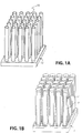
- FIG. 1A An array of conducting nanowires, 10, in electrical contact with conducting substrate, 12, is shown in FIG. 1A .
- Electrolyte material, 14, is conformal coated onto conducting nanowires 10, as shown in FIG. 1B .
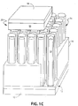
- Cathode material, 16, in electrical connection with a second conductive material, 18, is interpenetrated between electrolyte-coated nanowires 10, as shown in FIG. 1C , forming battery, 20.
- Cu 2 Sb FILMS The direct electrodeposition of crystalline, stoichiometric Cu 2 Sb films from aqueous solution at room temperature directly onto copper electrodes at a single potential is first described.
- Cu 2 Sb films were electrodeposited from aqueous 0.4 M citric acid solutions (denoted H 3 Cit, 99.5+% Aldrich) containing 0.025 M antimony (III) oxide (Sb 2 0 3 , nanopowder, 99.9+% Aldrich), and 0.1 M copper (II) nitrate hemipentahydrate (Cu(NO 3 ) 2 , 99.9+% Aldrich), prepared by adding the citric acid to Millipore water (18 ⁇ ) followed by the addition of Sb 2 O 3 . The complete dissolution of the Sb 2 0 3 was aided by mechanical stirring after which the Cu(N0 3 ) 2 was added.
- the pH was then raised to 6 by the addition of 5 M potassium hydroxide (KOH, ACS certified, Fisher).
- KOH potassium hydroxide
- the Cu 2 Sb films were obtained by performing bulk electrolysis at room temperature at a potential of -1050 mV versus a saturated sodium calomel electrode (SSCE). The temperature and the potential were also systematically varied in order to find the optimal deposition conditions. Cyclic voltammograms (CVs) and depositions were conducted using a three-electrode cell and a potentiostat. Platinum gauze was used as a counter electrode, and a SSCE (0.236 V versus the standard hydrogen electrode) was used as the reference electrode.
- a platinum disk electrode (1.7 mm 2 ) or a glassy carbon electrode (7.0 mm 2 ) was used as the working electrode for the CVs, and copper or gold flag electrodes for the depositions.
- the copper flags were copper foil (0.25 mm thick, 99.98% Aldrich) with an area of 2-4 cm 2 , and were mechanically polished using diamond paste and electrochemically polished in phosphoric acid (H 3 PO 4 , 85%, Mallinkrodt Chemicals) at a current of 0.15 A for less than 5 s.
- the gold substrates were made using a vacuum evaporator with a deposition controller. Approximately 10 nm of chromium was evaporated onto glass slides as an adhesion layer, followed by 300 nm of gold.
- Citric acid is a triprotic acid; therefore, solutions of varying pH were examined using cyclic voltammetry to study the effect of pH on the copper and antimony deposition potentials.
- Solutions containing Cu(N0 3 ) 2 , Sb 2 O 3 , and citric acid were made ranging from pH 1 to 8. The concentrations of Cu 2+ and Sb 3+ were 0.1 M and 0.05 M, respectively (before the addition of KOH).
- Cyclic voltammograms (CVs) were taken from pH 1 to pH 8, inclusively, using 0.1 M Cu(NO 3 ) 2 and 0.025 M Sb 2 0 3 (i.e. 0.05 M Sb 3+ ) in 0.4 M citric acid taken using a SSCE reference electrode, a platinum working electrode, and with a scan rate of 250 mV/s.
- the CV of citric acid alone exhibits two reduction peaks; one due to a surface phenomenon on Pt (at -118 mV) and one (at -750 mV) due to the reduction of a citrate species.
- the CVs of each metal individually indicate that the Cu 2+ reduction peak shifts in the negative direction while the Sb 3+ reduction peak shifts in the positive direction.
- Deposition at a single potential results in the formation of Cu 2 Sb.
- a large oxidation peak is observed at 125 mV, corresponding to the stripping of Cu 2 Sb. Only a single oxidation peak is observed, indicating that there is primarily a single oxidation process occurring at this potential.
- An effective concentration of citric acid for the deposition solution was determined by varying the concentration between 0.2 - 0.8 M, in solutions containing 0.05 M Sb 3+ and 0.1 M Cu 2+ separately. As the concentration of citric acid was increased, the current of the copper cathodic peak decreased. This can be attributed to the equilibrium of the copper citrate complexes; that is, as more citric acid is added, the availability of free copper ions in solution decreases. No difference in the anodic or cathodic current was observed for the antimony solutions, although sufficient citric acid should be present to complex all the antimony in order to prevent the precipitation of Sb 2 O 3 .
- the Cu substrate is responsible for the high intensity of three peaks at 43, 50 and 74° 2 ⁇ , indexed to the copper (111), (200) and (220) reflections.
- Three additional peaks were observed in the XRD pattern of the film deposited at -800 mV. All three of these peaks match peaks for Cu 2 Sb, one of which is generally used as the fingerprint for the desired compound (the broad (003) peak at 44° 2 ⁇ ).
- the film deposited at -900 mV shows larger features than the film deposited at -1000 mV.
- the grain sizes of the film deposited at -1000 mV are also smaller than the film deposited at -900 mV.
- the film grown at -900 mV is composed of grains that have an average size of 90 nm, while the average size of the grains of the film deposited at -1000 mV is 35 nm.
- the morphologies of the films deposited at -1100 and -1200 mV are consistent with the differences between their XRD patterns and those of the films deposited at -900 and -1000 mV.
- An SEM image of the film deposited at -1100 mV, the pH 6 deposition solution containing 0.1 M Cu(N0 3 ) 2 , 0.025 M Sb 2 0 3 and 0.4 M citric acid, shows dendritic growth.
- the observed diameter of the rods was found to range from 50 to 150 nm with lengths greater than 600 nm.
- the average particle size calculated from peak broadening was 50 nm, corresponding to the smallest observed diameter from SEM.
- An SEM image of the film deposited at -1200 mV shows small spherical particles (200 nm) on the surface of the film with a calculated grain size less than 20 nm.
- XRD patterns of films deposited from -1100 to -1200 mV can be indexed for Cu 2 Sb and have the predicted relative intensities.
- orientation is observed to be a function of deposition potential: films deposited at potentials more negative than -1100 mV have (111) orientation versus the films deposited at -900 and -1000 mV, which exhibit (001) orientation.
- the presence of oxide phases or amorphous inhomogeneities in the as-deposited films was investigated.
- a film for which an XRD was recorded was annealed for 5 h under argon at 220 °C.
- the peak positions observed in both XRD patterns match except that small peaks observed in the unannealed film are not present after annealing, which is consistent with the removal of surface oxide phases.
- Mn 2 Sb and MnSb are analogous to that of Cu 2 Sb during Li intercalation.
- MnSb has been shown to deliver a rechargeable capacity of 330 mAh/g.
- the lithiation of Mn 2 Sb proceeds directly to Li 3 Sb with very little LiMnSb formation, then cycles almost identically to MnSb, but with excess Mn present (as determined by in situ X-ray diffraction). Deposition of Mn 2 Sb in a manner similar to Cu 2 Sb was attempted.
- Electrodeposition into templates has been used to synthesize varies materials on a nanoscale with a wide range of applications.
- One surface thereof may be coated with a conducting metal such as gold using thermal evaporation, as an example, by first coating the surface with about 10 nm of Cr followed by about 200 nm of Au to which is attached a copper wire using silver paint.
- Nanowire material may then be electrodeposited into the pores, and the template dissolved leaving free-standing, well-ordered, equivalent-diameter nanowires. Removing the alumina template was accomplished, using both sodium hydroxide (1 M) and phosphoric acid (3 M).
- similar templates may be used for creating nanowires of conducting metals such as copper, gold, or platinum for use as templates for analysis of electrolyte deposition.
- EDS spectral maps of the resulting wires exhibit a composition gradient which is uniform over large distances.
- FIGURE 2 illustrates a sample square wave effective for the pulsed electrodeposition of Cu 2 Sb nanowires, where the deposition potential (Ef) was the same potential as used in the electrodeposition of films (-1.05 V versus SSCE).
- the deposition potential (Ef) was the same potential as used in the electrodeposition of films (-1.05 V versus SSCE).
- pulse deposition pulse plating
- T on the on time
- T off the off/reverse time
- the concentration gradient established during T on dissipates during T off. This should allow for more uniform wire growth and pore filling while limiting composition effects that are created by local concentration gradients established in the pores.
- T v on the time axis represents the fact that T off may be varied to obtain the desired wire uniformity.
- Platinum gauze was used as the counter electrode, and a SSCE (0.236 V versus the standard hydrogen electrode) was used as the reference electrode.
- a platinum disk electrode (2.01 mm 2 ) was used as the working electrode for the CVs, and the copper or gold electrodes for the film depositions.
- the working electrodes for the film deposition were either copper or gold evaporated onto glass slides.
- the substrates were made using a vacuum evaporator with a deposition controller. Approximately 10 nm of chromium were evaporated onto glass slides as an adhesion layer, followed by 300 nm of copper or gold. Electrical contact was made by connecting a copper wire with an alligator clip.
- Electropolymerization is an effective method for creating conformal coatings without pinhole defects on high-area electrodes for batteries.
- the control of the thickness of the polymer layer may create an electrically resistive, ionically conducting barrier suitable for avoiding electrical shorts, inhomogeneous electric fields and inhomogeneous ionic diffusion rates.
- the electropolymerization of po/y-[Zn(4-vinyl-4'methyl-2,2'-bipyridine) 3 ](PF 6 ) 2 results in the conformal coating of high aspect ratio nanowire arrays without the presence of pinhole defects.
- [Zn(4-vinyl-4'methyl-2,2'-bipyridine) 3 ](PF 6 ) 2 was chosen since: (a) the complex's metal-based oxidation, Zn +2/+3 , requires a high potential, making it an alternative to the well-studied redox active ruthenium and osmium analogs; (b) the large electroinactive window of the polymer enables the separation of the electrodes to prevent shorting; and (c) the electropolymerization of the zinc tris (vbpy) complex is a reduction-based polymerization achieved by applying a negative potential to inject electrons into the bipyridine rings.
- Atomic force microscopy, AFM, in contact mode was used to establish the thickness of the polymer films as a function of cycle number. Thickness was measured across scratches made in the polymer film with a razor blade. With a monomer concentration of 1 mM, and an electrode surface area of 0.1 cm 2 , the thickness of the polymer film was found to vary linearly with cycle number up to twenty cycles. This correlation is not rigorous on nanowires due to the inherent differences in diffusion profiles when depositing on nanowires versus a planar electrode; however, it is a useful guide for estimating the number of cycle numbers required to achieve an approximate thickness. Polymer coatings deposited on both films and nanowire arrays were examined.
- AAO porous anodic aluminum oxide
- a thick layer of gold or copper was first evaporated onto one side of an AAO template, a copper wire was attached with silver paint, and the entire metal surface on the back of the AAO was painted with water insoluble, electrically insulating nail polish. Copper wires were then deposited in the AAO pores, and the alumina template was selectively dissolved away, resulting in free-standing wires.
- the electrodes were constructed by placing the AAO on a strip of conducting ITO glass (13 ⁇ ) and the surrounding ITO covered with a non-conducting epoxy (TorrSeal) which is inert to acetonitrile. Scanning electron microscopy images of the copper wires before and after polymerization exhibit a uniform change in morphology for the coated wires versus the as-deposited nanowires; that is, the nanowires were all uniformly thicker after the deposition process. However, imaging techniques are insensitive to low numbers of defects.
- Redox shut-off experiments were conducted with similarly synthesized platinum nanowires since this technique should be sensitive to pinholes in the polymer coatings.
- Redox activity of two species having different sizes and charges was investigated: the smaller, neutral ferrocene exhibits electroactivity on the polymer-coated electrodes, albeit significantly attenuated relative to each corresponding bare electrode, with a wave shape consistent with restricted diffusion ostensibly through the molecular-dimension pores of the polymer.
- the redox activity of the larger, positively charged [Ru(2,2',2"-terpyridine) 2 ] 2+ species appears to be blocked on both the planar and nanowire electrodes coated with polymer.
- the voltammetric response of cobaltocenium was also measured and found to be similar to ferrocene. Electrochemical tests, coupled with the SEM micrographs indicate that a conformal layer of poly -[Zn(4-vinyl-4'methyl-2,2'-bipyridine) 3 ](PF 6 ) 2 is deposited on the surface of the nanowires. A micrograph of the entire length of a polymer modified copper nanowires, showed that the morphology and contrast is the same along the entire length of the nanowires, indicating complete coverage. The same polymer has also been shown to grow on and adhere well to copper, platinum, gold, and ITO surfaces. Therefore, it is expected that this polymer will deposit well on Cu 2 Sb nanowires.
- X-ray photoelectron spectroscopy was used to further confirm the presence of the polymer coating on both nanowires and films.
- the presence of the Zn 2p 3/2 and F 1s peaks were used as the fingerprints for the presence of the polymer, and representative peaks for each metal were probed on bare electrodes for comparison. Clear metal peaks are observed before coating, and a complete lack of the metal peaks were observed for polymer coated nanowires and films.
- a series of polymer-modified patterned ITO electrodes were tested to examine the breakdown voltage as a function of polymer thickness. A ⁇ 30 nm polymer layer electrodeposited on patterned ITO showed no appreciable current flow up to its breakdown bias of ⁇ + 3.5 V, which indicates that a thin polymer layer is electrically resistive over a large voltage window.
- the polymer films disclosed herein are useful as solid-state electrolyte materials for use in electrochemical cells, such as lithium-ion batteries. This is largely due to their high ionic conductivity and low electronic conductivity. These films are particularly useful in batteries with very small scale features (such as nanoscale) because they can be conformally deposited using an electroreductive polymerization method. This method results in good uniformity of film thickness without large numbers of pinholes and other defects, making the film of sufficient quality that the film is suitable for application as an electrolyte in a lithium-ion battery.
- Reductive electropolymerization is well-known in the art, including the reductive polymerization of vinyl monomers.
- the first step in fabricating the films disclosed herein is to electrochemically reduce a vinyl monomer, in particular an acrylate-based monomer (including methacrylates, methacrylic acid, acrylic acid, acrylamide, methacrylamide, vinyl acetate and related), and specifically tetramethylammonium 3-sulfopropyl acrylate (TPASPP), lithium 3-sulfopropyl acrylate (LiSPP), and glycidal methacrylate (GYM).
- GYM glycidal methacrylate
- An advantage of GYM is that it contains heteroatoms (namely oxygen) that can assist in the conduction of lithium ions.
- An advantage of SPP-based films is that the presence of a covalently bound anion can assist in the conduction of lithium cations by virtue of offering a charge-compensating anion.
- Electrochemical reduction of these monomers will initiate the polymerization of these monomers.
- a solid film will be deposited on the surface of the electrode as the polymer chain grows.
- the specific conditions employed may be used to determine the properties of the film (e.g. thickness, uniformity). Common techniques include stepping to a defined voltage and potentiometric cycling of the electrode.
- Reductive electropolymerization permits conformal deposition of polymeric films of controlled and generally uniform thickness onto an electrode surface with morphological features of either very small size (for example, nanoscale dimensions) and/or irregular or complex patterning.
- this technique may be used to generate films on nanowires, nanotubes, and related nanostructures which have been previously fabricated on the electrode surface (for example, Cu 2 Sb nanowires), when the electrolyte is required to be thin and conformal so that the battery cathode material can be deposited in and among the nanowires.
- Li+ doping after treatment may be required to enable sufficient ionic conduction and to introduce lithium ion into the system. It is believed that the ionic conduction of polyGYM derives from etheral oxygens having a slight negative charge sufficient to attract Li + (similar to PEO doping). It has been observed by the inventors that when polyGYM is soaked in 1M LiClO 4 (in propylene carbonate, or PC) for 48 h, dip-rinsed, and the PC removed in vacuo at ⁇ 70 °C, the polymer may be doped to form LiClO 4 : polyGYM, as may be corroborated using high-resolution XPS.
- 1M LiClO 4 in propylene carbonate, or PC
- any film produced from monomers with cations other than lithium may require a cation exchange procedure (e.g. exchanging K + for Li + , or TMA + for Li + ).
- Cation exchange is a technique well-known to those skilled in the art and may be accomplished in a number of ways, for example, the soaking procedure described above for polyGYM, perhaps repeated two or more times, would be expected to result in successfully ion exchange.
- lithium cobalt oxide Materials found useful for large-scale lithium batteries including lithium cobalt oxide, lithium magnesium oxide, or lithium tin oxide, are expected to be effective for the present lithium ion battery. Although each of these materials has a theoretical capacity, the actual capacities of the bulk materials are much smaller (110 for cobalt, 150 for manganese, and 270 for tin). The capacities are expected to be greater when used on a nanoscale due to a higher surface area to volume ratio, and the greater ability of the nanowires to withstand the volume expansion and contraction that results in pulverization of the bulk materials. These materials were synthesized using a sol gel method in alumina templates. Such methods begin with dissolving precursors in solution. The space between the coated nanowires in the battery structure is filled with the solution.
- a slow reaction forming a sol occurs, the sol densifying in time to form a gel.
- Alcohol may be added to the solution, the ratio of water to alcohol in the initial solution being useful for controlling the gelation time of the sol.
- the gel is annealed at a chosen temperature to generate a powder which uniformly coats the nanowires.
- the second electrode may then be placed in electrical contact with the powder by a number of well-known methods, such as thermal evaporation of a metallic species, as an example.
- the thickness of the cathode material may be matched to the amount of lithium in the anode material.
- Lithium cobalt oxide LiCoO 2
- Equal molar quantities of lithium acetate (Aldrich, 99.99%) and cobalt (II) acetate (Aldrich, 98%) were mixed in a 4:1 molar solution of Ethylene glycol (Fisher Scientific, lab grade) and citric acid (Sigma-Aldrich, analytical grade).
- the solution was then heated to 140 °C for 5 h while stirring, until a pink gel was formed, to induce esterification, and then left to cool.
- the solution may be poured onto the nanorods or the nanorods may be dipped into the solution as it is becoming a gel over time, followed by a low-temperature anneal.
- the powdered materials may then be generated by heating the annealed gel to higher temperatures.
- Samples were prepared either on glass slides or on 100 nm sized porous alumina templates (Whatman Filters, anodisc 13, 0.1 ⁇ m) and placed in a vacuum at 60 °C for 1 h. For the templates this process was repeated multiple times to ensure proper filling of the pores. The samples were then placed in the oven and heated for 16 h to 550 °C with an increase in temperature of 0.3 to 1 °C per min. Porous alumina templates were employed to simulate high-aspect ratio structures, such as nanowires. At temperatures below 500 °C the pink/red samples created a glass like phase in which no powder was obtained; above 550 °C, powders effective for use as cathode materials were generated.
- Lithium manganese oxide ((LiMnO 2 FCC, Li 0 . 82 [Mn 1.7 Li 0 . 3 ]O 4 monoclinic)):
- Lithium manganese oxide was prepared in the same manner except that manganese (II) acetate (Aldrich, 98%) replaced the cobalt acetate. Samples were obtained on glass slides for the lithium manganese oxide gel. At temperatures below 200 °C the brown samples created a glass like phase in which no powder was obtained.
- Lithium tin oxide Li 2 SnO 3
- Lithium tin oxide was prepared in the same manner except that tin (II) chloride (Sigma Aldrich, reagent grade) replaced the cobalt acetate. Samples were obtained on glass slides for the lithium tin oxide gel, all temperatures producing a white powder.
- tin (II) chloride Sigma Aldrich, reagent grade
- LiFePO 4 Phosphates such as LiFePO 4 , as an example, may also be used, which may exhibit higher voltages and longer lifetimes than typical oxides.
- the lithium ferrous phosphate may be doped with cobalt, aluminum or magnesium.
Description
- Described herein are batteries and, more particularly lithium-ion batteries.
- Lithium is the lightest and most electropositive element, making it well-suited for applications that require high energy density. As such, lithium-ion (Li+) batteries have been successfully employed in a large variety of portable and other electronic devices. However, slow diffusion of Li+ into the anode and the cathode, as well as slow diffusion between the two electrodes, remain the two principal limitations to the rates of charging and discharging for these batteries.
- Nanostructured materials have been demonstrated to be useful for Li+ batteries due to their high surface area-to-volume ratio, a property that has been shown to lead to greater reversibility for the lithiation reaction and greater discharge rates. Moreover, fabrication of nanowire arrays of both carbon-based anodes and several common cathode materials has been shown to enhance electrode performance because the reduction in particle size of the electrode materials, while maintaining electrical contact from grain to grain, reduces the distances the Li+ ions must diffuse.
- In particular, the charge/discharge rate of a battery is related to the rates of diffusion of Li+ into each electrode and the rate of diffusion between the cathode and the anode. While nanowires have been shown to cycle faster than bulk materials, reducing the distance between cathode and anode battery structures has not been straightforward, and although nanostructured cathodes/anodes have previously been utilized in Li+ batteries, this was done primarily to increase the surface area-to-volume ratio of either the cathode or anode or both, and the Li+ diffusion distance remained, as a consequence, quite large as lithium ions were required to travel large distances between macroscopically separated electrodes.
US2750333A relates to electrodeposition of antimony and antimony alloys.GB1224507A JP2005206915A - According to an aspect of the invention, provided herein is a method for electrodepositing stoichiometric, crystalline copper antimonide onto an electrically conducting substrate at room temperature, comprising: preparing a solution having a chosen molar concentration of Cu2+ and a chosen molar concentration of Sb3+ in an aqueous solution comprising citric acid, wherein the chosen molar concentration of Cu2+ is twice the chosen molar concentration of Sb3+; adjusting the pH of the solution to pH 6 such that the difference between the reduction potential of the Sb3+ to Sb and the reduction potential of Cu2+ to Cu is minimized; and applying a negative potential to the electrically conducting substrate; such that stoichiometric Cu2Sb is electrodeposited onto the substrate.
- Described herein is a lithium-ion battery effective for increasing the diffusion rate of Li+ between the battery anode and cathode.
- Also described herein is a lithium-ion battery effective for increasing the rate of diffusion of Li+ into the battery anode and cathode.
- Additional objects, advantages and novel features of the invention will be set forth in part in the description which follows, and in part will become apparent to those skilled in the art upon examination of the following or may be learned by practice of the invention. The objects and advantages of the invention may be realized and attained by means of the instrumentalities and combinations particularly pointed out in the appended claims.
- To achieve the foregoing and other objects, as embodied and broadly described herein, the lithium-ion battery, hereof, includes in combination: an anode including electrodeposited structures having intermetallic composition effective for reversibly intercalating lithium ions, the structures being in electrical communication with a first electrode; a lithium-ion conducting solid-state electrolyte deposited on the structures of the anode; and a cathode material interpenetrating the space between the structures of the anode in electrical communication with a second electrode.
- Also described herein, and in accordance with its objects and purposes, the method for producing a lithium-ion battery, hereof, including the steps of: forming an anode comprising electrodeposited structures having intermetallic composition effective for reversibly intercalating lithium ions, the structures being in electrical communication with a first electrode; depositing a lithium-ion conducting solid-state electrolyte on the structures of the anode; and interpenetrating the space between the structures of the anode with a cathode material in electrical communication with a second electrode.
- Also described herein, and in accordance with its objects and purposes, an electrode including electrodeposited structures having intermetallic composition.
- Benefits and advantages described herein include, but are not limited to, providing a battery having nanoscale dimensions wherein the electrodes are interpenetrating, thereby significantly reducing the distance which the Li+ ions are required to traverse upon charging/discharging of the battery over other types of lithium-ion batteries.
- The accompanying drawings, which are incorporated in and form a part of the specification, illustrate the embodiments of the present invention and, together with the description, serve to explain the principles of the invention. In the drawings:
-
FIGURES 1A - 1C illustrate a method for assembling the battery described herein, wherein the step of generating an anode including an array of conducting structures in electrical contact with a conducting substrate is shown inFIG. 1A; FIG. 1B shows the step of placing a conformal coating of an electrolyte material onto the conducting structures shown inFIG. 1A hereof; and the step of interpenetrating cathode material between the anode structures in electrical connection with a second conductive substrate is shown inFIG. 1C . -
FIGURE 2 illustrates a sample square wave effective for the pulsed electrodeposition of Cu2Sb wires, where the deposition potential (Ef) was the same potential as used in the electrodeposition of Cu2Sb films (-1.05 V versus SSCE). - Briefly, described herein is a lithium-ion (Li+) battery having an anode comprising an array of nanowires electrochemically coated with a polymer electrolyte, and surrounded by, and in electrical communication with a cathode matrix, forming thereby interpenetrating electrodes, and a method for producing such batteries. The present battery architecture increases the diffusion rates of the Li+ between the cathode and anode by reducing the Li+ diffusion length between these two electrodes. Small, lightweight batteries having long lifetimes, and capable of rapidly discharging power may be constructed.
- In accordance with embodiments described herein, an array of high aspect-ratio nanostructures (such as nanowires, nanoribbons, nanotubes, and nanocones, as examples) having dimensions (for example, length) such that one dimension may be 10 to 1000 times larger than a smaller dimension (for example, the diameter of a wire) which may have nanometer-scale dimensions, may be formed on conductive, generally planar substrates. Nanorods, having an aspect ratio of less than 10 may also be formed. In what follows the term "nanowire" will be utilized as exemplary of "nanostructures."
- Dendritic growth of metallic lithium onto the commonly used graphite anodes can lead to shorting in the battery and may cause safety issues. Therefore, new anode materials and morphologies are desired in which these safety issues, as well as the capacity and the charge/discharge rates, can be improved over graphite. Intermetallic compounds offer the possibility of improved capacity, a highly reversible reaction with lithium, and a lithium intercalation potential that may be less negative than the deposition potential of metallic lithium, the latter property being useful for eliminating dendritic growth of elemental lithium on the electrode. A drawback of using intermetallics as anode materials has been the irreversible loss in capacity during cycling due to large volume changes which result in pulverization of the electrode during cycling and, consequently, a loss of electrical contact between the anode and the remainder of the battery. Cu2Sb is an intermetallic composition that does not exhibit large volume changes during the charging and discharging. Another benefit of Cu2Sb is that its operating potential precludes lithium metal plating. The use of Cu2Sb nanowires has an additional benefit in that electrodes having nanoscale dimensions generally provide immunity from pulverization resulting from large volume changes, even over electrodes having micron scale dimensions.
- As will be described hereinbelow, Cu2Sb may be directly deposited onto a conducting substrate with precise control of composition and thickness under mild conditions, and onto complex shapes and into deep recesses with excellent electrical contact without requiring post-annealing. Codeposition of Cu and Sb from aqueous solutions presents two challenges: the reduction potentials of Cu and Sb differ by approximately 130 mV in aqueous solutions, and the deposition of Cu is preferred at less negative potentials; and while antimony salts are soluble in acidic solutions, they precipitate in neutral aqueous solutions to form Sb2O3. The electrodeposition of Sb is not possible in acidic solutions because H2 is formed from the reduction of H2O, at less negative potentials than those required to reduce Sb3+. Citric acid (C6H8O7) is used to keep Sb3+ in solution in less acidic solutions and/or shift its reduction potential to less negative potentials. Citric acid has been used as a complexing agent in deposition solutions for copper and antimony separately, due to its three carboxylic acid groups and one hydroxyl group. The resulting complexation of the Sb3+ by the citrate species in solution allows the pH to be raised without the formation of Sb2O3, and results in a widening of the electrochemical window of the solution and shifted toward more negative potentials.
- The direct electrodeposition of the intermetallic composition, Cu2Sb, from aqueous solutions containing the required stoichiometric amount of copper versus antimony (for Cu2Sb) has been achieved using citric acid as a complexing agent, thereby increasing the solubility of antimony salts and shifting the reduction potentials of copper and antimony toward each other, and enabling the direct deposition of the intermetallic compound at room temperatures and at a pH = 6. The electrodeposition was performed onto copper substrates resulting in a Cu2Sb thin film that is homogeneous, stoichiometric and crystalline.
- One embodiment of the present method utilizes anodic aluminum oxide (AAO) technology to form an array of channels in the alumina substrate. Cu2Sb is deposited into the nanochannels at a single electrochemical potential. The intermetallic compound, Cu2Sb, displays excellent properties for use as an anode in Li+ batteries: (a) increased charge storage capacity; (b) increased charging and discharging rates; and (c) reduced hazard of plating lithium metal onto the anode. Other intermetallic compounds also display these properties and may function equally well as anodes. Once a suitable anode material is deposited into the nanochannels, the AAO template is removed using standard chemical techniques. The remaining array of nanostructures (Cu2Sb nanowires, in the present case) functions as a nanostructured anode having a high surface area. The nanostructures generated may display a high aspect ratio, generally having dimensions on the order of a few nanometers to several hundred nanometers in diameter and tens of nanometers to several hundred micrometers in length.
- An electrically-insulating polymer may then be deposited onto the anode, conformally coating the nanowires and serving as the battery electrolyte. The electrolyte's function is to allow passage of Li+ while offering a high resistance to electrical conduction (i.e., the passage of electrons or electrical current). Although any insulating material capable of conducting Li+ is suitable, it should be applied in a generally conformal manner as a very thin layer which does not significantly modify the nanowire shapes within the array. One example is an electrochemically deposited poly(pyridine)zinc polymer prepared from [tris(4-methyl-4'-vinyl-2,2'-bipyridine)Zn](PF6)2) using a reduction technique, although other insulating polymers could be deposited electrochemically or otherwise by procedures known to those skilled in the art (including polyethylene carbonate derivatives). The thickness and material of the electrolyte is chosen such that the electrolyte is substantially electrically insulating but the nanowire shape is not substantially distorted. An insulating material, which may be the same material as that used for the conformal electrolyte coating, but may be any other electrically insulating material, covers exposed surfaces of the planar conductive substrate. Typically, the thickness of the electrolyte may be between about one nanometer and about a few hundred nanometers.
- A cathode material may be introduced such that the coated nanowires in the array are further covered, and electrical contact made with a second electrode. Any suitable Li+ battery cathode material may be used with LiCoO2, LiMnO2, and Li2SnO3, or phosphates, as examples. Such materials may be deposited in a number of ways. A sol-gel method, to be described hereinbelow, permits uniform distribution of the cathode material into the coated nanowire array.
- Intermetallic materials having similar crystal structures to their lithiated counterparts have been sought since, with both the parent and product crystal structure being similar, less rearrangement is needed during the charging and discharging of the material, thereby reducing the volume change. Copper antimonide is one such intermetallic, with the antimony atoms in a face center cubic array in both the parent and product crystal structures. The similarity in crystal structures leads to an overall volume change of 95% upon lithiating Cu2Sb to Li3Sb (compared to 300% for Sn). The improvement in cycle life of Cu2Sb has been demonstrated, maintaining a capacity of 1914 mAh ml-1 after 35 cycles. Further, nanowires of Cu2Sb should be less prone to degradation during charging and discharging than graphite, because of the inherent properties of the material and the nanoscale dimensions of the wires.
- Previous investigations into the battery performance of Cu2Sb involved using slurries of the active material mixed with a binder and carbon black since the binder is used to attach the powder to an electrode, thereby making electrical contact, and allows the material to undergo significant volume change without losing electrical contact with the current collector. To reproduce this soft matrix, a thin layer of graphite was evaporated onto a copper substrate, and then Cu2Sb was electrodeposited onto the graphite. The graphite acted as a "soft" interface, which accommodates the volume change of the Cu2Sb while keeping the electrical contact to the substrate. A steady capacity of 200 mAhg-1 was maintained, whereas in the case of Cu2Sb on Cu the capacity falls dramatically during the first few cycles until it reaches a minimum of 24 mAhg-1. The graphite was found to improve the reversible capacity by an order of magnitude. Cycling capacity was also investigated as a function of film thickness. As the film gets thinner, the capacity of the film has been found to be maintained for a greater number of cycles. Nanowires of Cu2Sb are expected to have an even greater ability to maintain capacity upon repeated cycling since the micron thickness of the prepared films is greater than the radius of the nanowires. Moreover, strain due to volume changes is better accommodated in a nanowire where it is constrained only in the longitudinal direction, than in a film where the material is constrained in all three dimensions. Thus, electrode material degradation in lithium-ion batteries may be reduced by using nanoscale morphology since materials having small dimensions survive longer than bulk materials.
- Reference will now be made in detail to the present embodiments of the invention, examples of which are illustrated in the accompanying drawings. In the Figures, similar structure will be identified using identical reference characters. Turning now to
FIGURES 1A - 1C a method for assembling the battery described herein is illustrated. An array of conducting nanowires, 10, in electrical contact with conducting substrate, 12, is shown inFIG. 1A . Electrolyte material, 14, is conformal coated onto conductingnanowires 10, as shown inFIG. 1B . Cathode material, 16, in electrical connection with a second conductive material, 18, is interpenetrated between electrolyte-coatednanowires 10, as shown inFIG. 1C , forming battery, 20. - Having generally described the invention, the following EXAMPLES provides additional details:
- A. Cu 2 Sb FILMS: The direct electrodeposition of crystalline, stoichiometric Cu2Sb films from aqueous solution at room temperature directly onto copper electrodes at a single potential is first described.
- Cu2Sb films were electrodeposited from aqueous 0.4 M citric acid solutions (denoted H3Cit, 99.5+% Aldrich) containing 0.025 M antimony (III) oxide (Sb203, nanopowder, 99.9+% Aldrich), and 0.1 M copper (II) nitrate hemipentahydrate (Cu(NO3)2, 99.9+% Aldrich), prepared by adding the citric acid to Millipore water (18 Ω) followed by the addition of Sb2O3. The complete dissolution of the Sb203 was aided by mechanical stirring after which the Cu(N03)2 was added. The pH was then raised to 6 by the addition of 5 M potassium hydroxide (KOH, ACS certified, Fisher). The Cu2Sb films were obtained by performing bulk electrolysis at room temperature at a potential of -1050 mV versus a saturated sodium calomel electrode (SSCE). The temperature and the potential were also systematically varied in order to find the optimal deposition conditions. Cyclic voltammograms (CVs) and depositions were conducted using a three-electrode cell and a potentiostat. Platinum gauze was used as a counter electrode, and a SSCE (0.236 V versus the standard hydrogen electrode) was used as the reference electrode. A platinum disk electrode (1.7 mm2) or a glassy carbon electrode (7.0 mm2) was used as the working electrode for the CVs, and copper or gold flag electrodes for the depositions. The copper flags were copper foil (0.25 mm thick, 99.98% Aldrich) with an area of 2-4 cm2, and were mechanically polished using diamond paste and electrochemically polished in phosphoric acid (H3PO4, 85%, Mallinkrodt Chemicals) at a current of 0.15 A for less than 5 s. The gold substrates were made using a vacuum evaporator with a deposition controller. Approximately 10 nm of chromium was evaporated onto glass slides as an adhesion layer, followed by 300 nm of gold. Electrical contact was made by connecting a copper wire to the flags with carbon paint or with a clip. Clear nail polish was used to insulate the edges of the substrate and the back of the copper foil in order to ensure that deposition only occurred on flat surfaces with a controlled surface area. The depositions were carried out at a constant potential for 10 min. periods. The films were rinsed with Millipore water and allowed to air dry.
- Citric acid is a triprotic acid; therefore, solutions of varying pH were examined using cyclic voltammetry to study the effect of pH on the copper and antimony deposition potentials. Solutions containing Cu(N03)2, Sb2O3, and citric acid were made ranging from pH 1 to 8. The concentrations of Cu2+ and Sb3+ were 0.1 M and 0.05 M, respectively (before the addition of KOH). Cyclic voltammograms (CVs) were taken from pH 1 to pH 8, inclusively, using 0.1 M Cu(NO3)2 and 0.025 M Sb203 (i.e. 0.05 M Sb3+) in 0.4 M citric acid taken using a SSCE reference electrode, a platinum working electrode, and with a scan rate of 250 mV/s.
- In addition to significantly increasing the electrochemical window of the solution, raising the pH also controls which citrate species are present. Whereas at pH = 1 the predominant species present for the citrate is the fully protonated species (denoted H3Cit), at pH = 6 there is a mixture of HCit2- and Cit3-. Once the electrochemical window is extended toward more negative potentials, the difference between the reduction potentials of the metal species in solution is minimized at pH = 6, which pH has the additional advantage that slightly acidic pH conditions preclude oxide precipitation during film deposition. A CV of the pH = 6 solution was found to exhibit a large cathodic peak at -950 mV, which may be attributed to the reduction of a copper citrate dimer, followed by a shoulder located at -1150 mV corresponding to the reduction of Sb3+.
- The CV of citric acid alone exhibits two reduction peaks; one due to a surface phenomenon on Pt (at -118 mV) and one (at -750 mV) due to the reduction of a citrate species. As the pH is increased from 1 to 6, the CVs of each metal individually indicate that the Cu2+ reduction peak shifts in the negative direction while the Sb3+ reduction peak shifts in the positive direction. Deposition at a single potential (-1050 mV) results in the formation of Cu2Sb. Upon switching the scan direction, a large oxidation peak is observed at 125 mV, corresponding to the stripping of Cu2Sb. Only a single oxidation peak is observed, indicating that there is primarily a single oxidation process occurring at this potential. Thus, copper metal is not deposited when Cu2+ alone is complexed by citrate at pH = 6; however, in the presence of antimony citrate two reduction peaks are observed with the result that Cu2Sb is deposited.
- An effective concentration of citric acid for the deposition solution was determined by varying the concentration between 0.2 - 0.8 M, in solutions containing 0.05 M Sb3+ and 0.1 M Cu2+ separately. As the concentration of citric acid was increased, the current of the copper cathodic peak decreased. This can be attributed to the equilibrium of the copper citrate complexes; that is, as more citric acid is added, the availability of free copper ions in solution decreases. No difference in the anodic or cathodic current was observed for the antimony solutions, although sufficient citric acid should be present to complex all the antimony in order to prevent the precipitation of Sb2O3. To avoid the precipitation of Sb2O3, forming 0.05 M Sb3+ solutions, the minimum amount of citric acid needed was found to be about 0.4 M. Because lower concentrations of citric acid are desired for the copper deposition and at least 0.4 M citric acid is needed to keep Sb3+ in solution, 0.4 M citric acid was determined to be an effective citric acid concentration. All solutions used for subsequent discussions contain 0.1 M Cu(N03)2, 0.025 M Sb2O3, and 0.4 M citric acid adjusted to pH = 6.
- Using the solution conditions set forth hereinabove, an investigation of the deposition parameters was conducted. Films were deposited at different potentials surrounding the cathodic peaks: the five potentials chosen were -800 mV (the onset of the first cathodic peak), -900 mV, -1000 mV (the first peak maximum), -1100 mV (the onset of the second peak), and -1200 mV. Compositional results determined by X-Ray Photoelectron Spectroscopy, XPS, show that the ratio of Cu/Sb decreases with more negative potentials. Relative to the desired 2/1 copper/antimony ratio, copper-rich films are deposited at less negative potentials, and antimony-rich films are deposited at more negative potentials. The desired ratio was found for films deposited between -1000 and -1100 mV. This same trend was also observed in corresponding Energy-Dispersive X-Ray Spectra, EDS data.
- X-Ray diffraction (XRD) patterns were used for phase identification of the films deposited at various potentials using solutions containing 0.1 M Cu(NO3)2, 0.025 M Sb2O3, and 0.4 M citric acid at pH = 6. The Cu substrate is responsible for the high intensity of three peaks at 43, 50 and 74° 2θ, indexed to the copper (111), (200) and (220) reflections. Three additional peaks were observed in the XRD pattern of the film deposited at -800 mV. All three of these peaks match peaks for Cu2Sb, one of which is generally used as the fingerprint for the desired compound (the broad (003) peak at 44° 2θ). The absence of additional Cu2Sb peaks and the copper-rich composition determined by XPS indicates that this film is a mixture of Cu, Cu2Sb, Sb and/or a solid solution of Cu and Sb. Multiple Cu2Sb peaks appear in the XRD patterns of the films deposited at all other potentials, indicating more crystalline films. The XRD patterns of the films deposited at -900 and -1000 mV are similar, but the peaks of the film deposited at -1000 mV have higher relative peak intensities than the film deposited at -900 mV. Since all films were deposited for the same amount of time, the increased peak intensities may be due to increased crystallinity or simply greater growth rate. Although the Scanning Electron Microscope, SEM, images of these films also show similar surface morphologies, the film deposited at -900 mV shows larger features than the film deposited at -1000 mV. The grain sizes of the film deposited at -1000 mV are also smaller than the film deposited at -900 mV. As calculated by the Scherer method, the film grown at -900 mV is composed of grains that have an average size of 90 nm, while the average size of the grains of the film deposited at -1000 mV is 35 nm.
- The morphologies of the films deposited at -1100 and -1200 mV are consistent with the differences between their XRD patterns and those of the films deposited at -900 and -1000 mV. An SEM image of the film deposited at -1100 mV, the pH = 6 deposition solution containing 0.1 M Cu(N03)2, 0.025 M Sb203 and 0.4 M citric acid, shows dendritic growth. The observed diameter of the rods was found to range from 50 to 150 nm with lengths greater than 600 nm. The average particle size calculated from peak broadening was 50 nm, corresponding to the smallest observed diameter from SEM. An SEM image of the film deposited at -1200 mV shows small spherical particles (200 nm) on the surface of the film with a calculated grain size less than 20 nm. XRD patterns of films deposited from -1100 to -1200 mV can be indexed for Cu2Sb and have the predicted relative intensities. In addition, orientation is observed to be a function of deposition potential: films deposited at potentials more negative than -1100 mV have (111) orientation versus the films deposited at -900 and -1000 mV, which exhibit (001) orientation.
- No differences in Cu2Sb film composition were detectable by means of XPS for films deposited from 5 to 60 °C. The broadness of the XRD peaks decreased with increasing temperature. Also, the surface morphology of Cu2Sb films deposited at 60 °C exhibited cubic faceting.
- The presence of oxide phases or amorphous inhomogeneities in the as-deposited films was investigated. A film for which an XRD was recorded was annealed for 5 h under argon at 220 °C. The peak positions observed in both XRD patterns match except that small peaks observed in the unannealed film are not present after annealing, which is consistent with the removal of surface oxide phases.
- All films discussed thus far were deposited in 10 min. periods from unstirred solutions. Films having a thickness of 32.4 µm as determined by SEM on a cross-sectional image show no discontinuities or pores in a cross-sectional view. Excluding any nucleation time, this corresponds to an average deposition rate of 3.24 µm per minute, compared to an average of 0.72 µm per minute for the deposition of copper from a 0.2 M CuSO4 solution at a constant current of 10 mA. The observed rapid growth rate indicates that the solution parameters or interaction of the metal precursors with the substrate may facilitate the electrodeposition of Cu2Sb. To determine the importance of the substrate, films were also deposited on gold substrates. For these films the same solution parameters and deposition conditions were used. A film deposited on Au was slightly less crystalline than a film deposited on Cu, but still exhibited a (001) orientation, implying that the observed preferred orientation for films deposited at -1050 mV is not a result of templating by the substrate.
- Preliminary battery testing experiments on electrodeposited Cu2Sb films show that the as deposited films intercalate Li reversibly. All films were charged and discharged at a rate of C/3, (where C corresponds to the rate needed to discharge an electrode in 1 h). The films were first charged between the open circuit potential (ocp) to a potential below that for depositing lithium metal (2 to 0.05 V vs. Li/Li+). To reduce the degradation of the solid electrolyte interface, the films were then only discharged to 1.2 V vs. Li/Li+. Subsequent cycles were run between 1.2 and 0.05 V vs. Li/Li+. The consequences of the volume change (94%) that occurs during the change of Cu2Sb to Li3Sb were found to be significant during the first charge. The active material was observed to slough off from the copper substrates, indicating that mechanical degradation due to self-pulverization is a significant source of capacity loss. All active material was found to be removed from the copper substrate during the first ten cycles. A potential range of 1.4 to 0.65 V vs. Li/Li+ was used to reduce the volume change (by 14 %) by only partially charging the film to Li2CuSb. This improved the capacity of the material for the first 5 cycles, but the copper substrate appeared bare by the tenth cycle. The tested films were thick (32.4 µm) which may have caused the faster degradation.
- The structural transformations of Mn2Sb and MnSb are analogous to that of Cu2Sb during Li intercalation. In particular, MnSb has been shown to deliver a rechargeable capacity of 330 mAh/g. However, the lithiation of Mn2Sb proceeds directly to Li3Sb with very little LiMnSb formation, then cycles almost identically to MnSb, but with excess Mn present (as determined by in situ X-ray diffraction). Deposition of Mn2Sb in a manner similar to Cu2Sb was attempted. Analysis of CVs shows that as the pH is increased to 6 there is only a single distinct anodic peak present (at -1.2 V) due to the metal ions in solution (and not due to citric acid itself) before the onset of hydrogen evolution. Films deposited at pH = 6 and -1.2 V indicate the codeposition of both metals, but not the intermetallic compound.
- Electrodeposition into templates (commercially available porous alumina oxide and polycarbonate templates) has been used to synthesize varies materials on a nanoscale with a wide range of applications. One surface thereof may be coated with a conducting metal such as gold using thermal evaporation, as an example, by first coating the surface with about 10 nm of Cr followed by about 200 nm of Au to which is attached a copper wire using silver paint. Nanowire material may then be electrodeposited into the pores, and the template dissolved leaving free-standing, well-ordered, equivalent-diameter nanowires. Removing the alumina template was accomplished, using both sodium hydroxide (1 M) and phosphoric acid (3 M). As will be set forth hereinbelow, similar templates may be used for creating nanowires of conducting metals such as copper, gold, or platinum for use as templates for analysis of electrolyte deposition.
- Electrodeposition of Cu2Sb nanowires into porous alumina templates in accordance with the film deposition technology described in part A of this EXAMPLE 1, at a single potential, resulted in non-uniform filling of the pores, low density of filled pores and composition gradients over short distances within the wires. By contrast, using the same solution and potentiostatic pulse deposition, EDS spectral maps of the resulting wires exhibit a composition gradient which is uniform over large distances.
-
FIGURE 2 illustrates a sample square wave effective for the pulsed electrodeposition of Cu2Sb nanowires, where the deposition potential (Ef) was the same potential as used in the electrodeposition of films (-1.05 V versus SSCE). In pulse deposition (pulse plating), there are two time parameters which may be controlled: the on time (Ton) and the off/reverse time (Toff). The concentration gradient established during Ton dissipates during Toff. This should allow for more uniform wire growth and pore filling while limiting composition effects that are created by local concentration gradients established in the pores. The "quiet" potential (Er), was varied to closely approach zero current, in order to stop the deposition for a sufficient length of time for the concentration gradient to dissipate without oxidizing previously deposited material. InFIG. 2 , Tv on the time axis represents the fact that Toff may be varied to obtain the desired wire uniformity. - Preparation of the solutions for the pulse deposition of Cu2Sb thin films and nanowires is described in part A, hereinabove. All electrochemistry was performed with a ±10 V potential range with a ±250 mA current range and the ability to measure current on the tens of picoamperes; or with a ±2.4 V potential range and ±2 mA current range with the ability to measure current down to the 100 pA. The potentiostats were controlled using commercial software. Cyclic voltammograms (CVs) and depositions were conducted using a three-electrode cell. The pulse sequence will be discussed in detail in a latter section. Platinum gauze was used as the counter electrode, and a SSCE (0.236 V versus the standard hydrogen electrode) was used as the reference electrode. A platinum disk electrode (2.01 mm2) was used as the working electrode for the CVs, and the copper or gold electrodes for the film depositions. The working electrodes for the film deposition were either copper or gold evaporated onto glass slides. The substrates were made using a vacuum evaporator with a deposition controller. Approximately 10 nm of chromium were evaporated onto glass slides as an adhesion layer, followed by 300 nm of copper or gold. Electrical contact was made by connecting a copper wire with an alligator clip.
- Using pulse potentiostatic deposition, films were deposited using different time constants (Ton & Toff) onto copper substrates. The TABLE sets forth the parameters and summarizes the results. Both Ton and Toff are considerably longer than needed to charge the double layer, created by the externally applied voltage, which exists at the electrode/electrolyte interface, and quickly dissipates. This allows any effects from charging of the double layer on the current or concentration to be neglected. It may be observed from the data that the potential found to give an approximately zero current was -0.525 V versus SSCE, which corresponds to the region of the CVs between the reduction peaks and the oxidation peaks. Films deposited with shorter Ton times had diffraction peaks matching Cu3.3Sb, while films deposited with longer Ton times had diffraction peaks matching Cu2Sb. Further, when the Toff time was varied keeping the Ton at 1.5 s the crystallinity of the Cu2Sb peaks increased with a decrease in Toff.
TABLE: Summary of parameters and results of pulse deposition of Cu2Sb films onto copper substrates; each range corresponding to five different values of the parameter. Ton Toff Er Ef Examined Parameter Trend of Results Ms ms -V -V 5-50 15-15000 -0.6 1.05 Pulse period Formation of Cu3.3Sb peak with long periods 5-50000 15-150000 0.18 1.05 Pulse period Peaks matched Cu2Sb but with different orientations 150 1500 0.45-0.525 1.05 Dead potential The best powder pattern was obtained with -0.525 V 300- 3000 1500 0.525 1.05 Ton Short Ton gave Cu3.3Sb and long Ton gave Cu2Sb 1500 150-7500 0.525 1.05 Toff Peaks matched Cu2Sb with increased crystallinity with decreased Toff 150- 7500 75-3750 0.525 1.05 Pulse period Shorter period gave oriented crystalline Cu2Sb (001) - The data show that with longer Ton times and shorter Toff times, the best X-ray diffraction (XRD) patterns are obtained; however, the crystallinity is much lower than the films previously deposited using the unpulsed electrodeposition.
- Electropolymerization is an effective method for creating conformal coatings without pinhole defects on high-area electrodes for batteries. The control of the thickness of the polymer layer may create an electrically resistive, ionically conducting barrier suitable for avoiding electrical shorts, inhomogeneous electric fields and inhomogeneous ionic diffusion rates. As will be described in this EXAMPLE 2, the electropolymerization of po/y-[Zn(4-vinyl-4'methyl-2,2'-bipyridine)3](PF6)2 results in the conformal coating of high aspect ratio nanowire arrays without the presence of pinhole defects. [Zn(4-vinyl-4'methyl-2,2'-bipyridine)3](PF6)2 was chosen since: (a) the complex's metal-based oxidation, Zn+2/+3, requires a high potential, making it an alternative to the well-studied redox active ruthenium and osmium analogs; (b) the large electroinactive window of the polymer enables the separation of the electrodes to prevent shorting; and (c) the electropolymerization of the zinc tris(vbpy) complex is a reduction-based polymerization achieved by applying a negative potential to inject electrons into the bipyridine rings. The syntheses of the ligand, 4-vinyl-4'methyl-2,2'-bipyridine (vbpy) and the zinc tris(vbpy) analogue are known. In a potential cycling polymerization using this material, the current response increases as polymer is deposited with each cycle. It is also observed that Zn(m) plating onto the working electrode occurs when potentials more negative than ~ -1.70 V vs. SSCE are applied.
- Atomic force microscopy, AFM, in contact mode was used to establish the thickness of the polymer films as a function of cycle number. Thickness was measured across scratches made in the polymer film with a razor blade. With a monomer concentration of 1 mM, and an electrode surface area of 0.1 cm2, the thickness of the polymer film was found to vary linearly with cycle number up to twenty cycles. This correlation is not rigorous on nanowires due to the inherent differences in diffusion profiles when depositing on nanowires versus a planar electrode; however, it is a useful guide for estimating the number of cycle numbers required to achieve an approximate thickness. Polymer coatings deposited on both films and nanowire arrays were examined.
- Films were made by thermal evaporation, while copper nanowire arrays were synthesized by electrodeposition of copper into porous anodic aluminum oxide (AAO). A thick layer of gold or copper was first evaporated onto one side of an AAO template, a copper wire was attached with silver paint, and the entire metal surface on the back of the AAO was painted with water insoluble, electrically insulating nail polish. Copper wires were then deposited in the AAO pores, and the alumina template was selectively dissolved away, resulting in free-standing wires. Since the nail polish used is soluble in acetonitrile (the solvent used in the electrochemical polymerization), in preparing the polymer-coated nanowires, the electrodes were constructed by placing the AAO on a strip of conducting ITO glass (13Ω) and the surrounding ITO covered with a non-conducting epoxy (TorrSeal) which is inert to acetonitrile. Scanning electron microscopy images of the copper wires before and after polymerization exhibit a uniform change in morphology for the coated wires versus the as-deposited nanowires; that is, the nanowires were all uniformly thicker after the deposition process. However, imaging techniques are insensitive to low numbers of defects.
- Redox shut-off experiments were conducted with similarly synthesized platinum nanowires since this technique should be sensitive to pinholes in the polymer coatings. Redox activity of two species having different sizes and charges was investigated: the smaller, neutral ferrocene exhibits electroactivity on the polymer-coated electrodes, albeit significantly attenuated relative to each corresponding bare electrode, with a wave shape consistent with restricted diffusion ostensibly through the molecular-dimension pores of the polymer. By contrast, the redox activity of the larger, positively charged [Ru(2,2',2"-terpyridine)2]2+ species appears to be blocked on both the planar and nanowire electrodes coated with polymer. Additionally, to determine whether the polymer is acting as an ion exclusion layer, the voltammetric response of cobaltocenium was also measured and found to be similar to ferrocene. Electrochemical tests, coupled with the SEM micrographs indicate that a conformal layer of poly-[Zn(4-vinyl-4'methyl-2,2'-bipyridine)3](PF6)2 is deposited on the surface of the nanowires. A micrograph of the entire length of a polymer modified copper nanowires, showed that the morphology and contrast is the same along the entire length of the nanowires, indicating complete coverage. The same polymer has also been shown to grow on and adhere well to copper, platinum, gold, and ITO surfaces. Therefore, it is expected that this polymer will deposit well on Cu2Sb nanowires.
- X-ray photoelectron spectroscopy (XPS) was used to further confirm the presence of the polymer coating on both nanowires and films. The presence of the Zn 2p3/2 and F 1s peaks were used as the fingerprints for the presence of the polymer, and representative peaks for each metal were probed on bare electrodes for comparison. Clear metal peaks are observed before coating, and a complete lack of the metal peaks were observed for polymer coated nanowires and films. Finally, a series of polymer-modified patterned ITO electrodes were tested to examine the breakdown voltage as a function of polymer thickness. A ~30 nm polymer layer electrodeposited on patterned ITO showed no appreciable current flow up to its breakdown bias of ~ + 3.5 V, which indicates that a thin polymer layer is electrically resistive over a large voltage window.
- A. Synthesis of 4-vinyl-4'-methyl-2,2'-bipyridine and [Zn(4-vinyl-4'-methyl-2,2'-bipyridine)3](PF6)2: The syntheses of the ligand and the zinc complex were both taken from literature. The purity was checked using 1H NMR before proceeding with electropolymerization experiments.
- B. Copper And Platinum Nanowire Generation: Porous Anodic Alumina (AAO) templates were obtained from Whatman (100 nm pores, 13 mm circles) and 3-5 nm of chromium followed by 1-1.5 µm of copper (or gold) was evaporated on one side as a back electrode. Electrical contact was made to the evaporated metal by attaching a copper wire with colloidal silver paint (Ted Pella - isopropanol based). Nanowires were deposited in a three electrode cell, with a SSCE reference electrode, a platinum mesh counter electrode and the AAO working electrode. For copper, the 10 ml reaction solution consisted of 0.627 M CUSO4 in 18 Ω (Millipore) H2O and 1 ml of concentrated H2SO4. The AAO working electrode was submerged in the reaction solution until the open-circuit potential (Eoc) remained constant over 5 min. The potential was held at 0.3 V below the Eoc for 450 s to yield copper nanowires ~5 µm in length and 100 nm in diameter. The solution was stirred during the deposition (~100 rpm) to replenish reactants to the pores of the AAO template. Platinum nanowires were prepared in a similar manner, only the 10 ml deposition solution used was a 0.01 M H2PtCl6 solution with 1 ml of HClO4 (70 wt%). The potential was cycled between +0.463 V and -0.237 V (vs. SSCE) at 0.05 V s-1 for 60 cycles to yield platinum nanowires that were ~3.5 µm long and 100 nm in diameter.
- C. Nanowire Electrode Fabrication: Once the nanowires were grown, the templates were removed from solution and thoroughly washed with distilled water and ethanol. The conducting back of the AAO electrode was then attached to the conducting side of ITO glass with water-based colloidal graphite (Aquadag, Ted Pella) and dried in vacuo for 2 h. Once dried, epoxy (TorrSeal), chemically inert in CH3CN solutions, was used to cover both the AAO template and the ITO conducting glass so that only ~1 cm2 area of the template was exposed. The epoxy was then left to dry in open air for 24 h, after which the electrode was immersed in aqueous 1 M NaOH at 50 °C for 1 h to release the nanowires. Copper and platinum nanowire electrodes were both synthesized in this manner.
- D. Electropolymerization of [Zn(4-vinyl-4'methyl-2,2'-bipyridine)3](PF6)2: Electropolymerization was achieved by utilizing a three-electrode Van Dyne cell where all oxygen was evacuated by bubbling acetonitrile-saturated nitrogen through the 0.1 M TBAPF6/CH3CN before polymerization. Additionally nitrogen was blown over the cell to minimize oxygen contamination. Oxygen evacuation was confirmed by taking a background cyclic voltamogramm between 0 V and -1.2 V vs. SSCE. In all cases, a platinum wire was used as a counter electrode and the reference electrode was a saturated sodium calomel electrode (SSCE). All electrochemical and solid-state electrical measurements were done on a CH Instruments 650 potentiostat/galvanostat.
- E. Solid-State Linear Sweep Voltammetry: Electrical measurements performed on a nanometer thick layers were adapted from methods found in the literature. A Ga-In liquid metal eutectic (Sigma-Aldrich, used as received) was used to make contact to the bare and polymer covered ITO. Tungsten wire, pre-wetted by immersion into the Ga-In eutectic for 30 s, was then used to contact the liquid metal on the surface of the electrode. All solid-state electrical measurements were done in an N2-filled glove-box and the bare ITO was positively biased.
- F. Physical characterization of polymer thin-films, nanowires and polymer-modified nanowires: Scanning electron microscopy (SEM) was utilized to characterize the nanowires, before and after polymer modification. The accelerating voltage of the electron beam was lowered to 3 keV during imaging of polymer films due to excessive charging of the non-conducting polymer. X-ray photoelectron spectroscopy (XPS) (Phi 6500) was used to characterize the surface of the different electrodes. Measurements were performed with an Electron Spectrometer for Chemical Analysis system and analyzed using commercial software. An Al monochromatic source operating at 350.0 W was scanned at an energy of 58.7 eV in intervals of 0.125 eV step-1 over the range indicated on the spectra. High resolution XPS was performed using a signal to noise ratio of at least 100:1 for the films and 50:1 for the nanowires. The thickness and topography of the polymer films were analyzed using atomic force microscopy (AFM) (Alpha NSOM with contact mode capabilities) of the as deposited films on etched ITO substrates. Analysis of the topography was achieved on an 100 µm x 100 µm area, and the height was determined using the scratch method: A clean razor was used to scratch through the polymer film to the ITO substrate and a depth profile of the scratch was taken from two scratches on three seperate electrodes to yield the mean thickness and error.
- G. "Redox shut-off" experiments: The complexes [Ru(2,2',2"-terpyridine)2](PF6)2, [Co(cyclopentadienyl)2](PF6) and [Fe(cyclopentadienyl)2] (Aldrich, used as received) were used to make a 10 mM solution in 0.1 M TBAPF6\CH3CN. The three electrode cell was comprised of a platinum mesh counter electrode, Ag/AgCl reference, and the stated working electrode. Cyclic Voltamogramms were taken at 0.05 Vs-1.
- The polymer films disclosed herein are useful as solid-state electrolyte materials for use in electrochemical cells, such as lithium-ion batteries. This is largely due to their high ionic conductivity and low electronic conductivity. These films are particularly useful in batteries with very small scale features (such as nanoscale) because they can be conformally deposited using an electroreductive polymerization method. This method results in good uniformity of film thickness without large numbers of pinholes and other defects, making the film of sufficient quality that the film is suitable for application as an electrolyte in a lithium-ion battery.
- Reductive electropolymerization is well-known in the art, including the reductive polymerization of vinyl monomers. The first step in fabricating the films disclosed herein is to electrochemically reduce a vinyl monomer, in particular an acrylate-based monomer (including methacrylates, methacrylic acid, acrylic acid, acrylamide, methacrylamide, vinyl acetate and related), and specifically tetramethylammonium 3-sulfopropyl acrylate (TPASPP), lithium 3-sulfopropyl acrylate (LiSPP), and glycidal methacrylate (GYM). An advantage of GYM is that it contains heteroatoms (namely oxygen) that can assist in the conduction of lithium ions. An advantage of SPP-based films is that the presence of a covalently bound anion can assist in the conduction of lithium cations by virtue of offering a charge-compensating anion.
- Electrochemical reduction of these monomers, under the appropriate conditions (e.g. supporting electrolyte, solvent, counter/auxiliary electrode, oxygen-free environment), will initiate the polymerization of these monomers. As radical propagation continues, a solid film will be deposited on the surface of the electrode as the polymer chain grows. The specific conditions employed may be used to determine the properties of the film (e.g. thickness, uniformity). Common techniques include stepping to a defined voltage and potentiometric cycling of the electrode. Reductive electropolymerization permits conformal deposition of polymeric films of controlled and generally uniform thickness onto an electrode surface with morphological features of either very small size (for example, nanoscale dimensions) and/or irregular or complex patterning. For batteries and other electrochemical cells, this technique may be used to generate films on nanowires, nanotubes, and related nanostructures which have been previously fabricated on the electrode surface (for example, Cu2Sb nanowires), when the electrolyte is required to be thin and conformal so that the battery cathode material can be deposited in and among the nanowires.
- Once the film has been deposited, a "Li+ doping" after treatment may be required to enable sufficient ionic conduction and to introduce lithium ion into the system. It is believed that the ionic conduction of polyGYM derives from etheral oxygens having a slight negative charge sufficient to attract Li+ (similar to PEO doping). It has been observed by the inventors that when polyGYM is soaked in 1M LiClO4 (in propylene carbonate, or PC) for 48 h, dip-rinsed, and the PC removed in vacuo at ~70 °C, the polymer may be doped to form LiClO4: polyGYM, as may be corroborated using high-resolution XPS. In the case of the SPP polymer, any film produced from monomers with cations other than lithium may require a cation exchange procedure (e.g. exchanging K+ for Li+, or TMA+ for Li+). Cation exchange is a technique well-known to those skilled in the art and may be accomplished in a number of ways, for example, the soaking procedure described above for polyGYM, perhaps repeated two or more times, would be expected to result in successfully ion exchange.
- Acrylates are well known to deposit onto any electrically conductive surface. Therefore, the acrylates should readily deposit onto Cu2Sb.
- Materials found useful for large-scale lithium batteries including lithium cobalt oxide, lithium magnesium oxide, or lithium tin oxide, are expected to be effective for the present lithium ion battery. Although each of these materials has a theoretical capacity, the actual capacities of the bulk materials are much smaller (110 for cobalt, 150 for manganese, and 270 for tin). The capacities are expected to be greater when used on a nanoscale due to a higher surface area to volume ratio, and the greater ability of the nanowires to withstand the volume expansion and contraction that results in pulverization of the bulk materials. These materials were synthesized using a sol gel method in alumina templates. Such methods begin with dissolving precursors in solution. The space between the coated nanowires in the battery structure is filled with the solution. A slow reaction forming a sol occurs, the sol densifying in time to form a gel. Alcohol may be added to the solution, the ratio of water to alcohol in the initial solution being useful for controlling the gelation time of the sol. The gel is annealed at a chosen temperature to generate a powder which uniformly coats the nanowires. The second electrode may then be placed in electrical contact with the powder by a number of well-known methods, such as thermal evaporation of a metallic species, as an example. The thickness of the cathode material may be matched to the amount of lithium in the anode material.
- Equal molar quantities of lithium acetate (Aldrich, 99.99%) and cobalt (II) acetate (Aldrich, 98%) were mixed in a 4:1 molar solution of Ethylene glycol (Fisher Scientific, lab grade) and citric acid (Sigma-Aldrich, analytical grade). The solution was then heated to 140 °C for 5 h while stirring, until a pink gel was formed, to induce esterification, and then left to cool. The solution may be poured onto the nanorods or the nanorods may be dipped into the solution as it is becoming a gel over time, followed by a low-temperature anneal. The powdered materials may then be generated by heating the annealed gel to higher temperatures. Samples were prepared either on glass slides or on 100 nm sized porous alumina templates (Whatman Filters, anodisc 13, 0.1 µm) and placed in a vacuum at 60 °C for 1 h. For the templates this process was repeated multiple times to ensure proper filling of the pores. The samples were then placed in the oven and heated for 16 h to 550 °C with an increase in temperature of 0.3 to 1 °C per min. Porous alumina templates were employed to simulate high-aspect ratio structures, such as nanowires. At temperatures below 500 °C the pink/red samples created a glass like phase in which no powder was obtained; above 550 °C, powders effective for use as cathode materials were generated.
- Lithium manganese oxide was prepared in the same manner except that manganese (II) acetate (Aldrich, 98%) replaced the cobalt acetate. Samples were obtained on glass slides for the lithium manganese oxide gel. At temperatures below 200 °C the brown samples created a glass like phase in which no powder was obtained.
- Lithium tin oxide was prepared in the same manner except that tin (II) chloride (Sigma Aldrich, reagent grade) replaced the cobalt acetate. Samples were obtained on glass slides for the lithium tin oxide gel, all temperatures producing a white powder.
- Phosphates such as LiFePO4, as an example, may also be used, which may exhibit higher voltages and longer lifetimes than typical oxides. The lithium ferrous phosphate may be doped with cobalt, aluminum or magnesium.
- The foregoing description of the invention has been presented for purposes of illustration and description and is not intended to be exhaustive or to limit the invention to the precise form disclosed. The embodiments were chosen and described in order to best explain the principles of the invention and its practical application to thereby enable others skilled in the art to best utilize the invention. It is intended that the scope of the invention be defined by the claims appended hereto.
Claims (2)
- A method for electrodepositing stoichiometric, crystalline copper antimonide onto an electrically conducting substrate at room temperature, comprising:preparing a solution having a chosen molar concentration of Cu2+ and a chosen molar concentration of Sb3+ in an aqueous solution comprising citric acid, wherein the chosen molar concentration of Cu2+ is twice the chosen molar concentration of Sb3+;adjusting the pH of the solution to pH 6 such that the difference between the reduction potential of the Sb3+ to Sb and the reduction potential of Cu2+ to Cu is minimized; andapplying a negative potential to the electrically conducting substrate;such that stoichiometric Cu2Sb is electrodeposited onto the substrate.
- The method of claim 1, wherein the chosen molar concentration of Sb3+ is 0.05 M, the concentration of Cu2+ is 0.1 M and the chosen concentration of citric acid in the aqueous solution is between 0.2 M and 0.8 M.
Applications Claiming Priority (6)
| Application Number | Priority Date | Filing Date | Title |
|---|---|---|---|
| US3086808P | 2008-02-22 | 2008-02-22 | |
| US8376408P | 2008-07-25 | 2008-07-25 | |
| US11126808P | 2008-11-04 | 2008-11-04 | |
| US11616208P | 2008-11-19 | 2008-11-19 | |
| EP09712824.3A EP2258013A4 (en) | 2008-02-22 | 2009-02-23 | Lithium-ion battery |
| PCT/US2009/034912 WO2009105773A2 (en) | 2008-02-22 | 2009-02-23 | Lithium-ion battery |
Related Parent Applications (1)
| Application Number | Title | Priority Date | Filing Date |
|---|---|---|---|
| EP09712824.3A Division EP2258013A4 (en) | 2008-02-22 | 2009-02-23 | Lithium-ion battery |
Publications (3)
| Publication Number | Publication Date |
|---|---|
| EP2849265A2 EP2849265A2 (en) | 2015-03-18 |
| EP2849265A3 EP2849265A3 (en) | 2015-07-01 |
| EP2849265B1 true EP2849265B1 (en) | 2021-05-12 |
Family
ID=40986258
Family Applications (2)
| Application Number | Title | Priority Date | Filing Date |
|---|---|---|---|
| EP14196651.5A Active EP2849265B1 (en) | 2008-02-22 | 2009-02-23 | Lithium-ion battery |
| EP09712824.3A Withdrawn EP2258013A4 (en) | 2008-02-22 | 2009-02-23 | Lithium-ion battery |
Family Applications After (1)
| Application Number | Title | Priority Date | Filing Date |
|---|---|---|---|
| EP09712824.3A Withdrawn EP2258013A4 (en) | 2008-02-22 | 2009-02-23 | Lithium-ion battery |
Country Status (6)
| Country | Link |
|---|---|
| US (2) | US8795885B2 (en) |
| EP (2) | EP2849265B1 (en) |
| JP (2) | JP5665082B2 (en) |
| KR (1) | KR101590657B1 (en) |
| CN (2) | CN102017241A (en) |
| WO (1) | WO2009105773A2 (en) |
Families Citing this family (63)
| Publication number | Priority date | Publication date | Assignee | Title |
|---|---|---|---|---|
| WO2009105773A2 (en) * | 2008-02-22 | 2009-08-27 | Colorado State University Research Foundation | Lithium-ion battery |
| JP2012510426A (en) * | 2008-12-03 | 2012-05-10 | マサチューセッツ インスティテュート オブ テクノロジー | Multifunctional composite based on coated nanostructure base |
| TW201025709A (en) * | 2008-12-29 | 2010-07-01 | Taiwan Textile Res Inst | Tin/lithium oxide composite thin film, method for manufacturing the same and application thereof |
| US8610100B2 (en) * | 2009-06-30 | 2013-12-17 | Nokia Corporation | Apparatus comprising nanowires |
| AU2010289325A1 (en) * | 2009-09-03 | 2012-03-29 | Molecular Nanosystems, Inc. | Methods and systems for making electrodes having at least one functional gradient therein and devices resulting therefrom |
| KR101159226B1 (en) * | 2009-09-30 | 2012-06-25 | 국립대학법인 울산과학기술대학교 산학협력단 | Negative active material for rechargeable lithium battery, method of preparing the same, and rechargeable lithium battery including the same |
| WO2011072255A1 (en) * | 2009-12-10 | 2011-06-16 | William Marsh Rice University | Conformal coating on nanostructured electrode materials for three-dimensional applications |
| KR101743153B1 (en) * | 2010-01-13 | 2017-06-05 | 삼성전자주식회사 | Nanofiber composite, manufacturing method thereof and FET transistor using the same |
| US20110189510A1 (en) * | 2010-01-29 | 2011-08-04 | Illuminex Corporation | Nano-Composite Anode for High Capacity Batteries and Methods of Forming Same |
| KR101279409B1 (en) * | 2010-02-01 | 2013-06-27 | 주식회사 엘지화학 | Cable-Type Secondary Battery |
| KR101081616B1 (en) * | 2010-02-01 | 2011-11-09 | 주식회사 엘지화학 | Cable-Type Secondary Battery |
| EP2534720B1 (en) | 2010-02-12 | 2017-09-06 | Washington State University | Lithium-ion batteries with nanostructured electrodes and associated methods of making |
| US10170764B2 (en) | 2010-06-30 | 2019-01-01 | Semiconductor Energy Laboratory Co., Ltd. | Method for manufacturing ultra small particle, positive electrode active material of second battery using the method for manufacturing ultra small particle and method for manufacturing the same, and secondary battery using the positive electrode active material and method for manufacturing the same |
| CN101924202B (en) * | 2010-09-08 | 2012-09-05 | 武汉理工大学 | Single nanowire electrochemical device and assembly and in-situ characterization method thereof |
| JP6138687B2 (en) | 2010-09-09 | 2017-05-31 | カリフォルニア インスティチュート オブ テクノロジー | Electrochemical energy storage system and method |
| ITVI20100333A1 (en) * | 2010-12-10 | 2012-06-11 | Cr Mobility Solution System S R L | METHOD OF REALIZING AN ELECTRODE WITH HIGH ENERGETIC DENSITY AND ELECTRODE OBTAINED WITH THIS METHOD |
| KR101708291B1 (en) * | 2011-06-06 | 2017-02-27 | 워싱턴 스테이트 유니버시티 | Batteries with nanostructured electrodes and associated methods |
| US9379368B2 (en) | 2011-07-11 | 2016-06-28 | California Institute Of Technology | Electrochemical systems with electronically conductive layers |
| CN103650204B (en) | 2011-07-11 | 2016-11-16 | 加州理工学院 | Novel separator for electro-chemical systems |
| DE102011107439A1 (en) | 2011-07-15 | 2013-01-17 | Li-Tec Battery Gmbh | pores battery |
| EP2740172B1 (en) * | 2011-08-02 | 2018-11-07 | Prieto Battery, Inc. | Lithium-ion battery having interpenetrating electrodes |
| JP6218349B2 (en) * | 2011-09-30 | 2017-10-25 | 株式会社半導体エネルギー研究所 | Power storage device |
| CN103891012B (en) | 2011-10-25 | 2015-12-09 | 株式会社Lg化学 | Secondary battery cathode and the secondary cell with described negative pole |
| US9692083B2 (en) * | 2012-07-31 | 2017-06-27 | Prieto Battery, Inc. | Lithium-ion battery having organic-inorganic hybrid solid electrolyte |
| JP6298065B2 (en) * | 2012-10-19 | 2018-03-20 | プリエト バッテリー インコーポレーティッド | Damage detection in solid polymer coatings |
| US10193137B2 (en) | 2013-01-29 | 2019-01-29 | Washington State University | Lithium-ion batteries with nanostructured electrodes |
| CN103213933B (en) * | 2013-03-27 | 2016-03-09 | 厦门大学 | A kind of silicon based three-dimensional micro cell nano pole structure |
| US9853324B2 (en) * | 2013-09-11 | 2017-12-26 | Arizona Board Of Regents On Behalf Of Arizona State University | Nanowire-based solid electrolytes and lithium-ion batteries including the same |
| JP6237775B2 (en) * | 2013-09-27 | 2017-11-29 | 三洋電機株式会社 | Anode for non-aqueous electrolyte secondary battery |
| KR101636148B1 (en) | 2013-09-30 | 2016-07-04 | 주식회사 엘지화학 | Positive electrode material for secondary battery, manufactuing method of the same and positive electrode for lithiium secondary battery comprising the same |
| KR101665766B1 (en) | 2013-09-30 | 2016-10-12 | 주식회사 엘지화학 | Positive electrode material for secondary battery and manufacturing method of the same |
| WO2015047025A1 (en) * | 2013-09-30 | 2015-04-02 | 주식회사 엘지화학 | Cathode active material for secondary battery, method for preparing same, and cathode for lithium secondary battery comprising same |
| KR101607013B1 (en) | 2013-09-30 | 2016-03-28 | 주식회사 엘지화학 | Coating solution for positive electrode material of secondary battery and method for manufacturing the same |
| US10497939B2 (en) | 2013-10-29 | 2019-12-03 | The Government Of The United States Of America, As Represented By The Secretary Of The Navy | Cation-conductive conformal ultrathin polymer electrolytes |
| WO2015074037A2 (en) | 2013-11-18 | 2015-05-21 | California Institute Of Technology | Separator enclosures for electrodes and electrochemical cells |
| US10714724B2 (en) | 2013-11-18 | 2020-07-14 | California Institute Of Technology | Membranes for electrochemical cells |
| KR102372990B1 (en) | 2014-02-21 | 2022-03-10 | 네덜란제 오르가니자티에 포오르 토에게파스트-나투우르베텐샤펠리즈크 온데르조에크 테엔오 | A device and method of manufacturing high-aspect ratio structures |
| US9620745B2 (en) | 2014-07-14 | 2017-04-11 | Intel Corporation | Contoured battery |
| EP3023385A1 (en) | 2014-11-19 | 2016-05-25 | Nederlandse Organisatie voor toegepast- natuurwetenschappelijk onderzoek TNO | System and method for manufacturing a micropillar array |
| KR101773103B1 (en) * | 2015-01-09 | 2017-08-30 | 주식회사 엘지화학 | Electrode, a method for preparing the same, electrode prepared using the same and secondary battery containing the same |
| US9468989B2 (en) * | 2015-02-26 | 2016-10-18 | Northrop Grumman Systems Corporation | High-conductivity bonding of metal nanowire arrays |
| US9905370B2 (en) | 2015-03-05 | 2018-02-27 | Tuqiang Chen | Energy storage electrodes and devices |
| US10923724B2 (en) | 2015-05-04 | 2021-02-16 | Nederlandse Organisatie Voor Toegepast-Natuurwetenschappelijk Onderzoek Tno | Device and method of manufacturing high aspect ratio structures |
| US20160329594A1 (en) * | 2015-05-07 | 2016-11-10 | Ford Global Technologies, Llc | Solid state battery |
| CN107925054B (en) | 2015-07-15 | 2021-10-22 | 荷兰应用自然科学研究组织Tno | Apparatus and method for fabricating high aspect ratio structures |
| US11213791B2 (en) | 2015-10-23 | 2022-01-04 | Hewlett-Packard Development Company, L.P. | Nano wire microporous structure |
| EP3171449B1 (en) * | 2015-11-23 | 2021-05-19 | Samsung Electronics Co., Ltd. | Lithium air battery comprising a polymer electrolyte |
| WO2017096258A1 (en) | 2015-12-02 | 2017-06-08 | California Institute Of Technology | Three-dimensional ion transport networks and current collectors for electrochemical cells |
| KR102545769B1 (en) * | 2015-12-16 | 2023-06-20 | 네덜란제 오르가니자티에 포오르 토에게파스트-나투우르베텐샤펠리즈크 온데르조에크 테엔오 | Lithium battery manufacturing method |
| EP3261157A1 (en) | 2016-06-23 | 2017-12-27 | Nederlandse Organisatie voor toegepast- natuurwetenschappelijk onderzoek TNO | A method of manufacturing a lithium battery |
| US10782014B2 (en) | 2016-11-11 | 2020-09-22 | Habib Technologies LLC | Plasmonic energy conversion device for vapor generation |
| EP3431637A1 (en) | 2017-07-18 | 2019-01-23 | IMEC vzw | Porous solid materials and methods for fabrication |
| KR102579828B1 (en) | 2018-01-11 | 2023-09-18 | 삼성전자주식회사 | Electrochemical device |
| CN108417411B (en) * | 2018-02-28 | 2019-10-18 | 电子科技大学 | A kind of supercapacitor and preparation method thereof |
| US11458538B2 (en) * | 2018-11-19 | 2022-10-04 | Honda Motor Co., Ltd. | General synthetic strategy for fabrication of multi-metallic nanostructures |
| KR20210103533A (en) * | 2018-12-20 | 2021-08-23 | 파이멤스, 인코포레이티드 | MMS Anode Battery |
| CN111916688B (en) * | 2019-05-09 | 2022-04-05 | 天津国安盟固利新材料科技股份有限公司 | Lithium cobaltate composite positive electrode material and preparation method thereof |
| CN110518282B (en) * | 2019-09-11 | 2021-04-20 | 蜂巢能源科技有限公司 | Solid polymer electrolyte and solid lithium ion battery |
| CN110729359A (en) * | 2019-10-25 | 2020-01-24 | 深圳市华星光电半导体显示技术有限公司 | Thin film transistor, display panel and manufacturing method of thin film transistor |
| CN110854436B (en) * | 2019-11-28 | 2021-11-30 | 广东工业大学 | Secondary lithium metal battery electrolyte and preparation method thereof |
| US11664529B2 (en) | 2020-08-13 | 2023-05-30 | Samsung Electronics Co., Ltd. | Buffered negative electrode-electrolyte assembly, battery, and method of manufacture thereof |
| CN112467218B (en) * | 2020-12-01 | 2022-05-27 | 郑州大学 | Lithium metal battery based on copper nitrate electrolyte additive |
| CN113013404A (en) * | 2021-02-23 | 2021-06-22 | 昆明理工大学 | In-situ growth type lithium ion battery electrode Cu2Preparation method of Sb nano material |
Family Cites Families (29)
| Publication number | Priority date | Publication date | Assignee | Title |
|---|---|---|---|---|
| US2750333A (en) * | 1952-06-03 | 1956-06-12 | Gen Motors Corp | Electrodeposition of antimony and antimony alloys |
| US2817629A (en) * | 1953-10-23 | 1957-12-24 | Gen Motors Corp | Antimony plating bath |
| US3380898A (en) * | 1965-06-18 | 1968-04-30 | Sel Rex Corp | Electrolyte and method for electrodepositing a pink gold alloy |
| US4566953A (en) * | 1984-12-24 | 1986-01-28 | At&T Technologies, Inc. | Pulse plating of nickel-antimony films |
| US5158653A (en) * | 1988-09-26 | 1992-10-27 | Lashmore David S | Method for production of predetermined concentration graded alloys |
| JPH0750106A (en) * | 1992-01-31 | 1995-02-21 | Osaka Gas Co Ltd | Micron and submicron order solid microelectrode of conductive polymer and its manufacture |
| US5874185A (en) | 1997-07-24 | 1999-02-23 | Industrial Technology Research Institute | Polymer electrolyte material for use in lithium and lithium ion batteries |
| JP2000268871A (en) * | 1999-03-19 | 2000-09-29 | Hitachi Chem Co Ltd | Polymeric solid electrolyte, manufacture for it, and electrochemical device using it |
| KR100296741B1 (en) * | 1999-05-11 | 2001-07-12 | 박호군 | Battery with trench structure and fabrication method |
| JP3940546B2 (en) * | 1999-06-07 | 2007-07-04 | 株式会社東芝 | Pattern forming method and pattern forming material |
| US7579112B2 (en) * | 2001-07-27 | 2009-08-25 | A123 Systems, Inc. | Battery structures, self-organizing structures and related methods |
| US6855460B2 (en) * | 2001-02-08 | 2005-02-15 | The University Of Chicago | Negative electrodes for lithium cells and batteries |
| US20070111094A1 (en) * | 2001-08-31 | 2007-05-17 | Thackeray Michael M | Synthesis of intermetallic negative electrodes for lithium cells and batteries |
| WO2003028142A1 (en) * | 2001-09-19 | 2003-04-03 | Kawasaki Jukogyo Kabushiki Kaisha | Three-dimensional cell, its electrode struture, and method for manufacturing electrode material of three-dimensional cell |
| CN1322611C (en) | 2003-03-26 | 2007-06-20 | 佳能株式会社 | Electrode material for lithium secondary battery, electrode structure comprising the electrode material and secondary battery comprising the electrode structure |
| JP2005206915A (en) * | 2004-01-26 | 2005-08-04 | Fukuda Metal Foil & Powder Co Ltd | Copper foil for printed circuited board, and its production method |
| US7442286B2 (en) * | 2004-02-26 | 2008-10-28 | Atotech Deutschland Gmbh | Articles with electroplated zinc-nickel ternary and higher alloys, electroplating baths, processes and systems for electroplating such alloys |
| JP4756869B2 (en) * | 2005-02-01 | 2011-08-24 | キヤノン株式会社 | Lithium secondary battery and manufacturing method thereof |
| JP2006269362A (en) * | 2005-03-25 | 2006-10-05 | Hitachi Cable Ltd | Negative electrode for lithium ion secondary battery |
| US20060216603A1 (en) * | 2005-03-26 | 2006-09-28 | Enable Ipc | Lithium-ion rechargeable battery based on nanostructures |
| US7700236B2 (en) * | 2005-09-09 | 2010-04-20 | Aquire Energy Co., Ltd. | Cathode material for manufacturing a rechargeable battery |
| FR2885913B1 (en) * | 2005-05-18 | 2007-08-10 | Centre Nat Rech Scient | COMPOSITE ELEMENT COMPRISING A CONDUCTIVE SUBSTRATE AND A NANOSTRUCTURED METAL COATING. |
| JP5181413B2 (en) * | 2005-09-13 | 2013-04-10 | 日立電線株式会社 | Electrode for electrochemical device, solid electrolyte / electrode assembly and method for producing the same |
| JP2007273249A (en) * | 2006-03-31 | 2007-10-18 | Arisawa Mfg Co Ltd | Manufacturing method of lithium ion secondary battery |
| JP4718369B2 (en) * | 2006-05-08 | 2011-07-06 | 本田技研工業株式会社 | Solder alloy |
| WO2008019398A1 (en) * | 2006-08-10 | 2008-02-14 | The Regents Of The University Of California | Electrodeposition of a polymer film as a thin film polymer electrolyte for 3d lithium ion batteries |
| CN101584065B (en) | 2007-01-12 | 2013-07-10 | 易诺维公司 | Three-dimensional batteries and methods of manufacturing the same |
| KR20100017919A (en) * | 2007-05-25 | 2010-02-16 | 메사추세츠 인스티튜트 오브 테크놀로지 | Batteries and electrodes for use thereof |
| WO2009105773A2 (en) * | 2008-02-22 | 2009-08-27 | Colorado State University Research Foundation | Lithium-ion battery |
-
2009
- 2009-02-23 WO PCT/US2009/034912 patent/WO2009105773A2/en active Application Filing
- 2009-02-23 KR KR1020107021204A patent/KR101590657B1/en active IP Right Grant
- 2009-02-23 CN CN2009801141362A patent/CN102017241A/en active Pending
- 2009-02-23 US US12/391,197 patent/US8795885B2/en active Active
- 2009-02-23 JP JP2010547845A patent/JP5665082B2/en active Active
- 2009-02-23 EP EP14196651.5A patent/EP2849265B1/en active Active
- 2009-02-23 CN CN201410643073.2A patent/CN104466085B/en active Active
- 2009-02-23 EP EP09712824.3A patent/EP2258013A4/en not_active Withdrawn
-
2014
- 2014-06-26 US US14/316,574 patent/US9741999B2/en active Active
- 2014-10-06 JP JP2014205444A patent/JP6345567B2/en active Active
Non-Patent Citations (1)
| Title |
|---|
| None * |
Also Published As
| Publication number | Publication date |
|---|---|
| KR101590657B1 (en) | 2016-02-18 |
| WO2009105773A3 (en) | 2009-12-30 |
| US20140374264A1 (en) | 2014-12-25 |
| JP5665082B2 (en) | 2015-02-04 |
| KR20100137476A (en) | 2010-12-30 |
| US8795885B2 (en) | 2014-08-05 |
| CN104466085B (en) | 2018-03-16 |
| WO2009105773A2 (en) | 2009-08-27 |
| JP2015038880A (en) | 2015-02-26 |
| CN104466085A (en) | 2015-03-25 |
| EP2258013A4 (en) | 2014-06-11 |
| JP2011514630A (en) | 2011-05-06 |
| US20090214956A1 (en) | 2009-08-27 |
| CN102017241A (en) | 2011-04-13 |
| EP2849265A2 (en) | 2015-03-18 |
| EP2849265A3 (en) | 2015-07-01 |
| US9741999B2 (en) | 2017-08-22 |
| EP2258013A2 (en) | 2010-12-08 |
| JP6345567B2 (en) | 2018-06-20 |
Similar Documents
| Publication | Publication Date | Title |
|---|---|---|
| EP2849265B1 (en) | Lithium-ion battery | |
| EP2740172B1 (en) | Lithium-ion battery having interpenetrating electrodes | |
| Kong et al. | Three‐dimensional Co3O4@ MnO2 hierarchical nanoneedle arrays: morphology control and electrochemical energy storage | |
| EP3655569B1 (en) | Forming a layer of functional material on an electrically conductive substrate | |
| Cepak et al. | Fabrication and characterization of concentric-tubular composite micro-and nanostructures using the template-synthesis method | |
| KR20210006216A (en) | Water-spliting electrocatalyst and manufacturing method thereof | |
| US20130177820A1 (en) | Silicon-containing compositions, methods of their preparation, and methods of electrolytically depositing silicon on a current carrier for use in lithium ion battery applications | |
| Tokur et al. | Electrolytic coating of Sn nano-rods on nickel foam support for high performance lithium ion battery anodes | |
| Schiavi et al. | A versatile electrochemical method to synthesize Co-CoO core-shell nanowires anodes for lithium ion batteries with superior stability and rate capability | |
| Hu et al. | Anodic deposition of nickel oxides for the nickel-based batteries | |
| Finke et al. | Electrochemical method for direct deposition of nanometric bismuth and its electrochemical properties vs Li | |
| Oltean et al. | On the electrophoretic and sol–gel deposition of active materials on aluminium rod current collectors for three-dimensional Li-ion micro-batteries | |
| CN113299869B (en) | Method for inhibiting growth of zinc dendrite in zinc ion battery/capacitor | |
| Crosnier et al. | Tin based alloys for lithium ion batteries | |
| Sonoyama et al. | Preparation of LiCoO2 thin film consisting of nanosize particles on carbon substrate with the rugged surface via electrodeposition | |
| WO2023167330A1 (en) | Secondary battery having zinc negative electrode | |
| US20180233742A1 (en) | Electrocatalysis of lithium polysulfides: current collectors as electrodes in li/s battery configuration | |
| KR20230138721A (en) | Anode Material for Lithium Battery Capable of Controlling Dendritic Growth of Lithium, Method for Preparing Same and Lithium Battery Comprising Same | |
| CN117747310A (en) | Method for preparing nickel cobalt manganese selenide composite nano-structure electrode in situ based on carbon fiber wire | |
| Yi | Separator Design for Stable Zinc Anode in Aqueous Zinc-Ion Batteries | |
| Cepak et al. | Preparation and characterization of concentric-tubular composite microstructures using the template synthesis method | |
| Arthur et al. | Part I: Electroreductive polymerization of nanoscale solid polymer electrolytes for three-dimensional lithium-ion batteries. Part II: Physical characterization and hydrogen sorption kinetics of solution-synthesized magnesium nanoparticles | |
| Arthur | KINETICS OF SOLUTION-SYNTHESIZED MAGNESIUM NANOPARTICLES | |
| Mosby | Single potential electrodeposition of nanostructured battery materials for lithium-ion batteries | |
| Shendkar | Supercapacitive properties of hybrid PANI-Ni (OH) |
Legal Events
| Date | Code | Title | Description |
|---|---|---|---|
| PUAI | Public reference made under article 153(3) epc to a published international application that has entered the european phase |
Free format text: ORIGINAL CODE: 0009012 |
|
| 17P | Request for examination filed |
Effective date: 20141205 |
|
| AC | Divisional application: reference to earlier application |
Ref document number: 2258013 Country of ref document: EP Kind code of ref document: P |
|
| AK | Designated contracting states |
Kind code of ref document: A2 Designated state(s): AT BE BG CH CY CZ DE DK EE ES FI FR GB GR HR HU IE IS IT LI LT LU LV MC MK MT NL NO PL PT RO SE SI SK TR |
|
| RIN1 | Information on inventor provided before grant (corrected) |
Inventor name: PRIETO, AMY L. Inventor name: MOSBY, JAMES M. |
|
| PUAL | Search report despatched |
Free format text: ORIGINAL CODE: 0009013 |
|
| AK | Designated contracting states |
Kind code of ref document: A3 Designated state(s): AT BE BG CH CY CZ DE DK EE ES FI FR GB GR HR HU IE IS IT LI LT LU LV MC MK MT NL NO PL PT RO SE SI SK TR |
|
| RIC1 | Information provided on ipc code assigned before grant |
Ipc: C25D 9/04 20060101ALI20150522BHEP Ipc: C25D 9/08 20060101ALI20150522BHEP Ipc: H01M 4/134 20100101ALI20150522BHEP Ipc: C25D 3/58 20060101ALI20150522BHEP Ipc: H01M 4/131 20100101ALI20150522BHEP Ipc: C25D 5/02 20060101ALI20150522BHEP Ipc: C25D 5/18 20060101ALI20150522BHEP Ipc: H01M 10/052 20100101ALI20150522BHEP Ipc: H01M 4/02 20060101ALN20150522BHEP Ipc: C25D 1/00 20060101ALI20150522BHEP Ipc: H01M 4/04 20060101AFI20150522BHEP |
|
| R17P | Request for examination filed (corrected) |
Effective date: 20151223 |
|
| RBV | Designated contracting states (corrected) |
Designated state(s): AT BE BG CH CY CZ DE DK EE ES FI FR GB GR HR HU IE IS IT LI LT LU LV MC MK MT NL NO PL PT RO SE SI SK TR |
|
| STAA | Information on the status of an ep patent application or granted ep patent |
Free format text: STATUS: EXAMINATION IS IN PROGRESS |
|
| 17Q | First examination report despatched |
Effective date: 20161122 |
|
| RIC1 | Information provided on ipc code assigned before grant |
Ipc: C25D 5/18 20060101ALI20200929BHEP Ipc: C25D 5/02 20060101ALI20200929BHEP Ipc: C25D 1/00 20060101ALI20200929BHEP Ipc: H01M 4/134 20100101ALI20200929BHEP Ipc: C25D 3/58 20060101ALI20200929BHEP Ipc: H01M 10/052 20100101ALI20200929BHEP Ipc: C25D 9/08 20060101ALI20200929BHEP Ipc: C25D 9/04 20060101ALI20200929BHEP Ipc: H01M 4/04 20060101AFI20200929BHEP Ipc: H01M 4/131 20100101ALI20200929BHEP Ipc: H01M 4/02 20060101ALN20200929BHEP |
|
| RIC1 | Information provided on ipc code assigned before grant |
Ipc: H01M 4/02 20060101ALN20201026BHEP Ipc: C25D 5/02 20060101ALI20201026BHEP Ipc: H01M 4/04 20060101AFI20201026BHEP Ipc: H01M 10/052 20100101ALI20201026BHEP Ipc: C25D 5/18 20060101ALI20201026BHEP Ipc: C25D 9/04 20060101ALI20201026BHEP Ipc: C25D 1/00 20060101ALI20201026BHEP Ipc: H01M 4/131 20100101ALI20201026BHEP Ipc: H01M 4/134 20100101ALI20201026BHEP Ipc: C25D 9/08 20060101ALI20201026BHEP Ipc: C25D 3/58 20060101ALI20201026BHEP |
|
| GRAP | Despatch of communication of intention to grant a patent |
Free format text: ORIGINAL CODE: EPIDOSNIGR1 |
|
| STAA | Information on the status of an ep patent application or granted ep patent |
Free format text: STATUS: GRANT OF PATENT IS INTENDED |
|
| INTG | Intention to grant announced |
Effective date: 20201209 |
|
| GRAS | Grant fee paid |
Free format text: ORIGINAL CODE: EPIDOSNIGR3 |
|
| GRAA | (expected) grant |
Free format text: ORIGINAL CODE: 0009210 |
|
| STAA | Information on the status of an ep patent application or granted ep patent |
Free format text: STATUS: THE PATENT HAS BEEN GRANTED |
|
| AC | Divisional application: reference to earlier application |
Ref document number: 2258013 Country of ref document: EP Kind code of ref document: P |
|
| AK | Designated contracting states |
Kind code of ref document: B1 Designated state(s): AT BE BG CH CY CZ DE DK EE ES FI FR GB GR HR HU IE IS IT LI LT LU LV MC MK MT NL NO PL PT RO SE SI SK TR |
|
| REG | Reference to a national code |
Ref country code: GB Ref legal event code: FG4D |
|
| REG | Reference to a national code |
Ref country code: CH Ref legal event code: EP |
|
| REG | Reference to a national code |
Ref country code: DE Ref legal event code: R096 Ref document number: 602009063693 Country of ref document: DE |
|
| REG | Reference to a national code |
Ref country code: IE Ref legal event code: FG4D |
|
| REG | Reference to a national code |
Ref country code: AT Ref legal event code: REF Ref document number: 1392776 Country of ref document: AT Kind code of ref document: T Effective date: 20210615 |
|
| REG | Reference to a national code |
Ref country code: LT Ref legal event code: MG9D |
|
| REG | Reference to a national code |
Ref country code: AT Ref legal event code: MK05 Ref document number: 1392776 Country of ref document: AT Kind code of ref document: T Effective date: 20210512 |
|
| REG | Reference to a national code |
Ref country code: NL Ref legal event code: MP Effective date: 20210512 |
|
| PG25 | Lapsed in a contracting state [announced via postgrant information from national office to epo] |
Ref country code: HR Free format text: LAPSE BECAUSE OF FAILURE TO SUBMIT A TRANSLATION OF THE DESCRIPTION OR TO PAY THE FEE WITHIN THE PRESCRIBED TIME-LIMIT Effective date: 20210512 Ref country code: AT Free format text: LAPSE BECAUSE OF FAILURE TO SUBMIT A TRANSLATION OF THE DESCRIPTION OR TO PAY THE FEE WITHIN THE PRESCRIBED TIME-LIMIT Effective date: 20210512 Ref country code: BG Free format text: LAPSE BECAUSE OF FAILURE TO SUBMIT A TRANSLATION OF THE DESCRIPTION OR TO PAY THE FEE WITHIN THE PRESCRIBED TIME-LIMIT Effective date: 20210812 Ref country code: FI Free format text: LAPSE BECAUSE OF FAILURE TO SUBMIT A TRANSLATION OF THE DESCRIPTION OR TO PAY THE FEE WITHIN THE PRESCRIBED TIME-LIMIT Effective date: 20210512 Ref country code: LT Free format text: LAPSE BECAUSE OF FAILURE TO SUBMIT A TRANSLATION OF THE DESCRIPTION OR TO PAY THE FEE WITHIN THE PRESCRIBED TIME-LIMIT Effective date: 20210512 |
|
| PG25 | Lapsed in a contracting state [announced via postgrant information from national office to epo] |
Ref country code: SE Free format text: LAPSE BECAUSE OF FAILURE TO SUBMIT A TRANSLATION OF THE DESCRIPTION OR TO PAY THE FEE WITHIN THE PRESCRIBED TIME-LIMIT Effective date: 20210512 Ref country code: NO Free format text: LAPSE BECAUSE OF FAILURE TO SUBMIT A TRANSLATION OF THE DESCRIPTION OR TO PAY THE FEE WITHIN THE PRESCRIBED TIME-LIMIT Effective date: 20210812 Ref country code: PT Free format text: LAPSE BECAUSE OF FAILURE TO SUBMIT A TRANSLATION OF THE DESCRIPTION OR TO PAY THE FEE WITHIN THE PRESCRIBED TIME-LIMIT Effective date: 20210913 Ref country code: PL Free format text: LAPSE BECAUSE OF FAILURE TO SUBMIT A TRANSLATION OF THE DESCRIPTION OR TO PAY THE FEE WITHIN THE PRESCRIBED TIME-LIMIT Effective date: 20210512 Ref country code: ES Free format text: LAPSE BECAUSE OF FAILURE TO SUBMIT A TRANSLATION OF THE DESCRIPTION OR TO PAY THE FEE WITHIN THE PRESCRIBED TIME-LIMIT Effective date: 20210512 Ref country code: LV Free format text: LAPSE BECAUSE OF FAILURE TO SUBMIT A TRANSLATION OF THE DESCRIPTION OR TO PAY THE FEE WITHIN THE PRESCRIBED TIME-LIMIT Effective date: 20210512 Ref country code: GR Free format text: LAPSE BECAUSE OF FAILURE TO SUBMIT A TRANSLATION OF THE DESCRIPTION OR TO PAY THE FEE WITHIN THE PRESCRIBED TIME-LIMIT Effective date: 20210813 Ref country code: IS Free format text: LAPSE BECAUSE OF FAILURE TO SUBMIT A TRANSLATION OF THE DESCRIPTION OR TO PAY THE FEE WITHIN THE PRESCRIBED TIME-LIMIT Effective date: 20210912 |
|
| PG25 | Lapsed in a contracting state [announced via postgrant information from national office to epo] |
Ref country code: NL Free format text: LAPSE BECAUSE OF FAILURE TO SUBMIT A TRANSLATION OF THE DESCRIPTION OR TO PAY THE FEE WITHIN THE PRESCRIBED TIME-LIMIT Effective date: 20210512 |
|
| PG25 | Lapsed in a contracting state [announced via postgrant information from national office to epo] |
Ref country code: SK Free format text: LAPSE BECAUSE OF FAILURE TO SUBMIT A TRANSLATION OF THE DESCRIPTION OR TO PAY THE FEE WITHIN THE PRESCRIBED TIME-LIMIT Effective date: 20210512 Ref country code: DK Free format text: LAPSE BECAUSE OF FAILURE TO SUBMIT A TRANSLATION OF THE DESCRIPTION OR TO PAY THE FEE WITHIN THE PRESCRIBED TIME-LIMIT Effective date: 20210512 Ref country code: CZ Free format text: LAPSE BECAUSE OF FAILURE TO SUBMIT A TRANSLATION OF THE DESCRIPTION OR TO PAY THE FEE WITHIN THE PRESCRIBED TIME-LIMIT Effective date: 20210512 Ref country code: EE Free format text: LAPSE BECAUSE OF FAILURE TO SUBMIT A TRANSLATION OF THE DESCRIPTION OR TO PAY THE FEE WITHIN THE PRESCRIBED TIME-LIMIT Effective date: 20210512 Ref country code: RO Free format text: LAPSE BECAUSE OF FAILURE TO SUBMIT A TRANSLATION OF THE DESCRIPTION OR TO PAY THE FEE WITHIN THE PRESCRIBED TIME-LIMIT Effective date: 20210512 |
|
| REG | Reference to a national code |
Ref country code: DE Ref legal event code: R097 Ref document number: 602009063693 Country of ref document: DE |
|
| PLBE | No opposition filed within time limit |
Free format text: ORIGINAL CODE: 0009261 |
|
| STAA | Information on the status of an ep patent application or granted ep patent |
Free format text: STATUS: NO OPPOSITION FILED WITHIN TIME LIMIT |
|
| 26N | No opposition filed |
Effective date: 20220215 |
|
| PG25 | Lapsed in a contracting state [announced via postgrant information from national office to epo] |
Ref country code: IS Free format text: LAPSE BECAUSE OF FAILURE TO SUBMIT A TRANSLATION OF THE DESCRIPTION OR TO PAY THE FEE WITHIN THE PRESCRIBED TIME-LIMIT Effective date: 20210912 |
|
| PG25 | Lapsed in a contracting state [announced via postgrant information from national office to epo] |
Ref country code: IT Free format text: LAPSE BECAUSE OF FAILURE TO SUBMIT A TRANSLATION OF THE DESCRIPTION OR TO PAY THE FEE WITHIN THE PRESCRIBED TIME-LIMIT Effective date: 20210512 |
|
| PG25 | Lapsed in a contracting state [announced via postgrant information from national office to epo] |
Ref country code: MC Free format text: LAPSE BECAUSE OF FAILURE TO SUBMIT A TRANSLATION OF THE DESCRIPTION OR TO PAY THE FEE WITHIN THE PRESCRIBED TIME-LIMIT Effective date: 20210512 |
|
| REG | Reference to a national code |
Ref country code: CH Ref legal event code: PL |
|
| REG | Reference to a national code |
Ref country code: BE Ref legal event code: MM Effective date: 20220228 |
|
| PG25 | Lapsed in a contracting state [announced via postgrant information from national office to epo] |
Ref country code: LU Free format text: LAPSE BECAUSE OF NON-PAYMENT OF DUE FEES Effective date: 20220223 |
|
| PG25 | Lapsed in a contracting state [announced via postgrant information from national office to epo] |
Ref country code: LI Free format text: LAPSE BECAUSE OF NON-PAYMENT OF DUE FEES Effective date: 20220228 Ref country code: IE Free format text: LAPSE BECAUSE OF NON-PAYMENT OF DUE FEES Effective date: 20220223 Ref country code: CH Free format text: LAPSE BECAUSE OF NON-PAYMENT OF DUE FEES Effective date: 20220228 |
|
| PG25 | Lapsed in a contracting state [announced via postgrant information from national office to epo] |
Ref country code: BE Free format text: LAPSE BECAUSE OF NON-PAYMENT OF DUE FEES Effective date: 20220228 |
|
| PGFP | Annual fee paid to national office [announced via postgrant information from national office to epo] |
Ref country code: FR Payment date: 20230220 Year of fee payment: 15 |
|
| PGFP | Annual fee paid to national office [announced via postgrant information from national office to epo] |
Ref country code: GB Payment date: 20230203 Year of fee payment: 15 Ref country code: DE Payment date: 20230214 Year of fee payment: 15 |
|
| PG25 | Lapsed in a contracting state [announced via postgrant information from national office to epo] |
Ref country code: HU Free format text: LAPSE BECAUSE OF FAILURE TO SUBMIT A TRANSLATION OF THE DESCRIPTION OR TO PAY THE FEE WITHIN THE PRESCRIBED TIME-LIMIT; INVALID AB INITIO Effective date: 20090223 |