EP2838327A1 - Heat dissipating circuit board and electronic device - Google Patents
Heat dissipating circuit board and electronic device Download PDFInfo
- Publication number
- EP2838327A1 EP2838327A1 EP14160455.3A EP14160455A EP2838327A1 EP 2838327 A1 EP2838327 A1 EP 2838327A1 EP 14160455 A EP14160455 A EP 14160455A EP 2838327 A1 EP2838327 A1 EP 2838327A1
- Authority
- EP
- European Patent Office
- Prior art keywords
- electrode material
- circuit board
- heat dissipating
- dissipating circuit
- front surface
- Prior art date
- Legal status (The legal status is an assumption and is not a legal conclusion. Google has not performed a legal analysis and makes no representation as to the accuracy of the status listed.)
- Granted
Links
Images





Classifications
-
- H—ELECTRICITY
- H10—SEMICONDUCTOR DEVICES; ELECTRIC SOLID-STATE DEVICES NOT OTHERWISE PROVIDED FOR
- H10W—GENERIC PACKAGES, INTERCONNECTIONS, CONNECTORS OR OTHER CONSTRUCTIONAL DETAILS OF DEVICES COVERED BY CLASS H10
- H10W40/00—Arrangements for thermal protection or thermal control
- H10W40/20—Arrangements for cooling
- H10W40/25—Arrangements for cooling characterised by their materials
- H10W40/255—Arrangements for cooling characterised by their materials having a laminate or multilayered structure, e.g. direct bond copper [DBC] ceramic substrates
-
- H—ELECTRICITY
- H10—SEMICONDUCTOR DEVICES; ELECTRIC SOLID-STATE DEVICES NOT OTHERWISE PROVIDED FOR
- H10W—GENERIC PACKAGES, INTERCONNECTIONS, CONNECTORS OR OTHER CONSTRUCTIONAL DETAILS OF DEVICES COVERED BY CLASS H10
- H10W40/00—Arrangements for thermal protection or thermal control
- H10W40/20—Arrangements for cooling
- H10W40/22—Arrangements for cooling characterised by their shape, e.g. having conical or cylindrical projections
-
- H—ELECTRICITY
- H10—SEMICONDUCTOR DEVICES; ELECTRIC SOLID-STATE DEVICES NOT OTHERWISE PROVIDED FOR
- H10W—GENERIC PACKAGES, INTERCONNECTIONS, CONNECTORS OR OTHER CONSTRUCTIONAL DETAILS OF DEVICES COVERED BY CLASS H10
- H10W42/00—Arrangements for protection of devices
- H10W42/121—Arrangements for protection of devices protecting against mechanical damage
-
- H—ELECTRICITY
- H10—SEMICONDUCTOR DEVICES; ELECTRIC SOLID-STATE DEVICES NOT OTHERWISE PROVIDED FOR
- H10W—GENERIC PACKAGES, INTERCONNECTIONS, CONNECTORS OR OTHER CONSTRUCTIONAL DETAILS OF DEVICES COVERED BY CLASS H10
- H10W70/00—Package substrates; Interposers; Redistribution layers [RDL]
- H10W70/60—Insulating or insulated package substrates; Interposers; Redistribution layers
- H10W70/62—Insulating or insulated package substrates; Interposers; Redistribution layers characterised by their interconnections
- H10W70/65—Shapes or dispositions of interconnections
-
- H—ELECTRICITY
- H10—SEMICONDUCTOR DEVICES; ELECTRIC SOLID-STATE DEVICES NOT OTHERWISE PROVIDED FOR
- H10W—GENERIC PACKAGES, INTERCONNECTIONS, CONNECTORS OR OTHER CONSTRUCTIONAL DETAILS OF DEVICES COVERED BY CLASS H10
- H10W70/00—Package substrates; Interposers; Redistribution layers [RDL]
- H10W70/60—Insulating or insulated package substrates; Interposers; Redistribution layers
- H10W70/67—Insulating or insulated package substrates; Interposers; Redistribution layers characterised by their insulating layers or insulating parts
- H10W70/69—Insulating materials thereof
-
- H—ELECTRICITY
- H10—SEMICONDUCTOR DEVICES; ELECTRIC SOLID-STATE DEVICES NOT OTHERWISE PROVIDED FOR
- H10W—GENERIC PACKAGES, INTERCONNECTIONS, CONNECTORS OR OTHER CONSTRUCTIONAL DETAILS OF DEVICES COVERED BY CLASS H10
- H10W72/00—Interconnections or connectors in packages
- H10W72/30—Die-attach connectors
-
- H—ELECTRICITY
- H05—ELECTRIC TECHNIQUES NOT OTHERWISE PROVIDED FOR
- H05K—PRINTED CIRCUITS; CASINGS OR CONSTRUCTIONAL DETAILS OF ELECTRIC APPARATUS; MANUFACTURE OF ASSEMBLAGES OF ELECTRICAL COMPONENTS
- H05K2201/00—Indexing scheme relating to printed circuits covered by H05K1/00
- H05K2201/10—Details of components or other objects attached to or integrated in a printed circuit board
- H05K2201/10007—Types of components
- H05K2201/10166—Transistor
-
- H—ELECTRICITY
- H10—SEMICONDUCTOR DEVICES; ELECTRIC SOLID-STATE DEVICES NOT OTHERWISE PROVIDED FOR
- H10W—GENERIC PACKAGES, INTERCONNECTIONS, CONNECTORS OR OTHER CONSTRUCTIONAL DETAILS OF DEVICES COVERED BY CLASS H10
- H10W72/00—Interconnections or connectors in packages
- H10W72/30—Die-attach connectors
- H10W72/381—Auxiliary members
Definitions
- the present invention relates to a heat dissipating circuit board and an electronic device, and in particular, relates to a heat dissipating circuit board, which is suitable for use as a heat dissipating component for a power semiconductor, for example, of a bipolar transistor, a power-MOSFET (metal-oxide-semiconductor field-effect transistor), an IGBT (Insulated Gate Bipolar Transistor) or the like, as well as to an electronic device utilizing such a heat dissipating circuit board.
- a bipolar transistor for example, of a bipolar transistor, a power-MOSFET (metal-oxide-semiconductor field-effect transistor), an IGBT (Insulated Gate Bipolar Transistor) or the like
- a bipolar transistor for example, of a bipolar transistor, a power-MOSFET (metal-oxide-semiconductor field-effect transistor), an IGBT (Insulated Gate Bipolar Transistor
- the aforementioned electrode material in addition to having a heat dissipating function, also is required to function as a buffer layer for buffering momentary generation of heat, and hence a high thermal capacity and high thermal conductivity are required for the electrode material.
- a high thermal capacity and high thermal conductivity are required for the electrode material.
- it may be considered to make the electrode material thicker.
- the present invention has been devised taking into consideration the aforementioned problems, and has the object of providing a heat dissipating circuit board and an electronic device, in which thermal expansion of the electrode material, which is generated during a heat cycle, and in particular, thermal expansion of a surface of thereof on which at least a power semiconductor is mounted, can be suppressed, thermal stresses that occur at the bonding layer can be alleviated, and together therewith, an increase in thermal capacity can be achieved.
- thermal expansion of the electrode material which is generated during the heat cycle, and in particular, thermal expansion of a surface on which at least a power semiconductor is mounted, can be suppressed, thermal stresses that occur at the bonding layer can be alleviated, and together therewith, an increase in thermal capacity can be achieved.
- a heat dissipating circuit board (hereinafter referred to as a "first heat dissipating circuit board 10A") according to a first embodiment of the present invention includes an electrode material 12 on which a power semiconductor is mounted on a front surface thereof, and a ceramic member or a semiconductor member (hereinafter referred to simply as a "member 14"), which is bonded to the front surface side of the electrode material 12.
- the electrode material 12 can be made up from metal plates that exhibit high thermal conductivity, including Cu (copper) and Al (aluminum).
- the member 14 can be made up from a ceramic that exhibits high thermal conductivity, such as AlN (aluminum nitride) or Si 3 N 4 (silicon nitride), or alternatively, by a semiconductor such as Si (silicon), SiC (silicon carbide), or the like. Concerning the bond between the electrode material 12 and the member 14, direct bonding, or bonding through a brazing material may be used.
- a brazing material a brazing material with an active metal added thereto, such as Ti (titanium) or the like, can be used.
- an annular member 14 is bonded to a front surface 12a (flat surface) of the electrode material 12.
- the member 14 is formed in an annular shape along an outer circumference 12c of the front surface 12a of the electrode material 12.
- the "front surface 12a of the electrode material 12" is defined by a surface (e.g., the upper surface shown in FIG. 1B ) on which a power semiconductor 20 (see FIG. 2A ) is mounted, whereas the "rear surface” thereof is defined by a surface (e.g., the lower surface shown in FIG. 1B ) opposite from the front surface 12a.
- Various shapes may be used for the shape of the electrode material 12, although as viewed from the upper surface thereof in FIG. 1A , a rectangular shape is shown.
- a hole 16 is formed, which similarly is of a rectangular shape, with the front surface 12a of the electrode material 12 being exposed through the hole 16.
- the inequality t1 > ta is satisfied, where t1 represents the thickness of the electrode material 12, and ta represents the thickness of the member 14.
- the outer shape of the electrode material 12 may be a square shape, a circular shape, an elliptical shape, a track-like shape, or any of various polygonal shapes such as triangles, pentagons, hexagons, or the like.
- the power semiconductor 20 is mounted through a bonding layer 18 of solder or the like to the front surface 12a of the electrode material 12, whereby an electronic device (hereinafter referred to as a "first electronic device 22A") is made up according to the first embodiment of the invention.
- first electronic device 22A may also be constituted by further bonding a heat sink 24 to a rear surface 12b of the electrode material 12.
- FIGS. 2A and 2B etc., although the height of the power semiconductor 20 is illustrated as being thinner than the thickness of the member 14, the invention is not limited to this feature.
- the member 14 is bonded to the front surface 12a of the electrode material 12
- thermal expansion of the electrode material 12 which is generated during the heat cycle, and in particular, thermal expansion of a surface on which at least the power semiconductor 20 is mounted, can be suppressed, and thermal stresses applied to the bonding layer 18 can be alleviated.
- generation of cracks in the bonding layer 18 can be suppressed.
- any of the following relationships may be adopted as the relationship between the length D1y in the vertical direction and the length D1x in the horizontal (transverse) direction of the member 14 as the member 14 is viewed from the upper surface thereof, and the length L1y in the vertical direction and the length L1x in the horizontal direction of the electrode material 12.
- the examples of (A-2), (A-4), (A-5), (A-6), and (A-8) are illustrative of examples in which portions of the member 14 extend out in the lateral (transverse) direction beyond the outer circumference 12c of the front surface 12a of the electrode material 12.
- the example of (A-5) i.e., a first heat dissipating circuit board 10Aa according to a first modification
- FIGS. 3A and 3B With the first modification, positional alignment when the member 14 is bonded to the front surface 12a of the electrode material 12 is simplified, a reduction in man-hours, an improvement in yield, and an improvement in productivity can be achieved.
- the examples of (A-3), (A-7), and (A-9) are illustrative of examples in which the entirety of the member 14 is bonded within the front surface 12a of the electrode material 12.
- the example of (A-9) i.e., a first heat dissipating circuit board 10Ab according to a second modification
- FIGS. 4A and 4B With the second modification, the constituent material amount of the member 14 can be kept to a minimum, and manufacturing costs can be reduced.
- First heat dissipating circuit boards 10Ac and 10Ad according to third and fourth modifications are substantially the same in structure as the first heat dissipating circuit board 10A, but differ therefrom in that, as shown in FIGS. 5A through 6B , plural members 14 are arranged along the outer circumference 12c of the front surface 12a of the electrode material 12. With the third modification and the fourth modification, production of the members 14 is simplified, so that a reduction in man-hours, an improvement in yield, and an improvement in productivity can be achieved.
- a first heat dissipating circuit board 10Ae according to a fifth modification includes a configuration in which certain ones of the members 14 are omitted from the aforementioned third modification.
- FIGS. 7A and 7B an example is illustrated in which two of the members 14 having longer sides extending in the same direction are bonded (i.e., two members 14 that extend in straight lines are bonded at linearly symmetric positions, respectively).
- the constituent material amount of the member 14 can be kept to a minimum, and manufacturing costs can be reduced.
- a first heat dissipating circuit board 10Af according to a sixth modification differs in that, as shown in FIGS. 8A and 8B , a ceramic substrate 26 is bonded to the rear surface 12b of the electrode material 12.
- the length D2y in the vertical direction and the length D2x in the horizontal (transverse) direction as viewed from the upper surface of the ceramic substrate 26 are longer than the length L1y in the vertical direction and the length Llx in the horizontal direction of the electrode material 12.
- the ceramic substrate 26 can be made up from ceramics that exhibit high thermal conductivity, such as AlN or Si 3 N 4 . Concerning the bond between the electrode material 12 and the ceramic substrate 26, direct bonding, or bonding through a brazing material may be used.
- ta ⁇ tb t ⁇ 1 > tb where t1 represents the thickness of the electrode material 12, ta represents the thickness of the member 14, and tb represents the thickness of the ceramic substrate 26.
- the occurrence of warping can be suppressed, because the ceramic substrate 26 also is bonded to the rear surface 12b of the electrode material 12. Further, since the thickness t1 of the electrode material 12 can be increased, thermal resistance can effectively be reduced.
- the member 14 and the ceramic substrate 26 elements preferably are used in which at least material properties and thicknesses thereof are adjusted so as to suppress warping of the first heat dissipating circuit board 10A.
- Such a feature can be accomplished by adjusting the coefficients of thermal expansion, the Young's moduli, and thereby the respective thicknesses of the member 14 and the ceramic substrate 26.
- the Young's moduli of the member 14 and the ceramic substrate 26 are equal to each other, if the coefficient of thermal expansion of the member 14 is less than that of the ceramic substrate 26, then the thickness of the member 14 is made thinner than the ceramic substrate 26.
- the constituent materials of the member 14 and the ceramic substrate 26 may be of the same type; for example, the constituent material of the member 14 may be a ceramic. More specifically, in the case that the constituent material of the ceramic substrate 26 is Si 3 N 4 , the member 14 may also be constituted from Si 3 N 4 or the like.
- a first heat dissipating circuit board 10Ag according to a seventh modification is substantially the same in structure as the aforementioned sixth modification, but differs therefrom in that, as shown in FIG. 9A , another electrode material 28 is bonded to the rear surface of the ceramic substrate 26.
- the electrode material 12, which is bonded to the front surface of the ceramic substrate 26, is referred to as a first electrode material 12
- the other electrode material 28, which is bonded to the rear surface of the ceramic substrate 26 is referred to as a second electrode material 28.
- the lengths in the vertical direction and the lengths in the horizontal direction of both the first electrode material 12 and the second electrode material 28 are substantially the same, respectively.
- t ⁇ 1 > tb > t ⁇ 2 where tb represents the thickness of the ceramic substrate 26, t1 represents the thickness of the first electrode material 12, and t2 represents the thickness of the second electrode material 28.
- a heat sink 24 can be bonded by way of solder application or a brazing material to an end surface of the second electrode material 28.
- second heat dissipating circuit board 10B a heat dissipating circuit board (hereinafter referred to as a "second heat dissipating circuit board 10B") according to a second embodiment of the present invention will be described below with reference to FIGS. 10A through 12B .
- the second heat dissipating circuit board 10B is substantially the same in structure as the above-described first heat dissipating circuit board 10A, but differs therefrom in that a recess 30 (see FIG. 10B ) is included in a portion of the front surface 12a of the electrode material 12, and the member 14 is bonded by being embedded in the recess 30.
- the recess 30 is formed in an annular shape around the outer circumference 12c of the front surface 12a of the electrode material 12.
- the outer circumference 12c of the front surface 12a of the electrode material 12 constitutes a portion of the recess 30.
- the recess 30 is formed to extend from the front surface 12a to a side surface 12d of the electrode material 12. Therefore, the electrode material 12 has a shape such that a shoulder portion thereof is cut out by the recess 30.
- the member 14 is formed in a shape along the annular shape of the recess 30. More specifically, the member 14 is bonded in an embedded fashion in the recess 30 of the electrode material 12. Preferably, the member 14 is bonded through a brazing material or the like from a bottom surface 30a of the recess 30 to a side surface 30b thereof.
- the depth tc of the recess 30 may be the same as the thickness ta of the member 14, or may be shallower than the thickness ta of the member 14 as shown in FIG. 11A .
- the depth tc of the recess 30 may be deeper than the thickness ta of the member 14.
- the power semiconductor 20 is mounted through a bonding layer 18 of solder or the like to the front surface 12a of the electrode material 12, whereby an electronic device (hereinafter referred to as a "second electronic device 22B") is made up according to the second embodiment of the invention.
- an electronic device hereinafter referred to as a "second electronic device 22B”
- the second electronic device 22B may also be constituted by further bonding a heat sink 24 to a rear surface 12b of the electrode material 12.
- the member 14 is bonded to the front surface 12a of the electrode material 12
- thermal expansion of the electrode material 12 which is generated during the heat cycle, and in particular, thermal expansion of a surface on which at least the power semiconductor 20 is mounted, can be suppressed, and thermal stresses applied to the bonding layer 18 can be alleviated.
- generation of cracks in the bonding layer 18 can be suppressed.
- the thickness t1 of the electrode material 12 It is possible to increase the thickness t1 of the electrode material 12, and the thermal capacity thereof can also be increased.
- the surface (front surface 12a of the electrode material 12) on which the power semiconductor 20 is mounted is approximately at the same height as the surface of the member 14, or is greater in height than the surface of the member 14. Therefore, mounting of the power semiconductor 20 can be facilitated and improved.
- the same structures as those of the respective modifications described above for the first heat dissipating circuit board 10A can be adopted.
- any of the relationships (A-1) through (A-9) may be adopted as the relationship between the length D1y in the vertical direction and the length D1x in the horizontal (transverse) direction of the member 14, and the length L1y in the vertical direction and the length Llx in the horizontal direction of the electrode material 12.
- a plurality of the members 14 may be arranged along the outer circumference 12c of the front surface 12a of the electrode material 12, and two of the members 14 may be bonded such that their longer sides extend in the same direction, respectively.
- a ceramic substrate 26 may be bonded to the rear surface 12b of the electrode material 12, and further, the other electrode material 28 may be bonded to the rear surface of the ceramic substrate 26.
- a silicon nitride (Si 3 N 4 ) board was prepared having a thickness of 0.3 mm with a bending (flexural) strength of 650 MPa.
- an oxygen-free copper (Cu) plate was prepared for the electrode material 12 and the other electrode material 28.
- a heat dissipating circuit board for evaluation according to Example 1 included a structure similar to that of the first heat dissipating circuit board 10A shown in FIGS. 1A and 1B . More specifically, an annular (ring-shaped) member 14 was used (denoted by the term "(annular)" in Table 1).
- a brazing material was coated at a thickness of 10 ⁇ m on the member 14, and a Cu plate (electrode material 12) was bonded with the member 14.
- the thickness t1 of the electrode material 12 was 2 mm.
- the bonding conditions were such that heated pressure bonding was carried out under a vacuum at a temperature of 800°C and a pressure of 1 MPa.
- a power semiconductor 20 was bonded through a bonding layer 18 (in this case, a solder layer) to thereby obtain an evaluation sample according to Example 1. Ten of such evaluation samples were prepared.
- a heat dissipating circuit board for evaluation according to Example 2 included a structure similar to that of the first heat dissipating circuit board 10Ac according to the third modification shown in FIGS. 5A and 5B . More specifically, four members 14 were arranged and bonded along the outer circumference 12c of the front surface 12a of the electrode material 12 (denoted by the term "(division 1)" in Table 1). Otherwise, features thereof were the same as those of Example 1, and ten of such evaluation samples according to Example 2 were prepared.
- a heat dissipating circuit board for evaluation according to Example 3 included a structure similar to that of the first heat dissipating circuit board 10Ae according to the fifth modification shown in FIGS. 7A and 7B . More specifically, two members 14 extending in straight line shapes were arranged and bonded at linearly symmetric positions, respectively (denoted by the term "(division 2)" in Table 1). Otherwise, features thereof were the same as those of Example 1, and ten of such evaluation samples according to Example 3 were prepared.
- a heat dissipating circuit board for evaluation according to Example 4 included a structure similar to that of the second heat dissipating circuit board 10B shown in FIGS. 10A and 10B . More specifically, an outer circumferential portion of the front surface 12a of the electrode material 12 was subjected to etching to thereby form an annular recess 30, and a ring-shaped member 14 was embedded and bonded in the recess 30 (denoted by the term "(embedded)" in Table 1). Otherwise, features thereof were the same as those of Example 1, and ten of such evaluation samples according to Example 4 were prepared.
- a heat dissipating circuit board for evaluation according to Example 5 included a structure similar to that of the first heat dissipating circuit board 10Af according to the sixth modification shown in FIGS. 8A and 8B . More specifically, the ceramic substrate 26 was bonded to the rear surface 12b of the electrode material 12. Otherwise, features thereof were the same as those of Example 1, and ten of such evaluation samples according to Example 5 were prepared.
- a heat dissipating circuit board for evaluation according to Example 6 included a structure similar to that of the first heat dissipating circuit board 10Ag according to the seventh modification shown in FIGS. 9A . More specifically, the ceramic substrate 26 was bonded to the rear surface 12b of the electrode material 12, and further, the other electrode material 28 was bonded to the end surface of the ceramic substrate 26. Otherwise, features thereof were the same as those of Example 1, and ten of such evaluation samples according to Example 6 were prepared.
- a heat dissipating circuit board for evaluation according to Comparative Example 1 was the same as Inventive Example 1, except that the member 14 was not bonded to the front surface 12a of the electrode material 12. Ten of such evaluation samples according to Comparative Example 1 were prepared.
- a heat cycle test was carried out over a temperature range of -40 °C to 125 °C. The number of cycles was 100 cycles. Per each cycle, the temperature was held at -40 °C (low temperature) for 30 minutes and at 125 °C (high temperature) for 30 minutes.
- the occurrence ratio of cracks in the bonding layer 18 was evaluated, and with respect to Examples 5 and 6, the occurrence ratio of cracks in the bonding layer 18 and the occurrence ratio of cracks in the ceramic substrate 26 were evaluated.
- the occurrence ratio of cracks in the bonding layer 18 was represented by, from among ten evaluation samples, the number of evaluation samples for which cracks were generated in the bonding layer 18.
- the occurrence ratio of cracks in the ceramic substrate 26 was represented by, from among ten evaluation samples, the number of evaluation samples for which cracks were generated in the ceramic substrate 26.
Landscapes
- Cooling Or The Like Of Semiconductors Or Solid State Devices (AREA)
- Physics & Mathematics (AREA)
- Geometry (AREA)
- Chemical & Material Sciences (AREA)
- Engineering & Computer Science (AREA)
- Ceramic Engineering (AREA)
- Structure Of Printed Boards (AREA)
Abstract
Description
- This application is based upon and claims the benefit of priority from Japanese Patent Application No.
2013-169262 filed on August 16, 2013 - The present invention relates to a heat dissipating circuit board and an electronic device, and in particular, relates to a heat dissipating circuit board, which is suitable for use as a heat dissipating component for a power semiconductor, for example, of a bipolar transistor, a power-MOSFET (metal-oxide-semiconductor field-effect transistor), an IGBT (Insulated Gate Bipolar Transistor) or the like, as well as to an electronic device utilizing such a heat dissipating circuit board.
- Conventionally, as a heat dissipating circuit board for use with a power semiconductor, there has been proposed a device in which an electrode material and a heat spreader, which serve as heat dissipating members, are bonded through a heat transfer sheet. Further, a power semiconductor is mounted to a surface of the electrode material through a bonding layer of solder or the like (See, Japanese Laid-Open Patent Publication No.
2008-153430 - The aforementioned electrode material, in addition to having a heat dissipating function, also is required to function as a buffer layer for buffering momentary generation of heat, and hence a high thermal capacity and high thermal conductivity are required for the electrode material. Thus, in order to increase the thermal capacity of the electrode material, it may be considered to make the electrode material thicker.
- However, if the electrode material is increased in thickness, since thermal stress increases at the bonding layer where the power semiconductor and the electrode material are bonded together, due to the heat cycle during usage thereof, cracking tends to occur in the bonding layer, and there is a concern that the power semiconductor will suffer from breakage.
- The present invention has been devised taking into consideration the aforementioned problems, and has the object of providing a heat dissipating circuit board and an electronic device, in which thermal expansion of the electrode material, which is generated during a heat cycle, and in particular, thermal expansion of a surface of thereof on which at least a power semiconductor is mounted, can be suppressed, thermal stresses that occur at the bonding layer can be alleviated, and together therewith, an increase in thermal capacity can be achieved.
- [1] A heat dissipating circuit board for a power semiconductor according to a first aspect of the present invention comprises an electrode material on which the power semiconductor is mounted on a front surface thereof, and a member made up from a ceramic material or a semiconductor material, which is bonded to a front surface side of the electrode material.
Because the member is bonded to the front surface side of the electrode material, thermal expansion of the electrode material, which is generated during the heat cycle, and in particular, thermal expansion of a surface on which at least the power semiconductor is mounted, can be suppressed, and thermal stresses applied to the bonding layer, which is used in mounting the power semiconductor, can be alleviated. In accordance therewith, generation of cracks in the bonding layer can be suppressed. Further, it is possible to increase the thickness of the electrode material, and the thermal capacity thereof can also be increased. - [2] In the first aspect of the present invention, the member may be formed in an annular shape along an outer circumference of the front surface of the electrode material.
- [3] In the first aspect of the present invention, a plurality of the members may be provided, the plural members being arranged along an outer circumference of the front surface of the electrode material.
- [4] In the first aspect of the present invention, two of the members may be bonded at linearly symmetric positions.
- [5] In the first aspect of the present invention, a portion of the member may extend out in a transverse direction beyond an outer circumference of the front surface of the electrode material. In this case, positional alignment when the member is bonded to the front surface of the electrode material is simplified, so that a reduction in man-hours, an improvement in yield, and an improvement in productivity can be achieved.
- [6] In the first aspect of the present invention, the entirety of the member may be bonded within the front surface of the electrode material. In this case, the constituent material amount of the member can be kept to a minimum, and manufacturing costs can be reduced.
- [7] In the first aspect of the present invention, a portion of the front surface of the electrode material may include a recess therein, and the member may be bonded in the recess. In this case, the surface (front surface of the electrode material) on which the power semiconductor is mounted is approximately at the same height as the surface of the member, or is greater in height than the surface of the member. Therefore, mounting of the power semiconductor can be facilitated and improved.
- [8] In the first aspect of the present invention, furthermore, a ceramic substrate, which is bonded to a rear surface of the electrode material, may be provided. In accordance therewith, the occurrence of warping can be suppressed. Further, since the thickness of the electrode material can be increased, thermal resistance can effectively be reduced.
- [9] In this case, at least material properties and thicknesses of the member and the ceramic substrate preferably are adjusted so as to suppress warping of the heat dissipating circuit board. Such a feature can be accomplished by adjusting the coefficients of thermal expansion, the Young's moduli, and thereby the respective thicknesses of the member and the ceramic substrate. For example, in the case that the Young's moduli of the member and the ceramic substrate are equal to each other, if the coefficient of thermal expansion of the member is less than that of the ceramic substrate, then the thickness of the member is made thinner than the ceramic substrate.
- [10] A constituent material of the member may be a ceramic material, which is the same as the ceramic material of the ceramic substrate.
- [11] In this case, the constituent materials of the member and the ceramic substrate may both be silicon nitride.
- [12] Furthermore, another electrode material may be bonded to an end surface of the ceramic substrate. Owing thereto, a heat sink can be bonded by way of solder application or a brazing material to an end surface of the other electrode material.
- [13] The thickness of the electrode material preferably is greater than the thickness of the other electrode material. Since the thickness of the electrode material can be increased, thermal resistance can effectively be reduced.
- [14] In this case, an inequality t1 > tb > t2 may be satisfied, where tb represents the thickness of the ceramic substrate, t1 represents the thickness of the electrode material, and t2 represents the thickness of the other electrode material.
- [15] An electronic device according to a second aspect of the present invention comprises a heat dissipating circuit board according to the aforementioned first aspect of the present invention, and a power semiconductor, which is mounted on the front surface of the electrode material of the heat dissipating circuit board.
- As described above, in accordance with the heat dissipating circuit board and the electronic device according to the present invention, thermal expansion of the electrode material, which is generated during the heat cycle, and in particular, thermal expansion of a surface on which at least a power semiconductor is mounted, can be suppressed, thermal stresses that occur at the bonding layer can be alleviated, and together therewith, an increase in thermal capacity can be achieved.
- The above and other objects, features and advantages of the present invention will become more apparent from the following description when taken in conjunction with the accompanying drawings in which preferred embodiments of the present invention are shown by way of illustrative example.
-
-
FIG. 1A is a plan view showing a heat dissipating circuit board (first heat dissipating circuit board) as viewed from an upper surface thereof according to a first embodiment of the present invention; -
FIG. 1B is a cross-sectional view taken along line IB-IB inFIG. 1A : -
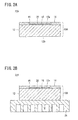
FIG. 2A is a vertical cross-sectional view showing an electronic device (first electronic device) according to the first embodiment; -
FIG. 2B is a vertical cross-sectional view showing another example of the first electronic device; -
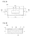
FIG. 3A is a plan view showing a first modification as viewed from an upper surface of the first heat dissipating circuit board; -
FIG. 3B is a cross-sectional view taken along line IIIB-IIIB inFIG. 3A ; -
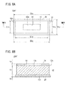
FIG. 4A is a plan view showing a second modification as viewed from an upper surface of the first heat dissipating circuit board; -
FIG. 4B is a cross-sectional view taken along line IVB-IVB inFIG. 4A ; -
FIG. 5A is a plan view showing a third modification as viewed from an upper surface of the first heat dissipating circuit board; -
FIG. 5B is a cross-sectional view taken along line VB-VB inFIG. 5A ; -
FIG. 6A is a plan view showing a fourth modification as viewed from an upper surface of the first heat dissipating circuit board; -
FIG. 6B is a cross-sectional view taken along line VIB-VIB inFIG. 6A ; -
FIG. 7A is a plan view showing a fifth modification as viewed from an upper surface of the first heat dissipating circuit board; -
FIG. 7B is a cross-sectional view taken along line VIIB-VIIB inFIG. 7A ; -
FIG. 8A is a plan view showing a sixth modification as viewed from an upper surface of the first heat dissipating circuit board; -
FIG. 8B is a cross-sectional view taken along line VIIIB-VIIIB inFIG. 8A ; -
FIG. 9A is a vertical cross-sectional view showing a seventh modification of the first heat dissipating circuit board; -
FIG. 9B is a vertical cross-sectional view showing a condition in which a heat sink is bonded to an end surface of another electrode material (second electrode material) in the seventh modification; -
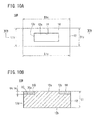
FIG. 10A is a plan view showing a heat dissipating circuit board (second heat dissipating circuit board) as viewed from an upper surface thereof according to a second embodiment of the present invention; -
FIG. 10B is a cross-sectional view taken along line XB-XB inFIG. 10A ; -
FIG. 11A is a vertical cross-sectional view showing a condition in which the depth of a recess in the second heat dissipating circuit board is shallower than the thickness of the member; -
FIG. 11B is a vertical cross-sectional view showing a condition in which the depth of a recess in the second heat dissipating circuit board is deeper than the thickness of the member; -
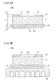
FIG. 12A is a vertical cross-sectional view showing an electronic device (second electronic device) according to the second embodiment; and -
FIG. 12B is a vertical cross-sectional view showing another second electronic device. - Below, preferred embodiments of the heat dissipating circuit board according to the present invention will be described with reference to
FIGS. 1A through 12B . In the present specification, the dash symbol "-" (or "to") shown in connection with numerical ranges implies that the numerical values appearing before and after the dash symbol include upper limit and lower limit values. - First, as shown in
FIGS. 1A and 1B , a heat dissipating circuit board (hereinafter referred to as a "first heat dissipatingcircuit board 10A") according to a first embodiment of the present invention includes anelectrode material 12 on which a power semiconductor is mounted on a front surface thereof, and a ceramic member or a semiconductor member (hereinafter referred to simply as a "member 14"), which is bonded to the front surface side of theelectrode material 12. - The
electrode material 12 can be made up from metal plates that exhibit high thermal conductivity, including Cu (copper) and Al (aluminum). Themember 14 can be made up from a ceramic that exhibits high thermal conductivity, such as AlN (aluminum nitride) or Si3N4 (silicon nitride), or alternatively, by a semiconductor such as Si (silicon), SiC (silicon carbide), or the like. Concerning the bond between theelectrode material 12 and themember 14, direct bonding, or bonding through a brazing material may be used. As a brazing material, a brazing material with an active metal added thereto, such as Ti (titanium) or the like, can be used. - In addition, in the first heat dissipating
circuit board 10A, anannular member 14 is bonded to afront surface 12a (flat surface) of theelectrode material 12. In particular, with the example ofFIGS. 1A and 1B , themember 14 is formed in an annular shape along anouter circumference 12c of thefront surface 12a of theelectrode material 12. The "front surface 12a of theelectrode material 12" is defined by a surface (e.g., the upper surface shown inFIG. 1B ) on which a power semiconductor 20 (seeFIG. 2A ) is mounted, whereas the "rear surface" thereof is defined by a surface (e.g., the lower surface shown inFIG. 1B ) opposite from thefront surface 12a. - Various shapes may be used for the shape of the
electrode material 12, although as viewed from the upper surface thereof inFIG. 1A , a rectangular shape is shown. In the center of themember 14, ahole 16 is formed, which similarly is of a rectangular shape, with thefront surface 12a of theelectrode material 12 being exposed through thehole 16. Further, the inequality t1 > ta is satisfied, where t1 represents the thickness of theelectrode material 12, and ta represents the thickness of themember 14. - Apart from the above-described rectangular shape, the outer shape of the
electrode material 12 may be a square shape, a circular shape, an elliptical shape, a track-like shape, or any of various polygonal shapes such as triangles, pentagons, hexagons, or the like. - In addition, as shown in
FIG. 2A , thepower semiconductor 20 is mounted through abonding layer 18 of solder or the like to thefront surface 12a of theelectrode material 12, whereby an electronic device (hereinafter referred to as a "firstelectronic device 22A") is made up according to the first embodiment of the invention. As shown inFIG. 2B , it is a matter of course that the firstelectronic device 22A may also be constituted by further bonding aheat sink 24 to arear surface 12b of theelectrode material 12. Moreover, as shown inFIGS. 2A and 2B , etc., although the height of thepower semiconductor 20 is illustrated as being thinner than the thickness of themember 14, the invention is not limited to this feature. - In the first heat dissipating
circuit board 10A, because themember 14 is bonded to thefront surface 12a of theelectrode material 12, thermal expansion of theelectrode material 12, which is generated during the heat cycle, and in particular, thermal expansion of a surface on which at least thepower semiconductor 20 is mounted, can be suppressed, and thermal stresses applied to thebonding layer 18 can be alleviated. In accordance therewith, generation of cracks in thebonding layer 18 can be suppressed. Further, it is possible to increase the thickness t1 of theelectrode material 12, and the thermal capacity thereof can also be increased. - Next, several modifications of the first heat dissipating
circuit board 10A will be described with reference toFIGS. 3A through 9B . - Any of the following relationships may be adopted as the relationship between the length D1y in the vertical direction and the length D1x in the horizontal (transverse) direction of the
member 14 as themember 14 is viewed from the upper surface thereof, and the length L1y in the vertical direction and the length L1x in the horizontal direction of theelectrode material 12.


- Among these relationships, the example of (A-1) is shown for the above-described first heat dissipating
circuit board 10A (seeFIGS. 1A and 1B ). - Among the aforementioned dimensional relationships, the examples of (A-2), (A-4), (A-5), (A-6), and (A-8) are illustrative of examples in which portions of the
member 14 extend out in the lateral (transverse) direction beyond theouter circumference 12c of thefront surface 12a of theelectrode material 12. The example of (A-5) (i.e., a first heat dissipating circuit board 10Aa according to a first modification) is shown representatively inFIGS. 3A and 3B . With the first modification, positional alignment when themember 14 is bonded to thefront surface 12a of theelectrode material 12 is simplified, a reduction in man-hours, an improvement in yield, and an improvement in productivity can be achieved. - The examples of (A-3), (A-7), and (A-9) are illustrative of examples in which the entirety of the
member 14 is bonded within thefront surface 12a of theelectrode material 12. The example of (A-9) (i.e., a first heat dissipating circuit board 10Ab according to a second modification) is shown representatively inFIGS. 4A and 4B . With the second modification, the constituent material amount of themember 14 can be kept to a minimum, and manufacturing costs can be reduced. - First heat dissipating circuit boards 10Ac and 10Ad according to third and fourth modifications are substantially the same in structure as the first heat dissipating
circuit board 10A, but differ therefrom in that, as shown inFIGS. 5A through 6B ,plural members 14 are arranged along theouter circumference 12c of thefront surface 12a of theelectrode material 12. With the third modification and the fourth modification, production of themembers 14 is simplified, so that a reduction in man-hours, an improvement in yield, and an improvement in productivity can be achieved. - With the third modification, as shown in
FIGS. 5A and 5B , four flat plate-shapedmembers 14 that extend in straight line shapes are arranged along theouter circumference 12c of thefront surface 12a of theelectrode material 12. With the fourth modification, as shown inFIGS. 6A and 6B , two flat plate-shapedmembers 14, which are bent in the shape of the letter L, are arranged along theouter circumference 12c of thefront surface 12a of theelectrode material 12. - As shown in
FIGS. 7A and 7B , a first heat dissipating circuit board 10Ae according to a fifth modification includes a configuration in which certain ones of themembers 14 are omitted from the aforementioned third modification. InFIGS. 7A and 7B , an example is illustrated in which two of themembers 14 having longer sides extending in the same direction are bonded (i.e., twomembers 14 that extend in straight lines are bonded at linearly symmetric positions, respectively). With the fifth modification, the constituent material amount of themember 14 can be kept to a minimum, and manufacturing costs can be reduced. - A first heat dissipating circuit board 10Af according to a sixth modification differs in that, as shown in
FIGS. 8A and 8B , aceramic substrate 26 is bonded to therear surface 12b of theelectrode material 12. - The length D2y in the vertical direction and the length D2x in the horizontal (transverse) direction as viewed from the upper surface of the
ceramic substrate 26 are longer than the length L1y in the vertical direction and the length Llx in the horizontal direction of theelectrode material 12. Theceramic substrate 26 can be made up from ceramics that exhibit high thermal conductivity, such as AlN or Si3N4. Concerning the bond between theelectrode material 12 and theceramic substrate 26, direct bonding, or bonding through a brazing material may be used. - Further, the following relationships are satisfied:


where t1 represents the thickness of theelectrode material 12, ta represents the thickness of themember 14, and tb represents the thickness of theceramic substrate 26. - In the sixth modification, the occurrence of warping can be suppressed, because the
ceramic substrate 26 also is bonded to therear surface 12b of theelectrode material 12. Further, since the thickness t1 of theelectrode material 12 can be increased, thermal resistance can effectively be reduced. - Further, as the
member 14 and theceramic substrate 26, elements preferably are used in which at least material properties and thicknesses thereof are adjusted so as to suppress warping of the first heat dissipatingcircuit board 10A. Such a feature can be accomplished by adjusting the coefficients of thermal expansion, the Young's moduli, and thereby the respective thicknesses of themember 14 and theceramic substrate 26. For example, in the case that the Young's moduli of themember 14 and theceramic substrate 26 are equal to each other, if the coefficient of thermal expansion of themember 14 is less than that of theceramic substrate 26, then the thickness of themember 14 is made thinner than theceramic substrate 26. Further, the constituent materials of themember 14 and theceramic substrate 26 may be of the same type; for example, the constituent material of themember 14 may be a ceramic. More specifically, in the case that the constituent material of theceramic substrate 26 is Si3N4, themember 14 may also be constituted from Si3N4 or the like. - A first heat dissipating circuit board 10Ag according to a seventh modification is substantially the same in structure as the aforementioned sixth modification, but differs therefrom in that, as shown in
FIG. 9A , anotherelectrode material 28 is bonded to the rear surface of theceramic substrate 26. In the seventh modification, theelectrode material 12, which is bonded to the front surface of theceramic substrate 26, is referred to as afirst electrode material 12, whereas theother electrode material 28, which is bonded to the rear surface of theceramic substrate 26, is referred to as asecond electrode material 28. - The lengths in the vertical direction and the lengths in the horizontal direction of both the
first electrode material 12 and thesecond electrode material 28 are substantially the same, respectively. - Further, the following inequality is satisfied:

where tb represents the thickness of theceramic substrate 26, t1 represents the thickness of thefirst electrode material 12, and t2 represents the thickness of thesecond electrode material 28. - In the seventh modification, similar to the aforementioned sixth modification, warping can be suppressed, and further, since the thickness t1 of the
first electrode material 12 can be increased, thermal resistance can effectively be reduced. Further, as shown inFIG. 9B , aheat sink 24 can be bonded by way of solder application or a brazing material to an end surface of thesecond electrode material 28. - Next, a heat dissipating circuit board (hereinafter referred to as a "second heat dissipating
circuit board 10B") according to a second embodiment of the present invention will be described below with reference toFIGS. 10A through 12B . - The second heat dissipating
circuit board 10B is substantially the same in structure as the above-described first heat dissipatingcircuit board 10A, but differs therefrom in that a recess 30 (seeFIG. 10B ) is included in a portion of thefront surface 12a of theelectrode material 12, and themember 14 is bonded by being embedded in therecess 30. - The
recess 30 is formed in an annular shape around theouter circumference 12c of thefront surface 12a of theelectrode material 12. In particular, with the example shown inFIGS. 10A and 10B , theouter circumference 12c of thefront surface 12a of theelectrode material 12 constitutes a portion of therecess 30. In other words, therecess 30 is formed to extend from thefront surface 12a to aside surface 12d of theelectrode material 12. Therefore, theelectrode material 12 has a shape such that a shoulder portion thereof is cut out by therecess 30. Further, themember 14 is formed in a shape along the annular shape of therecess 30. More specifically, themember 14 is bonded in an embedded fashion in therecess 30 of theelectrode material 12. Preferably, themember 14 is bonded through a brazing material or the like from abottom surface 30a of therecess 30 to aside surface 30b thereof. - As shown in
FIG. 10B , the depth tc of therecess 30 may be the same as the thickness ta of themember 14, or may be shallower than the thickness ta of themember 14 as shown inFIG. 11A . Alternatively, as shown inFIG. 11B , the depth tc of therecess 30 may be deeper than the thickness ta of themember 14. - In addition, as shown in
FIG. 12A , thepower semiconductor 20 is mounted through abonding layer 18 of solder or the like to thefront surface 12a of theelectrode material 12, whereby an electronic device (hereinafter referred to as a "secondelectronic device 22B") is made up according to the second embodiment of the invention. As shown inFIG. 12B , it is a matter of course that the secondelectronic device 22B may also be constituted by further bonding aheat sink 24 to arear surface 12b of theelectrode material 12. - In the second heat dissipating
circuit board 10B, because themember 14 is bonded to thefront surface 12a of theelectrode material 12, thermal expansion of theelectrode material 12, which is generated during the heat cycle, and in particular, thermal expansion of a surface on which at least thepower semiconductor 20 is mounted, can be suppressed, and thermal stresses applied to thebonding layer 18 can be alleviated. In accordance therewith, generation of cracks in thebonding layer 18 can be suppressed. It is possible to increase the thickness t1 of theelectrode material 12, and the thermal capacity thereof can also be increased. Further, the surface (front surface 12a of the electrode material 12) on which thepower semiconductor 20 is mounted is approximately at the same height as the surface of themember 14, or is greater in height than the surface of themember 14. Therefore, mounting of thepower semiconductor 20 can be facilitated and improved. - In the second heat dissipating
circuit board 10B, the same structures as those of the respective modifications described above for the first heat dissipatingcircuit board 10A can be adopted. - More specifically, any of the relationships (A-1) through (A-9) may be adopted as the relationship between the length D1y in the vertical direction and the length D1x in the horizontal (transverse) direction of the
member 14, and the length L1y in the vertical direction and the length Llx in the horizontal direction of theelectrode material 12. - Further, a plurality of the
members 14 may be arranged along theouter circumference 12c of thefront surface 12a of theelectrode material 12, and two of themembers 14 may be bonded such that their longer sides extend in the same direction, respectively. Aceramic substrate 26 may be bonded to therear surface 12b of theelectrode material 12, and further, theother electrode material 28 may be bonded to the rear surface of theceramic substrate 26. - An evaluation as to the presence or absence of cracks in the
bonding layer 18 was performed with respect to Inventive Examples 1 through 4 and Comparison Example 1, and an evaluation as to the presence or absence of cracks in thebonding layer 18 and theceramic substrate 26 was performed with respect to Inventive Examples 5 and 6. The results of these evaluations are shown in Table 1 and Table 2, which will be discussed below. - For the
ceramic substrate 26 and themember 14, a silicon nitride (Si3N4) board was prepared having a thickness of 0.3 mm with a bending (flexural) strength of 650 MPa. For theelectrode material 12 and theother electrode material 28, an oxygen-free copper (Cu) plate was prepared. Further, an Ag-Cu (silver/copper) type brazing material paste, to which there was added a Ti active metal powder, was prepared. - A heat dissipating circuit board for evaluation according to Example 1 included a structure similar to that of the first heat dissipating
circuit board 10A shown inFIGS. 1A and 1B . More specifically, an annular (ring-shaped)member 14 was used (denoted by the term "(annular)" in Table 1). - At first, a brazing material was coated at a thickness of 10 µm on the
member 14, and a Cu plate (electrode material 12) was bonded with themember 14. The thickness t1 of theelectrode material 12 was 2 mm. The bonding conditions were such that heated pressure bonding was carried out under a vacuum at a temperature of 800°C and a pressure of 1 MPa. Thereafter, as shown inFIG. 2A , apower semiconductor 20 was bonded through a bonding layer 18 (in this case, a solder layer) to thereby obtain an evaluation sample according to Example 1. Ten of such evaluation samples were prepared. - A heat dissipating circuit board for evaluation according to Example 2 included a structure similar to that of the first heat dissipating circuit board 10Ac according to the third modification shown in
FIGS. 5A and 5B . More specifically, fourmembers 14 were arranged and bonded along theouter circumference 12c of thefront surface 12a of the electrode material 12 (denoted by the term "(division 1)" in Table 1). Otherwise, features thereof were the same as those of Example 1, and ten of such evaluation samples according to Example 2 were prepared. - A heat dissipating circuit board for evaluation according to Example 3 included a structure similar to that of the first heat dissipating circuit board 10Ae according to the fifth modification shown in
FIGS. 7A and 7B . More specifically, twomembers 14 extending in straight line shapes were arranged and bonded at linearly symmetric positions, respectively (denoted by the term "(division 2)" in Table 1). Otherwise, features thereof were the same as those of Example 1, and ten of such evaluation samples according to Example 3 were prepared. - A heat dissipating circuit board for evaluation according to Example 4 included a structure similar to that of the second heat dissipating
circuit board 10B shown inFIGS. 10A and 10B . More specifically, an outer circumferential portion of thefront surface 12a of theelectrode material 12 was subjected to etching to thereby form anannular recess 30, and a ring-shapedmember 14 was embedded and bonded in the recess 30 (denoted by the term "(embedded)" in Table 1). Otherwise, features thereof were the same as those of Example 1, and ten of such evaluation samples according to Example 4 were prepared. - A heat dissipating circuit board for evaluation according to Example 5 included a structure similar to that of the first heat dissipating circuit board 10Af according to the sixth modification shown in
FIGS. 8A and 8B . More specifically, theceramic substrate 26 was bonded to therear surface 12b of theelectrode material 12. Otherwise, features thereof were the same as those of Example 1, and ten of such evaluation samples according to Example 5 were prepared. - A heat dissipating circuit board for evaluation according to Example 6 included a structure similar to that of the first heat dissipating circuit board 10Ag according to the seventh modification shown in
FIGS. 9A . More specifically, theceramic substrate 26 was bonded to therear surface 12b of theelectrode material 12, and further, theother electrode material 28 was bonded to the end surface of theceramic substrate 26. Otherwise, features thereof were the same as those of Example 1, and ten of such evaluation samples according to Example 6 were prepared. - A heat dissipating circuit board for evaluation according to Comparative Example 1 was the same as Inventive Example 1, except that the
member 14 was not bonded to thefront surface 12a of theelectrode material 12. Ten of such evaluation samples according to Comparative Example 1 were prepared. - First, as an evaluation method, a heat cycle test was carried out over a temperature range of -40 °C to 125 °C. The number of cycles was 100 cycles. Per each cycle, the temperature was held at -40 °C (low temperature) for 30 minutes and at 125 °C (high temperature) for 30 minutes. Upon completion of the heat cycle test, with respect to Examples 1 through 4 and Comparative Example 1, the occurrence ratio of cracks in the
bonding layer 18 was evaluated, and with respect to Examples 5 and 6, the occurrence ratio of cracks in thebonding layer 18 and the occurrence ratio of cracks in theceramic substrate 26 were evaluated. - The occurrence ratio of cracks in the
bonding layer 18 was represented by, from among ten evaluation samples, the number of evaluation samples for which cracks were generated in thebonding layer 18. The occurrence ratio of cracks in theceramic substrate 26 was represented by, from among ten evaluation samples, the number of evaluation samples for which cracks were generated in theceramic substrate 26. In Table 1 and Table 2, the ratios are expressed by [The Number of Evaluation Samples in which Cracks were Generated]/[The Evaluation Sample Parameter (= 10)]. Evaluation results for Inventive Examples 1 to 4 and Comparative Example 1 are shown in Table 1 below, whereas evaluation results for Inventive Examples 5 and 6 are shown in Table 2.[Table 1] PRESENCE OR ABSENCE OF MEMBER THICKNESS OF ELECTRODE MATERIAL OCCURRENCE RATIO OF CRACKS IN BONDING LAYER EXAMPLE 1 Present (annular) 2 mm 0/10 EXAMPLE 2 Present (division 1) 2 mm 0/10 EXAMPLE 3 Present (division 2) 2 mm 0/10 EXAMPLE 4 Present (embedded) 2 mm 0/10 COMPARATIVE EXAMPLE 1 Absent 2 mm 10/10 [Table 2] PRESENCE OR ABSENCE OF MEMBER THICKNESS OF ELECTRODE MATERIAL PRESENCE OR ABSENCE OF CERAMIC SUBSTRATE THICKNESS OF OTHER ELECTRODE MATERIAL OCCURENCE RATIO OF CRACKS IN BONDING LAYER OCCURRENCE RATIO OF CRACKS IN CERAMIC SUBSTRATE EXAMPLE 5 Present 2 mm present 0 mm 0/10 0/10 EXAMPLE 6 Present 2 mm present 0.1 mm 0/10 0/10 - From Table 1, it can be understood that, in the evaluation samples according to Examples 1 to 4, cracks were not generated in any of the bonding layers 18. This can be considered to have occurred from the fact that, because the member 14 (ceramic) was bonded to the
front surface 12a of theelectrode material 12, thermal expansion of theelectrode material 12, which is generated during the heat cycle, and in particular, thermal expansion of a surface on which at least thepower semiconductor 20 is mounted, could be suppressed, and thermal stresses applied to thebonding layer 18 were alleviated. - In contrast thereto, in Comparative Example 1, in all of the ten evaluation samples, cracks were generated in the
bonding layer 18. - On the other hand, in either of Examples 5 and 6, no cracks were generated in the
bonding layer 18 or in theceramic substrate 26. This can be considered to have occurred from the fact that, because the member 14 (ceramic) was bonded to thefront surface 12a of theelectrode material 12, similar to the case of Examples 1 through 4, thermal stresses applied to thebonding layer 18 were alleviated, and warping was suppressed due to the fact that theceramic substrate 26 was bonded to therear surface 12b of theelectrode material 12.
Claims (15)
- A heat dissipating circuit board for a power semiconductor, comprising:an electrode material (12) on which the power semiconductor (20) is mounted on a front surface (12a) thereof; anda member (14) made up from a ceramic material or a semiconductor material, which is bonded to a front surface side of the electrode material (12).
- The heat dissipating circuit board according to claim 1, wherein the member (14) is formed in an annular shape along an outer circumference (12c) of the front surface (12a) of the electrode material (12).
- The heat dissipating circuit board according to claim 1, wherein a plurality of the members (14) are provided, the plural members (14) being arranged along an outer circumference (12c) of the front surface (12a) of the electrode material (12).
- The heat dissipating circuit board according to claim 1, wherein two of the members (14) are bonded at linearly symmetric positions.
- The heat dissipating circuit board according to any one of claims 1 through 4, wherein a portion of the member (14) extends out in a transverse direction beyond an outer circumference (12c) of the front surface (12a) of the electrode material (12).
- The heat dissipating circuit board according to any one of claims 1 through 4, wherein the entirety of the member (14) is bonded within the front surface (12a) of the electrode material (12).
- The heat dissipating circuit board according to any one of claims 1 through 6, wherein:a portion of the front surface (12a) of the electrode material (12) includes a recess (30) therein; andthe member (14) is bonded in the recess (30).
- The heat dissipating circuit board according to any one of claims 1 through 7, further comprising a ceramic substrate (26), which is bonded to a rear surface (12b) of the electrode material (12).
- The heat dissipating circuit board according to claim 8, wherein at least material properties and thicknesses of the member (14) and the ceramic substrate (26) are adjusted so as to suppress warping of the heat dissipating circuit board.
- The heat dissipating circuit board according to claim 8 or 9, wherein a constituent material of the member (14) is a ceramic material, which is the same as the ceramic material of the ceramic substrate (26).
- The heat dissipating circuit board according to claim 10, wherein the constituent materials of the member (14) and the ceramic substrate (26) both are silicon nitride.
- The heat dissipating circuit board according to any one of claims 8 through 11, further comprising another electrode material (28), which is bonded to an end surface of the ceramic substrate (26).
- The heat dissipating circuit board according to claim 12, wherein the thickness of the electrode material (12) is greater than the thickness of the other electrode material (28).
- The heat dissipating circuit board according to claim 13, wherein an inequality

is satisfied, where tb represents the thickness of the ceramic substrate (26), t1 represents the thickness of the electrode material (12), and t2 represents the thickness of the other electrode material (28). - An electronic device comprising:a heat dissipating circuit board according to any one of claims 1 through 14; anda power semiconductor (20), which is mounted on the front surface (12a) of the electrode material (12) of the heat dissipating circuit board.
Applications Claiming Priority (1)
| Application Number | Priority Date | Filing Date | Title |
|---|---|---|---|
| JP2013169262 | 2013-08-16 |
Publications (2)
| Publication Number | Publication Date |
|---|---|
| EP2838327A1 true EP2838327A1 (en) | 2015-02-18 |
| EP2838327B1 EP2838327B1 (en) | 2018-11-14 |
Family
ID=50289495
Family Applications (1)
| Application Number | Title | Priority Date | Filing Date |
|---|---|---|---|
| EP14160455.3A Active EP2838327B1 (en) | 2013-08-16 | 2014-03-18 | Heat dissipating circuit board and electronic device |
Country Status (4)
| Country | Link |
|---|---|
| US (1) | US9460984B2 (en) |
| EP (1) | EP2838327B1 (en) |
| JP (1) | JPWO2015022994A1 (en) |
| WO (1) | WO2015022994A1 (en) |
Cited By (1)
| Publication number | Priority date | Publication date | Assignee | Title |
|---|---|---|---|---|
| US10748826B2 (en) | 2015-07-06 | 2020-08-18 | Rohm Co., Ltd. | Power module and inverter equipment |
Families Citing this family (4)
| Publication number | Priority date | Publication date | Assignee | Title |
|---|---|---|---|---|
| KR101956996B1 (en) * | 2016-12-15 | 2019-06-24 | 현대자동차주식회사 | Power module of double-side cooling |
| KR20200131293A (en) | 2018-03-19 | 2020-11-23 | 가부시키가이샤 리코 | Photoelectric conversion device, process cartridge and image forming apparatus |
| KR102574378B1 (en) | 2018-10-04 | 2023-09-04 | 현대자동차주식회사 | Power module |
| KR102671539B1 (en) * | 2019-04-26 | 2024-05-31 | 덴카 주식회사 | Electronic component modules, and silicon nitride circuit boards |
Citations (6)
| Publication number | Priority date | Publication date | Assignee | Title |
|---|---|---|---|---|
| US5731067A (en) * | 1995-06-07 | 1998-03-24 | Denso Corporation | Multi-layered substrate |
| EP0874399A1 (en) * | 1996-08-20 | 1998-10-28 | Kabushiki Kaisha Toshiba | Silicon nitride circuit board and semiconductor module |
| JP2003086747A (en) * | 2001-09-10 | 2003-03-20 | Hitachi Ltd | Insulated circuit board, method of manufacturing the same, and semiconductor power device using the same |
| JP2008153430A (en) | 2006-12-18 | 2008-07-03 | Mitsubishi Electric Corp | Heat dissipation board, heat conductive sheet and power module using them |
| US20130094165A1 (en) * | 2011-10-12 | 2013-04-18 | Ngk Insulators, Ltd. | High-capacity module including the peripheral circuit using the circuit board and the circuit board concerned for peripheral circuits of a high-capacity module |
| WO2014095587A1 (en) * | 2012-12-21 | 2014-06-26 | Epcos Ag | Component carrier and component carrier arrangement |
Family Cites Families (11)
| Publication number | Priority date | Publication date | Assignee | Title |
|---|---|---|---|---|
| US7329563B2 (en) * | 2002-09-03 | 2008-02-12 | Industrial Technology Research Institute | Method for fabrication of wafer level package incorporating dual compliant layers |
| JP2004327732A (en) * | 2003-04-24 | 2004-11-18 | Kyocera Corp | Ceramic circuit board and electric circuit module |
| JP4377617B2 (en) * | 2003-06-20 | 2009-12-02 | 日本特殊陶業株式会社 | Capacitor, semiconductor element with capacitor, wiring board with capacitor, and electronic unit including semiconductor element, capacitor, and wiring board |
| JP2006041256A (en) * | 2004-07-28 | 2006-02-09 | Nissan Motor Co Ltd | Semiconductor device and manufacturing method thereof |
| JP2006294890A (en) * | 2005-04-12 | 2006-10-26 | Nissan Motor Co Ltd | Semiconductor device and manufacturing method thereof |
| JP4760267B2 (en) * | 2005-09-28 | 2011-08-31 | 日産自動車株式会社 | Junction structure |
| JP2009117701A (en) * | 2007-11-08 | 2009-05-28 | Toyota Motor Corp | Power module |
| EP2549535B1 (en) * | 2010-03-19 | 2015-11-04 | Panasonic Intellectual Property Management Co., Ltd. | Nonvolatile memory element and production method therefor |
| JP5699442B2 (en) * | 2010-04-07 | 2015-04-08 | 三菱マテリアル株式会社 | Power module substrate and power module |
| JP2012074591A (en) * | 2010-09-29 | 2012-04-12 | Kyocera Corp | Circuit board and electronic divice |
| JP6095303B2 (en) * | 2012-09-07 | 2017-03-15 | 三菱電機株式会社 | Semiconductor device and manufacturing method of semiconductor device |
-
2014
- 2014-03-18 EP EP14160455.3A patent/EP2838327B1/en active Active
- 2014-08-15 JP JP2015531838A patent/JPWO2015022994A1/en active Pending
- 2014-08-15 WO PCT/JP2014/071481 patent/WO2015022994A1/en not_active Ceased
-
2016
- 2016-02-11 US US15/041,167 patent/US9460984B2/en active Active
Patent Citations (6)
| Publication number | Priority date | Publication date | Assignee | Title |
|---|---|---|---|---|
| US5731067A (en) * | 1995-06-07 | 1998-03-24 | Denso Corporation | Multi-layered substrate |
| EP0874399A1 (en) * | 1996-08-20 | 1998-10-28 | Kabushiki Kaisha Toshiba | Silicon nitride circuit board and semiconductor module |
| JP2003086747A (en) * | 2001-09-10 | 2003-03-20 | Hitachi Ltd | Insulated circuit board, method of manufacturing the same, and semiconductor power device using the same |
| JP2008153430A (en) | 2006-12-18 | 2008-07-03 | Mitsubishi Electric Corp | Heat dissipation board, heat conductive sheet and power module using them |
| US20130094165A1 (en) * | 2011-10-12 | 2013-04-18 | Ngk Insulators, Ltd. | High-capacity module including the peripheral circuit using the circuit board and the circuit board concerned for peripheral circuits of a high-capacity module |
| WO2014095587A1 (en) * | 2012-12-21 | 2014-06-26 | Epcos Ag | Component carrier and component carrier arrangement |
Cited By (1)
| Publication number | Priority date | Publication date | Assignee | Title |
|---|---|---|---|---|
| US10748826B2 (en) | 2015-07-06 | 2020-08-18 | Rohm Co., Ltd. | Power module and inverter equipment |
Also Published As
| Publication number | Publication date |
|---|---|
| US20160163618A1 (en) | 2016-06-09 |
| JPWO2015022994A1 (en) | 2017-03-02 |
| US9460984B2 (en) | 2016-10-04 |
| WO2015022994A1 (en) | 2015-02-19 |
| EP2838327B1 (en) | 2018-11-14 |
Similar Documents
| Publication | Publication Date | Title |
|---|---|---|
| EP2838325B1 (en) | Ceramic circuit board and electronic device | |
| US10068829B2 (en) | Power-module substrate unit and power module | |
| EP2259308B1 (en) | Substrate for power module with heat sink and method for producing the same, power module with heat sink, and substrate for power module | |
| US8564118B2 (en) | Power module substrate, power module, and method for manufacturing power module substrate | |
| JP5598522B2 (en) | Circuit board, semiconductor module using the same, and circuit board manufacturing method | |
| US10453772B2 (en) | Heat-sink-attached power-module substrate and power module | |
| US6844621B2 (en) | Semiconductor device and method of relaxing thermal stress | |
| US8198540B2 (en) | Power element mounting substrate, method of manufacturing the same, power element mounting unit, method of manufacturing the same, and power module | |
| EP2838327B1 (en) | Heat dissipating circuit board and electronic device | |
| EP2838326B1 (en) | Electronic device | |
| KR102636824B1 (en) | Carrier substrates and methods for manufacturing carrier substrates for electrical, especially electronic, components | |
| CN107004643A (en) | Circuit boards and electronic devices | |
| JP4124040B2 (en) | Semiconductor device | |
| JP5772088B2 (en) | Power module substrate manufacturing method and power module substrate | |
| JP5614127B2 (en) | Power module substrate and manufacturing method thereof | |
| JP4656126B2 (en) | Semiconductor device | |
| JP2001135789A (en) | Multilayer ceramic substrate and power module substrate using the same | |
| JP2018006377A (en) | Composite substrate, electronic device, and electronic module | |
| KR20130042777A (en) | Fabrication method of clad metal for high heat realease | |
| JP2013021115A (en) | Ceramic circuit board and electronic apparatus using the same | |
| JP2011054853A (en) | Silicon nitride substrate improved in positioning property, and semiconductor device using the same |
Legal Events
| Date | Code | Title | Description |
|---|---|---|---|
| 17P | Request for examination filed |
Effective date: 20140318 |
|
| AK | Designated contracting states |
Kind code of ref document: A1 Designated state(s): AL AT BE BG CH CY CZ DE DK EE ES FI FR GB GR HR HU IE IS IT LI LT LU LV MC MK MT NL NO PL PT RO RS SE SI SK SM TR |
|
| AX | Request for extension of the european patent |
Extension state: BA ME |
|
| PUAI | Public reference made under article 153(3) epc to a published international application that has entered the european phase |
Free format text: ORIGINAL CODE: 0009012 |
|
| R17P | Request for examination filed (corrected) |
Effective date: 20150817 |
|
| RBV | Designated contracting states (corrected) |
Designated state(s): AL AT BE BG CH CY CZ DE DK EE ES FI FR GB GR HR HU IE IS IT LI LT LU LV MC MK MT NL NO PL PT RO RS SE SI SK SM TR |
|
| GRAP | Despatch of communication of intention to grant a patent |
Free format text: ORIGINAL CODE: EPIDOSNIGR1 |
|
| STAA | Information on the status of an ep patent application or granted ep patent |
Free format text: STATUS: GRANT OF PATENT IS INTENDED |
|
| INTG | Intention to grant announced |
Effective date: 20180528 |
|
| GRAS | Grant fee paid |
Free format text: ORIGINAL CODE: EPIDOSNIGR3 |
|
| GRAA | (expected) grant |
Free format text: ORIGINAL CODE: 0009210 |
|
| STAA | Information on the status of an ep patent application or granted ep patent |
Free format text: STATUS: THE PATENT HAS BEEN GRANTED |
|
| AK | Designated contracting states |
Kind code of ref document: B1 Designated state(s): AL AT BE BG CH CY CZ DE DK EE ES FI FR GB GR HR HU IE IS IT LI LT LU LV MC MK MT NL NO PL PT RO RS SE SI SK SM TR |
|
| REG | Reference to a national code |
Ref country code: CH Ref legal event code: EP Ref country code: AT Ref legal event code: REF Ref document number: 1066391 Country of ref document: AT Kind code of ref document: T Effective date: 20181115 |
|
| REG | Reference to a national code |
Ref country code: DE Ref legal event code: R096 Ref document number: 602014035866 Country of ref document: DE |
|
| REG | Reference to a national code |
Ref country code: IE Ref legal event code: FG4D |
|
| REG | Reference to a national code |
Ref country code: NL Ref legal event code: MP Effective date: 20181114 |
|
| REG | Reference to a national code |
Ref country code: LT Ref legal event code: MG4D |
|
| REG | Reference to a national code |
Ref country code: AT Ref legal event code: MK05 Ref document number: 1066391 Country of ref document: AT Kind code of ref document: T Effective date: 20181114 |
|
| PG25 | Lapsed in a contracting state [announced via postgrant information from national office to epo] |
Ref country code: IS Free format text: LAPSE BECAUSE OF FAILURE TO SUBMIT A TRANSLATION OF THE DESCRIPTION OR TO PAY THE FEE WITHIN THE PRESCRIBED TIME-LIMIT Effective date: 20190314 Ref country code: FI Free format text: LAPSE BECAUSE OF FAILURE TO SUBMIT A TRANSLATION OF THE DESCRIPTION OR TO PAY THE FEE WITHIN THE PRESCRIBED TIME-LIMIT Effective date: 20181114 Ref country code: LV Free format text: LAPSE BECAUSE OF FAILURE TO SUBMIT A TRANSLATION OF THE DESCRIPTION OR TO PAY THE FEE WITHIN THE PRESCRIBED TIME-LIMIT Effective date: 20181114 Ref country code: AT Free format text: LAPSE BECAUSE OF FAILURE TO SUBMIT A TRANSLATION OF THE DESCRIPTION OR TO PAY THE FEE WITHIN THE PRESCRIBED TIME-LIMIT Effective date: 20181114 Ref country code: HR Free format text: LAPSE BECAUSE OF FAILURE TO SUBMIT A TRANSLATION OF THE DESCRIPTION OR TO PAY THE FEE WITHIN THE PRESCRIBED TIME-LIMIT Effective date: 20181114 Ref country code: BG Free format text: LAPSE BECAUSE OF FAILURE TO SUBMIT A TRANSLATION OF THE DESCRIPTION OR TO PAY THE FEE WITHIN THE PRESCRIBED TIME-LIMIT Effective date: 20190214 Ref country code: NO Free format text: LAPSE BECAUSE OF FAILURE TO SUBMIT A TRANSLATION OF THE DESCRIPTION OR TO PAY THE FEE WITHIN THE PRESCRIBED TIME-LIMIT Effective date: 20190214 Ref country code: LT Free format text: LAPSE BECAUSE OF FAILURE TO SUBMIT A TRANSLATION OF THE DESCRIPTION OR TO PAY THE FEE WITHIN THE PRESCRIBED TIME-LIMIT Effective date: 20181114 Ref country code: ES Free format text: LAPSE BECAUSE OF FAILURE TO SUBMIT A TRANSLATION OF THE DESCRIPTION OR TO PAY THE FEE WITHIN THE PRESCRIBED TIME-LIMIT Effective date: 20181114 |
|
| PG25 | Lapsed in a contracting state [announced via postgrant information from national office to epo] |
Ref country code: AL Free format text: LAPSE BECAUSE OF FAILURE TO SUBMIT A TRANSLATION OF THE DESCRIPTION OR TO PAY THE FEE WITHIN THE PRESCRIBED TIME-LIMIT Effective date: 20181114 Ref country code: PT Free format text: LAPSE BECAUSE OF FAILURE TO SUBMIT A TRANSLATION OF THE DESCRIPTION OR TO PAY THE FEE WITHIN THE PRESCRIBED TIME-LIMIT Effective date: 20190314 Ref country code: NL Free format text: LAPSE BECAUSE OF FAILURE TO SUBMIT A TRANSLATION OF THE DESCRIPTION OR TO PAY THE FEE WITHIN THE PRESCRIBED TIME-LIMIT Effective date: 20181114 Ref country code: GR Free format text: LAPSE BECAUSE OF FAILURE TO SUBMIT A TRANSLATION OF THE DESCRIPTION OR TO PAY THE FEE WITHIN THE PRESCRIBED TIME-LIMIT Effective date: 20190215 Ref country code: SE Free format text: LAPSE BECAUSE OF FAILURE TO SUBMIT A TRANSLATION OF THE DESCRIPTION OR TO PAY THE FEE WITHIN THE PRESCRIBED TIME-LIMIT Effective date: 20181114 Ref country code: RS Free format text: LAPSE BECAUSE OF FAILURE TO SUBMIT A TRANSLATION OF THE DESCRIPTION OR TO PAY THE FEE WITHIN THE PRESCRIBED TIME-LIMIT Effective date: 20181114 |
|
| PG25 | Lapsed in a contracting state [announced via postgrant information from national office to epo] |
Ref country code: CZ Free format text: LAPSE BECAUSE OF FAILURE TO SUBMIT A TRANSLATION OF THE DESCRIPTION OR TO PAY THE FEE WITHIN THE PRESCRIBED TIME-LIMIT Effective date: 20181114 Ref country code: IT Free format text: LAPSE BECAUSE OF FAILURE TO SUBMIT A TRANSLATION OF THE DESCRIPTION OR TO PAY THE FEE WITHIN THE PRESCRIBED TIME-LIMIT Effective date: 20181114 Ref country code: DK Free format text: LAPSE BECAUSE OF FAILURE TO SUBMIT A TRANSLATION OF THE DESCRIPTION OR TO PAY THE FEE WITHIN THE PRESCRIBED TIME-LIMIT Effective date: 20181114 Ref country code: PL Free format text: LAPSE BECAUSE OF FAILURE TO SUBMIT A TRANSLATION OF THE DESCRIPTION OR TO PAY THE FEE WITHIN THE PRESCRIBED TIME-LIMIT Effective date: 20181114 |
|
| REG | Reference to a national code |
Ref country code: DE Ref legal event code: R097 Ref document number: 602014035866 Country of ref document: DE |
|
| PG25 | Lapsed in a contracting state [announced via postgrant information from national office to epo] |
Ref country code: EE Free format text: LAPSE BECAUSE OF FAILURE TO SUBMIT A TRANSLATION OF THE DESCRIPTION OR TO PAY THE FEE WITHIN THE PRESCRIBED TIME-LIMIT Effective date: 20181114 Ref country code: SM Free format text: LAPSE BECAUSE OF FAILURE TO SUBMIT A TRANSLATION OF THE DESCRIPTION OR TO PAY THE FEE WITHIN THE PRESCRIBED TIME-LIMIT Effective date: 20181114 Ref country code: RO Free format text: LAPSE BECAUSE OF FAILURE TO SUBMIT A TRANSLATION OF THE DESCRIPTION OR TO PAY THE FEE WITHIN THE PRESCRIBED TIME-LIMIT Effective date: 20181114 Ref country code: SK Free format text: LAPSE BECAUSE OF FAILURE TO SUBMIT A TRANSLATION OF THE DESCRIPTION OR TO PAY THE FEE WITHIN THE PRESCRIBED TIME-LIMIT Effective date: 20181114 |
|
| PLBE | No opposition filed within time limit |
Free format text: ORIGINAL CODE: 0009261 |
|
| STAA | Information on the status of an ep patent application or granted ep patent |
Free format text: STATUS: NO OPPOSITION FILED WITHIN TIME LIMIT |
|
| 26N | No opposition filed |
Effective date: 20190815 |
|
| PG25 | Lapsed in a contracting state [announced via postgrant information from national office to epo] |
Ref country code: MC Free format text: LAPSE BECAUSE OF FAILURE TO SUBMIT A TRANSLATION OF THE DESCRIPTION OR TO PAY THE FEE WITHIN THE PRESCRIBED TIME-LIMIT Effective date: 20181114 Ref country code: SI Free format text: LAPSE BECAUSE OF FAILURE TO SUBMIT A TRANSLATION OF THE DESCRIPTION OR TO PAY THE FEE WITHIN THE PRESCRIBED TIME-LIMIT Effective date: 20181114 |
|
| REG | Reference to a national code |
Ref country code: CH Ref legal event code: PL |
|
| PG25 | Lapsed in a contracting state [announced via postgrant information from national office to epo] |
Ref country code: LU Free format text: LAPSE BECAUSE OF NON-PAYMENT OF DUE FEES Effective date: 20190318 |
|
| REG | Reference to a national code |
Ref country code: BE Ref legal event code: MM Effective date: 20190331 |
|
| PG25 | Lapsed in a contracting state [announced via postgrant information from national office to epo] |
Ref country code: IE Free format text: LAPSE BECAUSE OF NON-PAYMENT OF DUE FEES Effective date: 20190318 Ref country code: LI Free format text: LAPSE BECAUSE OF NON-PAYMENT OF DUE FEES Effective date: 20190331 Ref country code: CH Free format text: LAPSE BECAUSE OF NON-PAYMENT OF DUE FEES Effective date: 20190331 |
|
| PG25 | Lapsed in a contracting state [announced via postgrant information from national office to epo] |
Ref country code: BE Free format text: LAPSE BECAUSE OF NON-PAYMENT OF DUE FEES Effective date: 20190331 |
|
| PG25 | Lapsed in a contracting state [announced via postgrant information from national office to epo] |
Ref country code: TR Free format text: LAPSE BECAUSE OF FAILURE TO SUBMIT A TRANSLATION OF THE DESCRIPTION OR TO PAY THE FEE WITHIN THE PRESCRIBED TIME-LIMIT Effective date: 20181114 |
|
| PG25 | Lapsed in a contracting state [announced via postgrant information from national office to epo] |
Ref country code: MT Free format text: LAPSE BECAUSE OF NON-PAYMENT OF DUE FEES Effective date: 20190318 |
|
| PG25 | Lapsed in a contracting state [announced via postgrant information from national office to epo] |
Ref country code: CY Free format text: LAPSE BECAUSE OF FAILURE TO SUBMIT A TRANSLATION OF THE DESCRIPTION OR TO PAY THE FEE WITHIN THE PRESCRIBED TIME-LIMIT Effective date: 20181114 |
|
| PG25 | Lapsed in a contracting state [announced via postgrant information from national office to epo] |
Ref country code: HU Free format text: LAPSE BECAUSE OF FAILURE TO SUBMIT A TRANSLATION OF THE DESCRIPTION OR TO PAY THE FEE WITHIN THE PRESCRIBED TIME-LIMIT; INVALID AB INITIO Effective date: 20140318 |
|
| PG25 | Lapsed in a contracting state [announced via postgrant information from national office to epo] |
Ref country code: MK Free format text: LAPSE BECAUSE OF FAILURE TO SUBMIT A TRANSLATION OF THE DESCRIPTION OR TO PAY THE FEE WITHIN THE PRESCRIBED TIME-LIMIT Effective date: 20181114 |
|
| PGFP | Annual fee paid to national office [announced via postgrant information from national office to epo] |
Ref country code: DE Payment date: 20250128 Year of fee payment: 12 |
|
| PGFP | Annual fee paid to national office [announced via postgrant information from national office to epo] |
Ref country code: FR Payment date: 20250210 Year of fee payment: 12 |
|
| PGFP | Annual fee paid to national office [announced via postgrant information from national office to epo] |
Ref country code: GB Payment date: 20250130 Year of fee payment: 12 |