EP2835825A1 - SOI integrated circuit provided with a device for protection against electrostatic discharges - Google Patents
SOI integrated circuit provided with a device for protection against electrostatic discharges Download PDFInfo
- Publication number
- EP2835825A1 EP2835825A1 EP14178657.4A EP14178657A EP2835825A1 EP 2835825 A1 EP2835825 A1 EP 2835825A1 EP 14178657 A EP14178657 A EP 14178657A EP 2835825 A1 EP2835825 A1 EP 2835825A1
- Authority
- EP
- European Patent Office
- Prior art keywords
- base
- transistor
- doping
- insulating layer
- ground plane
- Prior art date
- Legal status (The legal status is an assumption and is not a legal conclusion. Google has not performed a legal analysis and makes no representation as to the accuracy of the status listed.)
- Withdrawn
Links
- 239000004065 semiconductor Substances 0.000 claims abstract description 81
- 238000002513 implantation Methods 0.000 claims description 54
- 239000000758 substrate Substances 0.000 claims description 27
- 238000004519 manufacturing process Methods 0.000 claims description 18
- 230000015572 biosynthetic process Effects 0.000 claims description 13
- 239000012212 insulator Substances 0.000 claims description 6
- 238000000034 method Methods 0.000 claims description 6
- 238000002955 isolation Methods 0.000 description 54
- 229910052751 metal Inorganic materials 0.000 description 32
- 239000002184 metal Substances 0.000 description 32
- 230000010287 polarization Effects 0.000 description 24
- 238000009413 insulation Methods 0.000 description 15
- XUIMIQQOPSSXEZ-UHFFFAOYSA-N Silicon Chemical compound [Si] XUIMIQQOPSSXEZ-UHFFFAOYSA-N 0.000 description 10
- 238000010586 diagram Methods 0.000 description 10
- 229910052710 silicon Inorganic materials 0.000 description 10
- 239000010703 silicon Substances 0.000 description 10
- 238000000407 epitaxy Methods 0.000 description 8
- 150000004767 nitrides Chemical class 0.000 description 8
- 230000001681 protective effect Effects 0.000 description 7
- 238000005516 engineering process Methods 0.000 description 6
- 230000001965 increasing effect Effects 0.000 description 6
- 238000000206 photolithography Methods 0.000 description 5
- 238000011084 recovery Methods 0.000 description 5
- 239000002019 doping agent Substances 0.000 description 4
- 239000000463 material Substances 0.000 description 3
- 238000005259 measurement Methods 0.000 description 3
- VYPSYNLAJGMNEJ-UHFFFAOYSA-N Silicium dioxide Chemical compound O=[Si]=O VYPSYNLAJGMNEJ-UHFFFAOYSA-N 0.000 description 2
- 238000007667 floating Methods 0.000 description 2
- 230000010354 integration Effects 0.000 description 2
- 230000003071 parasitic effect Effects 0.000 description 2
- 229910052814 silicon oxide Inorganic materials 0.000 description 2
- 240000008042 Zea mays Species 0.000 description 1
- 238000000137 annealing Methods 0.000 description 1
- 229910052785 arsenic Inorganic materials 0.000 description 1
- RQNWIZPPADIBDY-UHFFFAOYSA-N arsenic atom Chemical compound [As] RQNWIZPPADIBDY-UHFFFAOYSA-N 0.000 description 1
- 230000002457 bidirectional effect Effects 0.000 description 1
- 239000000969 carrier Substances 0.000 description 1
- 230000015556 catabolic process Effects 0.000 description 1
- 230000000694 effects Effects 0.000 description 1
- 238000010292 electrical insulation Methods 0.000 description 1
- 230000006870 function Effects 0.000 description 1
- 229910052738 indium Inorganic materials 0.000 description 1
- APFVFJFRJDLVQX-UHFFFAOYSA-N indium atom Chemical compound [In] APFVFJFRJDLVQX-UHFFFAOYSA-N 0.000 description 1
- 230000001939 inductive effect Effects 0.000 description 1
- 230000005865 ionizing radiation Effects 0.000 description 1
- 238000005457 optimization Methods 0.000 description 1
- 230000005855 radiation Effects 0.000 description 1
- 238000004513 sizing Methods 0.000 description 1
- 230000001960 triggered effect Effects 0.000 description 1
Images


Classifications
-
- H—ELECTRICITY
- H01—ELECTRIC ELEMENTS
- H01L—SEMICONDUCTOR DEVICES NOT COVERED BY CLASS H10
- H01L27/00—Devices consisting of a plurality of semiconductor or other solid-state components formed in or on a common substrate
- H01L27/02—Devices consisting of a plurality of semiconductor or other solid-state components formed in or on a common substrate including semiconductor components specially adapted for rectifying, oscillating, amplifying or switching and having at least one potential-jump barrier or surface barrier; including integrated passive circuit elements with at least one potential-jump barrier or surface barrier
- H01L27/0203—Particular design considerations for integrated circuits
- H01L27/0248—Particular design considerations for integrated circuits for electrical or thermal protection, e.g. electrostatic discharge [ESD] protection
- H01L27/0251—Particular design considerations for integrated circuits for electrical or thermal protection, e.g. electrostatic discharge [ESD] protection for MOS devices
- H01L27/0259—Particular design considerations for integrated circuits for electrical or thermal protection, e.g. electrostatic discharge [ESD] protection for MOS devices using bipolar transistors as protective elements
- H01L27/0262—Particular design considerations for integrated circuits for electrical or thermal protection, e.g. electrostatic discharge [ESD] protection for MOS devices using bipolar transistors as protective elements including a PNP transistor and a NPN transistor, wherein each of said transistors has its base coupled to the collector of the other transistor, e.g. silicon controlled rectifier [SCR] devices
-
- H—ELECTRICITY
- H01—ELECTRIC ELEMENTS
- H01L—SEMICONDUCTOR DEVICES NOT COVERED BY CLASS H10
- H01L27/00—Devices consisting of a plurality of semiconductor or other solid-state components formed in or on a common substrate
- H01L27/02—Devices consisting of a plurality of semiconductor or other solid-state components formed in or on a common substrate including semiconductor components specially adapted for rectifying, oscillating, amplifying or switching and having at least one potential-jump barrier or surface barrier; including integrated passive circuit elements with at least one potential-jump barrier or surface barrier
- H01L27/12—Devices consisting of a plurality of semiconductor or other solid-state components formed in or on a common substrate including semiconductor components specially adapted for rectifying, oscillating, amplifying or switching and having at least one potential-jump barrier or surface barrier; including integrated passive circuit elements with at least one potential-jump barrier or surface barrier the substrate being other than a semiconductor body, e.g. an insulating body
- H01L27/1203—Devices consisting of a plurality of semiconductor or other solid-state components formed in or on a common substrate including semiconductor components specially adapted for rectifying, oscillating, amplifying or switching and having at least one potential-jump barrier or surface barrier; including integrated passive circuit elements with at least one potential-jump barrier or surface barrier the substrate being other than a semiconductor body, e.g. an insulating body the substrate comprising an insulating body on a semiconductor body, e.g. SOI
-
- H—ELECTRICITY
- H01—ELECTRIC ELEMENTS
- H01L—SEMICONDUCTOR DEVICES NOT COVERED BY CLASS H10
- H01L29/00—Semiconductor devices adapted for rectifying, amplifying, oscillating or switching, or capacitors or resistors with at least one potential-jump barrier or surface barrier, e.g. PN junction depletion layer or carrier concentration layer; Details of semiconductor bodies or of electrodes thereof ; Multistep manufacturing processes therefor
- H01L29/02—Semiconductor bodies ; Multistep manufacturing processes therefor
- H01L29/06—Semiconductor bodies ; Multistep manufacturing processes therefor characterised by their shape; characterised by the shapes, relative sizes, or dispositions of the semiconductor regions ; characterised by the concentration or distribution of impurities within semiconductor regions
- H01L29/10—Semiconductor bodies ; Multistep manufacturing processes therefor characterised by their shape; characterised by the shapes, relative sizes, or dispositions of the semiconductor regions ; characterised by the concentration or distribution of impurities within semiconductor regions with semiconductor regions connected to an electrode not carrying current to be rectified, amplified or switched and such electrode being part of a semiconductor device which comprises three or more electrodes
- H01L29/1012—Base regions of thyristors
-
- H—ELECTRICITY
- H01—ELECTRIC ELEMENTS
- H01L—SEMICONDUCTOR DEVICES NOT COVERED BY CLASS H10
- H01L29/00—Semiconductor devices adapted for rectifying, amplifying, oscillating or switching, or capacitors or resistors with at least one potential-jump barrier or surface barrier, e.g. PN junction depletion layer or carrier concentration layer; Details of semiconductor bodies or of electrodes thereof ; Multistep manufacturing processes therefor
- H01L29/40—Electrodes ; Multistep manufacturing processes therefor
- H01L29/41—Electrodes ; Multistep manufacturing processes therefor characterised by their shape, relative sizes or dispositions
- H01L29/423—Electrodes ; Multistep manufacturing processes therefor characterised by their shape, relative sizes or dispositions not carrying the current to be rectified, amplified or switched
- H01L29/42308—Gate electrodes for thyristors
-
- H—ELECTRICITY
- H01—ELECTRIC ELEMENTS
- H01L—SEMICONDUCTOR DEVICES NOT COVERED BY CLASS H10
- H01L29/00—Semiconductor devices adapted for rectifying, amplifying, oscillating or switching, or capacitors or resistors with at least one potential-jump barrier or surface barrier, e.g. PN junction depletion layer or carrier concentration layer; Details of semiconductor bodies or of electrodes thereof ; Multistep manufacturing processes therefor
- H01L29/66—Types of semiconductor device ; Multistep manufacturing processes therefor
- H01L29/66007—Multistep manufacturing processes
- H01L29/66075—Multistep manufacturing processes of devices having semiconductor bodies comprising group 14 or group 13/15 materials
- H01L29/66227—Multistep manufacturing processes of devices having semiconductor bodies comprising group 14 or group 13/15 materials the devices being controllable only by the electric current supplied or the electric potential applied, to an electrode which does not carry the current to be rectified, amplified or switched, e.g. three-terminal devices
- H01L29/66409—Unipolar field-effect transistors
- H01L29/66477—Unipolar field-effect transistors with an insulated gate, i.e. MISFET
-
- H—ELECTRICITY
- H01—ELECTRIC ELEMENTS
- H01L—SEMICONDUCTOR DEVICES NOT COVERED BY CLASS H10
- H01L29/00—Semiconductor devices adapted for rectifying, amplifying, oscillating or switching, or capacitors or resistors with at least one potential-jump barrier or surface barrier, e.g. PN junction depletion layer or carrier concentration layer; Details of semiconductor bodies or of electrodes thereof ; Multistep manufacturing processes therefor
- H01L29/66—Types of semiconductor device ; Multistep manufacturing processes therefor
- H01L29/68—Types of semiconductor device ; Multistep manufacturing processes therefor controllable by only the electric current supplied, or only the electric potential applied, to an electrode which does not carry the current to be rectified, amplified or switched
- H01L29/70—Bipolar devices
- H01L29/74—Thyristor-type devices, e.g. having four-zone regenerative action
- H01L29/7436—Lateral thyristors
-
- H—ELECTRICITY
- H01—ELECTRIC ELEMENTS
- H01L—SEMICONDUCTOR DEVICES NOT COVERED BY CLASS H10
- H01L29/00—Semiconductor devices adapted for rectifying, amplifying, oscillating or switching, or capacitors or resistors with at least one potential-jump barrier or surface barrier, e.g. PN junction depletion layer or carrier concentration layer; Details of semiconductor bodies or of electrodes thereof ; Multistep manufacturing processes therefor
- H01L29/66—Types of semiconductor device ; Multistep manufacturing processes therefor
- H01L29/68—Types of semiconductor device ; Multistep manufacturing processes therefor controllable by only the electric current supplied, or only the electric potential applied, to an electrode which does not carry the current to be rectified, amplified or switched
- H01L29/70—Bipolar devices
- H01L29/74—Thyristor-type devices, e.g. having four-zone regenerative action
- H01L29/747—Bidirectional devices, e.g. triacs
-
- H—ELECTRICITY
- H01—ELECTRIC ELEMENTS
- H01L—SEMICONDUCTOR DEVICES NOT COVERED BY CLASS H10
- H01L29/00—Semiconductor devices adapted for rectifying, amplifying, oscillating or switching, or capacitors or resistors with at least one potential-jump barrier or surface barrier, e.g. PN junction depletion layer or carrier concentration layer; Details of semiconductor bodies or of electrodes thereof ; Multistep manufacturing processes therefor
- H01L29/66—Types of semiconductor device ; Multistep manufacturing processes therefor
- H01L29/68—Types of semiconductor device ; Multistep manufacturing processes therefor controllable by only the electric current supplied, or only the electric potential applied, to an electrode which does not carry the current to be rectified, amplified or switched
- H01L29/70—Bipolar devices
- H01L29/74—Thyristor-type devices, e.g. having four-zone regenerative action
- H01L29/749—Thyristor-type devices, e.g. having four-zone regenerative action with turn-on by field effect
-
- H—ELECTRICITY
- H01—ELECTRIC ELEMENTS
- H01L—SEMICONDUCTOR DEVICES NOT COVERED BY CLASS H10
- H01L29/00—Semiconductor devices adapted for rectifying, amplifying, oscillating or switching, or capacitors or resistors with at least one potential-jump barrier or surface barrier, e.g. PN junction depletion layer or carrier concentration layer; Details of semiconductor bodies or of electrodes thereof ; Multistep manufacturing processes therefor
- H01L29/66—Types of semiconductor device ; Multistep manufacturing processes therefor
- H01L29/68—Types of semiconductor device ; Multistep manufacturing processes therefor controllable by only the electric current supplied, or only the electric potential applied, to an electrode which does not carry the current to be rectified, amplified or switched
- H01L29/76—Unipolar devices, e.g. field effect transistors
- H01L29/772—Field effect transistors
- H01L29/78—Field effect transistors with field effect produced by an insulated gate
- H01L29/7833—Field effect transistors with field effect produced by an insulated gate with lightly doped drain or source extension, e.g. LDD MOSFET's; DDD MOSFET's
Definitions
- the invention relates to integrated circuits, and in particular integrated circuits made on a silicon-on-insulator (SOI) type substrate.
- SOI technology consists of separating a thin layer of silicon (a few nanometers) on a silicon substrate by a relatively thick insulating layer (a few tens of nanometers as a rule).
- Integrated circuits made in SOI technology have a number of advantages. Such circuits generally have lower power consumption for equivalent performance. Such circuits also induce lower parasitic capacitances, which make it possible to improve the switching speed. In addition, the phenomenon of latchup in the English language encountered by MOS transistors Bulk technology can be avoided. Such circuits are therefore particularly suitable for SoC or MEMS type applications. It can also be seen that the SOI integrated circuits are less sensitive to the effects of ionizing radiation and thus prove more reliable in applications where such radiations can induce operating problems, especially in space applications.
- the SOI integrated circuits can notably comprise SRAM-type random access devices or logic gates.
- Such integrated circuits also include protection devices against electrostatic discharges (ESD for "Electrostatic Discharge” in English) accidental and can deteriorate these transistors.
- ESD electrostatic Discharge
- the design of an ESD device is performed to meet a number of technological constraints.
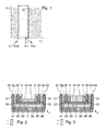
- the figure 1 is an example of a voltage / current diagram of an ESD device during a discharge.
- Vt1 When an electrostatic discharge occurs, the voltage across the ESD device first increases to a trigger voltage Vt1.
- the current flowing through the ESD device also grows slightly (low leakage).
- This voltage Vt1 must remain below a voltage Vm, corresponding to a breakdown voltage in MOS technology, typically 2.6V for FDSOI with a 28nm technology node.
- the voltage Vt1 is also greater than a supply voltage Vdd of the different circuits in order to avoid an inadvertent tripping of the ESD device.
- the voltage Vt1 is thus typically greater than a voltage of 1.1 * Vdd.
- the ESD device When the trigger voltage Vt1 is reached, the ESD device is triggered. At first, the voltage across the ESD device can decrease, the current passing through it continues to increase. In a second As a result, the voltage across the ESD increases, as does the current flowing through it, in order to short-circuit the electrostatic discharge current. During this second time, the ESD device must have a conduction resistance as low as possible, in order to have a maximum short circuit It2 as high as possible for a voltage lower than the voltage Vm.
- the ESD device must also have a leakage current as low as possible before its release, to reduce the power consumption of the integrated circuit.
- ESD devices often occupy a significant area of the integrated circuit, which it is desirable to minimize. Furthermore, the method of manufacturing an ESD device must induce a minimum of additional steps to not excessively increase the cost of the integrated circuit.
- the document US20050212051 discloses an ESD device comprising a PNP bipolar transistor and an NPN bipolar transistor, formed on a thick buried insulator layer.
- Basic contacts are formed by heavily doped side regions.
- An additional circuit provides a discharge current check on base contacts.
- This ESD device has several disadvantages.
- An additional circuit is required to provide the discharge current control through the MOS transistor, which results in lower integration density and increased complexity of the integrated circuit.
- Such an ESD device also has a great complexity of interconnection, and requires optimizing the doping bases, which implies to use a large number of photolithography masks.
- the document US7791102 discloses an ESD device comprising a PNP bipolar transistor and an NPN bipolar transistor, formed on a thick buried insulator layer.
- the base of the PNP transistor is connected to the collector of the NPN transistor.
- the collector of the PNP transistor is connected to the base of the NPN transistor.
- An MOS transistor is formed on the NPN transistor and connected between the collector and the emitter of this transistor. The MOS transistor makes it possible to limit the maximum voltage across the ESD device, makes it possible to control the amplitude of the discharge current and makes it possible to limit the leakage current.
- This ESD device has several disadvantages.
- An additional circuit is required to provide the discharge current control through the MOS transistor, which results in lower integration density and increased complexity of the integrated circuit.
- this circuit has a deteriorated reliability, related to the sizing of the gate oxide of the MOS transistor formed on the NPN transistor.
- the presence of the MOS transistor furthermore induces a reduction in the thickness of the NPN and PNP transistors, and consequently an increase in the conduction resistance during the triggering the ESD device.
- Such an ESD device also has a great complexity of interconnection, and requires optimizing the doping bases, which implies to use a large number of photolithography masks.
- the doping density in the base of the first bipolar transistor is less than or equal to 10 18 cm -3 .
- the bases of the first and second bipolar transistors are formed in a semiconductor layer having a thickness less than or equal to 15 nm.
- the integrated circuit comprises a second semiconductor ground plane disposed under the electrically polarized buried insulator layer, having a second type of doping and extending vertically above the base of the second bipolar transistor. said first and second types of doping being different.
- said first and second ground planes are in contact.
- the respective projections of the first and second ground planes on the buried insulating layer include the respective projections of the bases of the first and second bipolar transistors on the buried insulating layer.
- the integrated circuit furthermore comprises an electrically insulating element, this element separating the first and second ground planes and being disposed vertically above the junction between the base of the first bipolar transistor and the base of the second bipolar transistor.
- said first bipolar transistor is devoid of an electrode in contact with its base.
- the upper faces of the bases and emitters of said first and second bipolar transistors are flush.
- the integrated circuit further comprises an FDSOI transistor formed on said buried insulating layer and a semiconductor ground plane disposed beneath said buried insulating layer in line with said FDSOI transistor.
- the doping density in the base of the first transistor after the formation of the interconnection with the bias circuit is less than or equal to 10 18 cm -3 .
- the first and second bipolar transistors are formed in a semiconductor layer disposed on said buried insulating layer, the method comprising doping implantation steps in the semiconductor layer, these implantation steps being subsequent. at the implantation of formation of said first ground plane, the base of the first Bipolar transistor being masked during each of these posterior implantation steps.
- the manufacturing method is devoid of a step of forming an electrode in contact with the base of said first bipolar transistor.
- the invention proposes an integrated circuit provided with a protection device against electrostatic discharges.
- the protection device comprises first and second bipolar transistors formed on a buried insulating layer UTBOX type whose thickness is less than or equal to 50nm. These transistors are configured to selectively conduct a discharge current between two electrodes of the protection device.
- the base and the collector of the first bipolar transistor are respectively merged with the collector and the base of the second bipolar transistor.
- These bipolar transistors are configured to selectively conduct a discharge current between two electrodes of the protection device.
- a first semiconductor ground plane (also commonly referred to as a back gate) is disposed under the buried insulating layer and is electrically biased.
- the first ground plane is disposed vertically above the base of the first bipolar transistor and has a doping type identical to that of this base.
- the density of the doping of this first ground plane is at least 10 times higher than that of the base of the first bipolar transistor, advantageously at least 50 times higher.
- Such a protection device against electrostatic discharges makes it possible to dispense with an optimization of the base of one of the bipolar transistors, because of the electrostatic control of this base by the first ground plane.
- Such a protection device also makes it possible to use a polarization potential of the first relatively low ground plane to carry out this electrostatic control.
- Such a device for protection against electrostatic discharges has a very low leakage current, even using the same or the same levels of polarization of the ground planes as for the supply of the other circuits of the integrated circuit. Moreover, such a device for protecting against electrostatic discharges has a reduced conduction resistance and a high maximum discharge current, without the need for a complex control circuit. Such a protection circuit against electrostatic discharges can also be achieved without inducing excessive complexity of its interconnections. With a suitable manufacturing method, it is thus possible to reduce the number of photolithography masks required, by making the base of the first bipolar transistor during the implantation of the doping of the first ground plane.
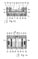
- the figure 2 is a cross-sectional view of an integrated circuit 1, at an electrostatic discharge protection device according to a first variant of a first embodiment of the invention.
- the integrated circuit 1 comprises other electronic components not illustrated here.
- the protection device is formed directly above a semiconductor substrate 91.
- This substrate 91 has, for example, a p-type doping.
- the protection device comprises an NPN bipolar transistor and a PNP bipolar transistor.
- the NPN transistor comprises an emitter 42, a collector 44 and a base 43.
- the emitter 42 includes an n-type doped semiconductor element.
- the collector 44 comprises an n-type doped semiconductor element, and the base 43 comprises a p-type doped semiconductor element.
- the PNP transistor has an emitter 45. This emitter 45 includes a p-type doped semiconductor element.
- the base of the PNP transistor is merged with the collector 44 of the NPN transistor (hereinafter denoted by the reference 44), and the collector of the PNP transistor coincides with the base 43 of the NPN transistor, a thyristor being thus formed.
- the emitters 42 and 45 advantageously have respective dopings N + and P +.
- the emitters 42 and 45 and the bases 43 and 44 are formed in a semiconductor layer (here in silicon) disposed on a buried insulating layer 2 having a thickness less than or equal to 50 nm.
- a semiconductor layer here in silicon
- the NPN and PNP transistors are advantageously coplanar.
- coplanar means that one can define a plane passing through the emitters, bases and collectors of these transistors, this plane being parallel to the buried insulating layer 2.
- the semiconductor layer typically has a thickness less than or equal to 15 nm, preferably less than 10 nm, and advantageously less than or equal to 7 nm.
- Such a semiconductor layer thickness facilitates the electrostatic control of the bases 43 and 44 by ground planes 93 and 94. These thicknesses typically correspond to the thickness of a semiconductor layer on the buried insulating layer 2 before a recovery. epitaxy.
- Transmitters 42 and 45 are respectively connected to electrodes K and A of the electrostatic discharge protection device.
- Metal contacts 32 and 33 are for this purpose in contact with the emitters 42 and 45 respectively.
- the NPN and PNP transistors are thus configured to selectively conduct a discharge current between the electrodes K and A, as detailed below.
- the electrostatic discharge protection device further comprises a first semiconductor ground plane 93 and a second semiconductor ground plane 94.
- the first and second ground planes 93 and 94 are arranged under the buried insulating layer 2.
- the first ground plane 93 extends to the base of the base 43.
- the first ground plane 93 has a doping of identical type to that of the base 43, so a p-type doping.
- the second ground plane 94 extends to the base of the base 44.
- the second ground plane 94 has an identical type of doping to that of the base 43, so n-type doping.
- the ground planes 93 and 94 are electrically biased.
- the electric polarization of the ground plane 93 is applied via an implanted zone 41 with p-type doping (and advantageously with P + type doping) and via a metal contact 31.
- a polarization Gp is applied to the metal contact 31 via a polarization circuit not shown here.
- the electric polarization of the ground plane 94 is applied via an implanted zone 46 with n-type doping (and advantageously with N + type doping) and via a metal contact 34.
- a polarization Gn is applied to the metal contact 34 via the bias circuit.
- the device for protecting against electrostatic discharges advantageously comprises, at its periphery, insulating trenches 61 and 64 extending in depth to the substrate 91.
- the protection device advantageously furthermore comprises an isolation trench 62 separating the emitter 42 of the implanted zone 41.
- the isolation trench 62 extends in depth to the buried insulating layer 2.
- the protection device also advantageously comprises an isolation trench 63 separating the emitter 45 from the implanted zone 46.
- the isolation trench 63 extends in depth to the buried insulating layer 2.
- the isolation trenches 61 and 64 extend more deeply than the isolation trenches 62 and 63.
- 93 and 94 ground planes respectively extend under the isolation trenches 62 and 63, until contact with the implanted zones 41 and 46 respectively.
- the use of insulation trenches d e different depths makes it possible to reduce the number of implantation steps, the polarization of the ground planes 93 and 94 by electrodes then requiring a smaller number of
- the figure 5 is a top view of the protection device against electrostatic discharges.
- the isolation trenches 61 to 64 have not been illustrated.
- the doping density of the bases 43 and 44 is at least ten times lower than the doping density of the ground planes 93 and 94, respectively. Such doping can be obtained during the respective implantations of the ground planes 93 and 94.
- the Doping density of the same type in the semiconductor disposed on the buried insulating layer 2 is sufficient to form a base of a bipolar transistor. The lower the residual doping of the bases 43 and 44 at the end of this implantation, the lower the low polarization voltage levels can be applied to the ground planes 93 and 94.
- the doping of the bases 43 and 44 typically has a density less than 10 18 cm -3 , preferably less than 5 * 10 17 cm -3 .
- the buried insulating layer advantageously has a thickness less than or equal to 25 nm, or even less than or equal to 15 nm.
- the upper face of the bases 43 and 44 is set back with respect to the upper face of the emitters 42 and 45.
- the formation of the emitters 42 and 45 may for example be continued during an epitaxial recovery phase for forming emitters 42 and 45 higher than bases 43 and 44.
- the figure 6 is an approximation of the electrical diagram equivalent to the electrostatic discharge protection device of the first embodiment.
- the respective polarizations applied to the ground planes 93 and 94 make it possible to provide electrostatic control of the bases 43 and 44.
- This electrostatic control makes it possible on the one hand to reduce the leakage current when the protection device is not activated and also to modulate the respective trip voltages of the NPN and PNP transistors during an electrostatic discharge, in particular in the absence of a control electrode of one or both bases 43 and 44.
- the bias circuit may apply a voltage Gnd on the ground plane 93 and on the ground plane 94, in particular when the doping of the bases 43 and 44 is less than 10 18 cm -3 .
- the triggering of the NPN and PNP transistors is then not blocked to enable tripping in the presence of an electrostatic discharge.
- the trigger threshold voltage can be adjusted by changing the amplitude of a value Vp and applying -Vp on the ground plane 93 and + Vp on the ground plane 94. The higher the value of Vp, the more raises the trip voltage of the NPN and PNP transistors.
- the tripping voltage can be set using a small value of Vp, typically less than or equal to a logic circuit supply voltage Vdd or integrated circuit memory 1 It is also possible to apply a voltage Gnd on the ground plane 93 and a voltage + Vp on the ground plane 94. It is also possible to apply a negative voltage Vp1 to the ground plane 93 and a positive voltage Vp2 to the ground plane. 94, with different amplitudes for Vp1 and Vp2. The behavior of the protective device during the occurrence of an electrostatic discharge can therefore easily be adjusted.
- the bias circuit can apply the voltage -Vdd to the ground plane 93 and the voltage Vdd to the ground plane 94, Vdd being for example equal to 1 V.
- Vdd being for example equal to 1 V.
- the doping of the majority carriers in the bases 43 and 44 can however be defined sufficiently high (for example close to 10 18 cm -3 ) for reduce the leakage current passing through them with polarization levels of the ground planes even lower.
- the figure 3 is a cross-sectional view of a second variant of the electrostatic discharge protection device of the first embodiment.
- This variant incorporates all the features of the first variant, the only difference being that the upper faces of the bases 43 and 44 are flush with the upper faces of the emitters 42 and 45.
- the formation of the bases 43 and 44 and the emitters 42 and 42 45 may for example be continued during the same phase of epitaxial recovery.
- Such a variant makes it possible to reduce the conduction resistance as far as possible through the bases 43 and 44 and thus to increase the maximum intensity of a short circuit during an electrostatic discharge.
- the thickness of the bases 43 and 44 resulting from an epitaxial resumption is advantageously less than or equal to 25 nm, and preferably less than or equal to 22 nm, in order to maintain an electrostatic control of the bases 43 and 44 optimal by the planes of mass 93 and 94.
- an annealing step makes it possible to diffuse the dopants of each of the bases 43 and 44 in their upper part obtained by epitaxy.
- the ground planes 93 and 94 are in contact.
- the polarization voltage Gp is at most equal to the polarization voltage Gn.
- the plans of mass 93 and 94 have respective projections (according to the normal to the buried insulating layer) on the buried insulating layer 2 which include the respective projections of the bases 43 and 44 on this buried insulating layer. This maximizes the electrostatic control of the ground planes 93 and 94 on the bases 43 and 44.
- the bases 43 and 44 are devoid of metal contact or electrode contact.
- the dopant concentration of the transmitters 42 and 45 is at least equal to 10 20 cm -3, preferably at least 5 * 10 20 cm -3, and preferably at least 10 21 cm -3.
- the dopant concentration of the bases 43 and 44 is between 5 * 10 16 cm -3 and 5 * 10 17 cm -3 .
- the other electronic components of the integrated circuit 1 may for example comprise transistors of FDSOI type, arranged on the same buried insulating layer 2 as the protection device. These FDSOI transistors may be arranged in line with respective polarized ground planes arranged under the buried insulating layer 2. In this technology, the doping of the transistor channel is almost zero (typically 10 15 cm -3 ).
- FIGS. 18 to 25 are cross-sectional views of an integrated circuit 1 according to the third variant of the first embodiment of the invention, during different steps of an example of a manufacturing method.
- a buried insulating layer 2 disposed on a semiconductor substrate 91 (typically silicon).
- a semiconductor layer 4 (typically a thin silicon layer having a thickness less than or equal to 10 nm, or even less than or equal to 7 nm) is disposed on the buried insulating layer 2.
- An oxide hard mask 71 is typically formed on the layer 4.
- the hard mask 71 has a composition and a thickness known per se.
- a nitride layer 72 is typically formed on the hard mask 71.
- the nitride layer 72 has a known composition and thickness.
- the integrated circuit 1 is shaped by photolithography so as to maintain the nitride 72, the hard mask 71, the layer 4 and the insulating layer 2 in the zone in which it is desired to form the NPN and PNP transistors of the protection device.
- the layers of nitride 72 and hard mask 71 are removed in particular in the areas where it is desired to form Bulk-type transistors by removing the buried insulating layer 2.
- epitaxy is advantageously carried out for the possible Bulk zones of the integrated circuit 1.
- the epitaxy is for example carried out to form a semiconducting silicon layer 73 flush with the layer 4.
- Insulating trenches 62 and 63 are formed and extend into the substrate 91 at the periphery of the layer 4.
- Insulation trenches 61 and 64 are formed and extend into the substrate 91.
- the isolation trenches 61 and 64 have the same depth as the isolation trenches 62 and 63.
- a semiconductor element extends between the trenches of the trenches. isolation 61 and 62 to the substrate 91.
- a semiconductor element extends between the isolation trenches 63 and 64 to the substrate 91.
- the materials for example silicon oxide
- the depths of the trenches insulation 61 to 64 are known per se.
- Insulation trenches 62 and 63 are formed and extend into substrate 91 at the periphery of layer 4. Insulation trenches 61 and 64 are formed and extend into substrate 91. Trenches In this variant, the insulation 61 and 64 have the same depth as the isolation trenches 62 and 63. A semiconductor element extends between the isolation trenches 61 and 62 as far as the substrate 91. A semiconductor element extends between the isolation trenches 63 and 64 to the substrate 91.
- the materials for example silicon oxide
- the depths of the isolation trenches 61 to 64 are known per se.
- An oxide hard mask 71 is then formed on the layer 4.
- a nitride layer 72 is then formed on the hard mask 71.
- the integrated circuit 1 is then shaped by photolithography so as to maintain the nitride 72, the hard mask 71, the layer 4 and the insulating layer 2 in the zone in which it is desired to form the NPN and PNP transistors of the protection device.
- the layers of nitride 72 and hard mask 71 are removed in particular in the areas where it is desired to form Bulk-type transistors by removing the buried insulating layer 2.
- an epitaxy is made for the possible Bulk zones of the integrated circuit 1.
- the epitaxy is for example made to form a semiconducting silicon layer 73 flush with the layer 4.
- the implantation of the ground plane 93 is typically carried out with a dose of between 10 12 cm -2 and 10 14 cm -2 of Indium, and an energy between 110 and 180 keV.
- the implantation of the ground plane 94 is typically carried out with a dose of between 10 12 cm -2 and 10 14 cm -2 of Arsenic, and an energy of between 90 and 150 keV.
- the implantation energies will of course be adjusted according to the thickness of the layer 2 and the film 4.
- a casing 95 doped p type was implanted under the ground plane 93 and extends under the isolation trench 62 into the semiconductor element disposed between the isolation trenches 61 and 62.
- a Type doped box 96 has been implanted under the ground plane 94 and extends under the isolation trench 63 into the semiconductor element disposed between the isolation trenches 63 and 64.
- the implantation of the ground plane 93 is configured to have a maximum density of implantation under the buried insulating layer 2 and in this ground plane 93, this implantation also induces a p-type doping in the layer 4 to the Plumb with the ground plane 93 (zone 412) and in the upper part of the semiconductor element present between the isolation trenches 61 and 62.
- the implantation of the ground plane 94 is configured to have a maximum density of implantation under the buried insulating layer 2 and in this ground plane 94, this implantation also induces an n-type doping in the layer 4 in line with the ground plane 94 (area 413) and in the upper part of the semiconductor element present between the isolation trenches 63 and 64.
- an epitaxial resumption was made to increase the thickness of silicon on the semiconductor element present between the isolation trenches 61 and 62, on the semiconductor element present between the isolation trenches 63 and 64, on a part of the zone 412 in contact with the trench 62, and on a part of the zone 413 in contact with the trench 63.
- the zones on which it is not desired to carry out epitaxy are typically protected by a mask hard (not shown).
- An implanted zone 41 is formed by P + type doping
- the emitter 42 is formed by N + type doping
- the emitter 45 is formed by P + doping
- the implanted zone 46 is formed by N + doping.
- the structure of the bipolar transistors NPN and PNP and the corresponding thyristor are thus available.
- the doping of at least one of the bases formed during the implantation of one of the ground planes is maintained.
- the doping of at least one of the two bases is therefore performed during the implantation of its ground plane.
- the residual doping of this base after the implantation of its ground plane typically has a density of less than 10 18 cm -3 , preferably less than 5 * 10 17 cm -3 .
- at least one of the two bases is no longer being implanted, for example by maintaining at least one of these two bases masked during any subsequent implantation step.
- interconnections are made with the metal contacts 31 to 34.
- the metal contacts 31 and 34 are connected to a bias circuit.
- the doping in the bases 43 and 44 still corresponds to doping after the implantation of the ground planes 93 and 94.
- the base 44 of the structure obtained at the figure 23 is the subject of an additional implementation type LDD (for lowly doped drain in English, for a doping typically between 10 18 cm -3 and 10 19 cm -3 ).
- LDD for lowly doped drain in English, for a doping typically between 10 18 cm -3 and 10 19 cm -3 .
- the figure 7 is a cross-sectional view of an integrated circuit 1, at an electrostatic discharge protection device according to a first variant of a second embodiment of the invention.
- the integrated circuit 1 comprises other electronic components not illustrated here.
- the doping density of the base 43 is at least 10 times less than the doping density of the ground plane 93.
- the doping density of the base 44 can also be at least 10 times less than the doping density of the ground plane. 94.
- the doping of the base 43 being of the same type as that of the ground plane 93, its doping can be obtained during the implantation of the ground plane 93.
- the doping density of the same type in the semiconductor disposed on the buried insulating layer 2 is sufficient to form the base 43.
- the doping of the base 44 being of a type opposite to that of the ground plane 94, the base 44 is the subject of an implantation with n-type doping posterior to the implantation of the ground planes 93 and 94.
- the doping of the base 44 may typically be LDD type doping.
- the doping density of the base 44 is then typically greater than the doping density of the base 43.
- the second embodiment makes it possible to produce the ground planes 93 and 94 during the same implantation step. Furthermore, the manufacturing method and the control of the protection device are simplified, since the same bias voltage is applied to the ground planes 93 and 94, preferably with the same metal contact.
- the electrostatic control of the base 43 by the ground plane 93 is preponderant compared to the electrostatic control of the base 44 by the ground plane 94.
- the doping density of the base 44 is at least 10 times less than the doping density of the ground plane 94.
- the doping density of the base 43 can also be at least 10 times less than the doping density of the ground plane. 93.
- the doping of the base 44 being of the same type as that of the ground plane 94, its doping can be obtained during the implantation of the ground plane 94.
- the doping density of the same type in the semiconductor disposed on the buried insulating layer 2 is sufficient to form the base 44.
- the doping of the base 43 being of a type opposite to that of the ground plane 93, the base 43 is the subject of a p-type doping implantation posterior to the implantation of the ground planes 93 and 94.
- doping of the base 43 may typically be LDD type doping.
- the doping density of the base 43 is then typically greater than the doping density of the base 44.
- the electrostatic control of the base 44 by the ground plane 94 is preponderant compared to the electrostatic control of the base 43 by the ground plane 93.
- the figure 9 is a cross-sectional view of a third variant of the electrostatic discharge protection device of the second embodiment.
- This variant incorporates all the features of the first variant, the only difference being that the metal contact 33 extends up to the base of the base 44, in contact with the base 44.
- the base 43 is devoid of metal contact.
- the control of the base 44 is improved, the gain of the PNP transistor is modified (by lowering it), without increasing the size of the integrated circuit 1 nor increasing the complexity of its manufacturing process.
- the metal contact 32 extends to the base of the base 43, in contact with this base 43.
- the figure 10 is a cross-sectional view of a fourth variant of the electrostatic discharge protection device of the second embodiment.
- This variant incorporates all the features of the third variant, the only difference being that the metal contact 33 extends up to the base of the base 44, in contact with this base 44.
- the base 43 is devoid of metal contact.
- the control is improved of the base 44, the gain of the PNP transistor is modified, without increasing the size of the integrated circuit 1 nor increasing the complexity of its manufacturing process.
- the metal contact 32 extends to the base of the base 43, in contact with this base 43.
- the metal contact 32 extends to the base of the base 43, in contact with the base 43.
- the base 44 is then free of metal contact.
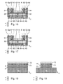
- the figure 11 is a cross-sectional view of a first variant of an electrostatic discharge protection device according to a third embodiment.
- the third embodiment is intended to form a TRIAC (for Triode for Alternating Current in English) to protect the integrated circuit regardless of the flow direction of the electrostatic discharge. This provides a bidirectional protection of the integrated circuit 1.
- the integrated circuit 1 comprises other electronic components not shown here.
- the protection device is formed directly above a semiconductor substrate 91.
- This substrate 91 has, for example, a p-type doping.
- the protection device comprises an NPN type bipolar transistor and a PNP type bipolar transistor to form a TRIAC.
- the NPN transistor comprises an emitter 42, a collector 47 and a base 43.
- the emitter 42 includes an n-type doped semiconductor element.
- the collector 47 comprises an n-type doped semiconductor element, and the base 43 comprises a p-type doped semiconductor element.
- the PNP transistor has a transmitter. This emitter includes a first p-type semiconductor element element 45 and a second p-type semiconductor element 44.
- the base of the PNP transistor is merged with the collector 47 of the NPN transistor (hereinafter referred to as 47), and the collector of the PNP transistor coincides with the base 43 of the NPN transistor.
- the emitter 42 and the first semiconductor element 45 advantageously have respective dopings N + and P +.
- Transmitters 42 and 44/45 and bases 43 and 47 are formed in a semiconductor layer (here in silicon) disposed on a buried insulating layer 2 having a thickness less than or equal to 50 nm.
- the NPN and PNP transistors are advantageously coplanar.
- the semiconductor layer typically has a thickness of less than or equal to 15 nm, preferably less than at 10 nm, and advantageously less than or equal to 7 nm.
- Such a semiconductor layer thickness facilitates the electrostatic control of the bases 43 and 47 by ground planes 93 and 97. These thicknesses typically correspond to the thickness of a semiconductor layer on the buried insulating layer 2 before a recovery. epitaxy.
- the emitters of the NPN and PNP transistors are respectively connected to electrodes K and A of the electrostatic discharge protection device.
- Metal contacts 32 and 33 are for this purpose in contact with the emitters of the NPN and PNP transistors respectively.
- the NPN and PNP transistors are thus configured to selectively conduct a discharge current between the electrodes K and A.
- the electrostatic discharge protection device further comprises a first semiconductor ground plane 93, a second semiconductor ground plane 94 and a third semiconductor ground plane 97.
- the first, second and third ground planes 93, 94 and 97 are arranged under the buried insulating layer 2.
- the first ground plane 93 extends to the base of the base 43.
- the first ground plane 93 presents a doping of identical type to that of the base 43, so p-type doping.
- the third ground plane 97 has a doping of identical type to that of the base 47, thus n-type doping.
- the second ground plane 94 extends vertically above the emitter including the semiconductor elements 44 and 45.
- the second ground plane 94 has a doping of the same type as that of these semiconductor elements 44 and 45. , therefore p-type doping.
- the ground planes 93, 94 and 97 are electrically biased.
- the electric polarization of the ground plane 93 is applied via an implanted zone 41 with p-type doping (and advantageously with P + type doping) and via a metal contact 31.
- a polarization Gp is applied to the metal contact 31 via a polarization circuit not shown here.
- the electric polarization of the ground plane 94 is applied via an implanted zone 46 with p-type doping (and advantageously with P + type doping) and via a metal contact 34.
- the polarization Gp is applied to the metal contact 34.
- the electric polarization of the ground plane 97 is applied via a non-illustrated, n-doped (and advantageously N + type doping) implanted zone and via a metal contact 35.
- a bias Gn is applied to the metal contact 35 via the bias circuit.
- This protection device against electrostatic discharges advantageously comprises at its periphery isolation trenches 61 and 64 extending in depth to the substrate 91.
- the protective device advantageously also comprises an isolation trench 62 separating the emitter 42 from the implanted zone 41.
- the isolation trench 62 extends in depth to the buried insulating layer 2.
- the protection device also advantageously comprises a isolation trench 63 separating the emitter of the PNP transistor from the implanted zone 46.
- the isolation trench 63 extends in depth to the buried insulating layer 2.
- the isolation trenches 61 and 64 extend deeper than isolation trenches 62 and 63.
- the ground planes 93 and 94 extend respectively under the isolation trenches 62 and 63, until they contact the implanted zones 41 and 46, respectively.
- the ground plane 97 extends along another axis under a trench. insulation not shown, until contact with an implanted area.
- the figure 12 is a top view of the protective device against electrostatic discharges of the figure 11 .
- the isolation trenches 61 to 64 have not been illustrated.
- the doping density of the bases 43 and 47 is at least ten times lower than the doping density of the ground planes 93 and 97, respectively. Such doping can be obtained during the respective implantations of the ground planes 93 and 97.
- the density of the second semiconductor element 44 is at least ten times lower than the doping density of the ground plane 94.
- the doping density of the same type in the semiconductor disposed on the buried insulating layer 2 is sufficient to form a base of a bipolar transistor.
- the doping of the bases 43 and 47 typically has a density less than 10 18 cm -3 , preferably less than 5 * 10 17 cm -3 .
- the buried insulating layer advantageously has a thickness less than or equal to 25 nm, or even less than or equal to 15 nm.
- the upper face of the bases 43 and 47 and of the semiconductor element 44 is set back with respect to the upper face of the emitter 42 and of the semiconductor element 45.
- the formation of the The emitter 42 and the semiconductor element 45 may, for example, be continued during an epitaxial recovery phase.
- the figure 13 is a cross-sectional view of a second variant of a device for protection against electrostatic discharges according to a third embodiment.
- the figure 14 is a top view of the protective device against electrostatic discharges of the figure 13 .
- the isolation trenches 61 to 64 have not been illustrated.
- the figure 15 is a top view of a set of protective devices according to the figure 11 contiguous in an integrated circuit 1. This figure shows that the polarization of the ground planes 97 via metal contacts can be made jointly for several devices for protection against discharges, with a minimum of space.
- the isolation trenches 61 to 64 of the third embodiment have the same depth. It is also possible to envisage the upper faces of the semiconductor elements 43, 44 and 47 flush with the upper faces of the emitters 42 and 45. The doping of one of the semiconductor elements 43, 44 or 47 can also be of LDD type. .
- the figure 16 is a cross-sectional view of an integrated circuit 1, at an electrostatic discharge protection device according to a first variant of a fourth embodiment of the invention.
- the integrated circuit 1 comprises other electronic components not illustrated here.
- This variant differs from the first variant of the first embodiment only in the presence of an insulating element 65 extending between the buried insulating layer 2 and the substrate 91.
- the insulating element 65 is positioned at the The insulation member 65 extends into the substrate 91 more deeply than the ground planes 93 and 94.
- the element 65 extends here to the same depth as the isolation trenches 61 and 64.
- the insulation member 65 electrically isolates the ground planes 93 and 94 from each other. Such isolation reduces leakage between ground planes 93 and 94 and also reduces parasitic capacitances to improve high frequency performance. Furthermore, it is possible to use a wider variety of polarization potentials on the ground planes 93 and 94.
- the projections of the ground planes 93 and 94 on the layer 2 do not include the respective projections of the bases 43 and 44 on this layer 2.
- a sufficient proportion ground planes 93 and 94 remain at the base respectively of the bases 43 and 44 to ensure an electrostatic control thereof.
- the ground planes 93 and 94 extend vertically respectively from the emitter contacts 42 / base 43 and emitter 45 / base 44.
- the figure 17 is a cross-sectional view of an integrated circuit 1, at an electrostatic discharge protection device according to a second variant of the fourth embodiment of the invention.
- This variant differs from the first variant in that it further comprises another buried insulation layer 66, disposed under the ground planes 93 and 94 and extending between the isolation trenches 61 and 64.
- the buried insulation 66 electrically isolates the ground planes 93 and 94 of the substrate 91.
- the layer 66 also has a portion protruding between the ground planes 93 and 94 and extending to the buried insulating layer 2, so as to isolate the ground planes 93 and 94 from each other. Due to the insulation with respect to the substrate 91, it is thus possible to have a bias voltage of the ground plane 93 greater than the bias voltage of the ground plane 94.
- the substrate 91 and the semiconductor layer are made of silicon, other semiconductor materials can however also be used.
- the figure 26 provides diagrams illustrating the current density I A as a function of the anode voltage (VA) for different bias voltages V Gp of the ground plane placed beneath the p-type doped base.
- VA anode voltage
- the diagrams in the left-hand part of the figure correspond to the first variant of the second embodiment, with floating bases.
- the diagrams of the right part of the figure correspond to declination of this first variant of the second embodiment, in which the metal cathode 32 in contact with the implanted zone 42 overflows until contact with the base 43.
- This diagram confirms the great linearity between the polarization voltage Gp and the trigger voltage Vt1 (the trigger voltage is deduced from the diagrams at the intersection between these and a dashed segment), whether for a positive voltage Gp or negative. Furthermore, it can be seen that the control by a voltage Gp of between 0 and +1 V makes it possible to obtain a tripping voltage Vt1 of between 1 and 3.9V, depending on whether the base 43 is floating or whether the base 43 is short. connected to the metal cathode 32.
- the bases are not connected to a basic current control circuit.
Abstract
L'invention concerne un circuit intégré, comprenant un dispositif de protection contre les décharges électrostatiques incluant : -une couche isolante enterrée (2) comportant une épaisseur inférieure ou égale à 50nm ; -des premiers et deuxième transistors bipolaires disposés sur la couche isolante enterrée (2), un de ces transistors bipolaires étant un transistor NPN, l'autre de ces transistors étant un transistor PNP, la base du premier transistor bipolaire étant confondue avec le collecteur du deuxième transistor bipolaire et la base du deuxième transistor bipolaire étant confondue avec le collecteur du premier transistor bipolaire, les premier et deuxième transistors bipolaires étant configurés pour conduire sélectivement un courant de décharge entre deux électrodes (A, K) du dispositif de protection ; -un premier plan de masse semi-conducteur (93) disposé sous la couche isolante enterrée, adapté à être polarisé électriquement, s'étendant à l'aplomb de la base (43) du premier transistor bipolaire, présentant un premier type de dopage identique à celui de la base du premier transistor bipolaire et présentant une densité de dopage au moins dix fois supérieure à celle de la base du premier transistor bipolaire.An integrated circuit, comprising an ESD protection device including: a buried insulating layer (2) having a thickness less than or equal to 50 nm; first and second bipolar transistors disposed on the buried insulating layer (2), one of these bipolar transistors being an NPN transistor, the other of these transistors being a PNP transistor, the base of the first bipolar transistor being merged with the collector of the second bipolar transistor and the base of the second bipolar transistor being merged with the collector of the first bipolar transistor, the first and second bipolar transistors being configured to selectively conduct a discharge current between two electrodes (A, K) of the protection device; a first semiconductor mass plane (93) disposed under the buried insulating layer, adapted to be electrically biased, extending vertically above the base (43) of the first bipolar transistor, having a first identical type of doping to that of the base of the first bipolar transistor and having a doping density at least ten times greater than that of the base of the first bipolar transistor.
Description
L'invention concerne les circuits intégrés, et en particulier les circuits intégrés réalisés sur un substrat de type silicium sur isolant (SOI). La technologie SOI consiste à séparer une fine couche de silicium (quelques nanomètres) sur un substrat en silicium par une couche d'isolant relativement épaisse (quelques dizaines de nanomètres en règle générale).The invention relates to integrated circuits, and in particular integrated circuits made on a silicon-on-insulator (SOI) type substrate. SOI technology consists of separating a thin layer of silicon (a few nanometers) on a silicon substrate by a relatively thick insulating layer (a few tens of nanometers as a rule).
Les circuits intégrés réalisés en technologie SOI présentent un certain nombre d'avantages. De tels circuits présentent généralement une plus faible consommation électrique pour des performances équivalentes. De tels circuits induisent également des capacités parasites plus faibles, qui permettent d'améliorer la vitesse de commutation. De plus, le phénomène de déclenchement parasite (« latchup » en langue anglaise) rencontré par les transistors MOS en technologie Bulk peut être évité. De tels circuits s'avèrent donc particulièrement adaptés pour des applications de type SoC ou MEMS. On constate également que les circuits intégrés SOI sont moins sensibles aux effets des radiations ionisantes et s'avèrent ainsi plus fiables dans des applications où de telles radiations peuvent induire des problèmes de fonctionnement, notamment dans des applications spatiales. Les circuits intégrés SOI peuvent notamment comprendre des mémoires vives de type SRAM ou des portes logiques.Integrated circuits made in SOI technology have a number of advantages. Such circuits generally have lower power consumption for equivalent performance. Such circuits also induce lower parasitic capacitances, which make it possible to improve the switching speed. In addition, the phenomenon of latchup in the English language encountered by MOS transistors Bulk technology can be avoided. Such circuits are therefore particularly suitable for SoC or MEMS type applications. It can also be seen that the SOI integrated circuits are less sensitive to the effects of ionizing radiation and thus prove more reliable in applications where such radiations can induce operating problems, especially in space applications. The SOI integrated circuits can notably comprise SRAM-type random access devices or logic gates.
De façon connue, de tels circuits intégrés incluent également des dispositifs de protection contre des décharges électrostatiques (ESD, pour « Electrostatic Discharge » en langue anglaise) accidentelles et pouvant détériorer ces transistors.In known manner, such integrated circuits also include protection devices against electrostatic discharges (ESD for "Electrostatic Discharge" in English) accidental and can deteriorate these transistors.
La conception d'un dispositif ESD est réalisée pour respecter un certain nombre de contraintes technologiques. La
Lorsque la tension de déclenchement Vt1 est atteinte, le dispositif ESD se déclenche. Dans un premier temps, la tension aux bornes du dispositif ESD peut décroître, le courant le traversant continuant d'augmenter. Dans un second temps, la tension aux bornes du dispositif ESD croît, de même que le courant le traversant afin de court-circuiter le courant de décharge électrostatique. Durant ce second temps, le dispositif ESD doit présenter une résistance de conduction aussi faible que possible, afin de présenter une intensité maximale de court-circuit It2 aussi élevée que possible pour une tension inférieure à la tension Vm.When the trigger voltage Vt1 is reached, the ESD device is triggered. At first, the voltage across the ESD device can decrease, the current passing through it continues to increase. In a second As a result, the voltage across the ESD increases, as does the current flowing through it, in order to short-circuit the electrostatic discharge current. During this second time, the ESD device must have a conduction resistance as low as possible, in order to have a maximum short circuit It2 as high as possible for a voltage lower than the voltage Vm.
Par ailleurs, le dispositif ESD doit également présenter un courant de fuite aussi faible que possible avant son déclenchement, afin de réduire la consommation électrique du circuit intégré.Furthermore, the ESD device must also have a leakage current as low as possible before its release, to reduce the power consumption of the integrated circuit.
Les dispositifs ESD occupent souvent une surface non négligeable du circuit intégré, qu'il est souhaitable de minimiser. Par ailleurs, le procédé de fabrication d'un dispositif ESD doit induire un minimum d'étapes supplémentaires pour ne pas accroître excessivement le coût du circuit intégré.ESD devices often occupy a significant area of the integrated circuit, which it is desirable to minimize. Furthermore, the method of manufacturing an ESD device must induce a minimum of additional steps to not excessively increase the cost of the integrated circuit.
Le document
Ce dispositif ESD présente cependant plusieurs inconvénients. Un circuit additionnel est nécessaire pour assurer le contrôle en courant de décharge par l'intermédiaire du transistor MOS, ce qui induit une baisse de densité d'intégration et une complexité accrue du circuit intégré. Un tel dispositif ESD présente en outre une grande complexité d'interconnexion, et nécessite d'optimiser le dopage des bases, ce qui implique donc d'utiliser un grand nombre de masques de photolithographie.This ESD device, however, has several disadvantages. An additional circuit is required to provide the discharge current control through the MOS transistor, which results in lower integration density and increased complexity of the integrated circuit. Such an ESD device also has a great complexity of interconnection, and requires optimizing the doping bases, which implies to use a large number of photolithography masks.
Le document
Ce dispositif ESD présente cependant plusieurs inconvénients. Un circuit additionnel est nécessaire pour assurer le contrôle en courant de décharge par l'intermédiaire du transistor MOS, ce qui induit une baisse de densité d'intégration et une complexité accrue du circuit intégré. Par ailleurs, ce circuit présente une fiabilité détériorée, liée au dimensionnement de l'oxyde de grille du transistor MOS formé sur le transistor NPN. La présence du transistor MOS induit en outre une réduction d'épaisseur des transistors NPN et PNP, et par conséquent une augmentation de la résistance de conduction lors du déclenchement du dispositif ESD. Un tel dispositif ESD présente en outre une grande complexité d'interconnexion, et nécessite d'optimiser le dopage des bases, ce qui implique donc d'utiliser un grand nombre de masques de photolithographie.This ESD device, however, has several disadvantages. An additional circuit is required to provide the discharge current control through the MOS transistor, which results in lower integration density and increased complexity of the integrated circuit. Moreover, this circuit has a deteriorated reliability, related to the sizing of the gate oxide of the MOS transistor formed on the NPN transistor. The presence of the MOS transistor furthermore induces a reduction in the thickness of the NPN and PNP transistors, and consequently an increase in the conduction resistance during the triggering the ESD device. Such an ESD device also has a great complexity of interconnection, and requires optimizing the doping bases, which implies to use a large number of photolithography masks.
Il existe un besoin pour un circuit intégré incluant un dispositif de protection contre les décharges électrostatiques résolvant un ou plusieurs de ces inconvénients. L'invention porte ainsi sur un circuit intégré comprenant un dispositif de protection contre les décharges électrostatiques, comprenant :
- une couche isolante enterrée comportant une épaisseur inférieure ou égale à 50nm ;
- des premiers et deuxième transistors bipolaires disposés sur la couche isolante enterrée, un de ces transistors bipolaires étant un transistor NPN, l'autre de ces transistors étant un transistor PNP, la base du premier transistor bipolaire étant confondue avec le collecteur du deuxième transistor bipolaire et la base du deuxième transistor bipolaire étant confondue avec le collecteur du premier transistor bipolaire, les premier et deuxième transistors bipolaires étant configurés pour conduire sélectivement un courant de décharge entre deux électrodes du dispositif de protection ;
- un premier plan de masse semi-conducteur disposé sous la couche isolante enterrée, adapté à être polarisé électriquement, s'étendant à l'aplomb de la base du premier transistor bipolaire, présentant un premier type de dopage identique à celui de la base du premier transistor bipolaire et présentant une densité de dopage au moins dix fois supérieure à celle de la base du premier transistor bipolaire.
- a buried insulating layer having a thickness of less than or equal to 50 nm;
- first and second bipolar transistors disposed on the buried insulating layer, one of these bipolar transistors being an NPN transistor, the other of these transistors being a PNP transistor, the base of the first bipolar transistor being merged with the collector of the second bipolar transistor, and the base of the second bipolar transistor being merged with the collector of the first bipolar transistor, the first and second bipolar transistors being configured to selectively conduct a discharge current between two electrodes of the protection device;
- a first semiconductor mass plane disposed under the buried insulating layer, adapted to be electrically biased, extending vertically above the base of the first bipolar transistor, having a first type of doping identical to that of the base of the first bipolar transistor and having a doping density at least ten times greater than that of the base of the first bipolar transistor.
Selon une variante, la densité de dopage dans la base du premier transistor bipolaire est inférieure ou égale à 1018cm-3.According to one variant, the doping density in the base of the first bipolar transistor is less than or equal to 10 18 cm -3 .
Selon encore une variante, les bases des premier et deuxième transistors bipolaires sont formés dans une couche semi-conductrice présentant une épaisseur inférieure ou égale à 15nm.According to another variant, the bases of the first and second bipolar transistors are formed in a semiconductor layer having a thickness less than or equal to 15 nm.
Selon une autre variante, le circuit intégré comprend un deuxième plan de masse semi-conducteur disposé sous la couche d'isolant enterrée, polarisé électriquement, présentant un deuxième type de dopage et s'étendant à l'aplomb de la base du deuxième transistor bipolaire, lesdits premier et deuxième types de dopage étant différents.According to another variant, the integrated circuit comprises a second semiconductor ground plane disposed under the electrically polarized buried insulator layer, having a second type of doping and extending vertically above the base of the second bipolar transistor. said first and second types of doping being different.
Selon encore une autre variante, lesdits premiers et deuxième plans de masse sont en contact.According to yet another variant, said first and second ground planes are in contact.
Selon une variante, les projections respectives des premier et deuxième plans de masse sur la couche isolante enterrée incluent les projections respectives des bases des premier et deuxième transistors bipolaires sur la couche isolante enterrée.According to a variant, the respective projections of the first and second ground planes on the buried insulating layer include the respective projections of the bases of the first and second bipolar transistors on the buried insulating layer.
Selon encore une variante, le circuit intégré comprend en outre un élément isolant électriquement, cet élément séparant les premier et deuxième plans de masse et étant disposé à l'aplomb de la jonction entre la base du premier transistor bipolaire et la base du deuxième transistor bipolaire.According to another variant, the integrated circuit furthermore comprises an electrically insulating element, this element separating the first and second ground planes and being disposed vertically above the junction between the base of the first bipolar transistor and the base of the second bipolar transistor. .
Selon une autre variante, ledit premier transistor bipolaire est dépourvu d'électrode en contact avec sa base.According to another variant, said first bipolar transistor is devoid of an electrode in contact with its base.
Selon encore une autre variante, les faces supérieures des bases et des émetteurs desdits premier et deuxième transistors bipolaires sont affleurantes.According to yet another variant, the upper faces of the bases and emitters of said first and second bipolar transistors are flush.
Selon une variante, le circuit intégré comprend en outre un transistor FDSOI formé sur ladite couche isolante enterrée et un plan de masse semi-conducteur disposé sous ladite couche isolante enterrée à l'aplomb dudit transistor FDSOI.According to one variant, the integrated circuit further comprises an FDSOI transistor formed on said buried insulating layer and a semiconductor ground plane disposed beneath said buried insulating layer in line with said FDSOI transistor.
L'invention porte aussi sur un procédé de fabrication d'un circuit intégré comprenant un dispositif de protection contre les décharges électrostatiques, comprenant :
- l'implantation d'un premier type de dopage dans un substrat semi-conducteur disposé sous une couche isolante enterrée, la couche isolante enterrée présentant une épaisseur inférieure ou égale à 50nm, de façon à former un premier plan de masse ,
- la formation de premier et deuxième transistors bipolaires dont un transistor NPN et un transistor PNP sur la couche isolante enterrée, la base du premier transistor présentant le premier type de dopage et les bases respectives des premier et deuxième transistors bipolaires étant confondues avec les collecteurs respectifs des deuxième et premier transistors bipolaires, la base du premier transistor bipolaire étant formée à l'aplomb du premier plan de masse, le dopage de la base du premier transistor étant réalisé durant l'implantation du premier type de dopage de formation dudit premier plan de masse, la densité de dopage à l'issue de l'implantation dans le premier plan de masse étant au moins dix fois supérieure à celle de la base du premier transistor bipolaire.
- implanting a first type of doping in a semiconductor substrate disposed under a buried insulating layer, the buried insulating layer having a thickness of less than or equal to 50 nm, so as to form a first ground plane,
- forming first and second bipolar transistors including an NPN transistor and a PNP transistor on the buried insulating layer, the base of the first transistor having the first type of doping and the respective bases of the first and second bipolar transistors being merged with the respective collectors of the second and first bipolar transistors, the base of the first bipolar transistor being formed in line with the first ground plane, the doping of the base of the first transistor being realized during the implantation of the first type of formation doping of said first ground plane , the doping density at the end of the implantation in the first ground plane being at least ten times greater than that of the base of the first bipolar transistor.
Selon une variante, le procédé comprend des étapes de :
- formation d'une électrode connectée électriquement avec ledit premier plan de masse ;
- interconnexion de ladite électrode avec un circuit de polarisation.
- forming an electrode electrically connected to said first ground plane;
- interconnecting said electrode with a bias circuit.
Selon une autre variante, la densité de dopage dans la base du premier transistor après la formation de l'interconnexion avec le circuit de polarisation est inférieure ou égale à 1018cm-3.According to another variant, the doping density in the base of the first transistor after the formation of the interconnection with the bias circuit is less than or equal to 10 18 cm -3 .
Selon encore une variante, les premier et deuxième transistors bipolaires sont formés dans une couche semi-conductrice disposée sur ladite couche isolante enterrée, le procédé comprenant des étapes d'implantation de dopage dans la couche semi-conductrice, ces étapes d'implantation étant postérieures à l'implantation de formation dudit premier plan de masse, la base du premier transistor bipolaire étant masquée durant chacune de ces étapes d'implantation postérieures.According to another variant, the first and second bipolar transistors are formed in a semiconductor layer disposed on said buried insulating layer, the method comprising doping implantation steps in the semiconductor layer, these implantation steps being subsequent. at the implantation of formation of said first ground plane, the base of the first Bipolar transistor being masked during each of these posterior implantation steps.
Selon encore une autre variante, le procédé de fabrication est dépourvu d'étape de formation d'une électrode en contact avec la base dudit premier transistor bipolaire.According to yet another variant, the manufacturing method is devoid of a step of forming an electrode in contact with the base of said first bipolar transistor.
D'autres caractéristiques et avantages de l'invention ressortiront clairement de la description qui en est faite ci-après, à titre indicatif et nullement limitatif, en référence aux dessins annexés, dans lesquels :
- la
figure 1 est un exemple de diagramme tension/courant d'un dispositif ESD de l'état de la technique durant une décharge ; - les
figures 2 à 4 sont des vues en coupe transversales de différentes variantes d'un premier mode de réalisation d'un dispositif de protection contre les décharges électrostatiques selon l'invention ; - la
figure 5 est une vue de dessus schématique du dispositif de protection desfigures 2 ;et 3 - la
figure 6 est un schéma électrique équivalent au dispositif de protection desfigures 2 à 4 ; - les
figures 7 à 10 sont des vues en coupe transversales de différentes variantes d'un deuxième mode de réalisation d'un dispositif de protection contre les décharges électrostatiques selon l'invention ; - la
figure 11 est une vue en coupe transversale d'une première variante d'un troisième mode de réalisation d'un dispositif de protection contre les décharges électrostatiques selon l'invention ; - la
figure 12 est une vue de dessus du dispositif de lafigure 11 ; - la
figure 13 est une vue en coupe transversale d'une deuxième variante d'un troisième mode de réalisation d'un dispositif de protection contre les décharges électrostatiques selon l'invention ; - la
figure 14 est une vue de dessus du dispositif de lafigure 13 ; - la
figure 15 est une vue de dessus d'un ensemble de dispositifs selon lafigure 11 accolés dans un circuit intégré ; - les
figures 16 à 17 sont des vues en coupe transversales de différentes variantes d'un quatrième mode de réalisation d'un dispositif de protection contre les décharges électrostatiques selon l'invention ; - les
figures 18 à 25 sont des vues en coupe transversales d'un circuit intégré selon la troisième variante du premier mode de réalisation de l'invention, durant différentes étapes d'un exemple de procédé de fabrication ; - la
figure 26 illustre des diagrammes de mesures de densités de courant en fonction de la tension d'anode, pour différentes tensions de polarisation de plans de masse.
- the
figure 1 is an example of a voltage / current diagram of an ESD device of the state of the art during a discharge; - the
Figures 2 to 4 are cross-sectional views of different variants of a first embodiment of an electrostatic discharge protection device according to the invention; - the
figure 5 is a schematic top view of the protective device of theFigures 2 and 3 ; - the
figure 6 is a circuit diagram equivalent to the protection device of theFigures 2 to 4 ; - the
Figures 7 to 10 are cross-sectional views of different variants of a second embodiment of a device for protection against electrostatic discharges according to the invention; - the
figure 11 is a cross-sectional view of a first variant of a third embodiment of a device for protection against electrostatic discharges according to the invention; - the
figure 12 is a top view of the device of thefigure 11 ; - the
figure 13 is a cross-sectional view of a second variant of a third embodiment of a device for protection against electrostatic discharges according to the invention; - the
figure 14 is a top view of the device of thefigure 13 ; - the
figure 15 is a top view of a set of devices according to thefigure 11 contiguous in an integrated circuit; - the
Figures 16 to 17 are cross-sectional views of different variants of a fourth embodiment of an electrostatic discharge protection device according to the invention; - the
Figures 18 to 25 are cross-sectional views of an integrated circuit according to the third variant of the first embodiment of the invention, during different steps of an example of a manufacturing method; - the
figure 26 illustrates diagrams of current density versus anode voltage measurements for different ground plane polarization voltages.
L'invention propose un circuit intégré muni d'un dispositif de protection contre les décharges électrostatiques. Le dispositif de protection comprend des premiers et deuxième transistors bipolaires formés sur une couche isolante enterrée de type UTBOX dont l'épaisseur est inférieure ou égale à 50nm. Ces transistors sont configurés pour conduire sélectivement un courant de décharge entre deux électrodes du dispositif de protection. La base et le collecteur du premier transistor bipolaire sont confondus respectivement avec le collecteur et la base du deuxième transistor bipolaire. Ces transistors bipolaires sont configurés pour conduire sélectivement un courant de décharge entre deux électrodes du dispositif de protection.The invention proposes an integrated circuit provided with a protection device against electrostatic discharges. The protection device comprises first and second bipolar transistors formed on a buried insulating layer UTBOX type whose thickness is less than or equal to 50nm. These transistors are configured to selectively conduct a discharge current between two electrodes of the protection device. The base and the collector of the first bipolar transistor are respectively merged with the collector and the base of the second bipolar transistor. These bipolar transistors are configured to selectively conduct a discharge current between two electrodes of the protection device.
Un premier plan de masse semi-conducteur (aussi couramment appelé grille arrière) est disposé sous la couche isolante enterrée et est polarisé électriquement. Le premier plan de masse est disposé à l'aplomb de la base du premier transistor bipolaire et présente un type de dopage identique à celui de cette base. La densité du dopage de ce premier plan de masse est au moins 10 fois supérieure à celle de la base du premier transistor bipolaire, avantageusement au moins 50 fois supérieure.A first semiconductor ground plane (also commonly referred to as a back gate) is disposed under the buried insulating layer and is electrically biased. The first ground plane is disposed vertically above the base of the first bipolar transistor and has a doping type identical to that of this base. The density of the doping of this first ground plane is at least 10 times higher than that of the base of the first bipolar transistor, advantageously at least 50 times higher.
Un tel dispositif de protection contre les décharges électrostatiques permet de se dispenser d'une optimisation de la base d'un des transistors bipolaires, du fait du contrôle électrostatique de cette base par le premier plan de masse. Un tel dispositif de protection permet en outre d'utiliser un potentiel de polarisation du premier plan de masse relativement bas pour réaliser ce contrôle électrostatique.Such a protection device against electrostatic discharges makes it possible to dispense with an optimization of the base of one of the bipolar transistors, because of the electrostatic control of this base by the first ground plane. Such a protection device also makes it possible to use a polarization potential of the first relatively low ground plane to carry out this electrostatic control.
Il s'avère qu'un tel dispositif de protection contre les décharges électrostatiques présente un courant de fuite très réduit, même en utilisant le ou les mêmes niveaux de polarisation des plans de masse que pour l'alimentation des autres circuits du circuit intégré. Par ailleurs, un tel dispositif de protection contre les décharges électrostatiques présente une résistance de conduction réduite et un courant maximal de décharge élevé, et ce sans nécessiter de circuit de contrôle complexe. Un tel circuit de protection contre les décharges électrostatiques peut également être réalisé sans induire une complexité excessive de ses interconnexions. Avec un procédé de fabrication approprié, on peut ainsi réduire le nombre de masques de photolithographie nécessaires, en réalisant la base du premier transistor bipolaire durant l'implantation du dopage du premier plan de masse.It turns out that such a device for protection against electrostatic discharges has a very low leakage current, even using the same or the same levels of polarization of the ground planes as for the supply of the other circuits of the integrated circuit. Moreover, such a device for protecting against electrostatic discharges has a reduced conduction resistance and a high maximum discharge current, without the need for a complex control circuit. Such a protection circuit against electrostatic discharges can also be achieved without inducing excessive complexity of its interconnections. With a suitable manufacturing method, it is thus possible to reduce the number of photolithography masks required, by making the base of the first bipolar transistor during the implantation of the doping of the first ground plane.
La
Le dispositif de protection est formé à l'aplomb d'un substrat semi-conducteur 91. Ce substrat 91 a par exemple un dopage de type p. Le dispositif de protection comporte un transistor bipolaire de type NPN et un transistor bipolaire de type PNP.The protection device is formed directly above a
Le transistor NPN comporte un émetteur 42, un collecteur 44 et une base 43. L'émetteur 42 inclut un élément semi-conducteur à dopage de type n, Le collecteur 44 comprend un élément semi-conducteur à dopage de type n, et la base 43 comprend un élément semi-conducteur à dopage de type p. Le transistor PNP comporte un émetteur 45. Cet émetteur 45 inclut un élément semi-conducteur à dopage de type p. La base du transistor PNP est confondue avec le collecteur 44 du transistor NPN (on la désignera donc par la suite par la référence 44), et le collecteur du transistor PNP est confondu avec la base 43 du transistor NPN, un thyristor étant ainsi formé. Les émetteurs 42 et 45 présentent avantageusement des dopages respectifs N+ et P+. Les émetteurs 42 et 45 et les bases 43 et 44 sont formés dans une couche semi-conductrice (ici en silicium) disposée sur une couche isolante enterrée 2 présentant une épaisseur inférieure ou égale à 50 nm. Par isolation, on entendra dans la présente description une isolation électrique. Les transistors NPN et PNP sont avantageusement coplanaires. Par coplanaire, on entend que l'on peut définir un plan traversant les émetteurs, bases et collecteurs de ces transistors, ce plan étant parallèle à la couche isolante enterrée 2. La couche semi-conductrice présente typiquement une épaisseur inférieure ou égale à 15nm, de préférence inférieure à 10nm, et avantageusement inférieure ou égale à 7nm. Une telle épaisseur de couche semi-conductrice facilite le contrôle électrostatique des bases 43 et 44 par des plans de masse 93 et 94. Ces épaisseurs correspondent typiquement à l'épaisseur d'une couche semi-conductrice sur la couche isolante enterrée 2 avant une reprise d'épitaxie.The NPN transistor comprises an
Les émetteurs 42 et 45 sont connectés respectivement à des électrodes K et A du dispositif de protection contre les décharges électrostatiques. Des contacts métalliques 32 et 33 sont à cet effet en contact avec les émetteurs 42 et 45 respectivement. Les transistors NPN et PNP sont ainsi configurés pour conduire sélectivement un courant de décharge entre les électrodes K et A, comme détaillé par la suite.
Le dispositif de protection contre les décharges électrostatiques comprend en outre un premier plan de masse semi-conducteur 93 et un deuxième plan de masse semi-conducteur 94. Les premier et deuxième plans de masse 93 et 94 sont disposés sous la couche isolante enterrée 2. Le premier plan de masse 93 s'étend jusqu'à l'aplomb de la base 43. Le premier plan de masse 93 présente un dopage de type identique à celui de la base 43, donc un dopage de type p. Le deuxième plan de masse 94 s'étend jusqu'à l'aplomb de la base 44. Le deuxième plan de masse 94 présente un dopage de type identique à celui de la base 43, donc un dopage de type n. Les plans de masse 93 et 94 sont polarisés électriquement. La polarisation électrique du plan de masse 93 est appliquée par l'intermédiaire d'une zone implantée 41 à dopage de type p (et avantageusement à dopage de type P+) et par l'intermédiaire d'un contact métallique 31. Une polarisation Gp est appliquée sur le contact métallique 31 par l'intermédiaire d'un circuit de polarisation non illustré ici. La polarisation électrique du plan de masse 94 est appliquée par l'intermédiaire d'une zone implantée 46 à dopage de type n (et avantageusement à dopage de type N+) et par l'intermédiaire d'un contact métallique 34. Une polarisation Gn est appliquée sur le contact métallique 34 par l'intermédiaire du circuit de polarisation.The electrostatic discharge protection device further comprises a first
Le dispositif de protection contre les décharges électrostatiques comporte avantageusement à sa périphérie des tranchées d'isolation 61 et 64 s'étendant en profondeur jusqu'au substrat 91. Le dispositif de protection comporte en outre avantageusement une tranchée d'isolation 62 séparant l'émetteur 42 de la zone implantée 41. La tranchée d'isolation 62 s'étend en profondeur jusqu'à la couche isolante enterrée 2. Le dispositif de protection comporte en outre avantageusement une tranchée d'isolation 63 séparant l'émetteur 45 de la zone implantée 46. La tranchée d'isolation 63 s'étend en profondeur jusqu'à la couche isolante enterrée 2. Dans cette variante, les tranchées d'isolation 61 et 64 s'étendent plus profondément que les tranchées d'isolation 62 et 63. Les plans de masse 93 et 94 s'étendent respectivement sous les tranchées d'isolation 62 et 63, jusqu'en contact respectivement avec les zones implantées 41 et 46. L'utilisation de tranchées d'isolation de profondeurs différentes permet de diminuer le nombre d'étapes d'implantation, la polarisation des plans de masse 93 et 94 par des électrodes nécessitant alors un moins grand nombre d'étapes d'implantation.The device for protecting against electrostatic discharges advantageously comprises, at its periphery, insulating
La
La densité de dopage des bases 43 et 44 est au moins dix fois inférieure à la densité de dopage des plans de masse 93 et 94 respectivement. Un tel dopage peut être obtenu lors des implantations respectives des plans de masse 93 et 94. Ainsi, lors d'une implantation d'un plan de masse, avec une profondeur d'implantation maximale disposée sous la couche d'isolant enterrée 2, la densité de dopage de même type dans le semi-conducteur disposé sur la couche isolante enterrée 2 est suffisante pour former une base d'un transistor bipolaire. Plus le dopage résiduel des bases 43 et 44 à l'issue de cette implantation est faible, plus on peut appliquer des niveaux de tension de polarisation faibles sur les plans de masse 93 et 94. Le dopage des bases 43 et 44 présente typiquement une densité inférieure à 1018cm-3, de préférence inférieure à 5*1017cm-3. Pour accroître l'influence du contrôle électrostatique d'un plan de masse sur la base disposée à son aplomb, la couche isolante enterrée présente avantageusement une épaisseur inférieure ou égale à 25 nm, voire inférieur ou égale à 15 nm.The doping density of the
Dans cette variante, la face supérieure des bases 43 et 44 est en retrait par rapport à la face supérieure des émetteurs 42 et 45. La formation des émetteurs 42 et 45 peut par exemple être poursuivie lors d'une phase de reprise d'épitaxie pour former des émetteurs 42 et 45 plus hauts que les bases 43 et 44.In this variant, the upper face of the
La
Les polarisations respectives appliquées sur les plans de masse 93 et 94 permettent d'assurer un contrôle électrostatique des bases 43 et 44. Ce contrôle électrostatique permet d'une part de réduire le courant de fuite lorsque le dispositif de protection n'est pas activé et aussi de moduler les tensions de déclenchement respectives des transistors NPN et PNP lors d'une décharge électrostatique, en particulier en l'absence d'électrode de commande d'une ou des deux bases 43 et 44.The respective polarizations applied to the ground planes 93 and 94 make it possible to provide electrostatic control of the
Dans un premier mode de fonctionnement correspondant au mode de protection contre les décharges électrostatiques, le circuit de polarisation peut appliquer une tension Gnd sur le plan de masse 93 et sur le plan de masse 94, en particulier lorsque le dopage des bases 43 et 44 est inférieur à 1018cm-3. Le déclenchement des transistors NPN et PNP n'est alors pas bloqué pour permettre un déclenchement en présence d'une décharge électrostatique. On peut ajuster la tension de seuil de déclenchement en modifiant l'amplitude d'une valeur Vp et en appliquant -Vp sur le plan de masse 93 et +Vp sur le plan de masse 94. Plus la valeur de Vp est élevée, plus on relève la tension de déclenchement des transistors NPN et PNP. Du fait du contrôle électrostatique obtenu avec les plans de masse 93 et 94, la tension de déclenchement peut être fixée en utilisant une faible valeur de Vp, typiquement inférieure ou égale à une tension Vdd d'alimentation de circuits logiques ou mémoire du circuit intégré 1. On peut également appliquer une tension Gnd sur le plan de masse 93 et une tension +Vp sur le plan de masse 94. On peut encore appliquer une tension Vp1 négative sur le plan de masse 93 et une tension Vp2 positive sur le plan de masse 94, avec des amplitudes différentes pour Vp1 et Vp2. Le comportement du dispositif de protection lors de l'apparition d'une décharge électrostatique peut donc aisément être ajusté.In a first mode of operation corresponding to the protection mode against electrostatic discharges, the bias circuit may apply a voltage Gnd on the
Dans un second mode de fonctionnement correspondant au mode de fonctionnement normal du circuit intégré, le circuit de polarisation peut appliquer la tension -Vdd sur le plan de masse 93 et la tension Vdd sur le plan de masse 94, Vdd étant par exemple égal à 1 V. Ainsi, malgré le très faible dopage des bases 43 et 44, un courant de fuite très faible les traverse en fonctionnement normal du circuit intégré 1. Le dopage des porteurs majoritaires dans les bases 43 et 44 pourra cependant être défini suffisamment élevé (par exemple proche de 1018cm-3) pour réduire le courant de fuite les traversant avec des niveaux de polarisation des plans de masse encore plus bas.In a second operating mode corresponding to the normal operating mode of the integrated circuit, the bias circuit can apply the voltage -Vdd to the
La
Avantageusement, une étape de recuit permet de diffuser les dopants de chacune des bases 43 et 44 dans leur partie supérieure obtenue par épitaxie.Advantageously, an annealing step makes it possible to diffuse the dopants of each of the
La
un caisson 95 est en outre formé dans le substrat 91 à l'aplomb du plan de masse 93.Le caisson 95 s'étend sous la tranchée d'isolation 62.Le caisson 95 forme un élément semi-conducteur à dopage de type p reliant le plan de masse 93 à lazone implantée 41 ;un caisson 96 est en outre formé dans le substrat 91 à l'aplomb du plan de masse 94.Le caisson 96 s'étend sous la tranchée d'isolation 63.Le caisson 96 forme un élément semi-conducteur à dopage de type n reliant le plan de masse 94 à lazone implantée 46.
- a
box 95 is furthermore formed in thesubstrate 91 in line with theground plane 93. Thebox 95 extends under theisolation trench 62. Thebox 95 forms a p-type doping semiconductor element connecting theground plane 93 to the implantedzone 41; - a
box 96 is furthermore formed in thesubstrate 91 in line with theground plane 94. Thebox 96 extends under theisolation trench 63. Thebox 96 forms an n-type doping semiconductor element connecting theground plane 94 to the implantedarea 46.
Selon le premier mode de réalisation, les plans de masse 93 et 94 sont en contact. Pour éviter une conduction en direct de la diode formée entre les plans de masse 93 et 94, la tension de polarisation Gp est au plus égale à la tension de polarisation Gn. Selon ce premier mode de réalisation, les plans de masse 93 et 94 ont des projections respectives (selon la normale à la couche isolante enterrée) sur la couche isolante enterrée 2 qui incluent les projections respectives des bases 43 et 44 sur cette couche isolante enterrée. On maximise ainsi le contrôle électrostatique des plans de masse 93 et 94 sur les bases 43 et 44.According to the first embodiment, the ground planes 93 and 94 are in contact. To avoid direct conduction of the diode formed between the ground planes 93 and 94, the polarization voltage Gp is at most equal to the polarization voltage Gn. According to this first embodiment, the plans of
Dans les différentes variantes illustrées du premier mode de réalisation, les bases 43 et 44 sont dépourvues de contact métallique ou de contact d'électrode.In the various illustrated variants of the first embodiment, the
Avantageusement, la concentration de dopants des émetteurs 42 et 45 est au moins égale à 1020cm-3, de préférence, au moins égale à 5*1020cm-3, et avantageusement au moins égale à 1021cm-3. Avantageusement, la concentration de dopants des bases 43 et 44 est comprise entre à 5*1016cm-3 et 5*1017cm-3.Advantageously, the dopant concentration of the
Les autres composants électroniques du circuit intégré 1 peuvent par exemple comprendre des transistors de type FDSOI, disposés sur la même couche isolante enterrée 2 que le dispositif de protection. Ces transistors FDSOI peuvent être disposés à l'aplomb de plans de masse polarisés respectifs disposés sous la couche isolante enterrée 2. Dans cette technologie, le dopage du canal du transistor est quasiment nul (typiquement de 1015 cm-3).The other electronic components of the
Les
À la
À la
À la
À la
En variante de la séquence des étapes 18 à 21, on peut procéder comme suit :
- On dispose d'une couche isolante enterrée 2 disposée sur
un substrat semi-conducteur 91. Une couchesemi conductrice 4 est disposée sur la couche isolante enterrée 2.
- There is a buried insulating
layer 2 disposed on asemiconductor substrate 91. Asemiconductor layer 4 is disposed on the buried insulatinglayer 2.
Des tranchées d'isolation 62 et 63 sont formées et s'étendent jusque dans le substrat 91 à la périphérie de la couche 4. Des tranchées d'isolation 61 et 64 sont formées et s'étendent jusque dans le substrat 91. Les tranchées d'isolation 61 et 64 présentent dans cette variante une même profondeur que les tranchées d'isolation 62 et 63. Un élément semi-conducteur s'étend entre les tranchées d'isolation 61 et 62 jusqu'au substrat 91. Un élément semi-conducteur s'étend entre les tranchées d'isolation 63 et 64 jusqu'au substrat 91. Les matériaux (par exemple de l'oxyde de silicium) et les profondeurs des tranchées d'isolation 61 à 64 sont connus en soi.
Un masque dur d'oxyde 71 est ensuite formé sur la couche 4. Une couche de nitrure 72 est ensuite formée sur le masque dur 71.An oxide
On met ensuite en forme le circuit intégré 1 par photolithographie de façon à maintenir le nitrure 72, le masque dur 71, la couche 4 et la couche isolante 2 dans la zone dans laquelle on souhaite former les transistors NPN et PNP du dispositif de protection. Les couches de nitrure 72 et de masque dur 71 sont retirées notamment dans les zones où l'on souhaite former des transistors de type Bulk en retirant la couche isolante enterrée 2.The
Optionnellement, on réalise une épitaxie pour les éventuelles zones Bulk du circuit intégré 1. L'épitaxie est par exemple réalisée pour former une couche semi conductrice de silicium 73 affleurante avec la couche 4.Optionally, an epitaxy is made for the possible Bulk zones of the
À la
Par ailleurs, un caisson 95 à dopage de type p a été implanté sous le plan de masse 93 et s'étend sous la tranchée d'isolation 62 jusque dans l'élément semi-conducteur disposé entre les tranchées d'isolation 61 et 62. Un caisson 96 à dopage de type n a été implanté sous le plan de masse 94 et s'étend sous la tranchée d'isolation 63 jusque dans l'élément semi-conducteur disposé entre les tranchées d'isolation 63 et 64.Furthermore, a
Bien que l'implantation du plan de masse 93 soit configurée pour présenter une densité maximale d'implantation sous la couche isolante enterrée 2 et dans ce plan de masse 93, cette implantation induit également un dopage de type p dans la couche 4 à l'aplomb du plan de masse 93 (zone 412) et dans la partie supérieure de l'élément semi-conducteur présent entre les tranchées d'isolation 61 et 62.Although the implantation of the
De même, bien que l'implantation du plan de masse 94 soit configurée pour présenter une densité maximale d'implantation sous la couche isolante enterrée 2 et dans ce plan de masse 94, cette implantation induit également un dopage de type n dans la couche 4 à l'aplomb du plan de masse 94 (zone 413) et dans la partie supérieure de l'élément semi-conducteur présent entre les tranchées d'isolation 63 et 64.Similarly, although the implantation of the
À la
À l'issue des étapes illustrées à la
d'une base 43 ayant le même type de dopage que le plan de masse 93, mais avec une densité de dopage au moins 10 fois inférieure ;d'une base 44 ayant le même type de dopage que le plan de masse 94 et avec une densité de dopage au moins 10 fois inférieure.
- a base 43 having the same type of doping as the
ground plane 93, but with a doping density at least 10 times lower; - a base 44 having the same type of doping as the
ground plane 94 and with a doping density at least 10 times lower.
On dispose ainsi de la structure des transistors bipolaires NPN et PNP et du thyristor correspondant. Pour la suite du procédé, on conserve le dopage d'au moins d'une des bases formées durant l'implantation d'un des plans de masse. Le dopage d'au moins une des deux bases est donc réalisé durant l'implantation de son plan de masse. Le dopage résiduel de cette base à l'issue de l'implantation de son plan de masse présente typiquement une densité inférieure à 1018cm-3, de préférence inférieure à 5*1017cm-3. Ainsi, au moins une des deux bases ne fait plus l'objet d'une implantation, en maintenant par exemple au moins une de ces deux bases masquée lors de toute étape ultérieure d'implantation.The structure of the bipolar transistors NPN and PNP and the corresponding thyristor are thus available. For the rest of the process, the doping of at least one of the bases formed during the implantation of one of the ground planes is maintained. The doping of at least one of the two bases is therefore performed during the implantation of its ground plane. The residual doping of this base after the implantation of its ground plane typically has a density of less than 10 18 cm -3 , preferably less than 5 * 10 17 cm -3 . Thus, at least one of the two bases is no longer being implanted, for example by maintaining at least one of these two bases masked during any subsequent implantation step.
À la
- on a défini un masque de protection en définissant les emplacements des contacts métalliques de polarisation ;
- on a procédé à une siliciuration ;
- on a déposé du métal pour former des contacts métalliques 31 à 34 respectivement sur la
zone implantée 41, l'émetteur 42, l'émetteur 45 et lazone implantée 46 ; - on a retiré le masque de protection.
- a protection mask has been defined by defining the locations of the bias metal contacts;
- silicidation was carried out;
- metal has been deposited to form
metal contacts 31 to 34 respectively on the implantedzone 41, thetransmitter 42, theemitter 45 and the implantedzone 46; - the protective mask was removed.
Lors d'étapes ultérieures, on réalise des interconnexions avec les contacts métalliques 31 à 34. Par exemple, les contacts métalliques 31 et 34 sont connectés à un circuit de polarisation. À ce stade, le dopage dans les bases 43 et 44 correspond encore au dopage à l'issue de l'implantation des plans de masse 93 et 94.In subsequent steps, interconnections are made with the
On peut constater que les avantages d'un circuit intégré 1 obtenu selon un tel procédé de fabrication n'induisaient pas nécessairement une complexification du procédé de fabrication. En effet, un tel procédé de fabrication permet d'utiliser un même masque pour l'implantation de dopants dans une base et dans un plan de masse.It can be seen that the advantages of an
À la
La
Cette variante reprend l'ensemble des caractéristiques de la troisième variante du premier mode de réalisation, les principales différences étant que :
- les plans de masse 93 et 94 sont confondus en un élément semi-conducteur à dopage de type p s'étendant sous les bases 43 et 44 et sous les émetteurs 42
et 45 ; - les caissons 95 et 96 sont remplacés
par un caisson 95 continu à dopage de type p s'étendant sous les plans de masse 93et 94, et sous les tranchées d'isolation 62 et 63 jusque dans les éléments semi-conducteur disposés respectivement entre les tranchées d'isolation 61et 62 et entre les tranchées d'isolation 63et 64.
- the ground planes 93 and 94 are combined into a p-type doped semiconductor element extending under the
bases emitters -
boxes continuous doping box 95 extending under the ground planes 93 and 94, and under theisolation trenches insulation trenches isolation trenches
La densité de dopage de la base 43 est au moins 10 fois inférieure à la densité de dopage du plan de masse 93. La densité de dopage de la base 44 peut également être au moins 10 fois inférieure à la densité de dopage du plan de masse 94. Le dopage de la base 43 étant de même type que celui du plan de masse 93, son dopage peut être obtenu lors de l'implantation du plan de masse 93. Ainsi, lors de l'implantation du plan de masse 93, avec une profondeur d'implantation maximale disposée sous la couche d'isolant enterrée 2, la densité de dopage de même type dans le semi-conducteur disposé sur la couche d'isolant enterrée 2 est suffisante pour former la base 43.The doping density of the
Le dopage de la base 44 étant d'un type opposé à celui du plan de masse 94, la base 44 fait l'objet d'une implantation à dopage de type n postérieure à l'implantation des plans de masse 93 et 94. Le dopage de la base 44 peut typiquement être un dopage de type LDD. La densité de dopage de la base 44 est alors typiquement supérieure à la densité de dopage de la base 43.The doping of the base 44 being of a type opposite to that of the
Le deuxième mode de réalisation permet de réaliser les plans de masse 93 et 94 durant une même étape d'implantation. Par ailleurs, le procédé de fabrication et la commande du dispositif de protection sont simplifiés, puisqu'une même tension de polarisation est appliquée sur les plans de masse 93 et 94, de préférence avec de même contact métallique.The second embodiment makes it possible to produce the ground planes 93 and 94 during the same implantation step. Furthermore, the manufacturing method and the control of the protection device are simplified, since the same bias voltage is applied to the ground planes 93 and 94, preferably with the same metal contact.
Dans cette variante du deuxième mode de réalisation, le contrôle électrostatique de la base 43 par le plan de masse 93 est prépondérant par rapport au contrôle électrostatique de la base 44 par le plan de masse 94.In this variant of the second embodiment, the electrostatic control of the base 43 by the
La
- les plans de masse 93 et 94 sont confondus en un élément semi-conducteur à dopage de type n s'étendant sous les bases 43 et 44 et sous les émetteurs 42
et 45 ; le caisson 95 est remplacépar un caisson 95 continu à dopage de type n s'étendant sous les plans de masse 93et 94, et sous les tranchées d'isolation 62 et 63 jusque dans les éléments semi-conducteur disposés respectivement entre les tranchées d'isolation 61et 62 et entre les tranchées d'isolation 63et 64.
- the ground planes 93 and 94 are merged into an n-type doped semiconductor element extending under the
bases emitters - the
casing 95 is replaced by a n-type dopingcontinuous casing 95 extending under the ground planes 93 and 94, and under theisolation trenches isolation trenches isolation trenches
La densité de dopage de la base 44 est au moins 10 fois inférieure à la densité de dopage du plan de masse 94. La densité de dopage de la base 43 peut également être au moins 10 fois inférieure à la densité de dopage du plan de masse 93. Le dopage de la base 44 étant de même type que celui du plan de masse 94, son dopage peut être obtenu lors de l'implantation du plan de masse 94. Ainsi, lors de l'implantation du plan de masse 94, avec une profondeur d'implantation maximale disposée sous la couche d'isolant enterrée 2, la densité de dopage de même type dans le semi-conducteur disposé sur la couche d'isolant enterrée 2 est suffisante pour former la base 44.The doping density of the
Le dopage de la base 43 étant d'un type opposé à celui du plan de masse 93, la base 43 fait l'objet d'une implantation à dopage de type p postérieure à l'implantation des plans de masse 93 et 94. Le dopage de la base 43 peut typiquement être un dopage de type LDD. La densité de dopage de la base 43 est alors typiquement supérieure à la densité de dopage de la base 44.The doping of the base 43 being of a type opposite to that of the
Dans cette variante du deuxième mode de réalisation, le contrôle électrostatique de la base 44 par le plan de masse 94 est prépondérant par rapport au contrôle électrostatique de la base 43 par le plan de masse 93.In this variant of the second embodiment, the electrostatic control of the base 44 by the
La
Quelle que soit la forme du contact métallique 33, on peut également envisager que le contact métallique 32 s'étend jusqu'à l'aplomb de la base 43, en contact avec cette base 43.Whatever the shape of the
La
Quelle que soit la forme du contact métallique 33, on peut également envisager que le contact métallique 32 s'étend jusqu'à l'aplomb de la base 43, en contact avec cette base 43.Whatever the shape of the
On peut également prévoir d'autres variantes à partir des première et deuxième variantes du deuxième mode de réalisation. En partant des première et deuxième variantes, on peut prévoir que le contact métallique 32 s'étend jusqu'à l'aplomb de la base 43, en contact avec cette base 43. La base 44 est alors dépourvue de contact métallique.It is also possible to provide other variants from the first and second variants of the second embodiment. From the first and second variants, it can be provided that the
La
Le dispositif de protection est formé à l'aplomb d'un substrat semi-conducteur 91. Ce substrat 91 a par exemple un dopage de type p. Le dispositif de protection comporte un transistor bipolaire de type NPN et un transistor bipolaire de type PNP pour former un TRIAC.The protection device is formed directly above a
Le transistor NPN comporte un émetteur 42, un collecteur 47 et une base 43. L'émetteur 42 inclut un élément semi-conducteur à dopage de type n, Le collecteur 47 comprend un élément semi-conducteur à dopage de type n, et la base 43 comprend un élément semi-conducteur à dopage de type p. Le transistor PNP comporte un émetteur. Cet émetteur inclut un élément premier élément semi-conducteur 45 à dopage de type p et un deuxième élément semi-conducteur 44 à dopage de type p. La base du transistor PNP est confondue avec le collecteur 47 du transistor NPN (on la désignera donc par la suite par la référence 47), et le collecteur du transistor PNP est confondu avec la base 43 du transistor NPN. L'émetteur 42 et le premier élément semi-conducteur 45 présentent avantageusement des dopages respectifs N+ et P+. Les émetteurs 42 et 44/45 et les bases 43 et 47 sont formés dans une couche semi-conductrice (ici en silicium) disposée sur une couche isolante enterrée 2 présentant une épaisseur inférieure ou égale à 50 nm. Les transistors NPN et PNP sont avantageusement coplanaires. La couche semi-conductrice présente typiquement une épaisseur inférieure ou égale à 15nm, de préférence inférieure à 10nm, et avantageusement inférieure ou égale à 7nm. Une telle épaisseur de couche semi-conductrice facilite le contrôle électrostatique des bases 43 et 47 par des plans de masse 93 et 97. Ces épaisseurs correspondent typiquement à l'épaisseur d'une couche semi-conductrice sur la couche isolante enterrée 2 avant une reprise d'épitaxie.The NPN transistor comprises an
Les émetteurs des transistors NPN et PNP sont connectés respectivement à des électrodes K et A du dispositif de protection contre les décharges électrostatiques. Des contacts métalliques 32 et 33 sont à cet effet en contact avec les émetteurs des transistors NPN et PNP respectivement. Les transistors NPN et PNP sont ainsi configurés pour conduire sélectivement un courant de décharge entre les électrodes K et A.The emitters of the NPN and PNP transistors are respectively connected to electrodes K and A of the electrostatic discharge protection device.
Le dispositif de protection contre les décharges électrostatiques comprend en outre un premier plan de masse semi-conducteur 93, un deuxième plan de masse semi-conducteur 94 et un troisième plan de masse semi-conducteur 97.The electrostatic discharge protection device further comprises a first
Les premier, deuxième et troisième plans de masse 93, 94 et 97 sont disposés sous la couche isolante enterrée 2. Le premier plan de masse 93 s'étend jusqu'à l'aplomb de la base 43. Le premier plan de masse 93 présente un dopage de type identique à celui de la base 43, donc un dopage de type p. Le troisième plan de masse 97 présente un dopage de type identique à celui de la base 47, donc un dopage de type n.The first, second and third ground planes 93, 94 and 97 are arranged under the buried insulating
Le deuxième plan de masse 94 s'étend à l'aplomb de l'émetteur incluant les éléments semi-conducteurs 44 et 45. Le deuxième plan de masse 94 présente un dopage de type identique à celui de ces éléments semi-conducteurs 44 et 45, donc un dopage de type p. Les plans de masse 93, 94 et 97 sont polarisés électriquement. La polarisation électrique du plan de masse 93 est appliquée par l'intermédiaire d'une zone implantée 41 à dopage de type p (et avantageusement à dopage de type P+) et par l'intermédiaire d'un contact métallique 31. Une polarisation Gp est appliquée sur le contact métallique 31 par l'intermédiaire d'un circuit de polarisation non illustré ici. La polarisation électrique du plan de masse 94 est appliquée par l'intermédiaire d'une zone implantée 46 à dopage de type p (et avantageusement à dopage de type P+) et par l'intermédiaire d'un contact métallique 34. La polarisation Gp est appliquée sur le contact métallique 34. La polarisation électrique du plan de masse 97 est appliquée par l'intermédiaire d'une zone implantée non illustrée à dopage de type n (et avantageusement à dopage de type N+) et par l'intermédiaire d'un contact métallique 35. Une polarisation Gn est appliquée sur le contact métallique 35 par l'intermédiaire du circuit de polarisation.The
Ce dispositif de protection contre les décharges électrostatiques comporte avantageusement à sa périphérie des tranchées d'isolation 61 et 64 s'étendant en profondeur jusqu'au substrat 91. Le dispositif de protection comporte en outre avantageusement une tranchée d'isolation 62 séparant l'émetteur 42 de la zone implantée 41. La tranchée d'isolation 62 s'étend en profondeur jusqu'à la couche isolante enterrée 2. Le dispositif de protection comporte en outre avantageusement une tranchée d'isolation 63 séparant l'émetteur du transistor PNP de la zone implantée 46. La tranchée d'isolation 63 s'étend en profondeur jusqu'à la couche isolante enterrée 2. Dans cette variante, les tranchées d'isolation 61 et 64 s'étendent plus profondément que les tranchées d'isolation 62 et 63.This protection device against electrostatic discharges advantageously comprises at its
Les plans de masse 93 et 94 s'étendent respectivement sous les tranchées d'isolation 62 et 63, jusqu'en contact respectivement avec les zones implantées 41 et 46. Le plan de masse 97 s'étend selon un autre axe sous une tranchée d'isolation non illustrée, jusqu'en contact avec une zone implantée.The ground planes 93 and 94 extend respectively under the
La
La densité de dopage des bases 43 et 47 est au moins dix fois inférieure à la densité de dopage des plans de masse 93 et 97 respectivement. Un tel dopage peut être obtenu lors des implantations respectives des plans de masse 93 et 97. De façon similaire, la densité du deuxième élément semi-conducteur 44 est au moins dix fois inférieure à la densité de dopage du plan de masse 94.The doping density of the
Ainsi, lors d'une implantation d'un plan de masse, avec une profondeur d'implantation maximale disposée sous la couche d'isolant enterrée 2, la densité de dopage de même type dans le semi-conducteur disposé sur la couche isolante enterrée 2 est suffisante pour former une base d'un transistor bipolaire. Plus le dopage résiduel des bases 43 et 47 à l'issue de cette implantation est faible, plus on peut appliquer des niveaux de tension de polarisation faibles sur les plans de masse 93 et 97. Le dopage des bases 43 et 47 présente typiquement une densité inférieure à 1018cm-3, de préférence inférieure à 5*1017cm-3. Pour accroître l'influence du contrôle électrostatique d'un plan de masse sur la base disposée à son aplomb, la couche isolante enterrée présente avantageusement une épaisseur inférieure ou égale à 25 nm, voire inférieur ou égale à 15 nm.Thus, during an implantation of a ground plane, with a maximum implantation depth disposed under the buried insulating
Dans cette variante, la face supérieure des bases 43 et 47 et de l'élément semi-conducteur 44 est en retrait par rapport à la face supérieure de l'émetteur 42 et de l'élément semi-conducteur 45. La formation de l'émetteur 42 et de l'élément semi-conducteur 45 peut par exemple être poursuivie lors d'une phase de reprise d'épitaxie.In this variant, the upper face of the
La
Cette variante reprend l'ensemble des caractéristiques de la première variante, les principales différences étant que :
- l'émetteur du transistor NPN comprend un élément semi-conducteur 42 et
un élément semi-conducteur 43 ; - l'élément semi-conducteur 47 forme la base du transistor NPN ;
- l'élément semi-conducteur 45 forme l'émetteur du transistor PNP ;
- l'élément semi-conducteur 44 forme la base du transistor PNP ;
- le dopage des zones implantées 41, 46, de la
base 44, des éléments semi-conducteurs 42et 43 et des plans de masse 93 et 94 est de type n ; - le dopage de la
base 47, de l'émetteur 45, du plan de masse 97 est de type p ; - une polarisation VGn est appliquée sur le plan de masse 97 ;
- une polarisation VGp est appliquée sur les plans de masse 93
et 94.
- the emitter of the NPN transistor comprises a
semiconductor element 42 and asemiconductor element 43; - the
semiconductor element 47 forms the base of the NPN transistor; - the
semiconductor element 45 forms the emitter of the PNP transistor; - the
semiconductor element 44 forms the base of the PNP transistor; - the doping of the implanted
zones base 44, thesemiconductor elements - the doping of the
base 47, of theemitter 45, of theground plane 97 is of type p; - a bias V Gn is applied on the
ground plane 97; - a bias V Gp is applied to the ground planes 93 and 94.
La
Bien que non illustré, on peut également envisager que les tranchées d'isolation 61 à 64 du troisième mode de réalisation présentent une même profondeur. On peut également envisager les faces supérieures des éléments semi-conducteurs 43, 44 et 47 sont affleurantes avec les faces supérieures des émetteurs 42 et 45. Le dopage d'un des éléments semi-conducteurs 43, 44 ou 47 peut également être de type LDD.Although not illustrated, it is also conceivable that the
La
Cette variante diffère de la première variante du premier mode de réalisation uniquement par la présence d'un élément d'isolation 65 s'étendant entre la couche isolante enterrée 2 et le substrat 91. L'élément d'isolation 65 est positionné à l'aplomb du contact entre les bases 43 et 44. L'élément d'isolation 65 s'étend dans le substrat 91 plus profondément que les plans de masse 93 et 94. L'élément 65 s'étend ici jusqu'à la même profondeur que les tranchées d'isolation 61 et 64. L'élément d'isolation 65 isole électriquement les plans de masse 93 et 94 l'un de l'autre. Une telle isolation permet de réduire les fuites entre les plans de masse 93 et 94 et également de réduire les capacités parasites en vue d'améliorer les performances en haute fréquence. Par ailleurs, il est possible d'utiliser une plus grande variété de potentiels de polarisation sur les plans de masse 93 et 94.This variant differs from the first variant of the first embodiment only in the presence of an insulating
Dans ce mode de réalisation, les projections des plans de masse 93 et 94 sur la couche 2 (selon une normale à la couche 2) n'incluent pas les projections respectives des bases 43 et 44 sur cette couche 2. Cependant, une proportion suffisante des plans de masse 93 et 94 reste à l'aplomb respectivement des bases 43 et 44 pour garantir un contrôle électrostatique de celles-ci. En particulier, les plans de masse 93 et 94 s'étendent à l'aplomb respectivement des contacts émetteur 42/base 43 et émetteur 45/base 44.In this embodiment, the projections of the ground planes 93 and 94 on the layer 2 (according to a normal to the layer 2) do not include the respective projections of the
La
Dans les différentes variantes, le substrat 91 et la couche semi-conductrice sont en silicium, d'autres matériaux semi-conducteurs pouvant toutefois également être utilisés.In the different variants, the
Par des mesures, on a pu vérifier une relation très linéaire entre la tension de polarisation d'un plan de masse sous une base et la tension de déclenchement d'un dispositif de protection contre les décharges électrostatiques selon l'invention. On a pu constater qu'une tension de polarisation d'un plan de masse présentant un niveau logique usuel permettait en outre d'obtenir une tension de déclenchement du dispositif de protection supérieure à ce niveau logique.By measurements, it was possible to verify a very linear relationship between the bias voltage of a ground plane under a base and the triggering voltage of an electrostatic discharge protection device according to the invention. It has been found that a bias voltage of a ground plane having a usual logic level also makes it possible to obtain a trigger voltage of the protection device greater than this logic level.
Des mesures ont également été effectuées avec un circuit intégré correspondant à la première variante du deuxième mode de réalisation, ainsi qu'avec une autre variante de ce deuxième mode de réalisation. La
Ce diagramme confirme la grande linéarité entre la tension de polarisation Gp et la tension de déclenchement Vt1 (la tension de déclenchement se déduit des diagrammes à l'intersection entre ceux-ci et un segment en pointillés), que ce soit pour une tension Gp positive ou négative. On constate en outre que le contrôle par une tension Gp comprise entre 0 et +1 V permet d'obtenir une tension de déclenchement Vt1 comprise entre 1 et 3,9V, selon si la base 43 est flottante ou si la base 43 est court-circuitée à la cathode métallique 32.This diagram confirms the great linearity between the polarization voltage Gp and the trigger voltage Vt1 (the trigger voltage is deduced from the diagrams at the intersection between these and a dashed segment), whether for a positive voltage Gp or negative. Furthermore, it can be seen that the control by a voltage Gp of between 0 and +1 V makes it possible to obtain a tripping voltage Vt1 of between 1 and 3.9V, depending on whether the
Dans les différentes variantes détaillées, les bases ne sont pas connectées à un circuit de contrôle des courants de base.In the different detailed variants, the bases are not connected to a basic current control circuit.
Claims (15)
Applications Claiming Priority (1)
| Application Number | Priority Date | Filing Date | Title |
|---|---|---|---|
| FR1357769A FR3009432B1 (en) | 2013-08-05 | 2013-08-05 | INTEGRATED CIRCUIT ON SELF WITH A DEVICE FOR PROTECTION AGAINST ELECTROSTATIC DISCHARGES |
Publications (1)
| Publication Number | Publication Date |
|---|---|
| EP2835825A1 true EP2835825A1 (en) | 2015-02-11 |
Family
ID=49237476
Family Applications (1)
| Application Number | Title | Priority Date | Filing Date |
|---|---|---|---|
| EP14178657.4A Withdrawn EP2835825A1 (en) | 2013-08-05 | 2014-07-25 | SOI integrated circuit provided with a device for protection against electrostatic discharges |
Country Status (3)
| Country | Link |
|---|---|
| US (2) | US9666577B2 (en) |
| EP (1) | EP2835825A1 (en) |
| FR (1) | FR3009432B1 (en) |
Cited By (1)
| Publication number | Priority date | Publication date | Assignee | Title |
|---|---|---|---|---|
| US10825807B2 (en) | 2017-01-04 | 2020-11-03 | Boe Technology Group Co., Ltd. | Electrostatic protection circuit, array substrate, display panel and display device |
Families Citing this family (5)
| Publication number | Priority date | Publication date | Assignee | Title |
|---|---|---|---|---|
| US9536788B1 (en) | 2015-10-19 | 2017-01-03 | International Business Machines Corporation | Complementary SOI lateral bipolar transistors with backplate bias |
| EP3291307B1 (en) | 2016-08-31 | 2021-11-03 | Stmicroelectronics Sa | Memory element |
| FR3080950B1 (en) * | 2018-05-04 | 2023-04-14 | St Microelectronics Sa | Z2-FET TYPE STRUCTURE |
| KR102633136B1 (en) | 2019-01-10 | 2024-02-02 | 삼성전자주식회사 | Integrated circuit chip, integrated circuit package and display apparatus including integrated circuit chip |
| CN114582859B (en) * | 2022-05-05 | 2022-07-05 | 微龛(广州)半导体有限公司 | ESD protection device structure for thin film transistor and preparation method |
Citations (7)
| Publication number | Priority date | Publication date | Assignee | Title |
|---|---|---|---|---|
| US20030007301A1 (en) * | 2001-07-09 | 2003-01-09 | Ming-Dou Ker | Low-voltage-triggered SOI-SCR device and associated ESD protection circuit |
| US20050212051A1 (en) | 2003-04-16 | 2005-09-29 | Sarnoff Corporation | Low voltage silicon controlled rectifier (SCR) for electrostatic discharge (ESD) protection of silicon-on-insulator technologies |
| US20070170512A1 (en) * | 2006-01-20 | 2007-07-26 | Gauthier Jr Robert J | Electrostatic discharge protection device and method of fabricating same |
| DE102006022105A1 (en) * | 2006-05-11 | 2007-11-15 | Infineon Technologies Ag | ESD protection element and ESD protection device for use in an electrical circuit |
| US20090026542A1 (en) * | 2007-07-27 | 2009-01-29 | Infineon Technologies Austria Ag | Integrated circuit including a semiconductor assembly in thin-soi technology |
| US7791102B2 (en) | 2006-10-16 | 2010-09-07 | Advanced Micro Devices, Inc. | Electrostatic discharge protection devices and methods for protecting semiconductor devices against electrostatic discharge events |
| US20130134477A1 (en) * | 2011-11-29 | 2013-05-30 | International Business Machines Corporation | Back gate triggered silicon controlled rectifiers |
Family Cites Families (8)
| Publication number | Priority date | Publication date | Assignee | Title |
|---|---|---|---|---|
| EP0859524B1 (en) | 1996-08-29 | 2007-06-27 | Matsushita Electric Industrial Co., Ltd. | Image decoder and image memory overcoming various kinds of delaying factors caused by hardware specifications specific to image memory by improving storing system and reading-out system |
| US5923067A (en) * | 1997-04-04 | 1999-07-13 | International Business Machines Corporation | 3-D CMOS-on-SOI ESD structure and method |
| US7573077B1 (en) * | 2005-05-04 | 2009-08-11 | T-Ram Semiconductor, Inc. | Thyristor-based semiconductor memory device with back-gate bias |
| US7316941B1 (en) * | 2005-07-26 | 2008-01-08 | T-Ram Semiconductor, Inc. | Semiconductor device with a MOSFET formed in close proximity to a bipolar device and method of manufacture |
| US7800128B2 (en) * | 2008-06-12 | 2010-09-21 | Infineon Technologies Ag | Semiconductor ESD device and method of making same |
| JP5595751B2 (en) * | 2009-03-11 | 2014-09-24 | ルネサスエレクトロニクス株式会社 | ESD protection element |
| US8642452B2 (en) * | 2011-01-24 | 2014-02-04 | International Business Machines Corporation | Semiconductor-on-insulator device with asymmetric structure |
| US8680573B2 (en) * | 2012-04-25 | 2014-03-25 | International Business Machines Corporation | Diode-triggered silicon controlled rectifier with an integrated diode |
-
2013
- 2013-08-05 FR FR1357769A patent/FR3009432B1/en active Active
-
2014
- 2014-07-25 EP EP14178657.4A patent/EP2835825A1/en not_active Withdrawn
- 2014-08-04 US US14/450,597 patent/US9666577B2/en active Active
-
2017
- 2017-05-10 US US15/591,565 patent/US10062681B2/en active Active
Patent Citations (7)
| Publication number | Priority date | Publication date | Assignee | Title |
|---|---|---|---|---|
| US20030007301A1 (en) * | 2001-07-09 | 2003-01-09 | Ming-Dou Ker | Low-voltage-triggered SOI-SCR device and associated ESD protection circuit |
| US20050212051A1 (en) | 2003-04-16 | 2005-09-29 | Sarnoff Corporation | Low voltage silicon controlled rectifier (SCR) for electrostatic discharge (ESD) protection of silicon-on-insulator technologies |
| US20070170512A1 (en) * | 2006-01-20 | 2007-07-26 | Gauthier Jr Robert J | Electrostatic discharge protection device and method of fabricating same |
| DE102006022105A1 (en) * | 2006-05-11 | 2007-11-15 | Infineon Technologies Ag | ESD protection element and ESD protection device for use in an electrical circuit |
| US7791102B2 (en) | 2006-10-16 | 2010-09-07 | Advanced Micro Devices, Inc. | Electrostatic discharge protection devices and methods for protecting semiconductor devices against electrostatic discharge events |
| US20090026542A1 (en) * | 2007-07-27 | 2009-01-29 | Infineon Technologies Austria Ag | Integrated circuit including a semiconductor assembly in thin-soi technology |
| US20130134477A1 (en) * | 2011-11-29 | 2013-05-30 | International Business Machines Corporation | Back gate triggered silicon controlled rectifiers |
Non-Patent Citations (1)
| Title |
|---|
| J-P NOEL ET AL: "UT2B-FDSOI device architecture dedicated to low power design techniques", SOLID-STATE DEVICE RESEARCH CONFERENCE (ESSDERC), 2010 PROCEEDINGS OF THE EUROPEAN, IEEE, PISCATAWAY, NJ, USA, 14 September 2010 (2010-09-14), pages 210 - 213, XP031787588, ISBN: 978-1-4244-6658-0 * |
Cited By (1)
| Publication number | Priority date | Publication date | Assignee | Title |
|---|---|---|---|---|
| US10825807B2 (en) | 2017-01-04 | 2020-11-03 | Boe Technology Group Co., Ltd. | Electrostatic protection circuit, array substrate, display panel and display device |
Also Published As
| Publication number | Publication date |
|---|---|
| US20150061023A1 (en) | 2015-03-05 |
| FR3009432B1 (en) | 2016-12-23 |
| US20170256531A1 (en) | 2017-09-07 |
| US9666577B2 (en) | 2017-05-30 |
| FR3009432A1 (en) | 2015-02-06 |
| US10062681B2 (en) | 2018-08-28 |
Similar Documents
| Publication | Publication Date | Title |
|---|---|---|
| EP2685500A1 (en) | Integrated circuit on SOI comprising a thyristor (SCR) protecting against electrostatic discharges | |
| EP2835825A1 (en) | SOI integrated circuit provided with a device for protection against electrostatic discharges | |
| US8384125B2 (en) | Structure and method for a silicon controlled rectifier (SCR) structure for SOI technology | |
| FR3005203A1 (en) | INTEGRATED SINGLE CIRCUIT COMPRISING A PROTECTION TRANSISTOR AGAINST ELECTROSTATIC DISCHARGES | |
| EP2685499A1 (en) | SOI integrated circuit comprising a triac for protection against electrostatic discharges | |
| FR2812970A1 (en) | Silicon-on insulator metal-oxide-semiconductor field effect transistor includes trench that penetrates active region and buried oxide layer, to connect active region and ion-implanted region of substrate | |
| EP2750180B1 (en) | Integrated circuit including a clock tree cell | |
| FR2930073A1 (en) | METHOD FOR MANUFACTURING COMPLEMENTARY P AND N TYPE MOSFET TRANSISTORS, AND ELECTRONIC DEVICE COMPRISING SUCH TRANSISTORS, AND PROCESSOR COMPRISING AT LEAST ONE SUCH DEVICE. | |
| EP2573808A1 (en) | Integrated circuit using FD-SOI technology with shared box and a means for polarising opposite doping floorplans located in the same box | |
| EP0581625B1 (en) | Multifunctional electronic device, in particular element with a negative dynamic resistance and corresponding method of fabrication | |
| EP2775529A2 (en) | Tunnel-effect transistor | |
| EP2685502A1 (en) | SOI integrated circuit comprising a bipolar transistor with insulating trenches of different depths | |
| FR2993401A1 (en) | TRANSISTOR MOS ON ITS PROTECT AGAINST OVERVOLTAGES | |
| FR2953062A1 (en) | LOW VOLTAGE BIDIRECTIONAL PROTECTION DIODE | |
| EP2757590B1 (en) | Transistor with a gate coupeld to the ground plane | |
| FR2991502A1 (en) | METHOD FOR MANUFACTURING INTEGRATED CIRCUIT HAVING INSULATION TRENCHES WITH SEPARATE DEPTHS | |
| WO2014057112A1 (en) | Integrated circuit comprising transistors with different threshold voltages | |
| FR2911007A1 (en) | Image sensor pixel, has accessing zones for crossing layer which forms caissons and extending until in buried semiconductor layer, and insulation zones strongly doped than layer forming caissons and edging source zones | |
| EP2685497A1 (en) | SOI integrated circuit comprising a lateral diode for protection against electrostatic discharges | |
| FR3070792A1 (en) | PHOTOSENSITIVE DETECTOR WITH 3D JUNCTION AND SELF-ALIGNED GRID | |
| WO2016083725A1 (en) | Verticall structured power transistor with trench supply electrode | |
| FR3003690A1 (en) | INTEGRATED SELF-RELATED CIRCUIT COMPRISING A MEMORY OF LIVE MEMORY CELL AND AN ACOUSTIC PERIPHERAL CIRCUIT | |
| EP0607075B1 (en) | Semiconductor electronic component having a negative dynamic resistance and corresponding using methods and manufacturing process | |
| EP4297090A1 (en) | Microelectronic device with two field effect transistors | |
| FR3001085A1 (en) | BIDIRECTIONAL SEMICONDUCTOR DEVICE FOR PROTECTION AGAINST ELECTROSTATIC DISCHARGE, USEFUL WITHOUT TRIP CIRCUIT |
Legal Events
| Date | Code | Title | Description |
|---|---|---|---|
| PUAI | Public reference made under article 153(3) epc to a published international application that has entered the european phase |
Free format text: ORIGINAL CODE: 0009012 |
|
| 17P | Request for examination filed |
Effective date: 20140725 |
|
| AK | Designated contracting states |
Kind code of ref document: A1 Designated state(s): AL AT BE BG CH CY CZ DE DK EE ES FI FR GB GR HR HU IE IS IT LI LT LU LV MC MK MT NL NO PL PT RO RS SE SI SK SM TR |
|
| AX | Request for extension of the european patent |
Extension state: BA ME |
|
| STAA | Information on the status of an ep patent application or granted ep patent |
Free format text: STATUS: THE APPLICATION IS DEEMED TO BE WITHDRAWN |
|
| 18D | Application deemed to be withdrawn |
Effective date: 20150812 |