EP4297090A1 - Microelectronic device with two field effect transistors - Google Patents
Microelectronic device with two field effect transistors Download PDFInfo
- Publication number
- EP4297090A1 EP4297090A1 EP23180759.5A EP23180759A EP4297090A1 EP 4297090 A1 EP4297090 A1 EP 4297090A1 EP 23180759 A EP23180759 A EP 23180759A EP 4297090 A1 EP4297090 A1 EP 4297090A1
- Authority
- EP
- European Patent Office
- Prior art keywords
- voltage
- drain
- gate
- source
- doped zone
- Prior art date
- Legal status (The legal status is an assumption and is not a legal conclusion. Google has not performed a legal analysis and makes no representation as to the accuracy of the status listed.)
- Pending
Links
- 230000005669 field effect Effects 0.000 title claims abstract description 8
- 238000004377 microelectronic Methods 0.000 title claims abstract description 8
- 238000000034 method Methods 0.000 claims description 13
- 238000009792 diffusion process Methods 0.000 claims description 8
- 238000004088 simulation Methods 0.000 description 37
- 239000008186 active pharmaceutical agent Substances 0.000 description 35
- 239000000463 material Substances 0.000 description 16
- 230000006399 behavior Effects 0.000 description 10
- 238000005036 potential barrier Methods 0.000 description 10
- 230000006870 function Effects 0.000 description 9
- 238000009826 distribution Methods 0.000 description 8
- 238000004519 manufacturing process Methods 0.000 description 8
- 125000006850 spacer group Chemical group 0.000 description 5
- 230000005684 electric field Effects 0.000 description 4
- 238000005516 engineering process Methods 0.000 description 4
- 229910052710 silicon Inorganic materials 0.000 description 4
- 239000010703 silicon Substances 0.000 description 4
- 230000008901 benefit Effects 0.000 description 3
- 238000005421 electrostatic potential Methods 0.000 description 3
- 239000004065 semiconductor Substances 0.000 description 3
- 230000007704 transition Effects 0.000 description 3
- IJGRMHOSHXDMSA-UHFFFAOYSA-N Atomic nitrogen Chemical compound N#N IJGRMHOSHXDMSA-UHFFFAOYSA-N 0.000 description 2
- 229910045601 alloy Inorganic materials 0.000 description 2
- 239000000956 alloy Substances 0.000 description 2
- 230000004888 barrier function Effects 0.000 description 2
- 230000000903 blocking effect Effects 0.000 description 2
- 239000000969 carrier Substances 0.000 description 2
- 238000011960 computer-aided design Methods 0.000 description 2
- 238000009413 insulation Methods 0.000 description 2
- 239000012212 insulator Substances 0.000 description 2
- 239000000758 substrate Substances 0.000 description 2
- 229910002704 AlGaN Inorganic materials 0.000 description 1
- ZOXJGFHDIHLPTG-UHFFFAOYSA-N Boron Chemical compound [B] ZOXJGFHDIHLPTG-UHFFFAOYSA-N 0.000 description 1
- GYHNNYVSQQEPJS-UHFFFAOYSA-N Gallium Chemical compound [Ga] GYHNNYVSQQEPJS-UHFFFAOYSA-N 0.000 description 1
- OAICVXFJPJFONN-UHFFFAOYSA-N Phosphorus Chemical compound [P] OAICVXFJPJFONN-UHFFFAOYSA-N 0.000 description 1
- INQLNSVYIFCUML-QZTLEVGFSA-N [[(2r,3s,4r,5r)-5-(6-aminopurin-9-yl)-3,4-dihydroxyoxolan-2-yl]methoxy-hydroxyphosphoryl] [(2r,3s,4r,5r)-5-(4-carbamoyl-1,3-thiazol-2-yl)-3,4-dihydroxyoxolan-2-yl]methyl hydrogen phosphate Chemical compound NC(=O)C1=CSC([C@H]2[C@@H]([C@H](O)[C@@H](COP(O)(=O)OP(O)(=O)OC[C@@H]3[C@H]([C@@H](O)[C@@H](O3)N3C4=NC=NC(N)=C4N=C3)O)O2)O)=N1 INQLNSVYIFCUML-QZTLEVGFSA-N 0.000 description 1
- 238000004026 adhesive bonding Methods 0.000 description 1
- 229910052782 aluminium Inorganic materials 0.000 description 1
- XAGFODPZIPBFFR-UHFFFAOYSA-N aluminium Chemical compound [Al] XAGFODPZIPBFFR-UHFFFAOYSA-N 0.000 description 1
- 230000003321 amplification Effects 0.000 description 1
- 229910052787 antimony Inorganic materials 0.000 description 1
- WATWJIUSRGPENY-UHFFFAOYSA-N antimony atom Chemical compound [Sb] WATWJIUSRGPENY-UHFFFAOYSA-N 0.000 description 1
- 229910052785 arsenic Inorganic materials 0.000 description 1
- RQNWIZPPADIBDY-UHFFFAOYSA-N arsenic atom Chemical compound [As] RQNWIZPPADIBDY-UHFFFAOYSA-N 0.000 description 1
- 229910052796 boron Inorganic materials 0.000 description 1
- 230000008859 change Effects 0.000 description 1
- 230000000295 complement effect Effects 0.000 description 1
- 230000008878 coupling Effects 0.000 description 1
- 238000010168 coupling process Methods 0.000 description 1
- 238000005859 coupling reaction Methods 0.000 description 1
- 230000003247 decreasing effect Effects 0.000 description 1
- 230000008021 deposition Effects 0.000 description 1
- 238000000151 deposition Methods 0.000 description 1
- 239000002019 doping agent Substances 0.000 description 1
- 238000005265 energy consumption Methods 0.000 description 1
- 230000001747 exhibiting effect Effects 0.000 description 1
- 229910052733 gallium Inorganic materials 0.000 description 1
- 239000012535 impurity Substances 0.000 description 1
- 229910052738 indium Inorganic materials 0.000 description 1
- APFVFJFRJDLVQX-UHFFFAOYSA-N indium atom Chemical compound [In] APFVFJFRJDLVQX-UHFFFAOYSA-N 0.000 description 1
- 238000002955 isolation Methods 0.000 description 1
- 238000013507 mapping Methods 0.000 description 1
- 229910052751 metal Inorganic materials 0.000 description 1
- 239000002184 metal Substances 0.000 description 1
- 229910044991 metal oxide Inorganic materials 0.000 description 1
- 150000004706 metal oxides Chemical class 0.000 description 1
- 229910052757 nitrogen Inorganic materials 0.000 description 1
- 238000003199 nucleic acid amplification method Methods 0.000 description 1
- 230000003071 parasitic effect Effects 0.000 description 1
- 230000000737 periodic effect Effects 0.000 description 1
- 229910052698 phosphorus Inorganic materials 0.000 description 1
- 239000011574 phosphorus Substances 0.000 description 1
- 238000011084 recovery Methods 0.000 description 1
- 230000004044 response Effects 0.000 description 1
- 238000012552 review Methods 0.000 description 1
- 238000012546 transfer Methods 0.000 description 1
Images


Classifications
-
- H01L27/1203—
-
- H01L29/7838—
-
- H01L29/78645—
-
- H01L29/78648—
-
- H01L29/78654—
-
- H—ELECTRICITY
- H03—ELECTRONIC CIRCUITRY
- H03K—PULSE TECHNIQUE
- H03K17/00—Electronic switching or gating, i.e. not by contact-making and –breaking
- H03K17/51—Electronic switching or gating, i.e. not by contact-making and –breaking characterised by the components used
- H03K17/56—Electronic switching or gating, i.e. not by contact-making and –breaking characterised by the components used by the use, as active elements, of semiconductor devices
- H03K17/687—Electronic switching or gating, i.e. not by contact-making and –breaking characterised by the components used by the use, as active elements, of semiconductor devices the devices being field-effect transistors
-
- H01L21/823814—
-
- H01L27/092—
Definitions
- the present invention relates to the field of microelectronics and more particularly to advanced CMOS (Complementary Metal Oxide Semiconductor) technologies. Its particularly advantageous applications are low-consumption electronics and protection devices against electrostatic discharges.
- CMOS Complementary Metal Oxide Semiconductor
- FDSOI transistor from the English “Fully Depleted Silicon On Insulator”, which can be translated into French as “fully depleted silicon on insulator”), represented in figure 1 .
- This technology consists of placing a thin insulating layer under the layer of semiconductor, for example silicon, so as to create a barrier making it possible in particular to avoid current leaks.
- FDSOI transistors are favored in low-power applications.
- Z 2 FET transistors are used in particular for memory and protection against electrostatic discharge (ESD) applications.
- This is a forward-biased pin diode whose intrinsic channel is only partially covered by a front gate.
- An objective of the present invention is to propose an alternative to existing devices while presenting at least equivalent performance and/or making it possible to perform functions for which all current devices cannot be used.
- the second N-doped zone and the second P-doped zone form a PN junction.
- the object thus defined constitutes a microelectronic device which can replace the transistors currently used in numerous applications.
- This device may also have improved performance.
- it makes it possible to generate abrupt switching thanks to the PN junction, usable for example for high slope devices.
- the current levels employed can be kept low, making this technique well suited to very low power electronic systems.
- the device further comprises a first electrode and a second electrode, the first N-doped zone is in contact with the first electrode which is configured to receive a first control voltage V 110 and the first P-doped zone is in contact of the second electrode which is configured to receive a second control voltage V 210 .
- the device comprises a rear gate electrode and the rear gate is in contact with the rear gate electrode which is configured to receive the application of a rear gate voltage V BG .
- control circuit is configured to be able to switch the device from a passing configuration, in which the PN junction is in a passing state, to a blocked configuration in which the PN junction is in a blocked state, or vice versa, by varying the rear gate voltage V BG between an open rear gate voltage V BG,ON and a blocked rear gate voltage V BG,OFF distinct from the open rear gate voltage V BG,ON .
- V G1 V G2 + ⁇ V G with ⁇ V G between -1V and +1V.
- V G1 ⁇ 0.
- V G1 >0 and V G2 >0.
- V G1 V G2 .
- the n-MOS transistor and the p-MOS transistor are separated by a distance L greater than 10 nm, preferably greater than 50 nm, and/or less than 500 nm.
- a second object of the invention relates to a method of controlling the device.
- the method provides for varying the rear gate voltage V BG between an open rear gate voltage V BG, ON and a blocked rear gate voltage V BG, OFF distinct from the open rear gate voltage V BG, ON , so as to move the device from a passing configuration, in which the PN junction is in a passing state, to a blocked configuration in which the PN junction is in a blocked state.
- the method provides for the application of the voltage V G1 so that V G1 ⁇ 0.
- the method provides for the application of voltages V 110 and V 210 so that the drain-source voltage, defined by V D -V S , is greater than a diffusion voltage V bi of the PN junction.
- the method provides for the application of a rear gate voltage V BG of between -1 and 2 V.
- the terms “on”, “surmounts”, “covers”, “underlying”, “vis-à-vis” and their equivalents do not necessarily mean “at the contact of”.
- the deposition, transfer, gluing, assembly or application of a first layer on a second layer does not necessarily mean that the two layers are in direct contact with each other, but means that the first layer at least partially covers the second layer by being either directly in contact with it or by being separated from it by at least one other layer or at least one other element.
- a layer can also be composed of several sub-layers of the same material or of different materials.
- a substrate By a substrate, a layer, a device, “based” on a material M, is meant a substrate, a layer, a device comprising this material M only or this material M and possibly other materials, for example elements alloy, impurities or doping elements.
- a material based on a III-N material can comprise a III-N material with added dopants.
- a GaN-based layer typically comprises GaN and AlGaN or InGaN alloys.
- III-V material refers to a semiconductor composed of one or more elements from column III and column V of the Mendeleev periodic table.
- the elements in column III include boron, gallium, aluminum and indium.
- Column V contains, for example, nitrogen, arsenic, antimony and phosphorus.
- a reference frame preferably orthonormal, comprising the x, y, z axes is represented in Figure 2A . This reference is applicable by extension to other figures.
- a layer typically has a thickness along z, when it extends mainly along a plane XY, and a projecting element, for example an insulation trench, has a height along z.
- Terms relative “on”, “under”, “underlying” refer preferentially to positions taken in the z direction.
- the device 1 comprises two field effect transistors: one of the n-MOS 100 type, and the other of the p-MOS 200 type. Preferably, it does not include other transistors or at least no other transistors joined to one or other of the first two by a PN junction.
- the n-MOS transistor 100 comprises a first drain, a first source, a first gate 101 and a first gate oxide 102.
- the first gate oxide 102 extends under the first gate 101.
- the first N-doped zone 110 and the second N-doped zone 120 are each in contact with a first channel 103, called a conduction channel but which can also be a deserted zone of carriers, separating them.
- This first channel 103 is in contact with the lower face of the first gate oxide 102.
- the first channel 103 advantageously has a thickness in the z direction of between 5 and 10 nm, typically substantially equal to 7 nm.
- the n-MOS transistor 100 also typically comprises spacers 104 making it possible to isolate the first gate 101 from the first drain on the one hand and from the first source on the other hand. These spacers 104 typically cover the lateral flanks of the first gate 101. They are, among other things, intended to limit the parasitic capacitive coupling between the first gate 101 and the first source on the one hand and the first drain on the other hand.
- the p-MOS transistor 200 comprises a second drain, a second source, a second gate 201, a second gate oxide 202 and a second channel 203, also called conduction channel but which can also be a zone devoid of carriers.
- the characteristics of the n-MOS transistor 100 can be transposed mutatis mutandis to the p-MOS transistor 200.
- the n-MOS transistor 100 and the p-MOS transistor 200 are separated by a distance L measured in the XY plane and defined as the distance between an edge 106 of the n-MOS transistor 100 and an edge 206 of the p-MOS transistor 200 facing him.
- the edges 106, 206 of the transistors 100, 200 typically correspond to the edges of the spacers 104, 204.
- the distance L is preferably, for reasons of technological limitations during the manufacture of the device, greater than 50 nm. However, it would be possible in the targeted applications for the distance L to be fixed at values as low as 10 nm. In an objective of optimizing the density of devices that can be integrated on a chip, it is preferably less than 500 nm.
- the device further comprises a first N-doped zone 110 and a second N-doped zone 120.
- the first N-doped zone 110 and the second N-doped zone 120 can respectively constitute the first drain and the first source, or vice versa.
- the device comprises a first P-doped zone 210 and a second P-doped zone 220 which can respectively constitute the second drain and the second source, or vice versa.
- the second N 120 doped zone and the second P 220 doped zone are in contact and thus form a PN 1000 junction.
- the PN 1000 junction has a diffusion voltage, commonly referred to by the English term “built-in” voltage, denoted V BI and whose value depends in particular on the doping level of the zones 120, 220 constituting it.
- the doped zones 110, 120, 210, 220 are preferably all located in an active layer 10.
- the active layer 10 is preferably based on at least one IV-IV material. It can also be based on at least one III-V material, preferably based on at least one III-N material. For example, this material is based on GaN. This material can also be based on silicon. It may be a homogeneous layer, typically formed of a single material.
- the active layer 10 typically has an upper face 11 and a lower face 12 both extending mainly in the plane XY of the orthogonal reference frame XYZ. In the z direction it has a thickness e 10 .
- the thickness e 10 of the active layer 10 is advantageously between 20 and 30 nm, typically substantially equal to 25 nm.
- Certain elements constituting the transistors 100, 200 may have been at least partially formed from a continuous layer called a manufacturing layer.
- a manufacturing layer For example, certain regions of the manufacturing layer could have been oxidized to form the gate oxides 102, 202 and/or the spacers 104, 204.
- the manufacturing layer may also have been etched and then different deposits could have been made on this manufacturing layer in order to form the gate oxides 102, 202, spacers 104, 204 and/or gates 101, 201.
- the untransformed or etched regions of the manufacturing layer then form part of the active layer 10.
- the active layer 10 may also include areas that have been epitaxied from the manufacturing layer.
- the second N-doped zone 120 constitutes the first drain
- the second P-doped zone 220 constitutes the second source. Consequently, the first N-doped zone 110 then constitutes the first source and the first P-doped zone 220 constitutes the second drain. In this case In the figure, the first N-doped zone 110 constitutes the source and the first P-doped zone 220 the drain of device 1.
- the second N-doped zone 120 constitutes the first source
- the second P-doped zone 220 constitutes the second drain. Consequently, the first N-doped zone 110 then constitutes the first drain and the first P-doped zone 220 constitutes the second source. In this scenario, the first N-doped zone 110 constitutes the drain and the first P-doped zone 220 the source of device 1.
- the device 1 further comprises a dielectric layer 300 having an upper face 301 and a lower face 302 both extending mainly in planes parallel to the XY plane of the orthogonal reference frame.
- the upper face 301 of the dielectric layer 300 is in contact with the first N-doped zone 110, the second N-doped zone 120, the first P-doped zone 210 and the second P-doped zone 220.
- the dielectric layer 300 constitutes thus a buried dielectric common to the two transistors 100, 200 and therefore generally a buried dielectric for the device 1. It has, in the z direction, a thickness e 300 typically equal to 25 nm. This value corresponds to microelectronics industry standards. The invention can, however, work perfectly for other values of e 300 .
- the value of the rear gate voltage V BG will be adjusted as a function of the value of e 300 : the thicker the dielectric layer 300, the higher the rear gate voltage to be applied.
- the device 1 further comprises a rear gate 400 in contact with the lower face 302 of the dielectric layer 300.
- the grid rear 400 advantageously projects relative to the dielectric layer 300 so as to allow said rear gate 400 to resume contact from the front face of the device 1.
- the dielectric layer 300 can also, at the level of this contact recovery, present extra thickness. This extra thickness typically corresponds to the sum of the thickness e 300 of the dielectric layer 300 and the thickness e 10 of the active layer 10.
- the rear gate electrode 405 is then level in the z direction with the first electrode 115 and the second electrode 215. This makes it easier to manufacture them simultaneously.
- STI shallow insulation trench
- the behavior of device 1 can be controlled at five control points.
- FDSOI transistors commonly used in the microelectronics industry, which have a single gate on the front face, can only be controlled at four control points (drain, source, front gate, rear gate, visible on the figure 1 ). Thanks to this additional control point, it is possible to control the electrical behavior of device 1 more finely compared to a conventional FDSOI transistor. This also gives the device 1 additional functionalities and allows it to be used for other applications, as will be detailed later.
- the source of device 1 is located at an N-doped zone and the drain at a P-doped zone. In this configuration, the device 1 in operation will therefore have an overall behavior of the type n-MOS. Conversely, in the second case, the source of device 1 is located at a P-doped zone and the drain at an N-doped source. Device 1 in operation will therefore this time have a behavior global p-MOS type.
- the device 1 in operation can be in a so-called passing configuration or in a so-called blocked configuration.
- Device 1 can therefore be used in electronic applications with very low energy consumption. This also makes it possible to improve its performance in terms of speed of response to external requests. This characteristic is thus at the origin of several important advantages of the device 1.
- a variation from a current of approximately 10 -5 A to a current of approximately 10 -13 A is obtained for a variation of V BG of less than 50mV .
- FIGS. 4A and 4B are maps representing the distribution of charges within the device 1 in blocked configurations ( Figure 4A ) and passing ( figure 4B ).
- FIG. 6A and 6B represents simulations of the level of the conduction bands ( Figure 6A ) and valence ( Figure 6B ) between the source and the drain of device 1 in blocked (dark gray curves) and passing (light gray curves) configurations.
- the simulation parameters are identical to those of the simulations illustrated in Figures 4A and 4B , as indicated in Figure 6C . It is observed that in the blocked configuration, the conduction band presents, at the level of the second N 120 doped zone, a potential barrier blocking the passage of electrons from the source to the drain. For a value of V BG corresponding to the through configuration of device 1, this barrier is lowered and the current can flow.
- THE figures 7A And 7B show maps representing the distribution of the electric field in the Y direction within device 1 in blocked configurations ( Figure 7A ) and passing ( Figure 7B ).
- the simulation parameters are identical to those of the simulations illustrated in Figures 4A and 4B , as indicated in Figure 7C .
- the switching results in a strong lateral electric field at the PN junction 1000 in the OFF state and a practically zero electric field in the ON state of device 1.
- FIGS. 8A and 8B show maps representing the distribution of the current density of the electrons within the device 1 in blocked configurations ( Figure 8A ) and passing ( Figure 8B ). A very strong increase in current density occurs after switching device 1 from the OFF state to the ON state.
- V G1 is in the correct range of values.
- V G1 must ⁇ -0.3V.
- the first gate voltage is not sufficient to form the potential barrier at the PN junction 1000 between the drain of the n-MOS transistor 100 and the source of the p-MOS transistor 200.
- Device 1 then does not exhibit abrupt switching and has behavior similar to that of a PIN diode.
- V G1 ⁇ -0.3V the first gate voltage is sufficient to form the potential barrier at the PN junction 1000.
- the control circuit is advantageously configured to be able to switch the device 1 from the passing configuration to the blocked configuration and vice versa.
Landscapes
- Chemical & Material Sciences (AREA)
- Crystallography & Structural Chemistry (AREA)
- Insulated Gate Type Field-Effect Transistor (AREA)
- Metal-Oxide And Bipolar Metal-Oxide Semiconductor Integrated Circuits (AREA)
Abstract
L'invention concerne un dispositif microélectronique (1) comprenant un transistor n-MOS (100) à effet de champ, une première zone dopée N (110), constituant l'un parmi le drain et la source du transistor n-MOS et une deuxième zone dopée N (120), constituant l'autre parmi le drain et la source du transistor n-MOS. Le dispositif selon l'invention comprend en outre un transistor p-MOS (200) à effet de champ, une première zone dopée P (210), constituant l'un parmi le drain et la source du transistor p-MOS, une deuxième zone dopée P (220), constituant l'autre parmi le drain et la source du transistor p-MOS, une couche diélectrique (300) au contact des zones dopées et une grille arrière (400). Le transistor n-MOS et le transistor p-MOS sont séparés par une jonction PN (1000).The invention relates to a microelectronic device (1) comprising an n-MOS field effect transistor (100), a first N-doped region (110), constituting one of the drain and the source of the n-MOS transistor and a second N-doped zone (120), constituting the other among the drain and the source of the n-MOS transistor. The device according to the invention further comprises a p-MOS field effect transistor (200), a first P-doped zone (210), constituting one of the drain and the source of the p-MOS transistor, a second zone P-doped (220), constituting the other among the drain and the source of the p-MOS transistor, a dielectric layer (300) in contact with the doped zones and a rear gate (400). The n-MOS transistor and the p-MOS transistor are separated by a PN junction (1000).
Description
La présente invention concerne le domaine de la microélectronique et plus particulièrement les technologies CMOS (de l'anglais « Complementary Metal Oxide Semiconductor, pouvant se traduire en français par « métal-oxyde-semiconducteur complémentaires ») avancées. Elle trouve comme applications particulièrement avantageuses l'électronique basse consommation et les dispositifs de protection contre les décharges électrostatiques.The present invention relates to the field of microelectronics and more particularly to advanced CMOS (Complementary Metal Oxide Semiconductor) technologies. Its particularly advantageous applications are low-consumption electronics and protection devices against electrostatic discharges.
Différents types de transistors sont actuellement utilisés dans les circuits électroniques pour réaliser de nombreuses fonctions (circuits logiques, amplification, modulation de signaux...).Different types of transistors are currently used in electronic circuits to perform numerous functions (logic circuits, amplification, signal modulation, etc.).
Une des structures les plus utilisées actuellement est le transistor FDSOI (de l'anglais « Fully Depleted Silicon On Insulator », pouvant être traduit en français par « silicium sur isolant entièrement déserté »), représenté en
Les transistors Z2FET sont, eux, notamment employés pour des applications mémoire et de protection contre les décharges électrostatiques (ESD). Il s'agit d'une diode p-i-n polarisée en direct dont le canal intrinsèque est seulement partiellement recouvert par une grille avant.Z 2 FET transistors are used in particular for memory and protection against electrostatic discharge (ESD) applications. This is a forward-biased pin diode whose intrinsic channel is only partially covered by a front gate.
Un objectif de la présente invention est de proposer une alternative aux dispositifs existants tout en présentant des performances au moins équivalentes et/ou en permettant de réaliser des fonctions pour lesquelles tous les dispositifs actuels ne peuvent pas être employés.An objective of the present invention is to propose an alternative to existing devices while presenting at least equivalent performance and/or making it possible to perform functions for which all current devices cannot be used.
Pour atteindre cet objectif, un premier aspect concerne un dispositif microélectronique comprenant :
- un transistor n-MOS à effet de champ comprenant un premier drain, une première source, une première grille et un premier oxyde de grille,
- une première zone dopée N, constituant l'un parmi le premier drain et la première source,
- une deuxième zone dopée N, constituant l'autre parmi le premier drain et la première source.
- an n-MOS field effect transistor comprising a first drain, a first source, a first gate and a first gate oxide,
- a first N-doped zone, constituting one of the first drain and the first source,
- a second N-doped zone, constituting the other among the first drain and the first source.
Le dispositif comprend de plus :
- un transistor p-MOS à effet de champ comprenant un deuxième drain, une deuxième source, une deuxième grille et un deuxième oxyde de grille,
- une première zone dopée P, constituant la deuxième source si la première zone dopée N constitue le premier drain, ou le deuxième drain, si la première zone dopée N constitue la première source,
- une deuxième zone dopée P, constituant l'autre parmi le deuxième drain et la deuxième source,
- une couche diélectrique présentant une face supérieure au contact de la première zone dopée N, de la deuxième zone dopée N, de la première zone dopée P et de la deuxième zone dopée P,
- une grille arrière au contact d'une face inférieure de la couche diélectrique.
- a p-MOS field effect transistor comprising a second drain, a second source, a second gate and a second gate oxide,
- a first P-doped zone, constituting the second source if the first N-doped zone constitutes the first drain, or the second drain, if the first N-doped zone constitutes the first source,
- a second P-doped zone, constituting the other among the second drain and the second source,
- a dielectric layer having an upper face in contact with the first N-doped zone, the second N-doped zone, the first P-doped zone and the second P-doped zone,
- a rear gate in contact with a lower face of the dielectric layer.
Il présente en outre la particularité que la deuxième zone dopée N et la deuxième zone dopée P forment une jonction PN.It also has the particularity that the second N-doped zone and the second P-doped zone form a PN junction.
L'objet ainsi défini constitue un dispositif microélectronique pouvant remplacer dans de nombreuses applications les transistors actuellement utilisés. Ce dispositif peut présenter en outre des performances améliorées. De manière avantageuse, il permet de générer une commutation abrupte grâce à la jonction PN, utilisable par exemple pour des dispositifs à pente élevée. Les niveaux de courant employés peuvent rester faible, si bien que cette technique convient bien aux systèmes électroniques à très faible consommation d'énergie.The object thus defined constitutes a microelectronic device which can replace the transistors currently used in numerous applications. This device may also have improved performance. Advantageously, it makes it possible to generate abrupt switching thanks to the PN junction, usable for example for high slope devices. The current levels employed can be kept low, making this technique well suited to very low power electronic systems.
Un deuxième objet concerne un procédé de contrôle du dispositif dans lequel la première tension de commande V110 est appliquée à la première zone dopée N et la deuxième tension de commande V210 est appliquée à la première zone dopée P, et dans lequel :
- La première tension de commande V110 constitue une tension de source VS du dispositif et la deuxième tension de commande V210 constitue une tension de drain VD du dispositif, ou
- La deuxième tension de commande V210 constitue la tension de source VS du dispositif et la première tension de commande V110 constitue la tension de drain VD du dispositif.
- The first control voltage V 110 constitutes a source voltage V S of the device and the second control voltage V 210 constitutes a drain voltage V D of the device, or
- The second control voltage V 210 constitutes the source voltage V S of the device and the first control voltage V 110 constitutes the drain voltage V D of the device.
Les buts, objets, ainsi que les caractéristiques et avantages de l'invention ressortiront mieux de la description détaillée d'un mode de réalisation de cette dernière qui est illustré par les dessins d'accompagnement suivants dans lesquels :
- La
figure 1 représente un transistor FDSOI tel que connu de l'art antérieur. - Les
figures 2A et2B représentent chacune la cartographie du dopage au sein du dispositif selon un mode de réalisation de l'invention. - Les
figures 3A et3B représentent des caractéristiques courant-tension du dispositif selon l'un des modes de réalisation de l'invention obtenues par simulation. - La
figure 3C est un tableau récapitulant les paramètres appliqués lors des simulations desfigures 3A et3B . - Les
figures 4A et 4B représentent la répartition des charges au sein du dispositif respectivement dans une configuration bloquée (VBG=1.7V) et dans une configuration passante (VBG=1.8V). - La
figure 4C est un tableau récapitulant les paramètres appliqués lors des simulations desfigures 4A et 4B . - Les
figures 5A et5B représentent la répartition du potentiel électrostatique au sein du dispositif en configurations bloquée (VBG=1.7V) et passante (VBG=1.8V). - La
figure 5C est un tableau récapitulant les paramètres appliqués lors des simulations desfigures 5A et5B . - Les
figures 6A et 6B représentent des simulations du niveau des bandes de conduction et de valence du dispositif en configurations bloquée (VBG=1.7V) et passante (VBG=1.8V). - La
figure 6C est un tableau récapitulant les paramètres appliqués lors des simulations desfigures 6A et 6B . - Les
figures 7A et7B représentent la répartition du champ électrique dans la direction du transport au sein du dispositif en configurations bloquée (VBG=1.7V) et passante (VBG=1.8V). - La
figure 7C est un tableau récapitulant les paramètres appliqués lors des simulations desfigures 7A et7B . - Les
figures 8A et 8B représentent la répartition de la densité de courant des électrons au sein du dispositif en configurations bloquée (VBG=1.7V) et passante (VBG=1.8V). - La
figure 8C est un tableau récapitulant les paramètres appliqués lors des simulations desfigures 8A et 8B . - Les
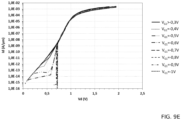
figures 9A ,9C et9E représentent des caractéristiques courant-tension du dispositif obtenues respectivement en augmentant une deuxième tension de grille VG2 et en fixant une première tension de grille VG1 à une valeur de -0.5V, en augmentant la première tension de grille VG1 et en fixant la deuxième tension de grille VG2 à une valeur de -0.5V, et en diminuant la deuxième tension de grille. - Les
figures 9B et 9D sont des tableaux récapitulant les paramètres appliqués lors des simulations desfigures 9A ,9C et9E .
- There
figure 1 represents an FDSOI transistor as known from the prior art. - THE
figures 2A And2B each represent the mapping of doping within the device according to one embodiment of the invention. - THE
figures 3A And3B represent current-voltage characteristics of the device according to one of the embodiments of the invention obtained by simulation. - There
Figure 3C is a table summarizing the parameters applied during the simulations of thefigures 3A And3B . - THE
Figures 4A and 4B represent the distribution of charges within the device respectively in a blocked configuration (V BG =1.7V) and in a passing configuration (V BG =1.8V). - There
Figure 4C is a table summarizing the parameters applied during the simulations of theFigures 4A and 4B . - THE
figures 5A And5B represent the distribution of the electrostatic potential within the device in blocked (V BG =1.7V) and on (V BG =1.8V) configurations. - There
Figure 5C is a table summarizing the parameters applied during the simulations of thefigures 5A And5B . - THE
Figures 6A and 6B represent simulations of the level of the conduction and valence bands of the device in blocked (V BG =1.7V) and on (V BG =1.8V) configurations. - There
Figure 6C is a table summarizing the parameters applied during the simulations of theFigures 6A and 6B . - THE
figures 7A And7B represent the distribution of the electric field in the direction of transport within the device in blocked (V BG =1.7V) and on (V BG =1.8V) configurations. - There
Figure 7C is a table summarizing the parameters applied during the simulations of thefigures 7A And7B . - THE
Figures 8A and 8B represent the distribution of the current density of the electrons within the device in blocked (V BG =1.7V) and on (V BG =1.8V) configurations. - There
Figure 8C is a table summarizing the parameters applied during the simulations of theFigures 8A and 8B . - THE
figures 9A ,9C And9E represent current-voltage characteristics of the device obtained respectively by increasing a second gate voltage V G2 and by setting a first gate voltage V G1 at a value of -0.5V, by increasing the first gate voltage V G1 and by setting the second gate voltage V G2 to a value of -0.5V, and decreasing the second gate voltage. - THE
Figures 9B and 9D are tables summarizing the parameters applied during the simulations of thefigures 9A ,9C And9E .
Les dessins sont donnés à titre d'exemples et ne sont pas limitatifs de l'invention. Ils constituent des représentations schématiques de principe destinées à faciliter la compréhension de l'invention et ne sont pas nécessairement à l'échelle des applications pratiques. En particulier les dimensions ne sont pas représentatives de la réalité.The drawings are given as examples and do not limit the invention. They constitute schematic representations of principle intended to facilitate the understanding of the invention and are not necessarily on the scale of practical applications. In particular, the dimensions are not representative of reality.
Avant d'entamer une revue détaillée de modes de réalisation de l'invention, sont énoncées ci-après des caractéristiques optionnelles qui peuvent éventuellement être utilisées en association ou alternativement :
Selon un exemple, le dispositif comprend en outre une première électrode et une deuxième électrode, la première zone dopée N est au contact de la première électrode qui est configurée pour recevoir une première tension de commande V110 et la première zone dopée P est au contact de la deuxième électrode qui est configurée pour recevoir une deuxième tension de commande V210.Before beginning a detailed review of embodiments of the invention, the following are set out as optional characteristics which may possibly be used in combination or alternatively:
According to one example, the device further comprises a first electrode and a second electrode, the first N-doped zone is in contact with the first electrode which is configured to receive a first control voltage V 110 and the first P-doped zone is in contact of the second electrode which is configured to receive a second control voltage V 210 .
Selon un exemple :
- La première tension de commande V110 constitue une tension de source VS du dispositif et la deuxième tension de commande V210 constitue une tension de drain VD du dispositif, ou
- La deuxième tension de commande V210 constitue la tension de source VS du dispositif et la première tension de commande V110 constitue la tension de drain VD du dispositif.
- The first control voltage V 110 constitutes a source voltage V S of the device and the second control voltage V 210 constitutes a drain voltage V D of the device, or
- The second control voltage V 210 constitutes the source voltage V S of the device and the first control voltage V 110 constitutes the drain voltage V D of the device.
Selon un exemple, le dispositif comprend en outre une première électrode de grille et une deuxième électrode de grille, la première grille est au contact de la première électrode de grille qui est configurée pour recevoir l'application d'une première tension de grille VG1 et la deuxième grille est au contact de la deuxième électrode de grille qui est configurée pour recevoir l'application d'une deuxième tension de grille VG2.According to one example, the device further comprises a first gate electrode and a second gate electrode, the first gate is in contact with the first gate electrode which is configured to receive the application of a first gate voltage V G1 and the second gate is in contact with the second gate electrode which is configured to receive the application of a second gate voltage V G2 .
Selon un exemple, le dispositif comprend une électrode de grille arrière et la grille arrière est au contact de l'électrode de grille arrière qui est configurée pour recevoir l'application d'une tension de grille arrière VBG.According to one example, the device comprises a rear gate electrode and the rear gate is in contact with the rear gate electrode which is configured to receive the application of a rear gate voltage V BG .
Selon un mode de réalisation, le dispositif comprend en outre un circuit de contrôle configuré pour appliquer :
- la première tension de commande V110 sur la première électrode,
- la deuxième tension de commande V210 sur la deuxième électrode,
- la première tension de grille VG1 sur la première électrode,
- la deuxième tension de grille VG2 sur la deuxième électrode,
- la tension de grille arrière VBG sur l'électrode de grille arrière,
- the first control voltage V 110 on the first electrode,
- the second control voltage V 210 on the second electrode,
- the first gate voltage V G1 on the first electrode,
- the second gate voltage V G2 on the second electrode,
- the rear gate voltage V BG on the rear gate electrode,
Selon un exemple, le circuit de contrôle est configuré pour pouvoir faire passer le dispositif d'une configuration passante, dans laquelle la jonction PN se trouve dans un état passant, à une configuration bloquée dans laquelle la jonction PN se trouve dans un état bloqué, ou inversement, ce en faisant varier la tension de grille arrière VBG entre une tension de grille arrière ouverte VBG,ON et une tension de grille arrière bloquée VBG,OFF distincte de la tension de grille arrière ouverte VBG,ON.According to one example, the control circuit is configured to be able to switch the device from a passing configuration, in which the PN junction is in a passing state, to a blocked configuration in which the PN junction is in a blocked state, or vice versa, by varying the rear gate voltage V BG between an open rear gate voltage V BG,ON and a blocked rear gate voltage V BG,OFF distinct from the open rear gate voltage V BG,ON .
Selon un exemple, VG1= VG2+ΔVG avec ΔVG compris entre -1V et +1V.According to an example, V G1 = V G2 +ΔV G with ΔV G between -1V and +1V.
Selon un exemple, VG1<0.According to an example, V G1 <0.
Selon un exemple, VG2<0.According to an example, V G2 <0.
Selon un exemple, VG1>0 et VG2>0.According to an example, V G1 >0 and V G2 >0.
Selon un exemple, VG1 = VG2.According to an example, V G1 = V G2 .
Selon un exemple, la jonction PN présente une tension de diffusion Vbi, et dans lequel la tension drain-source, définie par VD-VS, est supérieure à la tension de diffusion Vbi.According to one example, the PN junction has a diffusion voltage V bi , and in which the drain-source voltage, defined by V D -V S , is greater than the diffusion voltage V bi .
Selon un exemple, la tension de grille arrière VBG est comprise entre -1 et 2 V.According to one example, the rear gate voltage V BG is between -1 and 2 V.
Selon un exemple, le transistor n-MOS et le transistor p-MOS sont séparés d'une distance L supérieure à 10 nm, de préférence supérieure à 50nm, et/ou inférieure à 500 nm.According to one example, the n-MOS transistor and the p-MOS transistor are separated by a distance L greater than 10 nm, preferably greater than 50 nm, and/or less than 500 nm.
Un deuxième objet de l'invention concerne un procédé de contrôle du dispositif. Selon un exemple, le procédé prévoit de faire varier la tension de grille arrière VBG entre une tension de grille arrière ouverte VBG,ON et une tension de grille arrière bloquée VBG,OFF distincte de la tension de grille arrière ouverte VBG,ON, de sorte à faire passer le dispositif d'une configuration passante, dans laquelle la jonction PN se trouve dans un état passant, à une configuration bloquée dans laquelle la jonction PN se trouve dans un état bloqué.A second object of the invention relates to a method of controlling the device. According to one example, the method provides for varying the rear gate voltage V BG between an open rear gate voltage V BG, ON and a blocked rear gate voltage V BG, OFF distinct from the open rear gate voltage V BG, ON , so as to move the device from a passing configuration, in which the PN junction is in a passing state, to a blocked configuration in which the PN junction is in a blocked state.
Selon un exemple, le procédé prévoit l'application des tensions VG1 et VG2 de sorte que VG1= VG2+ΔVG avec ΔVG compris entre -1V et +1 V.According to one example, the method provides for the application of voltages V G1 and V G2 so that V G1 = V G2 +ΔV G with ΔV G between -1V and +1 V.
Selon un exemple, le procédé prévoit l'application des tensions VG1 et VG2 de sorte que VG1>0 et VG2>0.According to one example, the method provides for the application of voltages V G1 and V G2 so that V G1 >0 and V G2 >0.
Selon un exemple, le procédé prévoit l'application de la tension VG1 de sorte que VG1<0.According to one example, the method provides for the application of the voltage V G1 so that V G1 <0.
Selon un exemple, le procédé prévoit l'application de la tension VG2 de sorte que VG2<0.According to one example, the method provides for the application of the voltage V G2 so that V G2 <0.
Selon un exemple, le procédé prévoit l'application des tensions VG1 et VG2 de sorte que VG1 = VG2.According to one example, the method provides for the application of voltages V G1 and V G2 so that V G1 = V G2 .
Selon un exemple, le procédé prévoit l'application des tensions V110 et V210 de sorte que la tension drain-source, définie par VD-VS, soit supérieure à une tension de diffusion Vbi de la jonction PN.According to one example, the method provides for the application of voltages V 110 and V 210 so that the drain-source voltage, defined by V D -V S , is greater than a diffusion voltage V bi of the PN junction.
Selon un exemple, le procédé prévoit l'application d'une tension de grille arrière VBG comprise entre -1 et 2 V.According to one example, the method provides for the application of a rear gate voltage V BG of between -1 and 2 V.
Il est précisé que, dans le cadre de la présente invention, les termes « sur », « surmonte », « recouvre », « sous-jacent », en « vis-à-vis » et leurs équivalents ne signifient pas forcément « au contact de ». Ainsi par exemple, le dépôt, le report, le collage, l'assemblage ou l'application d'une première couche sur une deuxième couche, ne signifie pas obligatoirement que les deux couches sont directement au contact l'une de l'autre, mais signifie que la première couche recouvre au moins partiellement la deuxième couche en étant, soit directement à son contact, soit en étant séparée d'elle par au moins une autre couche ou au moins un autre élément.It is specified that, in the context of the present invention, the terms "on", "surmounts", "covers", "underlying", "vis-à-vis" and their equivalents do not necessarily mean "at the contact of”. For example, the deposition, transfer, gluing, assembly or application of a first layer on a second layer does not necessarily mean that the two layers are in direct contact with each other, but means that the first layer at least partially covers the second layer by being either directly in contact with it or by being separated from it by at least one other layer or at least one other element.
Une couche peut par ailleurs être composée de plusieurs sous-couches d'un même matériau ou de matériaux différents.A layer can also be composed of several sub-layers of the same material or of different materials.
On entend par un substrat, une couche, un dispositif, « à base » d'un matériau M, un substrat, une couche, un dispositif comprenant ce matériau M uniquement ou ce matériau M et éventuellement d'autres matériaux, par exemple des éléments d'alliage, des impuretés ou des éléments dopants. Ainsi un matériau à base d'un matériau III-N peut comprendre un matériau III-N additionné de dopants. De même, une couche à base de GaN comprend typiquement du GaN et des alliages d'AlGaN ou d'InGaN.By a substrate, a layer, a device, “based” on a material M, is meant a substrate, a layer, a device comprising this material M only or this material M and possibly other materials, for example elements alloy, impurities or doping elements. Thus a material based on a III-N material can comprise a III-N material with added dopants. Likewise, a GaN-based layer typically comprises GaN and AlGaN or InGaN alloys.
Le terme « matériau III-V » fait référence à un semi-conducteur composé d'un ou plusieurs éléments de la colonne III et de la colonne V du tableau périodique de Mendeleïev. On compte parmi les éléments de la colonne III le bore, le gallium, l'aluminium ou encore l'indium. La colonne V contient par exemple l'azote, l'arsenic, l'antimoine et le phosphore.The term "III-V material" refers to a semiconductor composed of one or more elements from column III and column V of the Mendeleev periodic table. The elements in column III include boron, gallium, aluminum and indium. Column V contains, for example, nitrogen, arsenic, antimony and phosphorus.
Un repère, de préférence orthonormé, comprenant les axes x, y, z est représenté en
Dans la présente demande de brevet, on parlera préférentiellement d'épaisseur pour une couche et de hauteur pour une structure ou un dispositif. L'épaisseur est prise selon une direction normale au plan d'extension principal de la couche, et la hauteur est prise perpendiculairement au plan de base XY. Ainsi, une couche présente typiquement une épaisseur selon z, lorsqu'elle s'étend principalement le long d'un plan XY, et un élément en saillie, par exemple une tranchée d'isolation, présente une hauteur selon z. Les termes relatifs « sur », « sous », « sous-jacent » se réfèrent préférentiellement à des positions prises selon la direction z.In this patent application, we will preferentially speak of thickness for a layer and height for a structure or a device. The thickness is taken in a direction normal to the main extension plane of the layer, and the height is taken perpendicular to the base plane XY. Thus, a layer typically has a thickness along z, when it extends mainly along a plane XY, and a projecting element, for example an insulation trench, has a height along z. Terms relative “on”, “under”, “underlying” refer preferentially to positions taken in the z direction.
Les termes « sensiblement », « environ », « de l'ordre de » signifient « à 10% près, de préférence à 5% près ».The terms “substantially”, “approximately”, “of the order of” mean “within 10%, preferably within 5%”.
Le dispositif selon différents modes de réalisation de l'invention va maintenant être décrit en référence aux
Le dispositif 1 comprend deux transistors à effet de champ : l'un du type n-MOS 100, et l'autre du type p-MOS 200. De préférence, il ne comprend pas d'autres transistors ou pour le moins pas d'autres transistors joints à l'un ou l'autre des deux premiers par une jonction PN.The
Le transistor n-MOS 100 comprend un premier drain, une première source, une première grille 101 et un premier oxyde de grille 102.The n-
Le premier oxyde de grille 102 s'étend sous la première grille 101. La première zone dopée N 110 et la deuxième zone dopée N 120 sont chacune en contact avec un premier canal 103, dit de conduction mais qui peut aussi être une zone désertée de porteurs, les séparant. Ce premier canal 103 est au contact de la face inférieure du premier oxyde de grille 102. Le premier canal 103 présente avantageusement une épaisseur selon la direction z comprise entre 5 et 10 nm, typiquement sensiblement égale à 7 nm.The
Le transistor n-MOS 100 comprend de plus typiquement des espaceurs 104 permettant d'isoler la première grille 101 du premier drain d'une part et de la première source d'autre part. Ces espaceurs 104 couvrent typiquement les flancs latéraux de la première grille 101. Ils sont entre autres destinés à limiter le couplage capacitif parasite entre la première grille 101 et la première source d'une part et le premier drain d'autre part.The n-
Le transistor p-MOS 200 comprend un deuxième drain, une deuxième source, une deuxième grille 201, un deuxième oxyde de grille 202 et un deuxième canal 203 lui aussi dit de conduction mais pouvant aussi être une zone désertée de porteurs. Les caractéristiques du transistor n-MOS 100 peuvent être transposées mutatis mutandis au transistor p-MOS 200.The p-
Le transistor n-MOS 100 et le transistor p-MOS 200 sont séparés d'une distance L mesurée dans le plan XY et définie comme la distance entre un flanc 106 du transistor n-MOS 100 et un flanc 206 du transistor p-MOS 200 lui faisant face. Les flancs 106, 206 des transistors 100, 200 correspondent typiquement aux flancs des espaceurs 104, 204. La distance L est de préférence, pour des raisons de limitations technologiques lors de la fabrication du dispositif, supérieure à 50 nm. Il serait cependant envisageable dans les applications visées que la distance L soit fixée à des valeurs aussi faibles que 10 nm. Dans un objectif d'optimisation de la densité de dispositifs pouvant être intégrés sur une puce, elle est de préférence inférieure à 500 nm.The n-
Le dispositif comprend de plus une première zone dopée N 110 et une deuxième zone dopée N 120. La première zone dopée N 110 et la deuxième zone dopée N 120 peuvent constituer respectivement le premier drain et la première source, ou inversement.The device further comprises a first N-doped
De manière similaire, le dispositif comprend une première zone dopée P 210 et une deuxième zone dopée P 220 pouvant constituer respectivement le deuxième drain et la deuxième source, ou inversement.Similarly, the device comprises a first P-doped
La deuxième zone dopée N 120 et la deuxième zone dopée P 220 sont en contact et forment ainsi une jonction PN 1000. La jonction PN 1000 présente une tension de diffusion, couramment désignée par le terme anglais de tension de « built-in », notée VBI et dont la valeur dépend notamment du niveau de dopage des zones 120, 220 la constituant.The
Les zones dopées 110, 120, 210, 220 se trouvent de préférence toutes dans une couche active 10. La couche active 10 est de préférence à base d'au moins un matériau IV-IV. Il peut également être à base d'au moins un matériau III-V, de préférence à base d'au moins un matériau III-N. Par exemple, ce matériau est à base de GaN. Ce matériau peut également être à base de silicium. Il peut s'agir d'une couche homogène, formée typiquement d'un unique matériau. La couche active 10 présente typiquement une face supérieure 11 et une face inférieure 12 s'étendant toutes les deux principalement dans le plan XY du repère orthogonal XYZ. Elle présente selon la direction z une épaisseur e10. L'épaisseur e10 de la couche active 10 est avantageusement comprise entre 20 et 30 nm, typiquement sensiblement égale à 25 nm.The doped
Certains éléments constituant les transistors 100, 200 peuvent avoir été au moins partiellement formés à partir d'une couche continue dite couche de fabrication. Par exemple, certaines régions de la couche de fabrication auront pu être oxydées pour former les oxydes de grille 102, 202 et/ou les espaceurs 104, 204. La couche de fabrication peut également avoir été gravée puis différents dépôts auront pu être réalisés sur cette couche de fabrication afin de former les oxydes de grille 102, 202, espaceurs 104, 204 et/ou grilles 101, 201. Les régions non transformées ou gravées de la couche de fabrication font alors partie de la couche active 10. La couche active 10 peut de plus comprendre des zones ayant été épitaxiées à partir de la couche de fabrication.Certain elements constituting the
Afin de réaliser une jonction PN 1000 fonctionnelle, dans le cas où la deuxième zone dopée N 120 constitue le premier drain, la deuxième zone dopée P 220 constitue la deuxième source. En conséquence, la première zone dopée N 110 constitue alors la première source et la première zone dopée P 220 constitue le deuxième drain. Dans ce cas de figure, la première zone dopée N 110 constitue la source et la première zone dopée P 220 le drain du dispositif 1.In order to produce a
A l'inverse, dans le cas où la deuxième zone dopée N 120 constitue la première source, la deuxième zone dopée P 220 constitue le deuxième drain. En conséquence, la première zone dopée N 110 constitue alors le premier drain et la première zone dopée P 220 constitue la deuxième source. Dans ce cas de figure, la première zone dopée N 110 constitue le drain et la première zone dopée P 220 la source du dispositif 1.Conversely, in the case where the second N-doped
Le dispositif 1 comprend de plus une couche diélectrique 300 présentant une face supérieure 301 et une face inférieure 302 s'étendant toutes les deux principalement dans des plans parallèles au plan XY du repère orthogonal. La face supérieure 301 de la couche diélectrique 300 se trouve au contact de la première zone dopée N 110, de la deuxième zone dopée N 120, de la première zone dopée P 210 et de la deuxième zone dopée P 220. La couche diélectrique 300 constitue ainsi un diélectrique enterré commun aux deux transistors 100, 200 et donc de façon générale un diélectrique enterré pour le dispositif 1. Elle présente selon la direction z une épaisseur e300 typiquement égale à 25 nm. Cette valeur correspond aux standards de l'industrie microélectronique. L'invention peut cependant parfaitement fonctionner pour d'autres valeurs de e300. La valeur de la tension de grille arrière VBG sera ajustée en fonction de la valeur de e300 : plus la couche diélectrique 300 sera épaisse, plus la tension de grille arrière à appliquer sera élevée.The
Le dispositif 1 comprend en outre une grille arrière 400 au contact de la face inférieure 302 de la couche diélectrique 300.The
Le dispositif 1 peut comprendre les électrodes ou reprises de contact suivantes :
- une première électrode 115 au contact de la première
zone dopée N 110, - une deuxième électrode 215 au contact de la première
zone dopée P 210, - une première électrode de
grille 105 au contact de la premièregrille 101, - une deuxième électrode de
grille 205 au contact de la deuxièmegrille 201, - une électrode de grille arrière 405 au contact de la
grille arrière 400,
- a
first electrode 115 in contact with the first N-dopedzone 110, - a
second electrode 215 in contact with the first P-dopedzone 210, - a
first gate electrode 105 in contact with thefirst gate 101, - a
second gate electrode 205 in contact with thesecond gate 201, - a
rear gate electrode 405 in contact with therear gate 400,
Plus précisément, on prévoit notamment que puissent être appliquées :
- une première tension de commande V110 sur la première électrode 115,
- une deuxième tension de commande V210 sur la deuxième électrode 215,
- une première tension de grille VG1 sur la première électrode 105,
- une deuxième tension de grille VG2 sur la deuxième électrode 205,
- une tension de grille arrière VBG sur l'électrode de
grille arrière 405.
- a first control voltage V 110 on the
first electrode 115, - a second control voltage V 210 on the
second electrode 215, - a first gate voltage V G1 on the
first electrode 105, - a second gate voltage V G2 on the
second electrode 205, - a rear gate voltage V BG on the
rear gate electrode 405.
De préférence, toutes les électrodes 115, 215, 105, 205 et 405 sont accessibles - c'est-à-dire que des tensions peuvent leur être appliquées -depuis une même face dite face avant du dispositif 1. Dans cette optique, la grille arrière 400 fait avantageusement saillie par rapport à la couche diélectrique 300 de sorte à permettre une reprise de contact de ladite grille arrière 400 depuis la face avant du dispositif 1. La couche diélectrique 300 peut en outre, au niveau de cette reprise de contact, présenter une surépaisseur. Cette surépaisseur correspond typiquement à la somme de l'épaisseur e300 de la couche diélectrique 300 et de l'épaisseur e10 de la couche active 10. L'électrode de grille arrière 405 se trouve alors de niveau selon la direction z avec la première électrode 115 et la deuxième électrode 215. Cela permet de faciliter leur fabrication simultanée. On prévoit alors avantageusement la présence d'au moins une tranchée d'isolation peu profonde (couramment désignée STI, acronyme anglais de « Shallow Trench Isolation ») permettant d'isoler électriquement la grille arrière 400 de la couche active 10.Preferably, all the
Ainsi, le comportement du dispositif 1 peut être contrôlé au niveau de cinq points de commande. Les transistors FDSOI, couramment utilisés dans l'industrie microélectronique, qui présentent une unique grille en face avant, ne peuvent être contrôlés qu'au niveau de quatre points de commande (drain, source, grille avant, grille arrière, visibles sur la
La première tension de commande V110 et la deuxième tension de commande V210 constituent pour le dispositif 1 respectivement une tension de drain VD et une tension de source VS, ou inversement. Plus précisément :
- Si la première
zone dopée N 110 constitue la première source et la premièrezone dopée P 210 le deuxième drain, alors la première tension de commande V110 constitue la tension de source VS du dispositif 1 et la deuxième tension de commande V210 constitue la tension de drain VD du dispositif 1. Ce cas de figure est envisagé à lafigure 2A . - Si la première
zone dopée N 110 constitue le premier drain et la premièrezone dopée P 210 la deuxième source, alors la première tension de commande V110 constitue la tension de drain VD du dispositif 1 et la deuxième tension de commande V210 constitue la tension de source VS du dispositif 1. Ce cas de figure est envisagé à lafigure 2B .
- If the first N-doped
zone 110 constitutes the first source and the first P-dopedzone 210 the second drain, then the first control voltage V 110 constitutes the source voltage V S of thedevice 1 and the second control voltage V 210 constitutes the drain voltage V D ofdevice 1. This scenario is considered in theFigure 2A . - If the first N-doped
zone 110 constitutes the first drain and the first P-dopedzone 210 the second source, then the first control voltage V 110 constitutes the drain voltage V D ofdevice 1 and the second control voltage V 210 constitutes the source voltage V S ofdevice 1. This scenario is considered at theFigure 2B .
Dans le premier cas de figure, la source du dispositif 1 se trouve au niveau d'une zone dopée N et le drain au niveau d'une zone dopée P. Dans cette configuration, le dispositif 1 en fonctionnement aura donc un comportement global de type n-MOS. A l'inverse, dans le second cas de figure, la source du dispositif 1 se trouve au niveau d'une zone dopée P et le drain au niveau d'une source dopée N. Le dispositif 1 en fonctionnement aura donc cette fois un comportement global de type p-MOS.In the first case, the source of
Il est à noter que la fonction de source ou de drain des zones 110, 120, 210 et 220 dépend des tensions qui leur sont appliquées, et plus exactement du signe des tensions V110-V120 et V210-V220. Ainsi, il est possible de faire passer le dispositif 1 d'un comportement n-MOS à un comportement p-MOS, et inversement, en changeant simplement le signe de ces différences de tension. Le dispositif 1 constitue ainsi un dispositif à commutation vertical (souvent désigné par le terme anglais de « sharp switch device »).It should be noted that the source or drain function of
La tension de grille arrière joue, elle, dans le dispositif 1, un rôle majeur de commande.The rear gate voltage plays a major control role in
Le dispositif 1 en fonctionnement peut se trouver dans une configuration dite passante ou dans une configuration dite bloquée.The
Dans la configuration bloquée, la jonction PN 1000 se trouve dans un état bloqué. Elle présente une zone de charge d'espace, ou zone de déplétion, comprenant des charges fixes mais dans laquelle les charges libres ne peuvent pas circuler. Une barrière de potentiel sépare ainsi le transistor n-MOS 100 et le transistor p-MOS 200 et empêche la circulation du courant entre la source et le drain du dispositif 1. Cette configuration bloquée du dispositif 1 peut également être appelée « état OFF » du dispositif 1.In the blocked configuration, the
Dans la configuration passante du dispositif 1, la jonction PN 1000 se trouve dans un état passant. Il n'y a donc pas de barrière de potentiel entre le transistor n-MOS 100 et le transistor p-MOS 200. En conséquence, l'ensemble formé par le premier canal de conduction 103, la jonction PN 1000 et le deuxième canal de conduction 203 est traversé par des charges circulant librement entre la source et le drain du dispositif. Le courant peut donc circuler dans le dispositif 1. Cette configuration passante du dispositif 1 peut être désignée « état ON » du dispositif 1.In the conducting configuration of
Le passage de la configuration bloquée à la configuration passante du dispositif 1, ou inversement, se fait par commutation de la jonction PN 1000. Une telle jonction se caractérise notamment par sa rapidité de commutation, ce qui confère au dispositif 1 lui-même une excellente efficacité de passage de l'état ON à l'état OFF et inversement. C'est ce qui va par la suite être caractérisé en référence aux
Le fait qu'une faible variation de tension permette de faire passer le dispositif d'un état à l'autre permet de garantir une forte efficacité énergétique. Le dispositif 1 peut donc être utilisé dans des applications électroniques de très faible consommation énergétique. Cela permet de plus d'améliorer ses performances en termes de rapidité de réponse à une sollicitation extérieure. Cette caractéristique est ainsi à l'origine de plusieurs avantages importants du dispositif 1.The fact that a small variation in voltage makes it possible to pass the device from one state to another guarantees high energy efficiency.
Toutes les simulations présentées dans les
Les
- la première tension de grille VG1 et la deuxième tension de grille VG2 ont été fixées à une même valeur positive. La simulation a été réalisées pour plusieurs valeurs de VG1=VG2, variant de -1V à 0V. Ces différentes simulations correspondent aux différentes courbes sur les
figures 3A et3B . - la tension drain-source VDS a été fixée à une valeur de 1V. Cette valeur est notamment supérieure à la tension de built-in, ou tension de diffusion, de la jonction
PN 1000. - la tension de grille arrière VBG varie de -1V à 2V.
- on relève l'évolution du courant de drain-source IDS circulant dans le dispositif 1 en fonction de VBG.
- the first gate voltage V G1 and the second gate voltage V G2 have been fixed at the same positive value. The simulation was carried out for several values of V G1 =V G2 , varying from -1V to 0V. These different simulations correspond to the different curves on the
figures 3A And3B . - the drain-source voltage V DS was fixed at a value of 1V. This value is notably higher than the built-in voltage, or diffusion voltage, of the
PN 1000 junction. - the rear gate voltage V BG varies from -1V to 2V.
- we note the evolution of the drain-source current I DS circulating in the
device 1 as a function of V BG .
Ces éléments sont récapitulés dans le tableau présenté en
Ces figures témoignent d'une commutation abrupte du courant (comportement parfois désigné par le terme anglais « steep slope », pouvant être traduit par « pente raide »). Une variation de la tension de grille arrière VBG de quelques mV (1mV=10-3V) seulement permet une variation de jusqu'à huit décades de courant. Cela correspond à une pente sous le seuil pouvant des valeurs aussi faibles que 1mV/dec. A titre de comparaison, la pente sous le seuil des transistors FDSOI couramment utilisés dans l'industrie est généralement de l'ordre de 80mV/dec. Le dispositif 1 selon l'invention permet donc d'atteindre des performances bien supérieures aux transistors FDSOI classiques.These figures demonstrate an abrupt switching of the current (behavior sometimes referred to by the English term “steep slope”, which can be translated as “steep slope”). A variation of the rear gate voltage V BG of only a few mV (1mV=10 -3 V) allows a variation of up to eight decades of current. This corresponds to a slope below the threshold which can have values as low as 1mV/dec. For comparison, the subthreshold slope of FDSOI transistors commonly used in industry is generally around 80mV/dec. The
Par exemple, pour VG1=VG2=-0,9V, une variation d'un courant d'environ 10-5A à un courant d'environ 10-13A est obtenue pour une variation de VBG de moins de 50mV.For example, for V G1 =V G2 =-0.9V, a variation from a current of approximately 10 -5 A to a current of approximately 10 -13 A is obtained for a variation of V BG of less than 50mV .
Il est à noter que la tension de grille arrière à laquelle le dispositif 1 commute VBG,commutation peut être réglée sur une large plage de tension, ici d'environ -0,5V à près de 1,5V, en ajustant la tension appliquée sur la première grille 101 et la deuxième grille 201. Ainsi, le dispositif 1 peut être utilisé pour différentes applications par simple paramétrage des tensions VG1 et VG2.It should be noted that the rear gate voltage at which
Les
Au cours de cette simulation :
- la première tension de grille VG1 et la deuxième tension de grille VG2 ont été fixées à une même valeur de -1V.
- la tension drain-source VDS a été fixée à une valeur de 1V.
- la tension de grille arrière VBG est fixée une première fois à 1,7V (
figure 4A ) et une fois à 1,8V (figure 4B ). - on relève la densité de charge volumique, exprimée en C.m-3, en tout point du dispositif.
- the first gate voltage V G1 and the second gate voltage V G2 were fixed at the same value of -1V.
- the drain-source voltage V DS was fixed at a value of 1V.
- the rear gate voltage V BG is first set at 1.7V (
Figure 4A ) and once at 1.8V (Figure 4B ). - the volume charge density is recorded, expressed in Cm -3 , at any point of the device.
Ces éléments sont récapitulés dans le tableau présenté en
Ces cartographies permettent notamment d'observer l'évolution de la zone de charge d'espace de la jonction PN 1000. On observe que celle-ci crée une barrière de potentiel sur toute la hauteur de la jonction lorsque VBG=1,7V (
Les
Il est à noter que les
Les
Les
Les
Les caractéristiques venant d'être étudiées en référence aux
Tout d'abord, la
Au cours de cette simulation :
- la première tension de grille VG1 est fixée à -0,5V.
- la tension drain-source VDS varie de 0V à 2V.
- la tension de grille arrière VBG a été fixée à 0,4V.
- on relève l'évolution du courant de drain-source IDS circulant dans le dispositif 1 en fonction de VDS et ce pour différentes valeurs de VG2 comprises entre -1V et 1V correspondant à autant de courbe sur la
figure 9A .
- the first gate voltage V G1 is set to -0.5V.
- the drain-source voltage V DS varies from 0V to 2V.
- the rear gate voltage V BG was set to 0.4V.
- we note the evolution of the drain-source current I DS circulating in the
device 1 as a function of V DS and this for different values of V G2 between -1V and 1V corresponding to as many curves on theFigure 9A .
On observe qu'une commutation abrupte du courant drain-source IDS est obtenue autour d'une tension de commutation VDS,commutation=1.05V, et ce quelle que soit la tension VG2 appliquée sur la grille du transistor p-MOS.We observe that an abrupt switching of the drain-source current I DS is obtained around a switching voltage V DS, switching = 1.05V, whatever the voltage V G2 applied to the gate of the p-MOS transistor.
La
- la deuxième tension de grille VG2 est fixée à -0,5V.
- la tension drain-source VDS varie de 0V à 2V.
- la tension de grille arrière VBG a été fixée à 0,4V.
- on relève l'évolution du courant de drain-source IDS circulant dans le dispositif 1 en fonction de VDS et ce pour différentes valeurs de VG1 comprises entre -1V et 1V correspondant à autant de courbe sur la
figure 9C .
- the second gate voltage V G2 is set to -0.5V.
- the drain-source voltage V DS varies from 0V to 2V.
- the rear gate voltage V BG was set to 0.4V.
- we note the evolution of the drain-source current I DS circulating in the
device 1 as a function of V DS and this for different values of V G1 between -1V and 1V corresponding to as many curves on theFigure 9C .
On observe qu'une commutation abrupte du courant drain-source IDS est obtenue à la condition que la première tension de grille VG1 se trouve dans la bonne plage de valeurs. Dans le cas présent, il faut que VG1<-0,3V. En dessus de ce seuil, i.e. pour VG1>-0,3V, la première tension de grille n'est pas suffisante pour former la barrière de potentiel au niveau de la jonction PN 1000 entre le drain du transistor n-MOS 100 et la source du transistor p-MOS 200. Le dispositif 1 ne présente alors pas de commutation abrupte et a un comportement semblable à celui d'une diode PIN. Pour VG1<-0,3V, la première tension de grille est suffisante pour former la barrière de potentiel au niveau de la jonction PN 1000. Une commutation abrupte est observée et a lieu pour une tension drain-source VDS d'autant plus forte que la première tension de grille VG1 est faible. En effet, plus VG1 est faible, plus la barrière de potentiel est grande, plus la tension drain-source nécessaire à la faire disparaître est élevée et donc plus la tension de commutation VDS,commutation est élevée.It is observed that an abrupt switching of the drain-source current I DS is obtained on the condition that the first gate voltage V G1 is in the correct range of values. In this case, V G1 must <-0.3V. Above this threshold, ie for V G1 >-0.3V, the first gate voltage is not sufficient to form the potential barrier at the
La
On remarque que, pour chacune des valeurs de première tension de grille VG1 étudiée, la tension de commutation VDS,commutation est différente en mode « backward » et en mode « forward ». La tension de commutation VDS,commutation,BW en mode backward est notamment ici inférieure à la tension de commutation VDS,commutation,FW en mode forward. Ces deux figures mettent donc en évidence un phénomène d'hystérésis, qui peut être mis à profit dans des applications mémoires.We note that, for each of the values of first gate voltage V G1 studied, the switching voltage V DS, switching is different in “backward” mode and in “forward” mode. The switching voltage V DS, switching, BW in backward mode is notably lower here than the switching voltage V DS, switching, FW in forward mode. These two figures therefore highlight a hysteresis phenomenon, which can be taken advantage of in memory applications.
Selon un mode de réalisation, le dispositif 1 comprend un circuit de contrôle permettant d'appliquer les tensions précédemment mentionnées sur chacune de ces électrodes. Le circuit de contrôle permet en outre de faire varier les tensions V110, V210, VG1, VG2 et VBG, par exemple dans une plage donnée telle que [-5V, 5V].According to one embodiment, the
Le circuit de contrôle est avantageusement configuré pour pouvoir faire passer le dispositif 1 de la configuration passante à la configuration bloquée et inversement.The control circuit is advantageously configured to be able to switch the
L'invention n'est pas limitée aux modes de réalisations précédemment décrits et s'étend à tous les modes de réalisation couverts par l'invention.The invention is not limited to the embodiments previously described and extends to all the embodiments covered by the invention.
Claims (17)
Applications Claiming Priority (1)
| Application Number | Priority Date | Filing Date | Title |
|---|---|---|---|
| FR2206178A FR3137209A1 (en) | 2022-06-22 | 2022-06-22 | Microelectronic device with two field effect transistors |
Publications (1)
| Publication Number | Publication Date |
|---|---|
| EP4297090A1 true EP4297090A1 (en) | 2023-12-27 |
Family
ID=83505774
Family Applications (1)
| Application Number | Title | Priority Date | Filing Date |
|---|---|---|---|
| EP23180759.5A Pending EP4297090A1 (en) | 2022-06-22 | 2023-06-21 | Microelectronic device with two field effect transistors |
Country Status (3)
| Country | Link |
|---|---|
| US (1) | US20240030221A1 (en) |
| EP (1) | EP4297090A1 (en) |
| FR (1) | FR3137209A1 (en) |
Citations (4)
| Publication number | Priority date | Publication date | Assignee | Title |
|---|---|---|---|---|
| WO2007109658A2 (en) * | 2006-03-20 | 2007-09-27 | Rochester Institute Of Technology | Shared metallic source/drain cmos circuits and methods thereof |
| KR20110105826A (en) * | 2009-01-19 | 2011-09-27 | 가부시키가이샤 히타치세이사쿠쇼 | Semiconductor device, method for manufacturing same, and semiconductor storage device |
| US20140167167A1 (en) * | 2012-12-14 | 2014-06-19 | Stmicroelectronics Sa | Cmos cell produced in fd-soi technology |
| WO2021050194A1 (en) * | 2019-09-11 | 2021-03-18 | The Penn State Research Foundation | Gaussian synapses for probabilistic neural networks |
-
2022
- 2022-06-22 FR FR2206178A patent/FR3137209A1/en active Pending
-
2023
- 2023-06-21 EP EP23180759.5A patent/EP4297090A1/en active Pending
- 2023-06-22 US US18/339,319 patent/US20240030221A1/en active Pending
Patent Citations (4)
| Publication number | Priority date | Publication date | Assignee | Title |
|---|---|---|---|---|
| WO2007109658A2 (en) * | 2006-03-20 | 2007-09-27 | Rochester Institute Of Technology | Shared metallic source/drain cmos circuits and methods thereof |
| KR20110105826A (en) * | 2009-01-19 | 2011-09-27 | 가부시키가이샤 히타치세이사쿠쇼 | Semiconductor device, method for manufacturing same, and semiconductor storage device |
| US20140167167A1 (en) * | 2012-12-14 | 2014-06-19 | Stmicroelectronics Sa | Cmos cell produced in fd-soi technology |
| WO2021050194A1 (en) * | 2019-09-11 | 2021-03-18 | The Penn State Research Foundation | Gaussian synapses for probabilistic neural networks |
Also Published As
| Publication number | Publication date |
|---|---|
| FR3137209A1 (en) | 2023-12-29 |
| US20240030221A1 (en) | 2024-01-25 |
Similar Documents
| Publication | Publication Date | Title |
|---|---|---|
| EP2685500A1 (en) | Integrated circuit on SOI comprising a thyristor (SCR) protecting against electrostatic discharges | |
| FR2558010A1 (en) | PROCESS FOR THE MANUFACTURE OF COMPLEMENTARY MOS TRANSISTORS WITH LOW THRESHOLD VOLTAGES IN INTEGRATED HIGH DENSITY CIRCUITS AND STRUCTURE RESULTING THEREFROM | |
| FR2980035A1 (en) | INTEGRATED CIRCUIT IN SELF COMPRISING ADJACENT CELLS OF DIFFERENT TYPES | |
| FR3005203A1 (en) | INTEGRATED SINGLE CIRCUIT COMPRISING A PROTECTION TRANSISTOR AGAINST ELECTROSTATIC DISCHARGES | |
| EP2415079A1 (en) | Self-contained integrated circuit having transistors with separate threshold voltages | |
| EP2685499A1 (en) | SOI integrated circuit comprising a triac for protection against electrostatic discharges | |
| EP2685501A1 (en) | SOI integrated circuit comprising an underlying protection transistor | |
| EP0581625B1 (en) | Multifunctional electronic device, in particular element with a negative dynamic resistance and corresponding method of fabrication | |
| FR3003996A1 (en) | METHOD FOR CONTROLLING AN INTEGRATED CIRCUIT | |
| EP2835825A1 (en) | SOI integrated circuit provided with a device for protection against electrostatic discharges | |
| EP0543745B1 (en) | MOS transistor with integrated zener diode protection | |
| FR3038775A1 (en) | SUBSTRATE CONTACT PLUG FOR A MOS TRANSISTOR IN A SOIL SUBSTRATE, ESPECIALLY FDSOI | |
| FR3033938A1 (en) | ZENER DIODE WITH ADJUSTABLE CLAMPING VOLTAGE | |
| FR2984607A1 (en) | CURED PHOTODIODE IMAGE SENSOR | |
| EP2775529A2 (en) | Tunnel-effect transistor | |
| FR2981503A1 (en) | TRANSISTOR MOS NOT SUBJECT TO HUMP EFFECT | |
| EP2685502A1 (en) | SOI integrated circuit comprising a bipolar transistor with insulating trenches of different depths | |
| EP2947689B1 (en) | Photonic cmos inverter | |
| EP2750179B1 (en) | Integrated circuit including a clock tree cell | |
| FR3095891A1 (en) | Electric circuit | |
| FR2996956A1 (en) | INTEGRATED CIRCUIT HAVING TRANSISTORS WITH DIFFERENT THRESHOLD VOLTAGES | |
| EP4297090A1 (en) | Microelectronic device with two field effect transistors | |
| FR2911007A1 (en) | Image sensor pixel, has accessing zones for crossing layer which forms caissons and extending until in buried semiconductor layer, and insulation zones strongly doped than layer forming caissons and edging source zones | |
| EP3772093A1 (en) | Manufacturing method comprising definition of an effective length of mosfet transistor channel | |
| EP1107314A1 (en) | Radiation hardened MOS transistors |
Legal Events
| Date | Code | Title | Description |
|---|---|---|---|
| PUAI | Public reference made under article 153(3) epc to a published international application that has entered the european phase |
Free format text: ORIGINAL CODE: 0009012 |
|
| STAA | Information on the status of an ep patent application or granted ep patent |
Free format text: STATUS: REQUEST FOR EXAMINATION WAS MADE |
|
| 17P | Request for examination filed |
Effective date: 20230621 |
|
| AK | Designated contracting states |
Kind code of ref document: A1 Designated state(s): AL AT BE BG CH CY CZ DE DK EE ES FI FR GB GR HR HU IE IS IT LI LT LU LV MC ME MK MT NL NO PL PT RO RS SE SI SK SM TR |
|
| RAP3 | Party data changed (applicant data changed or rights of an application transferred) |
Owner name: COMMISSARIAT A L'ENERGIE ATOMIQUE ET AUX ENERGIESALTERNATIVES |