EP2947689B1 - Photonic cmos inverter - Google Patents
Photonic cmos inverter Download PDFInfo
- Publication number
- EP2947689B1 EP2947689B1 EP15168852.0A EP15168852A EP2947689B1 EP 2947689 B1 EP2947689 B1 EP 2947689B1 EP 15168852 A EP15168852 A EP 15168852A EP 2947689 B1 EP2947689 B1 EP 2947689B1
- Authority
- EP
- European Patent Office
- Prior art keywords
- transistor
- zone
- junction
- photosensitive
- logic
- Prior art date
- Legal status (The legal status is an assumption and is not a legal conclusion. Google has not performed a legal analysis and makes no representation as to the accuracy of the status listed.)
- Active
Links
- 238000005286 illumination Methods 0.000 claims description 39
- 239000004065 semiconductor Substances 0.000 claims description 31
- 230000006870 function Effects 0.000 claims description 29
- 239000000758 substrate Substances 0.000 claims description 19
- 230000005855 radiation Effects 0.000 claims description 16
- 230000008878 coupling Effects 0.000 claims description 9
- 238000010168 coupling process Methods 0.000 claims description 9
- 238000005859 coupling reaction Methods 0.000 claims description 9
- 239000012212 insulator Substances 0.000 claims description 9
- 239000002800 charge carrier Substances 0.000 claims description 3
- 239000010410 layer Substances 0.000 description 58
- 230000010287 polarization Effects 0.000 description 21
- 238000005513 bias potential Methods 0.000 description 16
- CIWBSHSKHKDKBQ-JLAZNSOCSA-N Ascorbic acid Chemical compound OC[C@H](O)[C@H]1OC(=O)C(O)=C1O CIWBSHSKHKDKBQ-JLAZNSOCSA-N 0.000 description 9
- 230000008859 change Effects 0.000 description 8
- 230000007423 decrease Effects 0.000 description 7
- 238000005516 engineering process Methods 0.000 description 7
- 238000009825 accumulation Methods 0.000 description 6
- 238000002513 implantation Methods 0.000 description 6
- 229910052757 nitrogen Inorganic materials 0.000 description 5
- 229910052698 phosphorus Inorganic materials 0.000 description 5
- 229910004298 SiO 2 Inorganic materials 0.000 description 4
- 125000006850 spacer group Chemical group 0.000 description 4
- 229910000577 Silicon-germanium Inorganic materials 0.000 description 3
- 238000000137 annealing Methods 0.000 description 3
- 239000004020 conductor Substances 0.000 description 3
- 230000001419 dependent effect Effects 0.000 description 3
- 238000010292 electrical insulation Methods 0.000 description 3
- 239000000463 material Substances 0.000 description 3
- 239000011159 matrix material Substances 0.000 description 3
- 229910052710 silicon Inorganic materials 0.000 description 3
- 239000010703 silicon Substances 0.000 description 3
- 230000007704 transition Effects 0.000 description 3
- OAICVXFJPJFONN-UHFFFAOYSA-N Phosphorus Chemical compound [P] OAICVXFJPJFONN-UHFFFAOYSA-N 0.000 description 2
- 241001080024 Telles Species 0.000 description 2
- 229910052785 arsenic Inorganic materials 0.000 description 2
- 230000003247 decreasing effect Effects 0.000 description 2
- 230000007547 defect Effects 0.000 description 2
- 238000001514 detection method Methods 0.000 description 2
- 239000003989 dielectric material Substances 0.000 description 2
- 230000000694 effects Effects 0.000 description 2
- 229910052738 indium Inorganic materials 0.000 description 2
- APFVFJFRJDLVQX-UHFFFAOYSA-N indium atom Chemical compound [In] APFVFJFRJDLVQX-UHFFFAOYSA-N 0.000 description 2
- 230000000284 resting effect Effects 0.000 description 2
- ZOXJGFHDIHLPTG-UHFFFAOYSA-N Boron Chemical compound [B] ZOXJGFHDIHLPTG-UHFFFAOYSA-N 0.000 description 1
- 229910000530 Gallium indium arsenide Inorganic materials 0.000 description 1
- 238000004026 adhesive bonding Methods 0.000 description 1
- RQNWIZPPADIBDY-UHFFFAOYSA-N arsenic atom Chemical compound [As] RQNWIZPPADIBDY-UHFFFAOYSA-N 0.000 description 1
- 230000001174 ascending effect Effects 0.000 description 1
- 229910052796 boron Inorganic materials 0.000 description 1
- 239000000969 carrier Substances 0.000 description 1
- 230000001808 coupling effect Effects 0.000 description 1
- 230000023077 detection of light stimulus Effects 0.000 description 1
- 238000009792 diffusion process Methods 0.000 description 1
- 235000021183 entrée Nutrition 0.000 description 1
- 238000000407 epitaxy Methods 0.000 description 1
- 230000002349 favourable effect Effects 0.000 description 1
- 238000011065 in-situ storage Methods 0.000 description 1
- 238000009413 insulation Methods 0.000 description 1
- 238000005468 ion implantation Methods 0.000 description 1
- 238000002955 isolation Methods 0.000 description 1
- 230000000670 limiting effect Effects 0.000 description 1
- 229910044991 metal oxide Inorganic materials 0.000 description 1
- 150000004706 metal oxides Chemical class 0.000 description 1
- 238000004377 microelectronic Methods 0.000 description 1
- -1 or Ge Inorganic materials 0.000 description 1
- 239000011574 phosphorus Substances 0.000 description 1
- 230000008439 repair process Effects 0.000 description 1
- 230000002441 reversible effect Effects 0.000 description 1
- 230000000630 rising effect Effects 0.000 description 1
- 238000000926 separation method Methods 0.000 description 1
- 241000894007 species Species 0.000 description 1
- 230000003068 static effect Effects 0.000 description 1
- 239000002344 surface layer Substances 0.000 description 1
- 229910052720 vanadium Inorganic materials 0.000 description 1
Images


Classifications
-
- G—PHYSICS
- G02—OPTICS
- G02F—OPTICAL DEVICES OR ARRANGEMENTS FOR THE CONTROL OF LIGHT BY MODIFICATION OF THE OPTICAL PROPERTIES OF THE MEDIA OF THE ELEMENTS INVOLVED THEREIN; NON-LINEAR OPTICS; FREQUENCY-CHANGING OF LIGHT; OPTICAL LOGIC ELEMENTS; OPTICAL ANALOGUE/DIGITAL CONVERTERS
- G02F3/00—Optical logic elements; Optical bistable devices
- G02F3/02—Optical bistable devices
-
- H—ELECTRICITY
- H01—ELECTRIC ELEMENTS
- H01L—SEMICONDUCTOR DEVICES NOT COVERED BY CLASS H10
- H01L27/00—Devices consisting of a plurality of semiconductor or other solid-state components formed in or on a common substrate
- H01L27/02—Devices consisting of a plurality of semiconductor or other solid-state components formed in or on a common substrate including semiconductor components specially adapted for rectifying, oscillating, amplifying or switching and having at least one potential-jump barrier or surface barrier; including integrated passive circuit elements with at least one potential-jump barrier or surface barrier
- H01L27/04—Devices consisting of a plurality of semiconductor or other solid-state components formed in or on a common substrate including semiconductor components specially adapted for rectifying, oscillating, amplifying or switching and having at least one potential-jump barrier or surface barrier; including integrated passive circuit elements with at least one potential-jump barrier or surface barrier the substrate being a semiconductor body
- H01L27/08—Devices consisting of a plurality of semiconductor or other solid-state components formed in or on a common substrate including semiconductor components specially adapted for rectifying, oscillating, amplifying or switching and having at least one potential-jump barrier or surface barrier; including integrated passive circuit elements with at least one potential-jump barrier or surface barrier the substrate being a semiconductor body including only semiconductor components of a single kind
- H01L27/085—Devices consisting of a plurality of semiconductor or other solid-state components formed in or on a common substrate including semiconductor components specially adapted for rectifying, oscillating, amplifying or switching and having at least one potential-jump barrier or surface barrier; including integrated passive circuit elements with at least one potential-jump barrier or surface barrier the substrate being a semiconductor body including only semiconductor components of a single kind including field-effect components only
- H01L27/088—Devices consisting of a plurality of semiconductor or other solid-state components formed in or on a common substrate including semiconductor components specially adapted for rectifying, oscillating, amplifying or switching and having at least one potential-jump barrier or surface barrier; including integrated passive circuit elements with at least one potential-jump barrier or surface barrier the substrate being a semiconductor body including only semiconductor components of a single kind including field-effect components only the components being field-effect transistors with insulated gate
- H01L27/092—Devices consisting of a plurality of semiconductor or other solid-state components formed in or on a common substrate including semiconductor components specially adapted for rectifying, oscillating, amplifying or switching and having at least one potential-jump barrier or surface barrier; including integrated passive circuit elements with at least one potential-jump barrier or surface barrier the substrate being a semiconductor body including only semiconductor components of a single kind including field-effect components only the components being field-effect transistors with insulated gate complementary MIS field-effect transistors
-
- H—ELECTRICITY
- H01—ELECTRIC ELEMENTS
- H01L—SEMICONDUCTOR DEVICES NOT COVERED BY CLASS H10
- H01L27/00—Devices consisting of a plurality of semiconductor or other solid-state components formed in or on a common substrate
- H01L27/02—Devices consisting of a plurality of semiconductor or other solid-state components formed in or on a common substrate including semiconductor components specially adapted for rectifying, oscillating, amplifying or switching and having at least one potential-jump barrier or surface barrier; including integrated passive circuit elements with at least one potential-jump barrier or surface barrier
- H01L27/12—Devices consisting of a plurality of semiconductor or other solid-state components formed in or on a common substrate including semiconductor components specially adapted for rectifying, oscillating, amplifying or switching and having at least one potential-jump barrier or surface barrier; including integrated passive circuit elements with at least one potential-jump barrier or surface barrier the substrate being other than a semiconductor body, e.g. an insulating body
- H01L27/1203—Devices consisting of a plurality of semiconductor or other solid-state components formed in or on a common substrate including semiconductor components specially adapted for rectifying, oscillating, amplifying or switching and having at least one potential-jump barrier or surface barrier; including integrated passive circuit elements with at least one potential-jump barrier or surface barrier the substrate being other than a semiconductor body, e.g. an insulating body the substrate comprising an insulating body on a semiconductor body, e.g. SOI
-
- H—ELECTRICITY
- H01—ELECTRIC ELEMENTS
- H01L—SEMICONDUCTOR DEVICES NOT COVERED BY CLASS H10
- H01L27/00—Devices consisting of a plurality of semiconductor or other solid-state components formed in or on a common substrate
- H01L27/14—Devices consisting of a plurality of semiconductor or other solid-state components formed in or on a common substrate including semiconductor components sensitive to infrared radiation, light, electromagnetic radiation of shorter wavelength or corpuscular radiation and specially adapted either for the conversion of the energy of such radiation into electrical energy or for the control of electrical energy by such radiation
- H01L27/144—Devices controlled by radiation
- H01L27/1446—Devices controlled by radiation in a repetitive configuration
-
- H—ELECTRICITY
- H01—ELECTRIC ELEMENTS
- H01L—SEMICONDUCTOR DEVICES NOT COVERED BY CLASS H10
- H01L29/00—Semiconductor devices adapted for rectifying, amplifying, oscillating or switching, or capacitors or resistors with at least one potential-jump barrier or surface barrier, e.g. PN junction depletion layer or carrier concentration layer; Details of semiconductor bodies or of electrodes thereof ; Multistep manufacturing processes therefor
- H01L29/66—Types of semiconductor device ; Multistep manufacturing processes therefor
- H01L29/68—Types of semiconductor device ; Multistep manufacturing processes therefor controllable by only the electric current supplied, or only the electric potential applied, to an electrode which does not carry the current to be rectified, amplified or switched
- H01L29/76—Unipolar devices, e.g. field effect transistors
- H01L29/772—Field effect transistors
- H01L29/78—Field effect transistors with field effect produced by an insulated gate
- H01L29/785—Field effect transistors with field effect produced by an insulated gate having a channel with a horizontal current flow in a vertical sidewall of a semiconductor body, e.g. FinFET, MuGFET
Definitions
- the present invention relates to the field of photosensitive devices and relates to the implementation of a photosensitive logic cell also called a photonic logic inverter.
- the document US2009 / 003105A1 presents a DRAM device comprising a logic inverter formed of transistors produced on a substrate of the semiconductor on insulator type.
- EP 2 ° 587 ° 539 presents a microelectronic device formed by a transistor produced on a semiconductor-on-insulator type substrate, the threshold voltage of which can be modulated as a function of a quantity of photons received by a photosensitive zone located in the semiconductor support layer of the substrate and separated from the channel region of the transistor through the insulating layer of the substrate.
- the threshold voltage variation of the transistor is made possible by establishing a capacitive coupling between the photosensitive zone and the channel zone of the transistor.
- the present invention relates firstly to a photosensitive logic cell according to claim 1.
- the first transistor and the second transistor are arranged in a CMOS logic inverter configuration.
- the first transistor can be provided with a gate connected to that of the second transistor, while the drain of the first transistor is connected to the drain of the second transistor.
- the input signal varying the state of the output of the logic cell is a light signal.
- the latter can be configured so as to output a logic signal V OUT having a first logic state when the photosensitive zone is subjected to a first illumination, for example a zero or low illumination, and to deliver at output a logic signal V OUT having a second logic state, when the photosensitive zone is subjected to a second illumination, greater than the first illumination.
- the first junction and the second junction can each be provided with a lower P-doped zone surmounted by an upper N-doped zone.
- the first junction and the second junction each comprise an N-doped zone surmounted by an upper P-doped zone.
- the latter may also comprise an input set to a predetermined fixed bias potential V NP or V PN which is applied to the gates of the first and of the second transistor, the first transistor and the second transistor being biased so as to have constant respective gate-source voltages.
- the first junction can advantageously be polarized independently of the second junction.
- Means can thus be provided for applying a first polarization potential to the first junction and means for applying a second polarization potential different from the first potential to the second junction.
- a threshold voltage modulation of the first transistor different from that implemented for the second transistor.
- the cell may further comprise at least one insulating trench between the first transistor and the second transistor, the insulating trench passing through the support layer.
- Biasing means can be provided and configured to apply a determined bias potential Vpol to the lower zone of the first junction and / or of the second junction, the upper zone of the first junction and / or of the second junction then being placed. at a floating potential.
- the input signal causing the output state of the logic cell to vary is a logic signal of an electrical nature.
- the switching speed from one logic state to another at the output of the cell depends on the lighting state of the cell.
- a second possibility of implementing the photosensitive logic cell thus provides a means for applying a variable potential V IN at the input of the inverter.
- the arrangement of the junctions may be such that the first junction comprises an N-doped lower zone surmounted by a P-doped upper zone, the second junction comprising a P-doped lower zone surmounted by an upper N-doped zone.
- the first junction comprises a lower P-doped zone surmounted by an upper N-doped zone, the second junction comprising a lower N-doped zone surmounted by an upper P-doped zone. junction and the second junction are thus oriented in different directions.
- an insulating zone can be provided around the first transistor and / or the second transistor. This insulating zone can pass through the support layer and be configured so as to electrically isolate said cell, in particular its photosensitive zone, with respect to another cell or another element formed in the substrate.
- the photosensitive logic cell can be integrated into a device comprising one or more other transistors whose threshold voltage does not vary or varies little as a function of the illumination of the device.
- These other transistors can for example be transistors of a signal processing circuit connected to the photosensitive logic cell.
- these other transistors can be formed facing a ground plane produced in the semiconductor support layer.
- the photosensitive logic cell can be integrated into a device whose components are distributed over several levels and further comprising at least one other transistor arranged so that the logic cell and this other transistor are superimposed.
- the transistors can be produced according to a technology of the FDSOI or UTBB-FDSOI type.
- the present invention also relates to a logic circuit for performing a determined logic function such as a NAND or NOT OR function, this circuit comprising a photosensitive logic cell as defined above.
- the present invention also relates to an SRAM (for “Static Random Access Memory”) memory cell, the latch of which is formed by a photosensitive logic cell as defined above.
- SRAM Static Random Access Memory
- the present invention also relates to a photosensitive logic circuit comprising a plurality of cells as defined above.
- the present invention also relates to a photosensitive logic circuit performing a given logic function and provided with one or more photosensitive logic cells as defined above, the logic function, such as a collective programming or reset function. , being modifiable according to the lighting of the device.
- Such a voltage step can make it possible to discharge regions located at the interface between the insulating layer of the substrate and respectively the first and the second junction.
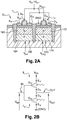
- FIG. 1A An example of a photosensitive logic cell structure, implemented according to the invention, is given on the figure 1A .
- This cell comprises a first transistor T 1 of a first type, for example of P type and a second transistor T 2 of a second type, for example of N type, which are juxtaposed and formed on a semi-type substrate.
- conductor on insulator for example of SOI type (SOI for “Silicon on Insulator” or silicon on insulator).
- the substrate comprises a semiconductor support layer 100, an insulating layer 101 resting on a face called the “front face” of the support layer 100, and a surface semiconductor layer 102 resting on the insulating layer 101 and in which the channel of the first transistor T 1 and of the second transistor T 2 are provided.
- the transistors T 1 and T 2 can be MOS transistors (MOS for “Metal Oxide Semiconductor”) produced for example according to a technology of SOI type completely deserted with thin buried oxide, called UTBB-FDSOI (for “Ultra-Thin Body”). and Box ”-“ Fully Depleted Silicon On Insulator ”).
- MOS Metal Oxide Semiconductor
- the surface semiconductor layer 102 has a thickness e 3 (measured in a direction parallel to a z axis of a mark [O; x; y; z]) which may be for example between 4 and 30 nm, preferably between 6 and 12 nm.
- the support layer 100 is configured so as to include a photosensitive zone 150 which extends opposite the first transistor T 1 and the second transistor T 2 , this photosensitive zone 150 being intended to receive light radiation R, which can penetrate for example in part through a rear face of the support layer 100 opposite to its front face.
- This photosensitive zone 150 comprises a first junction 160, for example a PN type junction facing the first transistor T 1 , and a second junction 170, for example a PN type junction facing the second transistor T 2 .
- the junctions 160, 170 can have a height also called thickness e 1 (measured parallel to the z axis of the reference mark [O; x; y; z]), for example between 100 nm and 5 ⁇ m.
- the first junction 160 and the second junction 170 each comprise a first doped zone 162, 172 according to a doping of a first type, for example of the N type, and a second zone 164, 174 doped according to a doping of a second type, for example of type P, the first zone and the second zone being superimposed.
- the arrangement of the doped zones 162, 164 forming the first junction 160 is such that the first N-doped zone 162 is arranged between the channel zone 104 of the first transistor T 1 and the second P-doped zone 164.
- the arrangement of the zones doped 172, 174 forming the second junction 170 is for its part such that the first N-doped zone 172 is disposed between the channel zone 124 of the second transistor T 2 and the second P-doped zone 174.
- the second P-doped zones 164, 174 are in this example lower zones of the junctions located on the side of the rear face of the support layer 100, while the first N-doped zones 162, 172 are upper zones of the junctions located on the side of the front face of the support layer 100.
- the photosensitive zone 150 can be arranged in the support layer 100 so as to be contiguous to the insulating layer 101 so that the upper doped zones 162, 172 of the junctions 160, 170 are in contact with the insulating layer 101.
- This insulating layer 101 is chosen sufficiently low so that a voltage photo-generated on the side of its rear face can induce a corresponding voltage by capacitive coupling on the side of its front face.
- the photosensitive zone 150 and the channel zone 104 of the first transistor T 1 are thus separated by means of the insulating layer 101, the configuration of which, in particular its composition and its thickness e 2 , are provided so as to allow establishing a capacitive coupling between the first junction 160 and the channel area 104 of the first transistor.
- the insulating layer 101 may for example be based on SiO 2 and have a thickness e 2 which may be for example between 5 nm and 50 nm, preferably between 10 and 25 nm.
- the capacitive coupling is such that a variation in potential subsequent to the reception of light radiation at the level of the photosensitive zone, and in particular of the first junction 160, can induce a variation LIVS P (with “LIVS” for “Light Induced V TP Shift ”or shift of the threshold voltage V TP induced by the light, this shift being denoted LIVS P for a transistor of type P) of the threshold voltage V TP of the first transistor T 1 .
- the photosensitive zone 150 and a channel zone 124 of the second transistor T 2 are separated by the intermediary of the insulating layer 101, configured such that a capacitive coupling between the photosensitive zone 150 and the channel zone is capable of being established and of making it possible to induce a variation denoted LIVS N of the threshold voltage V TN of the second transistor T 2 following the reception of a light radiation at the level of the photosensitive zone 150, and in particular of the second junction 160.
- the variation in threshold voltage V TP of the first transistor T 1 , and / or of that V TN of the second transistor T 2 , following an illumination or a variation in illumination of the photosensitive zone can for example reach a value of the order of 100 mV or even 350 mV or even 500 mV.
- the threshold voltage offset can be adjusted.
- a decrease in the thickness of the insulating layer 101, and / or an increase in the thickness e 3 of the surface semiconductor layer 102, and / or an increase in the thickness of the gate dielectric of the transistors are in particular favorable to an increase in this threshold voltage shift.
- An insulating trench 181 for example of the STI type (STI for "shallow trench insulation") is arranged between the first transistor T 1 and the second transistor T 2 and configured so as to provide electrical insulation between the first junction 160 and the second junction 170.
- This trench is filled with a dielectric material such as for example SiO 2 .
- the isolation can be such that when a photon is absorbed by the photosensitive zone 150 at one of the first junction 160 or second junction 170, the latter does not impact the other junction, that is to say say that it does not induce the creation of a charge carrier in this other junction.
- the trench 181 may have a height H 1 provided for example between 50 nm and 3 ⁇ m and may include an end 181a disposed in the support layer 100 and which protrudes with respect to the lower doped zone of the junctions 160, 170.
- a polarization of the first junction 160 completely independent of that of the second junction 170, ie with different polarization potentials can thus possibly be provided.
- One or more other insulating trenches 183, 185 can also be arranged around the first transistor T 1 and the second transistor T 2 .
- These other insulating trenches 183, 185 which can also be filled with dielectric material such as, for example, SiO 2 , are configured so as to provide electrical insulation between the logic cell and an external element also produced on the substrate, for example another. photosensitive logic cell or other element.
- the trenches 183, 185 arranged around the transistors T 1 , T 2 are arranged so that a photon absorbed at the photosensitive zone 150 of the logic cell does not impact another photosensitive zone of a logic cell neighbor (not shown).
- the trenches 183, 185 may have a height H 2 which may be provided greater than that H 1 of the insulating trench 181, and for example such that they protrude into the support layer 100 under the insulating layer 101 by a distance by example of the order of 200 nm.
- one or more conductive elements 191, 193, passing through the surface semiconductor layer 102, the insulating layer 101 and a part of the support layer 100 may be provided.
- a connection of the conductive elements 191, 193 to the lower doped areas 164, 174 can be established without making a connection with the upper doped areas 162, 172.
- the conductive elements 191, 193 can be in contact with regions of the doped areas 164, 174 which extend in a plane parallel to the main plane of the substrate (ie a plane parallel to the plane [O; x; y] on the figure 1 ) beyond the upper doped areas 162, 172 and beyond these areas.
- the first transistor T 1 and the second transistor T 2 also include source and drain zones which can be formed at least partially of semiconductor blocks 106, 108 arranged on the surface semiconductor layer 102.
- the first transistor T 1 and the second transistor T 2 also each include a gate block 110, the lateral flanks of which may be covered on either side with insulating zones forming first spacers 112.
- the first spacers 112 are partially buried in the respective active areas of transistors T 1 , T 2, while other insulating areas forming second spacers 114, rest on the respective active areas of transistors T 1 , T 2 and are placed against the first spacers 112.
- the respective gate blocks 110 of transistors T 1 , T 2 are placed on gate dielectric areas 109, for example based on SiO 2 and of the thick gate oxide type ("thick consultede oxide" or GO2) or of a “high-k” material such as HfO 2 .
- the gate dielectric zone 109 can have an inversion electrical thickness Tinv of for example between 0.7 nm and 7 nm, preferably between 1.5 nm and 4 nm.
- FIG. 1B An alternative embodiment of the cell of the figure 1A is given on the figure 1B
- the insulating trench 181 disposed between the junctions 160, 170 so as to achieve a separation between the doped zones 162, 172 is this time provided with a height H 1 such that the lower part of the insulating trench 181 is raised relative to the doped zones.
- 164, 174 lower of the junctions 160, 170, these lower doped zones being in contact with one another and being able this time to be put at the same polarization potential, preferably non-floating for example by means of a conductive element 191 to which a fixed voltage is applied. This can then make it possible to make the polarization of the junctions 160, 170 easier.
- FIG. 1C Another variant embodiment of the cell is given on figure 1C .
- the insulating trenches 183, 185 arranged around the junctions 160, 170 are this time provided with a height H 2 such that the lower part 183a, 185a of the trenches 183, 185 is raised relative to the lower doped zones 164, 174 of the junctions 160, 170, these lower doped zones being in contact with one of the other and being able this time to be polarized, by means of one or more conducting elements 197 arranged outside the photosensitive logic cell, around the latter. This can also make it possible to make the polarization of the junctions 160, 170 easier.
- the transistors T 1 , T 2 on a substrate of SGOI type (for “SiGe-on-insulator”), that is to say of which the surface semiconductor layer 102 is based on SiGe, or else on a substrate of the semiconductor on insulator type, the surface layer 102 of which is based on a III-V semiconductor material.
- SiGe-on-insulator for “SiGe-on-insulator”
- the junctions 160, 170 can be formed in the support layer of the substrate 100 of the semiconductor type by ion implantation through the stack formed of the semiconductor layer. surface conductor 102 and the insulating layer 101 of BOX.
- the implantation steps are preferably followed by at least one annealing step to repair the defects created by the implantation.
- the annealing can be carried out, for example, between 550 ° C. and 1200 ° C., with a duration chosen from a range between one msec and ten minutes.
- the implantation annealing can be carried out at 1050 ° C. for 5 s.
- junctions 160, 170 comprises a step of transferring them to the rear face of the insulating layer 102 of BOX, for example by gluing.
- junctions can also be produced by epitaxy of a semiconductor material such as, for example, Si, or SiGe, or Ge, or InGaAs, or InP, or GaN, or InGaN on the support layer 100, for example by performing in-situ doping or else doping by species diffusion.
- a semiconductor material such as, for example, Si, or SiGe, or Ge, or InGaAs, or InP, or GaN, or InGaN on the support layer 100, for example by performing in-situ doping or else doping by species diffusion.
- the photosensitive logic cell of figures 1A-1C can be configured so as to form a photosensitive logic inverter, in particular of the CMOS type.
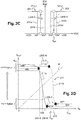
- FIG. 2A-2B A first example of configuration of a CMOS photosensitive logic inverter formed from the cell of the figure 1 , is given on figures 2A-2B , while the figures 2C-2D serve to illustrate the operation of this inverter.
- the logic state of a signal V OUT emitted at the output of the inverter depends on the quantity of photons received by the photosensitive zone opposite the first transistor T 1 and the second transistor T 2 .
- the logic inverter comprises a terminal IN connected to the respective gates G P and G N of the first transistor T 1 and of the second transistor T 2 , the gates G P and G N being connected to each other.
- An output OUT of the inverter making it possible to deliver the logic or binary signal V OUT , is connected to the respective drains D P and D N of the first transistor T 1 and of the second transistor T 2 , the drains D P and D N being connected between them ( figure 2B ).
- the device also comprises a means for biasing the source of the first transistor T 1 provided to apply a potential V DD to the source S P, for example of the order of 1V for transistors having a gate length of between 30 and 35 nm , or 0.9V for transistors having a gate length between 26 nm and 32 nm, or 0.75V for transistors having a gate length between 18 nm and 24 nm.
- a means for biasing the source of the first transistor T 1 provided to apply a potential V DD to the source S P, for example of the order of 1V for transistors having a gate length of between 30 and 35 nm , or 0.9V for transistors having a gate length between 26 nm and 32 nm, or 0.75V for transistors having a gate length between 18 nm and 24 nm.
- the source S N of the second transistor T 2 can be placed at a reference potential V SS or GND serving as ground.
- the transistors T 1 and T 2 are in this example biased so as to have a constant gate-source voltage V GS , the change of conduction state on or off of the transistors being obtained by shifting their threshold voltages V TN , V TP respective due to a variation in illumination of the photosensitive zone.
- Means for polarizing respectively the first junction 160 and the second junction 170 are also provided. These biasing means are configured to apply a first potential Vpoll, for example of the order of -5V to 5V to the lower doped zone 162 (in this example N-doped) of the first junction 160 and to apply a second potential Vpol2, for example of the order of -5V to 5V at the lower doped zone 172 (in this N doped example) of the second junction 170 while the respective upper doped zones of the junctions 160, 170 (in this example the zones 164, 174 doped P) are set to a floating potential.
- Vpoll for example of the order of -5V to 5V
- Vpol2 for example of the order of -5V to 5V
- Vpol2 for example of the order of -5V to 5V at the lower doped zone 172 (in this N doped example) of the second junction 170 while the respective upper doped zones of the junctions 160, 170 (in this example the zones 164, 174 do
- the amplitude of the threshold voltage shift induced by the LIVS light depends for each transistor on a ratio called “Body Factor”. »Capacitance between its channel and a region of the photosensitive zone playing the role of a back gate,
- the Body Factor depends on the bias potential applied (respectively Vpol1 for the first transistor and Vpol2 for the second transistor) to the zones spiked lower 172, 174.
- Provision can for example be made to apply the same bias potential Vpol1 Vpol2 to the lower doped zone 162 and to the lower doped zone 172.
- Vpol 1 and Vpol 2 can be applied respectively to the lower doped zone 162 and to the lower doped zone 172, so as to implement a threshold voltage shift induced by the light LIVS P for the first P-type transistor different from the LIVS N light-induced threshold voltage offset for the second N-type transistor.
- Vpoll, Vpol2 applied to control the threshold voltage shift LIVS depends on the direction of the junction (P / N or N / P), under the insulating layer of BOX on which the channels of the transistors rest.
- curves 201, 202 of respective variations of the drain-source currents of the first transistor T 1 and of the second transistor T 2 as a function of their respective gate-source voltages are given.
- This figure shows shifts in threshold voltages LIVS P of the first transistor T 1 and LIVS N of the second transistor T 2 generated by the reception of a given quantity of photons or by a given increase in a quantity of photons received by the zone photosensitive arranged opposite the transistors T 1 , T 2 .
- the threshold voltage of the first transistor T 1 is liable to change from a value Vtp when the photosensitive zone is not illuminated or insufficiently illuminated (portion 201a of the curve 201 in continuous line) to a value Vtp * when the photosensitive zone is illuminated or sufficiently illuminated (portion 201b of curve 201 in broken line), with
- can be increased by decreasing the thickness e 2 of the insulating layer 101 of the weaker substrate, and / or by increasing the chosen thickness e 3 of the surface semiconductor layer, and / or by increasing the chosen thickness of the dielectric gate of the first transistor T 1 .
- the threshold voltage of the second transistor T 2 is liable to change from a value Vtn when the photosensitive zone is not illuminated or is insufficiently illuminated (portion 202a of the curve 202 in solid lines) to a value Vtn * when the photosensitive zone is illuminated or sufficiently illuminated (portion 202b of the curve 202 in broken lines), with Vtn * -Vtn which can be for example of the order of 100 mV.
- the arrangement of the P and N doped zones of the junctions 160, 170 is such that a change in illumination of the photosensitive zone causes a shift of the respective threshold voltages Vtn and Vtp of the transistors in the same one. direction of variation (VtN increasing and VtP decreasing in absolute value).
- VtN increasing and VtP decreasing in absolute value
- an increase in the quantity of photons received by the photosensitive zone of the logic inverter is here likely to induce a decrease (in absolute value) in the threshold voltage of the first transistor T 1 (of type P) and an increase of the threshold voltage of the second transistor T 2 (of type N).
- the 2D figure illustrates a transfer function of the output signal V OUT as a function of the signal applied to the input of the first example of a logic inverter when the latter is subjected to light radiation (portion of curve 211a) and when the latter is not subjected to light radiation (portion of curve 211b).
- the bias potential V NP is in this example chosen so as to be greater than a potential V M corresponding to the potential for which the potential V OUT at the output OUT of the inverter is equal to the potential V IN applied to the terminal IN.
- the bias potential V NP is preferably chosen such that V NP is greater than V M + ⁇ with ⁇ a voltage dependent on the noise margin and which is a function of the voltage V DD .
- V IN V NP applied to the terminal IN is advantageously chosen such that: V M + ⁇ ⁇ V NP ⁇ V M + ⁇ + LIVS NOT + LIVS P 2
- the bias potential V NP of the input IN can be chosen for example so that V NP ⁇ [VM; VM + 200 mV] V M depending on Vt N , Vtp, and on V DD .
- the first example of a photonic logic inverter can thus follow the following truth table: IN Light OUT V NP NO 0 V NP YES 1
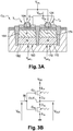
- FIG. 3A-3B A second example of a photosensitive logic inverter configuration is given on the figures 3A-3B , while the figures 3C-3D serve to illustrate how it works.
- the configuration of the second example of an inverter differs from that of the inverter described above in particular by the arrangement of the junctions 160, 170.
- the arrangement of the doped zones 162, 164 forming the first junction 160 is in this example ( figure 3A ) such that the P-doped zone 164 is arranged between the channel zone 104 of the first transistor T 1 and the N-doped zone 162.
- the arrangement of the doped zones 172, 174 forming the second junction 170 is itself such that the zone 174 P doped is disposed between the channel zone 124 of the second transistor T 2 and the second N doped zone 172.
- the second P-doped zones 164, 174 form in this example the upper zones of the junctions, while the N-doped zones 162, 172 form the lower zones of the junctions.
- Polarization means respectively of the first junction 160 and of the second junction 170 may be provided to apply a first potential Vpol 1 to the lower doped zone 162 (in this example doped N) of the first junction 160 and a second potential Vpol 2 to the lower doped zone 172 (in this example doped N) of the second junction 170, while the respective upper doped zones of the junctions 160, 170 in this example the P-doped zones 164, 174 of the junctions are set to a floating potential.
- the configuration of the second example of an inverter is similar to that of the first example of an inverter described above.
- the transistors T 1 and T 2 are thus biased so as to have a constant gate-source voltage V GS , a respective change of on or off state of the transistors being able to be obtained by varying their respective threshold voltages V TP and V TN. , this variation being itself dependent on the state of illumination of the photosensitive zone.
- the figure 3C gives variation curves 301, 302 of the respective drain-source currents of the first transistor T 1 and of the second transistor T 2 as a function of their respective gate-source voltages. It shows LIVS P and LIVS N offsets (illustrated respectively by an offset between the curve portion 301a and the curve portion 301b for the P-type transistor and by an offset between the curve portion 302a and the curve portion 302b for the N-type transistor) of the respective threshold voltages of the first transistor and of the second transistor generated by an illumination or an increase in illumination of the photosensitive zone.
- the threshold voltage of the first transistor T 1 (of type P) increases in absolute value, while the threshold voltage of the second transistor T 2 (of type N) decreases in absolute value.
- the threshold voltage shift Vt is done here in the same direction (negative).
- the input IN of the inverter is biased to a potential V Fixed PN chosen from a range (portion 310 on the abscissa axis of the 3d figure ) of suitable voltages.
- the bias potential V PN is in this example chosen so as to be less than the potential V M and preferably such that V PN is less than V M - ⁇ with ⁇ a voltage dependent on the noise margin.
- V PN applied to the terminal IN is advantageously chosen such that: For a BOX / P / N arrangement of the doped zones of the junctions as illustrated on the figure 3A , we define V PN by: V M - ⁇ - LIVS P + LIVS NOT 2 ⁇ V PN ⁇ V M - ⁇ with LIVS P > 0 and LIVSN ⁇ 0.
- the second example of a photonic logic inverter can thus follow the following truth table: IN Light OUT V NP NO 1 V NP YES 0
- photosensitive cells as described above, it is possible to implement a logic circuit capable of being controlled by light and whose functions, in particular logic, can be modified as a function of the level of illumination that this logic circuit receives.
- the 2D figures and 3d show that, in a certain voltage range applied to the input IN of a photosensitive logic inverter, it is possible to switch, by a variation in illumination and a sufficient supply of photons, the logic output OUT of the inverter, the logic state of this output OUT not switching when the supply of photons is insufficient.
- the function which can be modified by lighting can be, for example, a function of collective programming of cells or of reset.
- Such a logic circuit can be implemented, for example, so that a brief light pulse or a light flash makes it possible to switch a set of photosensitive logic inverters.
- a logic circuit controlled, or programmed, or reset, without requiring specific addressing, by means of a light flash applied for example to the rear face of a chip on which this circuit is mounted can thus be produced.
- a photosensitive logic inverter configuration variant is given on the figures 4A-4B , the figures 4C-4E used to illustrate its operation.
- the logic state '1' or '0' of the output signal V OUT of the inverter does not depend here, unlike the examples previously described, on the quantity of photons received by the photosensitive zone in other words on the 'illumination state of the latter, but of a logic state' 0 'or' 1 'of an electrical input signal V IN applied to input IN of the inverter.
- this photosensitive logic inverter configuration variant differs from the examples described above by the type of signal V IN applied to input IN ( figure 4B ), this signal being a variable voltage, capable of adopting at least a first value for which the transistor T 1 of type P is off while the transistor T 2 of type N is on, and at least a second value for which the transistor T 1 of type P is on while the transistor T 2 of type N is blocked.
- This third example of an inverter also differs from those described above by the arrangement of the junctions 160, 170.
- the arrangement of the doped areas 162, 164 forming the first junction 160 is such that the P-doped area 164 is disposed on the N-doped area 162, while that of the second junction 170 is such that the N-doped area 172 is disposed on P-doped zone 174 ( figure 4A ).
- curves 401, 402 of respective variations of the drain-source currents of the first transistor T 1 and of the second transistor T 2 as a function of their respective gate-source voltages are given.
- an increase in the quantity of photons received by the photosensitive zone is capable of generating an increase in the threshold voltage of the second transistor T 2, this increase being reflected by a shift between a portion of curve 402a in solid line illustrating a non-illuminated state of the photosensitive area and a portion of curve 402b in broken lines illustrating an illuminated state of the photosensitive area.
- an increase in the quantity of photons received by the photosensitive zone is capable of generating an increase (in absolute value) in the threshold voltage of the first transistor T 1 .
- the photosensitive logic inverter has a transfer function of a conventional inverter when it does not receive light radiation.
- the speed of transition at output OUT from one logic state to another logic state then results in a given slope of the portion of curve 411 on the figure 4D .
- the speed of transition from one logic state to another logic state is in this case greater, which results in a slope of the portion of curve 412 on the figure 4D higher than that of the curve portion 411.
- FIGS. 5A-5D serve to illustrate another example of a photosensitive logic inverter configuration which differs from the example previously described in particular by the arrangement of the junctions 160, 170 ( figure 5A ).
- the arrangement of the doped zones 162, 164 forming the first junction 160 is such that the N-doped zone 162 is disposed between the channel zone 104 of the first transistor T 1 and the P-doped zone 164.
- doped areas 172, 174 forming the second junction 170 is for its part such that the P-doped area 174 is disposed between the channel area 124 of the second transistor T 2 and the N-doped area 172.
- the figure 5C gives curves 501, 502 of respective variations of the drain-source currents of the first transistor T 1 and of the second transistor T 2 as a function of their gate-source voltages and shows that an increase in the quantity of photons received by the photosensitive zone is capable of generating a decrease (in absolute value) in the threshold voltage of the first transistor T 1 (decrease reflected by a shift between a portion of curve 501a in solid line illustrating a non-illuminated state of the photosensitive zone and a portion of curve 501b in dashed line illustrating an illuminated state of the photosensitive zone) while a decrease in the threshold voltage of the second transistor T 2 (decrease reflected by a shift between a portion of curve 501a in solid line illustrating a non-illuminated state of the photosensitive zone and a portion of curve 502b in broken lines illustrating an illuminated state of the photosensitive zone).
- the switching speed from one logic state to another logic state at output OUT depends on the illumination state of the photosensitive zone ( figure 5D ).
- a photosensitive logic inverter matrix arrangement according to one or the other of the embodiments described above can be provided.
- a photosensitive logic inverter according to one or other of the configurations described above, it is also possible to implement a logic circuit comprising at least one logic gate requiring a logic function. inverting or "NOT”, for example a logic gate “NAND” ( figure 6A ) photosensitive or “NO OR” photosensitive ( figure 6B ).
- NOT for example a logic gate “NAND” ( figure 6A ) photosensitive or “NO OR” photosensitive
- a photosensitive logic inverter can also be integrated in a circuit forming a photosensitive latch ( figure 6C ), for example an SRAM memory switch.
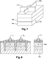
- the figure 8 illustrates an exemplary embodiment of the first P-type transistor T 1 of the photosensitive logic cell according to such finFET technology.
- the junction 160 formed of the superimposed N-doped zone 162 and of the P-doped zone 164 extends in the support layer facing a portion of the semiconductor bar 704 covered by the gate 710 and intended to form a channel.
- a photosensitive logic inverter as described above can be integrated within a device comprising one or more other transistors, for example transistors of a processing circuit, the threshold voltage of which does not vary or varies little as a function of light radiation received by an area of the support layer located opposite the latter.
- FIG 8 an example of such a device is illustrated and comprises a transistor T 3 juxtaposed with transistors T 1 and T 2 forming a photosensitive logic cell opposite which a single doped zone 895 is provided in a region of the support layer 100.
- This doped zone 895 for example of type P and to which a polarization potential can be applied, forms a ground plane ("ground plane" according to the English terminology) replacing the photosensitive zone, in order to make the transistor T 3 insensitive to light radiation.
- a photosensitive logic inverter according to the invention can be integrated into a device comprising several levels of superimposed transistors.
- FIG 9 an example of such a device is illustrated and comprises a transistor T 3, for example of a processing circuit located at a given level N k of a plurality of levels of superimposed components, while the transistors forming the logic inverter photosensitive (only the P-type transistor T 1 being illustrated in this figure) are located at a higher level N k + 1 .
- transistor T 3 may be insensitive to light radiation, so that its threshold voltage does not vary or varies little as a function of the quantity of photons received by the device.
- the channel zone of transistor T 3 is not located opposite a junction capable of acting on its threshold voltage.
- the creation of defects by implantation in the junctions may possibly make it possible to facilitate this discharge.
- Another way to allow rapid discharge of the BOX / junction interface without modifying the structure of the cells is to provide a cell (s) polarization control circuit configured to emit a specific initialization pulse or erasure.
- This pulse is in the form of a voltage step or an edge whose direction of variation depends on the type of PN or NP junction located under the insulating layer of BOX.
- This initialization or erasure pulse can be applied to the respective gates of the transistors of the cell located opposite the junctions and transmitted by electrostatic or capacitive coupling.
- the initialization or erasure pulse can be emitted periodically during an initialization or erasure phase scheduled during each cycle of the photosensitive logic cell and can precede or follow each reading phase in which the logic state of the cell is read.
- an example of the operating sequence of a matrix of photosensitive logic cells comprises an initialization phase of the matrix, then a waiting phase, for example of the order of several nanoseconds during which the cells illuminated are loaded, then a reading phase. Then, such a sequence is repeated.
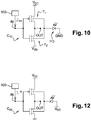
- the figure 10 illustrates an example of a device provided with such a polarization control circuit 100 adapted to a photosensitive logic cell C 10 .
- This C 10 cell has a junction configuration similar to that of the cell previously described in connection with the figures 3A and 3B , that is to say with P-doped areas arranged on the N-doped areas and thus interposed between the N-doped areas and the BOX insulating layer.
- the representation used to show the coupling effect between the front face and the rear face of the substrate is such that the transistors are shown with a second gate on the rear face, the junctions being symbolized by a PD photodiode.
- the voltage step emitted by circuit 100 to allow the discharge at the BOX / junction interface to be accelerated is a voltage step positive, applied to the IN terminal connected to the gates of transistors T 1 and T 2 of cell C 20 .
- the amplitude of the step depends in particular on the type of transistors and on the technology in which the transistors of the cell are made.
- the respective sources of transistors T 1 , T 2 can advantageously be placed by the bias control circuit 100 at a ground potential GND in order to minimize the leaks.
- the bias control circuit 100 applies an ascending voltage step to the gate of transistors T 1 and T 2 of cell C 10 .
- a step can also be applied to the source and drain regions of transistors T 1 , T 2 .
- Such a step can also be applied to a gate of transistors T 1 , T 2 placed on the rear face and interposed between the junction and the insulating layer of BOX.
- the figures 11A-11B illustrate the effect of a voltage step ( figure 11B ) on the strip structure on the rear face of cell C 20 .
- the figure 12 illustrates an alternative embodiment suitable for a photosensitive logic cell C 20 , the configuration of which is similar to that described above in connection with the figures 2A and 2B , that is to say in which the N-doped areas of the junctions are arranged on the P-doped areas and are thus interposed between the P-doped areas and the BOX insulating layer.
- the voltage step emitted by circuit 100 to make it possible to accelerate the discharge at the BOX / junction interface is a voltage step descending, applied to the terminal IN connected to the respective gates of the first transistor T 1 and of the second transistor T 2 .
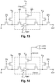
- a polarization control circuit using NMOS and PMOS transistors and configured to modify the polarization state of a photosensitive logic cell C 10 as described previously in connection with the figure 10 are given on figures 13 and 14 .
- the state of polarization of the photosensitive logic cell C 10 depends on the logic state of read signals RD and erase ER.
Description
La présente invention se rapporte au domaine des dispositifs photosensibles et concerne la mise en œuvre d'une cellule logique photosensible encore appelée inverseur logique photonique.The present invention relates to the field of photosensitive devices and relates to the implementation of a photosensitive logic cell also called a photonic logic inverter.
Dans le domaine technique des dispositifs photosensibles, le document
A l'aide d'un tel dispositif, on peut chercher à mettre en œuvre un mode de détection binaire de rayonnement lumineux.Using such a device, one can seek to implement a binary light radiation detection mode.
Il se pose le problème de réaliser un nouveau dispositif photosensible susceptible de réaliser une détection de rayonnement lumineux, et de pouvoir traduire cette détection sous forme d'un signal numérique, le tout en ayant un encombrement limité.The problem arises of producing a new photosensitive device capable of carrying out a detection of light radiation, and of being able to translate this detection into the form of a digital signal, while having a limited size.
La présente invention concerne tout d'abord une cellule logique photosensible selon la revendication 1.The present invention relates firstly to a photosensitive logic cell according to
Le premier transistor et le deuxième transistor sont agencés selon une configuration d'inverseur logique CMOS.The first transistor and the second transistor are arranged in a CMOS logic inverter configuration.
Ainsi, le premier transistor peut être doté d'une grille connectée à celle du deuxième transistor, tandis que le drain du premier transistor est connecté au drain du deuxième transistor.Thus, the first transistor can be provided with a gate connected to that of the second transistor, while the drain of the first transistor is connected to the drain of the second transistor.
Selon une première possibilité de mise en œuvre de la cellule logique photosensible, le signal d'entrée faisant varier l'état de la sortie de la cellule logique est un signal lumineux.According to a first possibility of implementing the photosensitive logic cell, the input signal varying the state of the output of the logic cell is a light signal.
Selon la première possibilité de mise en œuvre de la cellule logique photosensible, celle-ci peut être configurée de manière à délivrer en sortie un signal logique VOUT ayant un premier état logique lorsque la zone photosensible est soumise à un premier éclairement, par exemple un éclairement nul ou faible, et pour délivrer en sortie un signal logique VOUT ayant un deuxième état logique, lorsque la zone photosensible est soumise à un deuxième éclairement, plus important que le premier éclairement.According to the first possibility of implementing the photosensitive logic cell, the latter can be configured so as to output a logic signal V OUT having a first logic state when the photosensitive zone is subjected to a first illumination, for example a zero or low illumination, and to deliver at output a logic signal V OUT having a second logic state, when the photosensitive zone is subjected to a second illumination, greater than the first illumination.
Selon cette première possibilité de mise en œuvre, la première jonction et la deuxième jonction peuvent être dotées chacune d'une zone inférieure dopée P surmontée d'une zone supérieure dopée N.According to this first possibility of implementation, the first junction and the second junction can each be provided with a lower P-doped zone surmounted by an upper N-doped zone.
En variante, la première jonction et la deuxième jonction comprennent chacune une zone dopée N surmontée d'une zone supérieure dopée P.As a variant, the first junction and the second junction each comprise an N-doped zone surmounted by an upper P-doped zone.
Selon la première possibilité de mise en œuvre de la cellule, celle-ci peut comprendre également une entrée mise à un potentiel de polarisation fixe VNP ou VPN prédéterminé qui est appliqué aux grilles du premier et du deuxième transistor, le premier transistor et le deuxième transistor étant polarisés de manière à avoir des tensions grille-source respectives constantes.According to the first possibility of implementing the cell, the latter may also comprise an input set to a predetermined fixed bias potential V NP or V PN which is applied to the gates of the first and of the second transistor, the first transistor and the second transistor being biased so as to have constant respective gate-source voltages.
On peut ainsi avantageusement réaliser une cellule logique photosensible dont l'état logique de sa sortie dépend uniquement de la quantité de photons reçus.It is thus advantageously possible to produce a photosensitive logic cell whose logic state of its output depends solely on the quantity of photons received.
La première jonction peut avantageusement être polarisée indépendamment de la deuxième jonction.The first junction can advantageously be polarized independently of the second junction.
On peut ainsi prévoir des moyens pour appliquer un premier potentiel de polarisation sur la première jonction et des moyens pour appliquer un deuxième potentiel de polarisation différent du premier potentiel sur la deuxième jonction. Dans ce cas, pour un même changement d'état d'éclairement entre la première jonction et la deuxième jonction, on peut avantageusement mettre en œuvre une modulation de tension de seuil du premier transistor différente de celle mise en œuvre pour le deuxième transistor.Means can thus be provided for applying a first polarization potential to the first junction and means for applying a second polarization potential different from the first potential to the second junction. In this case, for the same change of illumination state between the first junction and the second junction, it is advantageously possible to implement a threshold voltage modulation of the first transistor different from that implemented for the second transistor.
Afin de réaliser une isolation électrique entre la première jonction et la deuxième jonction, la cellule peut comprendre en outre au moins une tranchée isolante entre le premier transistor et le deuxième transistor, la tranchée isolante traversant la couche de support.In order to achieve electrical insulation between the first junction and the second junction, the cell may further comprise at least one insulating trench between the first transistor and the second transistor, the insulating trench passing through the support layer.
Des moyens de polarisation peuvent être prévus et configurés pour appliquer un potentiel Vpol déterminé de polarisation à la zone inférieure de la première jonction et/ou de la deuxième jonction, la zone supérieure de la première jonction et/ou de la deuxième jonction étant alors mise à un potentiel flottant.Biasing means can be provided and configured to apply a determined bias potential Vpol to the lower zone of the first junction and / or of the second junction, the upper zone of the first junction and / or of the second junction then being placed. at a floating potential.
Selon une deuxième possibilité de mise en œuvre de la cellule logique photosensible, le signal d'entrée faisant varier l'état de sortie de la cellule logique est un signal logique de nature électrique.According to a second possibility of implementing the photosensitive logic cell, the input signal causing the output state of the logic cell to vary is a logic signal of an electrical nature.
Pour cette variante de mise en œuvre, la vitesse de commutation d'un état logique à un autre en sortie de la cellule dépend de l'état d'éclairement de la cellule.For this variant of implementation, the switching speed from one logic state to another at the output of the cell depends on the lighting state of the cell.
Une deuxième possibilité de mise en œuvre de la cellule logique photosensible, prévoit ainsi un moyen pour appliquer un potentiel variable VIN en entrée de l'inverseur.A second possibility of implementing the photosensitive logic cell thus provides a means for applying a variable potential V IN at the input of the inverter.
Dans ce cas, on peut ainsi avantageusement réaliser un inverseur logique photosensible dont l'état logique de sa sortie dépend du potentiel VIN en entrée, comme pour un inverseur logique classique, mais dont la vitesse de transition de sa sortie entre deux états logiques dépend de la quantité de photons reçus par cette dernière, et en particulier de si la zone photosensible est exposée ou non à un rayonnement lumineux.In this case, it is thus advantageously possible to produce a photosensitive logic inverter whose logic state of its output depends on the potential V IN at the input, as for a conventional logic inverter, but on which the speed of transition of its output between two logic states depends. of the quantity of photons received by the latter, and in particular of whether or not the photosensitive zone is exposed to light radiation.
Selon cette deuxième possibilité de mise en œuvre de la cellule logique photosensible, l'agencement des jonctions peut être tel que la première jonction comprend une zone inférieure dopée N surmontée d'une zone supérieure dopée P, la deuxième jonction comprenant une zone inférieure dopée P surmontée d'une zone supérieure dopée N. En variante, la première jonction comprend une zone inférieure dopée P surmontée d'une zone supérieure dopée N, la deuxième jonction comprenant une zone inférieure dopée N surmontée d'une zone supérieure dopée P. La première jonction et la deuxième jonction sont ainsi orientées dans des sens différents.According to this second possibility of implementing the photosensitive logic cell, the arrangement of the junctions may be such that the first junction comprises an N-doped lower zone surmounted by a P-doped upper zone, the second junction comprising a P-doped lower zone surmounted by an upper N-doped zone. As a variant, the first junction comprises a lower P-doped zone surmounted by an upper N-doped zone, the second junction comprising a lower N-doped zone surmounted by an upper P-doped zone. junction and the second junction are thus oriented in different directions.
Selon une possibilité de mise en œuvre de la cellule logique photosensible, on peut prévoir une zone isolante autour du premier transistor et/ou du deuxième transistor. Cette zone isolante peut traverser la couche de support et être configurée de manière à isoler électriquement ladite cellule, en particulier sa zone photosensible, par rapport à une autre cellule ou un autre élément formé dans le substrat.According to one possible implementation of the photosensitive logic cell, an insulating zone can be provided around the first transistor and / or the second transistor. This insulating zone can pass through the support layer and be configured so as to electrically isolate said cell, in particular its photosensitive zone, with respect to another cell or another element formed in the substrate.
La cellule logique photosensible peut être intégrée à un dispositif comprenant un ou plusieurs autres transistors dont la tension de seuil ne varie pas ou varie peu en fonction de l'éclairement du dispositif. Ces autres transistors peuvent être par exemple des transistors d'un circuit de traitement de signal connecté à la cellule logique photosensible.The photosensitive logic cell can be integrated into a device comprising one or more other transistors whose threshold voltage does not vary or varies little as a function of the illumination of the device. These other transistors can for example be transistors of a signal processing circuit connected to the photosensitive logic cell.
Selon une possibilité de mise en œuvre, ces autres transistors peuvent être formés en regard d'un plan de masse réalisé dans la couche de support semi-conductrice.According to one possible implementation, these other transistors can be formed facing a ground plane produced in the semiconductor support layer.
Selon une possibilité de mise en œuvre, la cellule logique photosensible peut être intégrée à un dispositif dont les composants sont répartis sur plusieurs niveaux et comprenant en outre au moins un autre transistor agencé de sorte que la cellule logique et cet autre transistor sont superposés.According to one possible implementation, the photosensitive logic cell can be integrated into a device whose components are distributed over several levels and further comprising at least one other transistor arranged so that the logic cell and this other transistor are superimposed.
Selon une possibilité de mise en œuvre de la cellule logique photosensible, les transistors peuvent être réalisés selon une technologie de type FDSOI ou UTBB-FDSOI.According to a possible implementation of the photosensitive logic cell, the transistors can be produced according to a technology of the FDSOI or UTBB-FDSOI type.
La présente invention concerne également un circuit logique pour réaliser une fonction logique déterminée telle qu'une fonction NON ET ou NON OU, ce circuit comprenant une cellule logique photosensible telle que définie plus haut.The present invention also relates to a logic circuit for performing a determined logic function such as a NAND or NOT OR function, this circuit comprising a photosensitive logic cell as defined above.
La présente invention concerne également une cellule de mémoire SRAM (pour « Static Random Access Memory ») dont la bascule est formée d'une cellule logique photosensible telle que définie plus haut.The present invention also relates to an SRAM (for “Static Random Access Memory”) memory cell, the latch of which is formed by a photosensitive logic cell as defined above.
La présente invention concerne également un circuit logique photosensible comprenant une pluralité de cellules telles que définies plus haut.The present invention also relates to a photosensitive logic circuit comprising a plurality of cells as defined above.
La présente invention concerne également un circuit logique photosensible réalisant une fonction logique donnée et doté d'une ou plusieurs cellules logiques photosensibles telles que définie(s) plus haut, la fonction logique, telle qu'une fonction de programmation collective ou de remise à zéro, étant modifiable en fonction de l'éclairement du dispositif.The present invention also relates to a photosensitive logic circuit performing a given logic function and provided with one or more photosensitive logic cells as defined above, the logic function, such as a collective programming or reset function. , being modifiable according to the lighting of the device.
Selon un mode de réalisation, la présente invention prévoit un dispositif comprenant :
- une ou plusieurs cellules telles que définies plus haut et munies de jonctions formées chacune d'une zone dopée N surmontée d'une zone supérieure dopée P ou d'une zone dopée P surmontée d'une zone supérieure dopée N et
- un circuit de commande de polarisation configuré pour appliquer un échelon de tension au premier transistor et au deuxième transistor et placer la cellule dans un état d'effacement ou de réinitialisation.
- one or more cells as defined above and provided with junctions each formed by an N-doped zone surmounted by a P-doped upper zone or by a P-doped zone surmounted by an N-doped upper zone and
- a bias control circuit configured to apply a voltage step to the first transistor and the second transistor and place the cell in an erase or reset state.
Un tel échelon de tension peut permettre de décharger des régions situées à l'interface entre la couche isolante du substrat et respectivement la première et la deuxième jonction.Such a voltage step can make it possible to discharge regions located at the interface between the insulating layer of the substrate and respectively the first and the second junction.
La présente invention sera mieux comprise à la lecture de la description d'exemples de réalisation donnés, à titre purement indicatif et nullement limitatif, en faisant référence aux dessins annexés sur lesquels :
- les
figures 1A-1C illustrent un exemple de structure de cellule logique photo-sensible mise en œuvre suivant l'invention et comportant un premier transistor et un deuxième transistor de type différents disposés en regard d'une zone photosensible, cette zone comprenant une première jonction et une deuxième jonction couplées par couplage capacitif respectivement au canal du premier transistor et au canal du deuxième transistor; - les
figures 2A-2B illustrent un premier exemple de configuration de d'inverseur logique photosensible formé à partir de la cellule de lafigure 1 , pour laquelle l'état logique de la sortie de l'inverseur dépend d'une quantité de photons reçue par celui-ci, tandis que lesfigures 2C-2D illustrent des caractéristiques électriques de fonctionnement de cet inverseur ; - les
figures 3A-3B illustrent un deuxième exemple de configuration de d'inverseur logique photosensible suivant l'invention pour laquelle l'état logique de la sortie de l'inverseur dépend également du niveau d'éclairement de celui-ci, tandis que lesfigures 3C-3D illustrent des caractéristiques électriques de fonctionnement de cet inverseur; - les
figures 4A-4B illustrent un troisième exemple de configuration d'inverseur logique photosensible suivant l'invention pour laquelle l'état logique de la sortie de l'inverseur dépend de celui de son entrée, et pour laquelle la vitesse de commutation d'un état logique à un autre en sortie de l'inverseur dépend du niveau d'éclairement de celui-ci, tandis que lesfigures 4C-4E illustrent des caractéristiques électriques de fonctionnement de cet inverseur ; - les
figures 5A-5B illustrent un quatrième exemple de configuration d'inverseur logique photosensible suivant l'invention, tandis que lesfigures 5C-5D illustrent des caractéristiques électriques de fonctionnement de cet inverseur ; - les
figures 6A, 6B, 6C illustrent des exemples de fonctions logiques susceptibles d'être mises en œuvre à l'aide d'un inverseur logique photosensible suivant l'invention ; - la
figure 7 illustre un exemple de transistor réalisé en technologie finFET pour la mise en œuvre d'un inverseur logique photosensible suivant l'invention ; - la
figure 8 illustre un exemple de réalisation dans lequel les transistors d'une cellule logique photosensible sont juxtaposés à un transistor dont la tension de seuil ne varie pas ou varie peu en fonction d'une quantité de photons reçue ; - la
figure 9 illustre un exemple de dispositif à composant superposés sur plusieurs niveaux doté d'une cellule logique photosensible suivant l'invention ; - La
figure 10 illustre un exemple de moyen pour permettre de décharger une accumulation d'électrons à l'interface entre la couche isolante de BOX et les jonctions PN d'une cellule du type de celle de lafigure 3A ; - Les
figures 11A-11B illustrent l'effet d'un échelon de tension appliqué sur la cellule logique de lafigure 10 pour permettre de décharger une accumulation d'électrons à l'interface entre la couche isolante de BOX ; - La
figure 12 illustre un exemple de moyen pour permettre de décharger une accumulation de trous à l'interface entre la couche de BOX et les jonctions NP d'une cellule du type de celle de lafigure 2A ; - Les
figures 13 et 14 illustrent différents exemples de réalisation d'un circuit de commande de polarisation adapté pour mettre des cellules logiques photosensibles dans différents états de polarisation et en particulier pour réaliser un effacement lors duquel une décharge de porteurs accumulés à l'interface entre la couche isolante de BOX et les jonctions est mise en œuvre;
- the
figures 1A-1C illustrate an example of a photosensitive logic cell structure implemented according to the invention and comprising a first transistor and a second transistor of different types arranged facing a photosensitive zone, this zone comprising a first junction and a second coupled junction by capacitive coupling respectively to the channel of the first transistor and to the channel of the second transistor; - the
figures 2A-2B illustrate a first example of configuration of a photosensitive logic inverter formed from the cell of thefigure 1 , for which the logic state of the output of the inverter depends on a quantity of photons received by it, while thefigures 2C-2D illustrate the electrical operating characteristics of this inverter; - the
figures 3A-3B illustrate a second example of configuration of a photosensitive logic inverter according to the invention for which the logic state of the output of the inverter also depends on the level of illumination of the latter, while thefigures 3C-3D illustrate the electrical operating characteristics of this inverter; - the
figures 4A-4B illustrate a third example of a photosensitive logic inverter configuration according to the invention for which the logic state of the output of the inverter depends on that of its input, and for which the speed of switching from one logic state to another at the output of the inverter depends on the level of illumination of the latter, while thefigures 4C-4E illustrate the electrical operating characteristics of this inverter; - the
figures 5A-5B illustrate a fourth exemplary configuration of a photosensitive logic inverter according to the invention, while thefigures 5C-5D illustrate the electrical operating characteristics of this inverter; - the
figures 6A, 6B, 6C illustrate examples of logic functions capable of being implemented using a photosensitive logic inverter according to the invention; - the
figure 7 illustrates an example of a transistor produced in finFET technology for the implementation of a photosensitive logic inverter according to the invention; - the
figure 8 illustrates an exemplary embodiment in which the transistors of a photosensitive logic cell are juxtaposed to a transistor whose threshold voltage does not vary or varies little as a function of a quantity of photons received; - the
figure 9 illustrates an example of a device with a component superimposed on several levels provided with a photosensitive logic cell according to the invention; - The
figure 10 illustrates an example of a means to allow to discharge an accumulation of electrons at the interface between the insulating layer of BOX and the PN junctions of a cell of the type of that of thefigure 3A ; - The
figures 11A-11B illustrate the effect of a voltage step applied on the logic cell of thefigure 10 to allow an accumulation of electrons to be discharged at the interface between the insulating layer of BOX; - The
figure 12 illustrates an example of a means to allow to discharge an accumulation of holes at the interface between the BOX layer and the NP junctions of a cell of the type of that of thefigure 2A ; - The
figures 13 and 14 illustrate various embodiments of a polarization control circuit suitable for placing photosensitive logic cells in different states of polarization and in particular for carrying out an erasure during which a discharge of carriers accumulated at the interface between the insulating layer of BOX and the junctions is implemented;
Des parties identiques, similaires ou équivalentes des différentes figures portent les mêmes références numériques de façon à faciliter le passage d'une figure à l'autre.Identical, similar or equivalent parts of the different figures bear the same numerical references so as to facilitate the passage from one figure to another.
Les différentes parties représentées sur les figures ne le sont pas nécessairement selon une échelle uniforme, pour rendre les figures plus lisibles.The different parts shown in the figures are not necessarily on a uniform scale, to make the figures more readable.
Un exemple de structure de cellule logique photosensible, mise en œuvre suivant l'invention, est donné sur la
Cette cellule comprend un premier transistor T1 d'un premier type, par exemple de type P ainsi qu'un deuxième transistor T2 d'un deuxième type, par exemple de type N, qui sont juxtaposés et formés sur un substrat de type semi-conducteur sur isolant, par exemple de type SOI (SOI pour « Silicon on Insulator » ou silicium sur isolant).This cell comprises a first transistor T 1 of a first type, for example of P type and a second transistor T 2 of a second type, for example of N type, which are juxtaposed and formed on a semi-type substrate. conductor on insulator, for example of SOI type (SOI for “Silicon on Insulator” or silicon on insulator).
Le substrat comprend une couche de support 100 semi-conductrice, une couche isolante 101 reposant sur une face dite « face avant » de la couche de support 100, et une couche semi-conductrice 102 superficielle reposant sur la couche isolante 101 et dans laquelle le canal du premier transistor T1 et du deuxième transistor T2 sont prévus.The substrate comprises a
Les transistors T1 et T2 peuvent être des transistors MOS (MOS pour « Metal Oxide Semi-conductor ») réalisés par exemple selon une technologie de type SOI totalemAent désertée à oxyde enterré mince, appelée UTBB-FDSOI (pour « Ultra-Thin Body and Box » - « Fully Depleted Silicon On Insulator »).The transistors T 1 and T 2 can be MOS transistors (MOS for “Metal Oxide Semiconductor”) produced for example according to a technology of SOI type completely deserted with thin buried oxide, called UTBB-FDSOI (for “Ultra-Thin Body”). and Box ”-“ Fully Depleted Silicon On Insulator ”).
La couche semi-conductrice 102 superficielle a une épaisseur e3 (mesurée dans une direction parallèle à un axe z d'un repère [O; x ; y ; z]) qui peut être comprise par exemple entre 4 et 30 nm, de préférence entre 6 et 12 nm.The
La couche de support 100 est configurée de manière à comporter une zone photo-sensible 150 qui s'étend en regard du premier transistor T1 et du deuxième transistor T2, cette zone photosensible 150 étant destinée à recevoir un rayonnement lumineux R, qui peut pénétrer par exemple en partie par une face arrière de la couche de support 100 opposée à sa face avant.The
Cette zone photosensible 150 comprend une première jonction 160, par exemple une jonction de type PN en regard du premier transistor T1, et une deuxième jonction 170 par exemple une jonction de type PN en regard du deuxième transistor T2.This
Les jonctions 160, 170, peut avoir une hauteur encore appelée épaisseur e1 (mesurée parallèlement à l'axe z du repère [O; x; y; z]) comprise par exemple entre 100 nm et 5 µm.The
La première jonction 160 et la deuxième jonction 170 comprennent chacune une première zone dopée 162, 172 selon un dopage d'un premier type, par exemple de type N, et une deuxième zone 164, 174 dopée selon un dopage d'un deuxième type, par exemple de type P, la première zone et la deuxième zone étant superposées.The
Dans l'exemple de structure de cellule logique donné sur la
Ainsi, les deuxièmes zones 164, 174 dopées P sont dans cet exemple des zones inférieures des jonctions situées du côté de la face arrière de la couche de support 100, tandis que les premières zones 162, 172 dopées N sont des zones supérieures des jonctions situées du côté de la face avant de la couche de support 100.Thus, the second P-doped
La zone photosensible 150 peut être disposée dans la couche de support 100 de manière à être accolée à la couche isolante 101 de sorte que les zones dopées 162, 172 supérieures des jonctions 160, 170 sont en contact avec la couche isolante 101.The
L'épaisseur e2 de cette couche isolante 101 est choisie suffisamment faible pour qu'une tension photo-générée du côté de sa face arrière puisse induire une tension correspondante par couplage capacitif du côté de sa face avant.The thickness e 2 of this insulating
La zone photosensible 150 et la zone de canal 104 du premier transistor T1 sont ainsi séparées par l'intermédiaire de la couche isolante 101, dont la configuration, en particulier sa composition et son épaisseur e2, sont prévues de manière à permettre l'établissement d'un couplage capacitif entre la première jonction 160 et la zone de canal 104 du premier transistor.The
Pour permettre un tel couplage, la couche isolante 101 peut être par exemple à base de SiO2 et avoir une épaisseur e2 qui peut être comprise par exemple entre 5 nm et 50 nm, de préférence entre 10 et 25 nm. Le couplage capacitif est tel qu'une variation de potentiel consécutive à la réception d'un rayonnement lumineux au niveau de la zone photosensible, et en particulier de la première jonction 160 peut induire une variation LIVSP (avec « LIVS » pour « Light Induced VTP Shift » ou décalage de tension de seuil VTP induite par la lumière, ce décalage étant noté LIVSP pour un transistor de type P) de la tension de seuil VTP du premier transistor T1. De même, la zone photosensible 150 et une zone de canal 124 du deuxième transistor T2 sont séparées par l'intermédiaire de la couche isolante 101, configurée de telle sorte qu'un couplage capacitif entre la zone photosensible 150 et la zone de canal est susceptible de s'établir et de permettre d'induire une variation notée LIVSN de la tension de seuil VTN du deuxième transistor T2 consécutivement à la réception d'un rayonnement lumineux au niveau de la zone photosensible 150, et en particulier de la deuxième jonction 160.To allow such a coupling, the insulating
La variation de tension de seuil VTP du premier transistor T1, et/ou de celle VTN du deuxième transistor T2, consécutive à un éclairement ou une variation d'éclairement de la zone photosensible peut par exemple atteindre une valeur de l'ordre de 100 mV voire 350 mV ou même de 500 mV.The variation in threshold voltage V TP of the first transistor T 1 , and / or of that V TN of the second transistor T 2 , following an illumination or a variation in illumination of the photosensitive zone can for example reach a value of the order of 100 mV or even 350 mV or even 500 mV.
En adaptant les épaisseurs respectives e2 de la couche isolante 101, et/ou e3 de la couche semi-conductrice superficielle 102, et/ou du diélectrique de grille des transistors on peut ajuster le décalage de tension de seuil.By adapting the respective thicknesses e 2 of the insulating
Une diminution de l'épaisseur de la couche isolante 101, et/ou une augmentation de l'épaisseur e3 de la couche semi-conductrice superficielle 102, et/ou une augmentation de l'épaisseur du diélectrique de grille des transistors sont en particulier favorables à une augmentation de ce décalage de tension de seuil.A decrease in the thickness of the insulating
Une tranchée isolante 181, par exemple de type STI (STI pour « shallow trench isolation ») est disposée entre le premier transistor T1 et le deuxième transistor T2 et configurée de manière à réaliser une isolation électrique entre la première jonction 160 et la deuxième jonction 170. Cette tranchée est remplie d'un matériau diélectrique tel que par exemple du SiO2. L'isolation peut être telle que lorsqu'un photon est absorbé par la zone photosensible 150 au niveau de l'une des première jonction 160 ou deuxième jonction 170, celui-ci n'impacte pas l'autre jonction, c'est-à-dire qu'il n'induit pas de création de porteur de charge dans cette autre jonction. La tranchée 181 peut avoir une hauteur H1 prévue par exemple entre 50 nm et 3 µm et peut comporter une extrémité 181a disposée dans la couche de support 100 et qui dépasse par rapport à la zone dopée inférieure des jonctions 160, 170. Une polarisation de la première jonction 160 totalement indépendante de celle de la deuxième jonction 170, i.e. avec des potentiels de polarisation différents peut être ainsi éventuellement prévue.An insulating
Une ou plusieurs autres tranchées isolantes 183, 185 par exemple de type STI peuvent être également disposées autour du premier transistor T1 et du deuxième transistor T2. Ces autres tranchées isolantes 183, 185 qui peuvent être également remplies de matériau diélectrique tel que par exemple du SiO2, sont configurées de manière à réaliser une isolation électrique entre la cellule logique et un élément extérieur également réalisé sur le substrat, par exemple une autre cellule logique photosensible ou un autre élément. La ou les tranchées 183, 185 disposées autour des transistors T1, T2 sont agencés de telle sorte qu'un photon absorbé au niveau de la zone photosensible 150 de la cellule logique n'impacte pas une autre zone photosensible d'une cellule logique voisine (non représentée). Les tranchées 183, 185 peuvent avoir une hauteur H2 qui peut être prévue supérieure à celle H1 de la tranchée isolante 181, et par exemple telle qu'elles dépassent dans la couche de support 100 sous la couche isolante 101 d'une distance par exemple de l'ordre de 200 nm.One or more other insulating
Pour permettre de polariser la première jonction 160 et la deuxième jonction 170, un ou plusieurs éléments conducteurs 191, 193, traversant la couche semi-conductrice superficielle 102, la couche isolante 101 et une partie de la couche de support 100 peuvent être prévus. Une connexion des éléments conducteurs 191, 193 aux zones dopées inférieures 164, 174 peut être établie sans pour autant réaliser une connexion avec les zones dopées supérieures 162, 172. Pour cela, les éléments conducteurs 191, 193 peuvent être en contact avec des régions des zones dopées inférieures 164, 174 qui s'étendent dans un plan parallèle au plan principal du substrat (i.e. un plan parallèle au plan [O;x ;y] sur la
Le premier transistor T1 et le deuxième transistor T2 comportent également des zones de source et de drain qui peuvent être formées au moins partiellement de blocs semi-conducteurs 106, 108 disposés sur la couche semi-conductrice superficielle 102.The first transistor T 1 and the second transistor T 2 also include source and drain zones which can be formed at least partially of semiconductor blocks 106, 108 arranged on the
Le premier transistor T1 et le deuxième transistor T2 comportent également chacun un bloc 110 de grille dont les flancs latéraux peuvent être recouverts de part et d'autre de zones isolantes formant des premiers espaceurs 112. Les premiers espaceurs 112 sont partiellement enterrés dans les zones actives respectives des transistors T1, T2 tandis que d'autres zones isolantes formant des deuxièmes espaceurs 114, reposent sur les zones actives respectives des transistors T1, T2 et sont disposées contre les premiers espaceurs 112.The first transistor T 1 and the second transistor T 2 also each include a
Les blocs 110 de grille respectifs des transistors T1, T2 sont disposés sur des zones de diélectrique 109 de grille, par exemple à base de SiO2 et de type oxyde de grille épais (« thick gâte oxide » ou GO2) ou d'un matériau « high-k » tel que du HfO2. La zone de diélectrique 109 de grille peut avoir une épaisseur électrique en inversion Tinv comprise par exemple entre 0.7 nm et 7 nm, de préférence entre 1.5 nm et 4 nm.The respective gate blocks 110 of transistors T 1 , T 2 are placed on gate
Une variante de réalisation de la cellule de la
Une autre variante de réalisation de la cellule est donnée sur la
En variante de l'exemple de structure qui vient d'être décrit, on peut prévoir de réaliser les transistors T1, T2 sur un substrat de type SGOI (pour « SiGe-on-insulator »), c'est à dire dont la couche semi-conductrice superficielle 102 est à base de SiGe, ou bien sur un substrat de type semi-conducteur sur isolant dont la couche superficielle 102 est à base d'un matériau semi-conducteur III-V.As a variant of the example of structure which has just been described, it is possible to provide for making the transistors T 1 , T 2 on a substrate of SGOI type (for “SiGe-on-insulator”), that is to say of which the
Selon une possibilité de mise en œuvre de la structure de cellule décrite précédemment, on peut former les jonctions 160, 170 dans la couche de support du substrat 100 de type semi-conducteur par implantation ionique à travers l'empilement formé de la couche semi-conductrice superficielle 102 et de la couche isolante 101 de BOX.According to one possibility of implementing the cell structure described above, the
Pour former les zone semi-conductrices 162, 172 de type N, on peut par exemple réaliser une implantation :
- à l'aide d'Arsenic selon une énergie comprise par exemple entre 70keV et 400 keV et une dose comprise par exemple entre 5e12 cm-2 et 5e13 cm-2 ou bien,
- à l'aide de Phosphore selon une énergie comprise par exemple entre 50 keV et 400 keV, et une dose comprise par exemple entre 5e12 cm-2 et 5e13cm-2.
- using Arsenic at an energy of for example between 70keV and 400 keV and a dose of, for example, between 5 e 12 cm -2 and 5 e 13 cm -2 or else,
- using phosphorus at an energy of for example between 50 keV and 400 keV, and a dose of for example between 5 e 12 cm -2 and 5 e 13 cm -2 .
Pour former les zones semi-conductrices 164, 174 de type P, on peut par exemple réaliser une implantation :
- à l'aide de Bore selon une énergie comprise par exemple entre 10 keV et 200 keV, et une dose comprise par exemple entre 5e12cm-2 et 5e13cm-2 ou bien,
- à l'aide d'Indium selon une énergie comprise par exemple entre 100keV et 300 keV, et une dose comprise par exemple entre 5e12cm-2 et 5e13cm-2.
- using Boron at an energy of for example between 10 keV and 200 keV, and a dose of for example between 5 e 12cm -2 and 5 e 13cm -2 or else,
- using Indium at an energy of for example between 100 keV and 300 keV, and a dose of for example between 5 e 12cm -2 and 5 e 13cm -2 .
Les étapes d'implantation sont de préférence suivies d'au moins une étape de recuit pour réparer les défauts créés par l'implantation. Le recuit peut être réalisé par exemple entre 550°C et 1200°C, avec une durée choisie dans une gamme entre une ms et une dizaine de minutes.The implantation steps are preferably followed by at least one annealing step to repair the defects created by the implantation. The annealing can be carried out, for example, between 550 ° C. and 1200 ° C., with a duration chosen from a range between one msec and ten minutes.
Selon un exemple particulier, le recuit d'implantation peut être réalisé à 1050°C pendant 5s.According to a particular example, the implantation annealing can be carried out at 1050 ° C. for 5 s.
Une variante de réalisation des jonctions 160, 170 comprend une étape de report de celles-ci en face arrière de la couche isolante 102 de BOX, par exemple par collage.An alternative embodiment of the
On peut également réaliser ces jonctions par épitaxie d'un matériau semi-conducteur tel que par exemple du Si, ou du SiGe, ou du Ge, ou de l'InGaAs, ou de l'InP, ou du GaN, ou de l'InGaN sur la couche de support 100 en réalisant par exemple un dopage in-situ ou bien un dopage par diffusion d'espèce.These junctions can also be produced by epitaxy of a semiconductor material such as, for example, Si, or SiGe, or Ge, or InGaAs, or InP, or GaN, or InGaN on the
La cellule logique photosensible des
Un premier exemple de configuration d'inverseur logique photosensible CMOS formé à partir de la cellule de la
Dans ce premier exemple de configuration (
L'inverseur logique comporte une borne IN reliée aux grilles GP et GN respectives du premier transistor T1 et du deuxième transistor T2, les grilles GP et GN étant connectées entre elles.The logic inverter comprises a terminal IN connected to the respective gates G P and G N of the first transistor T 1 and of the second transistor T 2 , the gates G P and G N being connected to each other.
Un moyen de polarisation est prévu pour appliquer à une borne IN de l'inverseur un potentiel de polarisation VIN = VNP adapté, qui, dans cet exemple de configuration, est un potentiel fixe, choisi dans une gamme de tension prédéterminée.A biasing means is provided for applying to a terminal IN of the inverter a suitable bias potential V IN = V NP , which, in this configuration example, is a fixed potential, chosen from a predetermined voltage range.
Une sortie OUT de l'inverseur, permettant de délivrer le signal logique ou binaire VOUT, est reliée aux drains DP et DN respectifs du premier transistor T1 et du deuxième transistor T2, les drains DP et DN étant connectés entre eux (
Le dispositif comprend également un moyen de polarisation de la source du premier transistor T1 prévu pour appliquer un potentiel VDD à la source SP par exemple de l'ordre de 1V pour des transistors ayant une longueur de grille comprise entre 30 et 35 nm, ou de 0.9V pour des transistors ayant une longueur de grille entre 26 nm et 32 nm, ou de 0.75V pour des transistors ayant une longueur de grille entre 18 nm et 24 nm.The device also comprises a means for biasing the source of the first transistor T 1 provided to apply a potential V DD to the source S P, for example of the order of 1V for transistors having a gate length of between 30 and 35 nm , or 0.9V for transistors having a gate length between 26 nm and 32 nm, or 0.75V for transistors having a gate length between 18 nm and 24 nm.
La source SN du deuxième transistor T2 peut être placée à un potentiel VSS de référence ou GND servant de masse.The source S N of the second transistor T 2 can be placed at a reference potential V SS or GND serving as ground.
Ainsi, les transistors T1 et T2 sont dans cet exemple polarisés de manière à avoir une tension grille-source VGS constante, le changement d'état de conduction passant ou bloqué des transistors étant obtenu par décalage de leurs tensions de seuils VTN, VTP respectives du fait d'une variation d'éclairement de la zone photosensible.Thus, the transistors T 1 and T 2 are in this example biased so as to have a constant gate-source voltage V GS , the change of conduction state on or off of the transistors being obtained by shifting their threshold voltages V TN , V TP respective due to a variation in illumination of the photosensitive zone.
Des moyens de polarisation respectivement de la première jonction 160 et de la deuxième jonction 170 sont également prévus. Ces moyens de polarisation sont configurés pour appliquer un premier potentiel Vpoll, par exemple de l'ordre de -5V à 5V à la zone dopée inférieure 162 (dans cet exemple dopée N) de la première jonction 160 et pour appliquer un potentiel deuxième Vpol2, par exemple de l'ordre de -5V à 5V à la zone dopée inférieure 172 (dans cet exemple dopée N) de la deuxième jonction 170 tandis que les zones dopées supérieures respectives des jonctions 160, 170 (dans cet exemple les zones 164, 174 dopées P) sont mises à un potentiel flottant.Means for polarizing respectively the
L'amplitude du décalage de tension de seuil induit par la lumière LIVS (noté LIVSN pour le transistor de type N et LIVSP pour le transistor de type P) dépend pour chaque transistor d'un rapport que l'on appelle « Body Factor » de capacité entre son canal et une région de la zone photosensible jouant le rôle d'une grille arrière, Le Body Factor (BF) dépend du potentiel de polarisation appliqué (respectivement Vpol1 pour le premier transistor et Vpol2 pour le deuxième transistor) aux zones dopées inférieures 172, 174.The amplitude of the threshold voltage shift induced by the LIVS light (denoted LIVS N for the N-type transistor and LIVS P for the P-type transistor) depends for each transistor on a ratio called “Body Factor”. »Capacitance between its channel and a region of the photosensitive zone playing the role of a back gate, The Body Factor (BF) depends on the bias potential applied (respectively Vpol1 for the first transistor and Vpol2 for the second transistor) to the zones spiked lower 172, 174.
On peut prévoir par exemple d'appliquer un même potentiel de polarisation Vpol1=Vpol2 à la zone dopée inférieure 162 et à la zone dopée inférieure 172.Provision can for example be made to apply the same bias potential Vpol1 = Vpol2 to the lower doped
En variante des potentiels de polarisation Vpol1 et Vpol2 différents peuvent être appliqués respectivement à la zone dopée inférieure 162 et à la zone dopée inférieure 172, de manière à mettre en œuvre un décalage de tension de seuil induite par la lumière LIVSP pour le premier transistor de type P différent du décalage de tension de seuil induite par la lumière LIVSN pour le deuxième transistor de type N.As a variant, different polarization potentials Vpol 1 and Vpol 2 can be applied respectively to the lower doped
Le signe de la tension Vpoll, Vpol2 appliquée pour contrôler le décalage de tension de seuil LIVS dépend du sens de la jonction (P/N ou N/P), sous la couche isolante de BOX sur laquelle les canaux des transistors repose.The sign of the voltage Vpoll, Vpol2 applied to control the threshold voltage shift LIVS depends on the direction of the junction (P / N or N / P), under the insulating layer of BOX on which the channels of the transistors rest.
Sur la
La tension de seuil du premier transistor T1 est susceptible de passer d'une valeur Vtp lorsque la zone photosensible n'est pas éclairée ou insuffisamment éclairée (portion 201a de la courbe 201 en trait continu) à une valeur Vtp* lorsque la zone photosensible est éclairée ou suffisamment éclairée (portion 201b de la courbe 201 en trait discontinu), avec |Vtp * -Vtp| qui peut être par exemple de l'ordre de 100 mV. A quantité de photons reçue par la zone photosensible égale, cette différence de tension de seuil |Vtp * -Vtp| peut être augmentée en diminuant l'épaisseur e2 de la couche isolante 101 du substrat plus faible, et/ou en augmentant l'épaisseur e3 choisie de la couche semi-conductrice superficielle, et/ou en augmentant l'épaisseur choisie du diélectrique de grille du premier transistor T1.The threshold voltage of the first transistor T 1 is liable to change from a value Vtp when the photosensitive zone is not illuminated or insufficiently illuminated (
De même, la tension de seuil du deuxième transistor T2 est susceptible de passer d'une valeur Vtn lorsque la zone photosensible n'est pas éclairée ou insuffisamment éclairée (portion 202a de la courbe 202 en trait continu) à une valeur Vtn* lorsque la zone photosensible est éclairée ou suffisamment éclairée (portion 202b de la courbe 202 en trait discontinu), avec Vtn*-Vtn qui peut être par exemple de l'ordre de 100 mV.Likewise, the threshold voltage of the second transistor T 2 is liable to change from a value Vtn when the photosensitive zone is not illuminated or is insufficiently illuminated (
Dans cet exemple de configuration, l'agencement des zones dopées P et N des jonctions 160, 170 est tel, qu'un changement d'éclairement de la zone photosensible provoque un décalage des tensions de seuil respectives Vtn et Vtp des transistors dans un même sens de variation (VtN augmentant et VtP diminuant en valeur absolue). Ainsi, une augmentation de la quantité de photons reçue par la zone photosensible de l'inverseur logique est ici susceptible d'induire une diminution (en valeur absolue) de la tension de seuil du premier transistor T1 (de type P) et une augmentation de la tension de seuil du deuxième transistor T2 (de type N).In this configuration example, the arrangement of the P and N doped zones of the
La
Lorsque le potentiel VNP fixe de polarisation appliqué sur la borne IN est choisi dans une gamme de tension adaptée (indiquée par une portion 210 sur l'axe des abscisses) et lorsque la zone photosensible de l'inverseur passe d'un premier état d'éclairement (par exemple un état non-éclairé ou d'éclairement insuffisant) à un deuxième état d'éclairement plus important, le signal VOUT en sortie de l'inverseur est susceptible de passer d'un niveau VOUT= 0V représentatif par exemple d'un 0 logique en sortie de l'inverseur à un niveau VOUT= VDD représentatif par exemple d'un 1 logique en sortie de l'inverseur.When the fixed bias potential V NP applied to the IN terminal is chosen within a suitable voltage range (indicated by a
Le fonctionnement est réversible de sorte que lorsque le potentiel VNP fixe de polarisation de la borne IN est situé dans la gamme de tension adaptée, le signal VOUT en sortie de l'inverseur est susceptible de passer d'un niveau VOUT=VDD représentatif par exemple d'un 1 logique à un niveau VOUT=0V représentatif par exemple d'un 0 logique consécutivement à un passage de la zone photosensible de l'inverseur du deuxième état d'éclairement (éclairé ou d'éclairement suffisant) au premier état d'éclairement (non-éclairé ou d'éclairement insuffisant).The operation is reversible so that when the fixed bias potential V NP of the IN terminal is located in the suitable voltage range, the signal V OUT at the output of the inverter is liable to change from a level V OUT = V DD representative for example of a
Le potentiel de polarisation VNP est dans cet exemple choisi de manière à être supérieur à un potentiel VM correspondant au potentiel pour lequel le potentiel VOUT en sortie OUT de l'inverseur est égal au potentiel VIN appliqué à la borne IN. Le potentiel VM est défini comme le point dans la courbe de transfert de l'inverseur pour lequel VIN=VOUT (et qui correspond à une intersection entre la courbe de transfert 211 avec une bissectrice B d'un angle formé par les axes d'un repère sur lequel la courbe 211 est représentée).The bias potential V NP is in this example chosen so as to be greater than a potential V M corresponding to the potential for which the potential V OUT at the output OUT of the inverter is equal to the potential V IN applied to the terminal IN. The potential V M is defined as the point in the transfer curve of the inverter for which V IN = V OUT (and which corresponds to an intersection between the
Le potentiel de polarisation VNP est choisi de préférence tel que VNP est supérieur à VM + δ avec δ une tension dépendante de la marge au bruit et qui est fonction de la tension VDD.The bias potential V NP is preferably chosen such that V NP is greater than V M + δ with δ a voltage dependent on the noise margin and which is a function of the voltage V DD .
On choisit avantageusement le potentiel de polarisation VIN=VNP appliqué à la borne IN tel que : ![]()
![]()
Or, 
![]()
![]()
![]()
![]()
Alors qu'un inverseur classique bascule à une tension VM, on peut considérer dans le cas présent que :
- le niveau de sortie logique est à un niveau logique 1 lorsque VIN< VM - δ,
- le niveau de sortie logique est à un niveau logique 0 lorsque VIN> VM + δ,
- LIVSP <0 pour un agencement BOX/N/P des zones dopées N et P des jonctions c'est à dire telle que sur la
figure 2A et
LIVSN >0 pour un agencement BOX/N/P des zones dopées N et P de la deuxième jonction tel que sur la
- the logic output level is at
logic level 1 when V IN <V M - δ, - the logic output level is at
logic level 0 when V IN > V M + δ,
- LIVS P <0 for a BOX / N / P arrangement of the N and P doped areas of the junctions, i.e. such as on the
figure 2A and
LIVS N > 0 for a BOX / N / P arrangement of the N and P doped areas of the second junction such as on the
Le potentiel VNP de polarisation de l'entrée IN peut être choisi par exemple de sorte que VNP ∈ [VM ; VM + 200 mV] VM dépendant de VtN, Vtp, et de VDD.The bias potential V NP of the input IN can be chosen for example so that V NP ∈ [VM; VM + 200 mV] V M depending on Vt N , Vtp, and on V DD .
Si on applique à l'inverseur logique photosensible un premier niveau d'éclairement, le transistor T2 de type N est passant et le transistor T1 de type P est bloqué. On place ainsi la sortie au potentiel Vss ou de masse, c'est-à-dire à l'état bas. Inversement, quand on applique à l'inverseur logique photosensible un deuxième niveau d'éclairement, le transistor T1 de type P est passant et le transistor T2 de type N est bloqué. La sortie se trouve donc au potentiel VDD qui traduit un état haut. On a donc réalisé une fonction inversion ou un NON logique.If a first level of illumination is applied to the photosensitive logic inverter, the N-type transistor T 2 is on and the P-type transistor T 1 is off. The output is thus placed at the Vss or ground potential, that is to say in the low state. Conversely, when a second level of illumination is applied to the photosensitive logic inverter, the P-type transistor T 1 is on and the N-type transistor T 2 is off. The output is therefore at the potential V DD which reflects a high state. We have therefore performed an inversion function or a logical NOT.
Le premier exemple d'inverseur logique photonique peut ainsi suivre la table de vérité suivante :
Un deuxième exemple de configuration d'inverseur logique photosensible est donné sur les
La configuration du deuxième exemple d'inverseur diffère de celle de l'inverseur décrit précédemment notamment de par l'agencement des jonctions 160, 170.The configuration of the second example of an inverter differs from that of the inverter described above in particular by the arrangement of the
L'agencement des zones dopées 162, 164 formant la première jonction 160 est dans cet exemple (
Ainsi, les deuxièmes zones 164, 174 dopées P forment dans cet exemple les zones supérieures des jonctions, tandis que les zones 162, 172 dopées N forment les zones inférieures des jonctions.Thus, the second P-doped
Des moyens de polarisation respectivement de la première jonction 160 et de la deuxième jonction 170 peuvent être prévus pour appliquer un premier potentiel Vpol1 à la zone dopée inférieure 162 (dans cet exemple dopée N) de la première jonction 160 et un deuxième potentiel Vpol2 à la zone dopée inférieure 172 (dans cet exemple dopée N) de la deuxième jonction 170, tandis que les zones dopées supérieures respectives des jonctions 160, 170 dans cet exemple les zones 164, 174 dopées P des jonctions sont mises à un potentiel flottant.Polarization means respectively of the
En ce qui concerne l'agencement des transistors (
La borne IN reliée aux grilles GP et GN respectives du premier transistor T1 et du deuxième transistor T2, est cette fois mise à un potentiel de polarisation VPN fixe adapté. Les transistors T1 et T2 sont ainsi polarisés de manière à avoir une tension grille-source VGS constante, un changement d'état passant ou bloqué respectif des transistors pouvant être obtenu en faisant varier leurs tensions de seuil VTP et VTN respectives, cette variation étant elle-même dépendante de l'état d'éclairement de la zone photosensible.The terminal IN connected to the respective gates G P and G N of the first transistor T 1 and of the second transistor T 2 , is this time set to a suitable fixed bias potential V PN . The transistors T 1 and T 2 are thus biased so as to have a constant gate-source voltage V GS , a respective change of on or off state of the transistors being able to be obtained by varying their respective threshold voltages V TP and V TN. , this variation being itself dependent on the state of illumination of the photosensitive zone.
La
La tension de seuil du premier transistor T1 (de type P) augmente en valeur absolue, tandis que la tension de seuil du deuxième transistor T2 (de type N) diminue en valeur absolue. Le décalage de tension de seuil Vt se fait ici dans le même sens (négatif).The threshold voltage of the first transistor T 1 (of type P) increases in absolute value, while the threshold voltage of the second transistor T 2 (of type N) decreases in absolute value. The threshold voltage shift Vt is done here in the same direction (negative).
Dans cet exemple, pour que la sortie de l'inverseur puisse basculer d'un état logique à un autre en fonction de l'état d'éclairement de la zone photosensible, on polarise l'entrée IN de l'inverseur à un potentiel VPN fixe choisi dans une gamme (portion 310 sur l'axe des abscisses de la
Le potentiel de polarisation VPN est dans cet exemple choisi de manière à être inférieur au potentiel VM et de préférence tel que VPN est inférieur à VM - δ avec δ une tension dépendante de la marge au bruit.The bias potential V PN is in this example chosen so as to be less than the potential V M and preferably such that V PN is less than V M - δ with δ a voltage dependent on the noise margin.
On choisit avantageusement le potentiel de polarisation VPN appliqué à la borne IN tel que :
Pour un agencement BOX/P/N des zones dopées des jonctions tel qu'illustré sur la ![]()
For a BOX / P / N arrangement of the doped zones of the junctions as illustrated on the ![]()
Lorsque le potentiel VPN de polarisation de l'entrée IN est choisi dans la gamme de tension adaptée et lorsque la zone photosensible de l'inverseur est dans un premier état non-éclairé ou d'éclairement insuffisant le signal VOUT en sortie de l'inverseur est à un niveau VOUT = VDD représentatif par exemple d'un '1' logique en sortie de l'inverseur. Lorsque le potentiel VPN de polarisation de l'entrée IN est choisi dans la gamme de tension adaptée et lorsque la zone photosensible de l'inverseur est dans un deuxième état éclairé ou d'éclairement suffisant, le signal VOUT en sortie de l'inverseur est à un niveau VOUT= 0V représentatif par exemple d'un '0' logique en sortie de l'inverseur.When the bias potential V PN of input IN is chosen in the suitable voltage range and when the photosensitive zone of the inverter is in a first unlit state or of insufficient illumination, the signal V OUT at the output of the 'inverter is at a level V OUT = V DD representative for example of a logic' 1 'at the output of the inverter. When the bias potential V PN of the input IN is chosen in the suitable voltage range and when the photosensitive zone of the inverter is in a second illuminated state or of sufficient illuminance, the signal V OUT at the output of the inverter is at a level V OUT = 0V representative for example of a logic '0' at the output of the inverter.
Le deuxième exemple d'inverseur logique photonique peut ainsi suivre la table de vérité suivante :
A l'aide de cellules photosensibles telles que décrites précédemment, on peut mettre en œuvre un circuit logique apte à être commandé par la lumière et dont les fonctions, en particulier logiques, sont modifiables en fonction du niveau d'éclairement que ce circuit logique reçoit. Les
Une variante de configuration d'inverseur logique photosensible est donnée sur les
Pour cette variante, l'état logique '1' ou '0' du signal de sortie VOUT de l'inverseur ne dépend ici pas, contrairement aux exemples précédemment décrits, de la quantité de photons reçue par la zone photosensible autrement dit de l'état d'éclairement de cette dernière, mais d'un état logique '0' ou '1' d'un signal électrique d'entrée VIN appliqué en entrée IN de l'inverseur.For this variant, the logic state '1' or '0' of the output signal V OUT of the inverter does not depend here, unlike the examples previously described, on the quantity of photons received by the photosensitive zone in other words on the 'illumination state of the latter, but of a logic state' 0 'or' 1 'of an electrical input signal V IN applied to input IN of the inverter.
Ainsi, cette variante de configuration d'inverseur logique photosensible diffère des exemples décrits précédemment de par le type de signal VIN appliqué en entrée IN (
Ce troisième exemple d'inverseur diffère également de ceux décrits précédemment de par l'agencement des jonctions 160, 170.This third example of an inverter also differs from those described above by the arrangement of the
L'agencement des zones dopées 162, 164 formant la première jonction 160 est tel que la zone 164 dopée P est disposée sur la zone 162 dopée N, tandis que celui de la deuxième jonction 170 est tel que la zone 172 dopée N est disposée sur la zone 174 dopée P (
Sur la
Cette figure montre qu'une augmentation de la quantité de photons reçus par la zone photosensible est susceptible de générer une augmentation de la tension de seuil du deuxième transistor T2 cette augmentation étant traduite par un décalage entre une portion de courbe 402a en trait continu illustrant un état non-éclairé de la zone photosensible et une portion de courbe 402b en trait discontinu illustrant un état éclairé de la zone photosensible. De même, une augmentation de la quantité de photons reçus par la zone photosensible est susceptible de générer une augmentation (en valeur absolue) de la tension de seuil du premier transistor T1.This figure shows that an increase in the quantity of photons received by the photosensitive zone is capable of generating an increase in the threshold voltage of the second transistor T 2, this increase being reflected by a shift between a portion of
Pour cette variante de configuration, l'inverseur logique photosensible a une fonction de transfert d'un inverseur classique lorsqu'il ne reçoit pas de rayonnement lumineux. La rapidité de transition en sortie OUT d'un état logique vers un autre état logique se traduit alors par une pente donnée de la portion de courbe 411 sur la
Les
Dans ce quatrième exemple, l'agencement des zones dopées 162, 164 formant la première jonction 160 est tel que la zone 162 dopée N est disposée entre la zone de canal 104 du premier transistor T1 et la zone 164 dopée P. L'agencement des zones dopées 172, 174 formant la deuxième jonction 170 est quant à lui tel que la zone 174 dopée P est disposée entre la zone de canal 124 du deuxième transistor T2 et la zone 172 dopée N.In this fourth example, the arrangement of the doped
La
Pour cet exemple de réalisation, comme pour le précédent, la vitesse de commutation d'un état logique vers un autre état logique en sortie OUT dépend de l'état d'éclairement de la zone photosensible (
Un agencement matriciel d'inverseur logique photosensible suivant l'un ou l'autre des modes de réalisation décrits précédemment peut être prévu.A photosensitive logic inverter matrix arrangement according to one or the other of the embodiments described above can be provided.
A l'aide d'un inverseur logique photosensible selon l'une ou l'autre des configurations décrites précédemment, on peut également mettre en œuvre un circuit logique comprenant au moins une porte logique requérant une fonction logique inverseuse ou « NON », par exemple une porte logique « NON ET » (
Un inverseur logique photosensible peut être également intégré dans un circuit formant une bascule photosensible (
Selon une variante de réalisation de l'un ou l'autre des exemples de dispositifs qui viennent d'être décrits, on peut prévoir de former le transistor T1 de type P et le transistor T2 de type N de l'inverseur selon une technologie de type finFET, c'est-à-dire avec une zone de canal sous forme d'un barreau semi-conducteur 704 gravé qui s'étend sur la couche isolante 101 du substrat, et une grille 710 enrobant une portion du barreau semi-conducteur 704. La
Un inverseur logique photosensible tel que décrit précédemment peut être intégré au sein d'un dispositif comportant un ou plusieurs autres transistors, par exemple des transistors d'un circuit de traitement, dont la tension de seuil ne varie pas ou varie peu en fonction d'un rayonnement lumineux reçu par une zone de la couche de support située en regard de ce dernier.A photosensitive logic inverter as described above can be integrated within a device comprising one or more other transistors, for example transistors of a processing circuit, the threshold voltage of which does not vary or varies little as a function of light radiation received by an area of the support layer located opposite the latter.
Sur la
Selon une autre possibilité de mise en œuvre, un inverseur logique photosensible suivant l'invention peut être intégré à un dispositif comportant plusieurs niveaux de transistors superposés.According to another possibility of implementation, a photosensitive logic inverter according to the invention can be integrated into a device comprising several levels of superimposed transistors.
Sur la
De même que dans l'exemple de réalisation précédent, le transistor T3 peut être insensible à un rayonnement lumineux, de sorte que sa tension de seuil ne varie pas ou peu en fonction de la quantité de photons que reçoit le dispositif.As in the previous exemplary embodiment, transistor T 3 may be insensitive to light radiation, so that its threshold voltage does not vary or varies little as a function of the quantity of photons received by the device.
Ainsi, la zone de canal du transistor T3 ne se situe pas en regard d'une jonction susceptible d'agir sur sa tension de seuil.Thus, the channel zone of transistor T 3 is not located opposite a junction capable of acting on its threshold voltage.
Dans l'un ou l'autre des exemples de cellules logiques photosensibles précédemment décrits, lorsque la zone photosensible est illuminée des porteurs de charges s'accumulent dans des régions situées sous la couche isolante 101 de BOX à l'interface respectivement avec les deux jonctions PN ou NP. Lorsque les jonctions sont laissées flottante et que l'on passe ensuite d'un état d'illumination de la cellule à un état d'obscurité, le temps de décharge de ces régions peut s'avérer lent.In one or the other of the examples of photosensitive logic cells previously described, when the photosensitive zone is illuminated, charge carriers accumulate in regions located under the insulating
Une création de défauts par implantation dans les jonctions peut éventuellement permettre de faciliter cette décharge.The creation of defects by implantation in the junctions may possibly make it possible to facilitate this discharge.
Une autre manière pour permettre de réaliser une décharge rapide de l'interface BOX/jonction et ce sans modifier la structure des cellules, est de prévoir un circuit de commande de polarisation de cellule(s) configuré pour émettre une impulsion spécifique d'initialisation ou d'effacement. Cette impulsion est sous forme d'un échelon de tension ou d'un front dont le sens de variation dépend du type de jonction PN ou NP située sous la couche isolante de BOX.Another way to allow rapid discharge of the BOX / junction interface without modifying the structure of the cells is to provide a cell (s) polarization control circuit configured to emit a specific initialization pulse or erasure. This pulse is in the form of a voltage step or an edge whose direction of variation depends on the type of PN or NP junction located under the insulating layer of BOX.
Cette impulsion d'initialisation ou d'effacement peut être appliquée aux grilles respectives des transistors de la cellule situées en regard des jonctions et transmises par couplage électrostatique ou capacitif.This initialization or erasure pulse can be applied to the respective gates of the transistors of the cell located opposite the junctions and transmitted by electrostatic or capacitive coupling.
L'impulsion d'initialisation ou d'effacement peut être émise de manière périodique lors d'une phase d'initialisation ou d'effacement prévue lors de chaque cycle de fonctionnement de la cellule logique photosensible et peut précéder ou suivre chaque phase de lecture dans laquelle on vient lire l'état logique de la cellule.The initialization or erasure pulse can be emitted periodically during an initialization or erasure phase scheduled during each cycle of the photosensitive logic cell and can precede or follow each reading phase in which the logic state of the cell is read.
Ainsi, un exemple de séquence de fonctionnement d'une matrice de cellules logiques photosensibles suivant ce principe comprend une phase d'initialisation de la matrice, puis une phase d'attente par exemple de l'ordre de plusieurs nano-secondes pendant lesquelles les cellules illuminées se chargent, puis une phase de lecture. Ensuite, une telle séquence est réitérée.Thus, an example of the operating sequence of a matrix of photosensitive logic cells according to this principle comprises an initialization phase of the matrix, then a waiting phase, for example of the order of several nanoseconds during which the cells illuminated are loaded, then a reading phase. Then, such a sequence is repeated.
La
Dans cet exemple, où les charges accumulées en face arrière sous la couche isolante de BOX sont des trous, l'échelon de tension émis par le circuit 100 pour permettre d'accélérer la décharge à l'interface BOX/jonction est un échelon de tension positif, appliqué à la borne IN reliée aux grilles des transistors T1 et T2 de la cellule C20. L'amplitude de l'échelon dépend notamment du type de transistors et de la technologie dans laquelle les transistors de la cellule sont réalisés.In this example, where the charges accumulated on the rear face under the insulating layer of BOX are holes, the voltage step emitted by
Le tableau suivant récapitule différents état de polarisation des transistors T1 et T2 de la cellule C10 lors de ses différentes phases de fonctionnement..
Sous illumination, les sources respectives des transistors T1, T2 peuvent être avantageusement mises par le circuit de commande 100 de polarisation à un potentiel de masse GND afin de minimiser les fuites.Under illumination, the respective sources of transistors T 1 , T 2 can advantageously be placed by the
Lors de la phase d'effacement, le circuit de commande 100 de polarisation applique un échelon de tension ascendant sur la grille des transistors T1 et T2 de la cellule C10. Un tel échelon peut être également être appliqué sur les régions de source et de drain des transistors T1, T2. Un tel échelon peut être également être appliqué sur une grille des transistors T1, T2 disposée en face arrière et intercalée entre la jonction et la couche isolante de BOX.During the erasure phase, the
Les
La
Dans cet exemple, où les charges accumulées en face arrière sous la couche isolante de BOX sont des électrons, l'échelon de tension émis par le circuit 100 pour permettre d'accélérer la décharge à l'interface BOX/jonction est un échelon de tension descendant, appliqué à la borne IN reliée aux grilles respectives du premier transistor T1 et du deuxième transistor T2.In this example, where the charges accumulated on the rear face under the insulating layer of BOX are electrons, the voltage step emitted by
Le tableau suivant récapitule différents état de polarisation des transistors T1 et T2 de la cellule C20 lors de ses différentes phases de fonctionnement..
Des exemples de mise en œuvre d'un circuit de commande de polarisation à l'aide de transistors NMOS et PMOS et configuré pour modifier l'état de polarisation d'une cellule logique photosensible C10 telle que décrite précédemment en liaison avec la
De tels circuits de commande peuvent suivre la table de vérité suivante :
Claims (15)
- Device comprising at least one photosensitive logic cell, the photosensitive logic cell comprising:a first transistor (T1) of the P type and a second transistor (T2) of the N type based on semiconductor substrate on insulator, the substrate comprising a semiconductor surface area (102) comprising a channel zone of the first transistor and a channel zone of said second transistor, an insulating layer (101) separating the semiconductor surface area from a semiconductor support layer (100),the semiconductor support layer comprising at least one photosensitive zone (150) configured to convert photons into charge carriers and comprising a first junction (160) arranged opposite the channel zone of said first transistor and a second junction (170) arranged opposite the channel zone of said second transistor, with the insulating layer being configured in such a way as to allow for a capacitive coupling between the photosensitive zone and the semiconductor surface area, in such a way that the first transistor and the second transistor respectively have a first threshold voltage (VTP) and a second threshold voltage (VTN) that can be modulated according to a quantity of photons received by the photosensitive zone,the first transistor and the second transistor being arranged in such a way as to form a logic inverter.
- Device according to claim 1, wherein the first junction and the second junction each comprise:- an N-doped lower zone (162, 172) surmounted by a P-doped upper zone (164, 174) or,- a P-doped lower zone (164, 174) surmounted by a N-doped upper zone (162, 172),
- Device according to claim 2, further comprising:- biasing means of the first transistor and of the second transistor for applying at the input (IN) connected to the gates (Gp, Gn) of the first and second transistor: a fixed determined biasing potential, the first transistor and the second transistor being biased so that their respective gate to source voltages are fixed.
- Device according to any of the claims 2 or 3, wherein the inverter is configured to adopt at the output a first logic state translating a first illumination state of the photosensitive zone by a light radiation and in order to adopt at output a second logic state different from the first state and translating a second illumination state of the photosensitive zone different from the first illumination state.
- Device according to claim 1, wherein the first junction (160) comprises an N-doped lower zone (162) surmounted by a P-doped upper zone (164) and the second junction comprises a P-doped lower zone (174) surmounted by an N-doped upper zone (172), or
wherein the first junction (160) comprises a P-doped lower zone (164) surmounted by an N-doped upper zone (162) and the second junction comprises an N-doped lower zone (172) surmounted by a P-doped upper zone (174). - Device according to claim 5, comprising a circuit for applying a variable potential (VIN) as input (IN) of the inverter.
- Device according to any of the claims 1 to 6, further comprising a biasing means configured to apply a determined biasing potential (Vpol1, Vpol2) to the lower zone of the first junction (160) and/or of the second junction (170), with the upper zone of the first junction (160) and/or of the second junction (170) being set to a floating potential.
- Device according to any of the claims 1 to 7, further comprising at least one isolating trench (181) between the first transistor (T1) and the second transistor (T2), with the isolating trench passing through the support layer and being configured in such a way as to electrically isolate an upper doped zone of the first junction (160) from an upper doped zone of the second junction (170).
- Device according to any of the claims 1 to 8, further comprising at least one isolating zone (183, 185) around the first transistor and/or the second transistor, with the isolating zone passing through the support layer and being configured in such a way as to electrically isolate said cell from another cell or from another element formed on the substrate.
- Device according to any of the claims 1 to 9, further comprising at least one other transistor (T3) juxtaposed with said logic cell, a ground plane being provided in the semiconductor support layer opposite said other transistor.
- Device according to any of the claims 1 to 10, further comprising at least one other transistor (T3) superimposed with said logic cell.
- Device according to any of the claims 1 to 11 wherein the logic cell belongs to a logic circuit in order to carry out a determined logic function such as a NOT AND or NOT OR function.
- Device according to any of the claims 1 to 11, wherein said photosensitive logic cell belongs to a SRAM memory cell.
- Photosensitive logic circuit creating a given logic function and provided with a device according to any of the claims 1 to 13, with the logic function able to be modified according to the illumination of the device or devices.
- Device according to any of the claims 1 to 14, further comprising a biasing control circuit configured to modify the biasing state of the first and second transistors and apply a step voltage to the first transistor and to the second transistor in such a way as to allow for a discharge of regions located at the interface between the insulating layer and respectively the first and the second junction.
Applications Claiming Priority (1)
| Application Number | Priority Date | Filing Date | Title |
|---|---|---|---|
| FR1454686A FR3021458B1 (en) | 2014-05-23 | 2014-05-23 | PHOTONIC CMOS INVERTER |
Publications (3)
| Publication Number | Publication Date |
|---|---|
| EP2947689A2 EP2947689A2 (en) | 2015-11-25 |
| EP2947689A3 EP2947689A3 (en) | 2016-02-24 |
| EP2947689B1 true EP2947689B1 (en) | 2020-08-19 |
Family
ID=51352616
Family Applications (1)
| Application Number | Title | Priority Date | Filing Date |
|---|---|---|---|
| EP15168852.0A Active EP2947689B1 (en) | 2014-05-23 | 2015-05-22 | Photonic cmos inverter |
Country Status (3)
| Country | Link |
|---|---|
| US (1) | US9841657B2 (en) |
| EP (1) | EP2947689B1 (en) |
| FR (1) | FR3021458B1 (en) |
Families Citing this family (3)
| Publication number | Priority date | Publication date | Assignee | Title |
|---|---|---|---|---|
| US9874693B2 (en) | 2015-06-10 | 2018-01-23 | The Research Foundation For The State University Of New York | Method and structure for integrating photonics with CMOs |
| FR3043249B1 (en) * | 2015-10-28 | 2018-03-09 | Commissariat A L'energie Atomique Et Aux Energies Alternatives | PHOTOSENSITIVE LOGIC CELL WITH FRONT PANEL ILLUMINATION |
| FR3070792A1 (en) * | 2017-09-05 | 2019-03-08 | Commissariat A L'energie Atomique Et Aux Energies Alternatives | PHOTOSENSITIVE DETECTOR WITH 3D JUNCTION AND SELF-ALIGNED GRID |
Family Cites Families (11)
| Publication number | Priority date | Publication date | Assignee | Title |
|---|---|---|---|---|
| JP2594992B2 (en) * | 1987-12-04 | 1997-03-26 | 株式会社日立製作所 | Solid-state imaging device |
| IL165468A0 (en) * | 2002-06-04 | 2006-01-15 | Nds Ltd | Prevention of tampering in electronic devices |
| GB2389960A (en) * | 2002-06-20 | 2003-12-24 | Suisse Electronique Microtech | Four-tap demodulation pixel |
| US6845034B2 (en) * | 2003-03-11 | 2005-01-18 | Micron Technology, Inc. | Electronic systems, constructions for detecting properties of objects, and assemblies for identifying persons |
| US7875958B2 (en) * | 2006-09-27 | 2011-01-25 | Taiwan Semiconductor Manufacturing Company, Ltd. | Quantum tunneling devices and circuits with lattice-mismatched semiconductor structures |
| JP4215806B2 (en) * | 2007-03-30 | 2009-01-28 | 株式会社東芝 | Semiconductor device |
| US7759714B2 (en) * | 2007-06-26 | 2010-07-20 | Hitachi, Ltd. | Semiconductor device |
| FR2932005B1 (en) * | 2008-06-02 | 2011-04-01 | Commissariat Energie Atomique | INTEGRATED TRANSISTOR CIRCUIT IN THREE DIMENSIONS HAVING DYNAMICALLY ADJUSTABLE VT THRESHOLD VOLTAGE |
| US9054221B2 (en) * | 2011-08-31 | 2015-06-09 | Institute of Microelectronics, Chinese Academy of Sciences | Semiconductor device with a common back gate isolation region and method for manufacturing the same |
| FR2982079A1 (en) * | 2011-10-28 | 2013-05-03 | Commissariat Energie Atomique | IMOSUR CMOS UTBB |
| FR3009887B1 (en) | 2013-08-20 | 2015-09-25 | Commissariat Energie Atomique | IMPROVED METHOD OF SEPARATION BETWEEN AN ACTIVE ZONE OF A SUBSTRATE AND ITS REAR FACE OR A PORTION OF ITS BACKFACE |
-
2014
- 2014-05-23 FR FR1454686A patent/FR3021458B1/en not_active Expired - Fee Related
-
2015
- 2015-05-22 EP EP15168852.0A patent/EP2947689B1/en active Active
- 2015-05-22 US US14/719,580 patent/US9841657B2/en active Active
Non-Patent Citations (1)
| Title |
|---|
| None * |
Also Published As
| Publication number | Publication date |
|---|---|
| FR3021458A1 (en) | 2015-11-27 |
| FR3021458B1 (en) | 2016-07-01 |
| EP2947689A2 (en) | 2015-11-25 |
| US9841657B2 (en) | 2017-12-12 |
| EP2947689A3 (en) | 2016-02-24 |
| US20150338720A1 (en) | 2015-11-26 |
Similar Documents
| Publication | Publication Date | Title |
|---|---|---|
| EP2577730B1 (en) | Integrated circuit having a junctionless depletion-mode fet device | |
| FR2953641A1 (en) | HOMOGENEOUS TRANSISTOR CIRCUIT ON SEOI WITH REAR CONTROL CHANNEL BURED UNDER THE INSULATING LAYER | |
| EP1495496B1 (en) | Non-volatile, programmable, electrically erasable memory semiconductor device having a single grid material layer and corresponding magnetic core plane | |
| EP2415079B1 (en) | Integrated circuit on soi having transistors with separate threshold voltages | |
| EP2587539B1 (en) | UTTB CMOS imager | |
| EP2685500A1 (en) | Integrated circuit on SOI comprising a thyristor (SCR) protecting against electrostatic discharges | |
| FR2958441A1 (en) | PSEUDO-INVERTER CIRCUIT ON SEOI | |
| FR3000296A1 (en) | INTEGRATED CIRCUIT COMPRISING A CLOCK TREE CELL | |
| EP2947689B1 (en) | Photonic cmos inverter | |
| EP1873836B1 (en) | Back illuminated image sensor | |
| FR3003996A1 (en) | METHOD FOR CONTROLLING AN INTEGRATED CIRCUIT | |
| FR2957193A1 (en) | SEOI SUBSTRATE DATA PATH CELL WITH REAR CONTROL GRID BURED UNDER THE INSULATING LAYER | |
| FR2993403A1 (en) | INTEGRATED CIRCUIT ON ITS COMPRISING A TRIAC FOR PROTECTION AGAINST ELECTROSTATIC DISCHARGES | |
| EP2685501A1 (en) | SOI integrated circuit comprising an underlying protection transistor | |
| FR3007577A1 (en) | TRANSISTORS WITH DIFFERENT LEVELS OF THRESHOLD VOLTAGES AND ABSENCE OF DISTORTIONS BETWEEN NMOS AND PMOS | |
| EP2750179B1 (en) | Integrated circuit including a clock tree cell | |
| EP2200083A2 (en) | Semiconductor detector comprising floating gate | |
| EP1107314A1 (en) | Radiation hardened MOS transistors | |
| WO2014057112A1 (en) | Integrated circuit comprising transistors with different threshold voltages | |
| EP3163622B1 (en) | Photosensitive logic cell for illumination from the front | |
| FR2846147A1 (en) | Device and method for controlling a photosensitive cell of an image sensor, comprises generation of charge-transfer control signal with part slopes | |
| FR2529388A1 (en) | PHOTOSENSITIVE DEVICE PROVIDING ANTI-GLARE EFFECT | |
| FR2911007A1 (en) | Image sensor pixel, has accessing zones for crossing layer which forms caissons and extending until in buried semiconductor layer, and insulation zones strongly doped than layer forming caissons and edging source zones | |
| FR2557372A1 (en) | METHOD FOR EBASING A SOLID-STATE PHOTOSENSITIVE DEVICE | |
| EP3451340B1 (en) | Method for programming a dram memory cell with a transistor and memory device |
Legal Events
| Date | Code | Title | Description |
|---|---|---|---|
| PUAI | Public reference made under article 153(3) epc to a published international application that has entered the european phase |
Free format text: ORIGINAL CODE: 0009012 |
|
| AK | Designated contracting states |
Kind code of ref document: A2 Designated state(s): AL AT BE BG CH CY CZ DE DK EE ES FI FR GB GR HR HU IE IS IT LI LT LU LV MC MK MT NL NO PL PT RO RS SE SI SK SM TR |
|
| AX | Request for extension of the european patent |
Extension state: BA ME |
|
| PUAL | Search report despatched |
Free format text: ORIGINAL CODE: 0009013 |
|
| AK | Designated contracting states |
Kind code of ref document: A3 Designated state(s): AL AT BE BG CH CY CZ DE DK EE ES FI FR GB GR HR HU IE IS IT LI LT LU LV MC MK MT NL NO PL PT RO RS SE SI SK SM TR |
|
| AX | Request for extension of the european patent |
Extension state: BA ME |
|
| RIC1 | Information provided on ipc code assigned before grant |
Ipc: H01L 27/144 20060101AFI20160115BHEP Ipc: H01L 21/84 20060101ALI20160115BHEP Ipc: H01L 27/12 20060101ALI20160115BHEP |
|
| 17P | Request for examination filed |
Effective date: 20160823 |
|
| RBV | Designated contracting states (corrected) |
Designated state(s): AL AT BE BG CH CY CZ DE DK EE ES FI FR GB GR HR HU IE IS IT LI LT LU LV MC MK MT NL NO PL PT RO RS SE SI SK SM TR |
|
| STAA | Information on the status of an ep patent application or granted ep patent |
Free format text: STATUS: REQUEST FOR EXAMINATION WAS MADE |
|
| R17P | Request for examination filed (corrected) |
Effective date: 20160823 |
|
| STAA | Information on the status of an ep patent application or granted ep patent |
Free format text: STATUS: EXAMINATION IS IN PROGRESS |
|
| 17Q | First examination report despatched |
Effective date: 20190508 |
|
| GRAP | Despatch of communication of intention to grant a patent |
Free format text: ORIGINAL CODE: EPIDOSNIGR1 |
|
| STAA | Information on the status of an ep patent application or granted ep patent |
Free format text: STATUS: GRANT OF PATENT IS INTENDED |
|
| RIC1 | Information provided on ipc code assigned before grant |
Ipc: H01L 27/12 20060101ALI20200211BHEP Ipc: H01L 27/144 20060101AFI20200211BHEP Ipc: G02F 3/02 20060101ALI20200211BHEP Ipc: H01L 21/84 20060101ALI20200211BHEP |
|
| INTG | Intention to grant announced |
Effective date: 20200310 |
|
| GRAS | Grant fee paid |
Free format text: ORIGINAL CODE: EPIDOSNIGR3 |
|
| GRAA | (expected) grant |
Free format text: ORIGINAL CODE: 0009210 |
|
| STAA | Information on the status of an ep patent application or granted ep patent |
Free format text: STATUS: THE PATENT HAS BEEN GRANTED |
|
| AK | Designated contracting states |
Kind code of ref document: B1 Designated state(s): AL AT BE BG CH CY CZ DE DK EE ES FI FR GB GR HR HU IE IS IT LI LT LU LV MC MK MT NL NO PL PT RO RS SE SI SK SM TR |
|
| REG | Reference to a national code |
Ref country code: CH Ref legal event code: EP |
|
| REG | Reference to a national code |
Ref country code: DE Ref legal event code: R096 Ref document number: 602015057604 Country of ref document: DE |
|
| REG | Reference to a national code |
Ref country code: AT Ref legal event code: REF Ref document number: 1304915 Country of ref document: AT Kind code of ref document: T Effective date: 20200915 |
|
| REG | Reference to a national code |
Ref country code: IE Ref legal event code: FG4D Free format text: LANGUAGE OF EP DOCUMENT: FRENCH |
|
| REG | Reference to a national code |
Ref country code: LT Ref legal event code: MG4D |
|
| REG | Reference to a national code |
Ref country code: NL Ref legal event code: MP Effective date: 20200819 |
|
| PG25 | Lapsed in a contracting state [announced via postgrant information from national office to epo] |
Ref country code: SE Free format text: LAPSE BECAUSE OF FAILURE TO SUBMIT A TRANSLATION OF THE DESCRIPTION OR TO PAY THE FEE WITHIN THE PRESCRIBED TIME-LIMIT Effective date: 20200819 Ref country code: BG Free format text: LAPSE BECAUSE OF FAILURE TO SUBMIT A TRANSLATION OF THE DESCRIPTION OR TO PAY THE FEE WITHIN THE PRESCRIBED TIME-LIMIT Effective date: 20201119 Ref country code: PT Free format text: LAPSE BECAUSE OF FAILURE TO SUBMIT A TRANSLATION OF THE DESCRIPTION OR TO PAY THE FEE WITHIN THE PRESCRIBED TIME-LIMIT Effective date: 20201221 Ref country code: NO Free format text: LAPSE BECAUSE OF FAILURE TO SUBMIT A TRANSLATION OF THE DESCRIPTION OR TO PAY THE FEE WITHIN THE PRESCRIBED TIME-LIMIT Effective date: 20201119 Ref country code: FI Free format text: LAPSE BECAUSE OF FAILURE TO SUBMIT A TRANSLATION OF THE DESCRIPTION OR TO PAY THE FEE WITHIN THE PRESCRIBED TIME-LIMIT Effective date: 20200819 Ref country code: GR Free format text: LAPSE BECAUSE OF FAILURE TO SUBMIT A TRANSLATION OF THE DESCRIPTION OR TO PAY THE FEE WITHIN THE PRESCRIBED TIME-LIMIT Effective date: 20201120 Ref country code: HR Free format text: LAPSE BECAUSE OF FAILURE TO SUBMIT A TRANSLATION OF THE DESCRIPTION OR TO PAY THE FEE WITHIN THE PRESCRIBED TIME-LIMIT Effective date: 20200819 Ref country code: LT Free format text: LAPSE BECAUSE OF FAILURE TO SUBMIT A TRANSLATION OF THE DESCRIPTION OR TO PAY THE FEE WITHIN THE PRESCRIBED TIME-LIMIT Effective date: 20200819 |
|
| REG | Reference to a national code |
Ref country code: AT Ref legal event code: MK05 Ref document number: 1304915 Country of ref document: AT Kind code of ref document: T Effective date: 20200819 |
|
| PG25 | Lapsed in a contracting state [announced via postgrant information from national office to epo] |
Ref country code: LV Free format text: LAPSE BECAUSE OF FAILURE TO SUBMIT A TRANSLATION OF THE DESCRIPTION OR TO PAY THE FEE WITHIN THE PRESCRIBED TIME-LIMIT Effective date: 20200819 Ref country code: PL Free format text: LAPSE BECAUSE OF FAILURE TO SUBMIT A TRANSLATION OF THE DESCRIPTION OR TO PAY THE FEE WITHIN THE PRESCRIBED TIME-LIMIT Effective date: 20200819 Ref country code: RS Free format text: LAPSE BECAUSE OF FAILURE TO SUBMIT A TRANSLATION OF THE DESCRIPTION OR TO PAY THE FEE WITHIN THE PRESCRIBED TIME-LIMIT Effective date: 20200819 Ref country code: NL Free format text: LAPSE BECAUSE OF FAILURE TO SUBMIT A TRANSLATION OF THE DESCRIPTION OR TO PAY THE FEE WITHIN THE PRESCRIBED TIME-LIMIT Effective date: 20200819 Ref country code: IS Free format text: LAPSE BECAUSE OF FAILURE TO SUBMIT A TRANSLATION OF THE DESCRIPTION OR TO PAY THE FEE WITHIN THE PRESCRIBED TIME-LIMIT Effective date: 20201219 |
|
| PG25 | Lapsed in a contracting state [announced via postgrant information from national office to epo] |
Ref country code: CZ Free format text: LAPSE BECAUSE OF FAILURE TO SUBMIT A TRANSLATION OF THE DESCRIPTION OR TO PAY THE FEE WITHIN THE PRESCRIBED TIME-LIMIT Effective date: 20200819 Ref country code: DK Free format text: LAPSE BECAUSE OF FAILURE TO SUBMIT A TRANSLATION OF THE DESCRIPTION OR TO PAY THE FEE WITHIN THE PRESCRIBED TIME-LIMIT Effective date: 20200819 Ref country code: SM Free format text: LAPSE BECAUSE OF FAILURE TO SUBMIT A TRANSLATION OF THE DESCRIPTION OR TO PAY THE FEE WITHIN THE PRESCRIBED TIME-LIMIT Effective date: 20200819 Ref country code: RO Free format text: LAPSE BECAUSE OF FAILURE TO SUBMIT A TRANSLATION OF THE DESCRIPTION OR TO PAY THE FEE WITHIN THE PRESCRIBED TIME-LIMIT Effective date: 20200819 Ref country code: EE Free format text: LAPSE BECAUSE OF FAILURE TO SUBMIT A TRANSLATION OF THE DESCRIPTION OR TO PAY THE FEE WITHIN THE PRESCRIBED TIME-LIMIT Effective date: 20200819 |
|
| REG | Reference to a national code |
Ref country code: DE Ref legal event code: R097 Ref document number: 602015057604 Country of ref document: DE |
|
| PG25 | Lapsed in a contracting state [announced via postgrant information from national office to epo] |
Ref country code: ES Free format text: LAPSE BECAUSE OF FAILURE TO SUBMIT A TRANSLATION OF THE DESCRIPTION OR TO PAY THE FEE WITHIN THE PRESCRIBED TIME-LIMIT Effective date: 20200819 Ref country code: AL Free format text: LAPSE BECAUSE OF FAILURE TO SUBMIT A TRANSLATION OF THE DESCRIPTION OR TO PAY THE FEE WITHIN THE PRESCRIBED TIME-LIMIT Effective date: 20200819 Ref country code: AT Free format text: LAPSE BECAUSE OF FAILURE TO SUBMIT A TRANSLATION OF THE DESCRIPTION OR TO PAY THE FEE WITHIN THE PRESCRIBED TIME-LIMIT Effective date: 20200819 |
|
| PLBE | No opposition filed within time limit |
Free format text: ORIGINAL CODE: 0009261 |
|
| STAA | Information on the status of an ep patent application or granted ep patent |
Free format text: STATUS: NO OPPOSITION FILED WITHIN TIME LIMIT |
|
| PG25 | Lapsed in a contracting state [announced via postgrant information from national office to epo] |
Ref country code: SK Free format text: LAPSE BECAUSE OF FAILURE TO SUBMIT A TRANSLATION OF THE DESCRIPTION OR TO PAY THE FEE WITHIN THE PRESCRIBED TIME-LIMIT Effective date: 20200819 |
|
| 26N | No opposition filed |
Effective date: 20210520 |
|
| PG25 | Lapsed in a contracting state [announced via postgrant information from national office to epo] |
Ref country code: IT Free format text: LAPSE BECAUSE OF FAILURE TO SUBMIT A TRANSLATION OF THE DESCRIPTION OR TO PAY THE FEE WITHIN THE PRESCRIBED TIME-LIMIT Effective date: 20200819 |
|
| PG25 | Lapsed in a contracting state [announced via postgrant information from national office to epo] |
Ref country code: SI Free format text: LAPSE BECAUSE OF FAILURE TO SUBMIT A TRANSLATION OF THE DESCRIPTION OR TO PAY THE FEE WITHIN THE PRESCRIBED TIME-LIMIT Effective date: 20200819 |
|
| REG | Reference to a national code |
Ref country code: CH Ref legal event code: PL |
|
| GBPC | Gb: european patent ceased through non-payment of renewal fee |
Effective date: 20210522 |
|
| PG25 | Lapsed in a contracting state [announced via postgrant information from national office to epo] |
Ref country code: MC Free format text: LAPSE BECAUSE OF FAILURE TO SUBMIT A TRANSLATION OF THE DESCRIPTION OR TO PAY THE FEE WITHIN THE PRESCRIBED TIME-LIMIT Effective date: 20200819 Ref country code: LI Free format text: LAPSE BECAUSE OF NON-PAYMENT OF DUE FEES Effective date: 20210531 Ref country code: LU Free format text: LAPSE BECAUSE OF NON-PAYMENT OF DUE FEES Effective date: 20210522 Ref country code: CH Free format text: LAPSE BECAUSE OF NON-PAYMENT OF DUE FEES Effective date: 20210531 |
|
| REG | Reference to a national code |
Ref country code: BE Ref legal event code: MM Effective date: 20210531 |
|
| PG25 | Lapsed in a contracting state [announced via postgrant information from national office to epo] |
Ref country code: IE Free format text: LAPSE BECAUSE OF NON-PAYMENT OF DUE FEES Effective date: 20210522 Ref country code: GB Free format text: LAPSE BECAUSE OF NON-PAYMENT OF DUE FEES Effective date: 20210522 |
|
| PG25 | Lapsed in a contracting state [announced via postgrant information from national office to epo] |
Ref country code: BE Free format text: LAPSE BECAUSE OF NON-PAYMENT OF DUE FEES Effective date: 20210531 |
|
| PG25 | Lapsed in a contracting state [announced via postgrant information from national office to epo] |
Ref country code: HU Free format text: LAPSE BECAUSE OF FAILURE TO SUBMIT A TRANSLATION OF THE DESCRIPTION OR TO PAY THE FEE WITHIN THE PRESCRIBED TIME-LIMIT; INVALID AB INITIO Effective date: 20150522 |
|
| PG25 | Lapsed in a contracting state [announced via postgrant information from national office to epo] |
Ref country code: CY Free format text: LAPSE BECAUSE OF FAILURE TO SUBMIT A TRANSLATION OF THE DESCRIPTION OR TO PAY THE FEE WITHIN THE PRESCRIBED TIME-LIMIT Effective date: 20200819 |
|
| PGFP | Annual fee paid to national office [announced via postgrant information from national office to epo] |
Ref country code: FR Payment date: 20230523 Year of fee payment: 9 Ref country code: DE Payment date: 20230519 Year of fee payment: 9 |