EP2573808A1 - Integrated circuit using FD-SOI technology with shared box and a means for polarising opposite doping floorplans located in the same box - Google Patents
Integrated circuit using FD-SOI technology with shared box and a means for polarising opposite doping floorplans located in the same box Download PDFInfo
- Publication number
- EP2573808A1 EP2573808A1 EP12185745A EP12185745A EP2573808A1 EP 2573808 A1 EP2573808 A1 EP 2573808A1 EP 12185745 A EP12185745 A EP 12185745A EP 12185745 A EP12185745 A EP 12185745A EP 2573808 A1 EP2573808 A1 EP 2573808A1
- Authority
- EP
- European Patent Office
- Prior art keywords
- ground plane
- type
- layer
- transistors
- transistor
- Prior art date
- Legal status (The legal status is an assumption and is not a legal conclusion. Google has not performed a legal analysis and makes no representation as to the accuracy of the status listed.)
- Withdrawn
Links
- 238000005516 engineering process Methods 0.000 title description 8
- 239000004065 semiconductor Substances 0.000 claims abstract description 93
- 239000000758 substrate Substances 0.000 claims abstract description 22
- 238000002955 isolation Methods 0.000 claims description 61
- 101150050131 GPN2 gene Proteins 0.000 claims description 11
- 239000011295 pitch Substances 0.000 claims description 5
- 230000010287 polarization Effects 0.000 abstract description 41
- 238000009413 insulation Methods 0.000 abstract description 7
- 239000012212 insulator Substances 0.000 abstract description 4
- 239000010410 layer Substances 0.000 description 192
- 238000013461 design Methods 0.000 description 21
- XUIMIQQOPSSXEZ-UHFFFAOYSA-N Silicon Chemical compound [Si] XUIMIQQOPSSXEZ-UHFFFAOYSA-N 0.000 description 10
- 229910052710 silicon Inorganic materials 0.000 description 10
- 239000010703 silicon Substances 0.000 description 10
- 230000010354 integration Effects 0.000 description 8
- 101100272701 Methylobacillus flagellatus (strain KT / ATCC 51484 / DSM 6875) bpt2 gene Proteins 0.000 description 4
- 230000000694 effects Effects 0.000 description 4
- 230000000295 complement effect Effects 0.000 description 3
- 238000004519 manufacturing process Methods 0.000 description 3
- 230000003071 parasitic effect Effects 0.000 description 3
- 238000011161 development Methods 0.000 description 2
- 230000006870 function Effects 0.000 description 2
- 230000003068 static effect Effects 0.000 description 2
- 240000008042 Zea mays Species 0.000 description 1
- 230000015572 biosynthetic process Effects 0.000 description 1
- 239000000969 carrier Substances 0.000 description 1
- 230000008878 coupling Effects 0.000 description 1
- 238000010168 coupling process Methods 0.000 description 1
- 238000005859 coupling reaction Methods 0.000 description 1
- 238000012217 deletion Methods 0.000 description 1
- 230000037430 deletion Effects 0.000 description 1
- 238000009792 diffusion process Methods 0.000 description 1
- 239000006185 dispersion Substances 0.000 description 1
- 230000005684 electric field Effects 0.000 description 1
- 239000011229 interlayer Substances 0.000 description 1
- 230000005865 ionizing radiation Effects 0.000 description 1
- 239000002184 metal Substances 0.000 description 1
- 244000045947 parasite Species 0.000 description 1
- 230000035515 penetration Effects 0.000 description 1
- 229910021420 polycrystalline silicon Inorganic materials 0.000 description 1
- 229920005591 polysilicon Polymers 0.000 description 1
- 230000005855 radiation Effects 0.000 description 1
- 238000005215 recombination Methods 0.000 description 1
- 230000006798 recombination Effects 0.000 description 1
- 230000009467 reduction Effects 0.000 description 1
- 238000011160 research Methods 0.000 description 1
- 125000006850 spacer group Chemical group 0.000 description 1
- 230000007704 transition Effects 0.000 description 1
Images


Classifications
-
- H—ELECTRICITY
- H01—ELECTRIC ELEMENTS
- H01L—SEMICONDUCTOR DEVICES NOT COVERED BY CLASS H10
- H01L21/00—Processes or apparatus adapted for the manufacture or treatment of semiconductor or solid state devices or of parts thereof
- H01L21/70—Manufacture or treatment of devices consisting of a plurality of solid state components formed in or on a common substrate or of parts thereof; Manufacture of integrated circuit devices or of parts thereof
- H01L21/71—Manufacture of specific parts of devices defined in group H01L21/70
- H01L21/768—Applying interconnections to be used for carrying current between separate components within a device comprising conductors and dielectrics
-
- H—ELECTRICITY
- H01—ELECTRIC ELEMENTS
- H01L—SEMICONDUCTOR DEVICES NOT COVERED BY CLASS H10
- H01L21/00—Processes or apparatus adapted for the manufacture or treatment of semiconductor or solid state devices or of parts thereof
- H01L21/70—Manufacture or treatment of devices consisting of a plurality of solid state components formed in or on a common substrate or of parts thereof; Manufacture of integrated circuit devices or of parts thereof
- H01L21/77—Manufacture or treatment of devices consisting of a plurality of solid state components or integrated circuits formed in, or on, a common substrate
- H01L21/78—Manufacture or treatment of devices consisting of a plurality of solid state components or integrated circuits formed in, or on, a common substrate with subsequent division of the substrate into plural individual devices
- H01L21/82—Manufacture or treatment of devices consisting of a plurality of solid state components or integrated circuits formed in, or on, a common substrate with subsequent division of the substrate into plural individual devices to produce devices, e.g. integrated circuits, each consisting of a plurality of components
- H01L21/84—Manufacture or treatment of devices consisting of a plurality of solid state components or integrated circuits formed in, or on, a common substrate with subsequent division of the substrate into plural individual devices to produce devices, e.g. integrated circuits, each consisting of a plurality of components the substrate being other than a semiconductor body, e.g. being an insulating body
-
- H—ELECTRICITY
- H01—ELECTRIC ELEMENTS
- H01L—SEMICONDUCTOR DEVICES NOT COVERED BY CLASS H10
- H01L27/00—Devices consisting of a plurality of semiconductor or other solid-state components formed in or on a common substrate
- H01L27/02—Devices consisting of a plurality of semiconductor or other solid-state components formed in or on a common substrate including semiconductor components specially adapted for rectifying, oscillating, amplifying or switching and having at least one potential-jump barrier or surface barrier; including integrated passive circuit elements with at least one potential-jump barrier or surface barrier
- H01L27/12—Devices consisting of a plurality of semiconductor or other solid-state components formed in or on a common substrate including semiconductor components specially adapted for rectifying, oscillating, amplifying or switching and having at least one potential-jump barrier or surface barrier; including integrated passive circuit elements with at least one potential-jump barrier or surface barrier the substrate being other than a semiconductor body, e.g. an insulating body
- H01L27/1203—Devices consisting of a plurality of semiconductor or other solid-state components formed in or on a common substrate including semiconductor components specially adapted for rectifying, oscillating, amplifying or switching and having at least one potential-jump barrier or surface barrier; including integrated passive circuit elements with at least one potential-jump barrier or surface barrier the substrate being other than a semiconductor body, e.g. an insulating body the substrate comprising an insulating body on a semiconductor body, e.g. SOI
-
- H—ELECTRICITY
- H01—ELECTRIC ELEMENTS
- H01L—SEMICONDUCTOR DEVICES NOT COVERED BY CLASS H10
- H01L29/00—Semiconductor devices adapted for rectifying, amplifying, oscillating or switching, or capacitors or resistors with at least one potential-jump barrier or surface barrier, e.g. PN junction depletion layer or carrier concentration layer; Details of semiconductor bodies or of electrodes thereof ; Multistep manufacturing processes therefor
- H01L29/66—Types of semiconductor device ; Multistep manufacturing processes therefor
- H01L29/68—Types of semiconductor device ; Multistep manufacturing processes therefor controllable by only the electric current supplied, or only the electric potential applied, to an electrode which does not carry the current to be rectified, amplified or switched
- H01L29/76—Unipolar devices, e.g. field effect transistors
- H01L29/772—Field effect transistors
- H01L29/78—Field effect transistors with field effect produced by an insulated gate
- H01L29/786—Thin film transistors, i.e. transistors with a channel being at least partly a thin film
- H01L29/78606—Thin film transistors, i.e. transistors with a channel being at least partly a thin film with supplementary region or layer in the thin film or in the insulated bulk substrate supporting it for controlling or increasing the safety of the device
- H01L29/78609—Thin film transistors, i.e. transistors with a channel being at least partly a thin film with supplementary region or layer in the thin film or in the insulated bulk substrate supporting it for controlling or increasing the safety of the device for preventing leakage current
-
- H—ELECTRICITY
- H01—ELECTRIC ELEMENTS
- H01L—SEMICONDUCTOR DEVICES NOT COVERED BY CLASS H10
- H01L29/00—Semiconductor devices adapted for rectifying, amplifying, oscillating or switching, or capacitors or resistors with at least one potential-jump barrier or surface barrier, e.g. PN junction depletion layer or carrier concentration layer; Details of semiconductor bodies or of electrodes thereof ; Multistep manufacturing processes therefor
- H01L29/66—Types of semiconductor device ; Multistep manufacturing processes therefor
- H01L29/68—Types of semiconductor device ; Multistep manufacturing processes therefor controllable by only the electric current supplied, or only the electric potential applied, to an electrode which does not carry the current to be rectified, amplified or switched
- H01L29/76—Unipolar devices, e.g. field effect transistors
- H01L29/772—Field effect transistors
- H01L29/78—Field effect transistors with field effect produced by an insulated gate
- H01L29/786—Thin film transistors, i.e. transistors with a channel being at least partly a thin film
- H01L29/78645—Thin film transistors, i.e. transistors with a channel being at least partly a thin film with multiple gate
- H01L29/78648—Thin film transistors, i.e. transistors with a channel being at least partly a thin film with multiple gate arranged on opposing sides of the channel
-
- H—ELECTRICITY
- H01—ELECTRIC ELEMENTS
- H01L—SEMICONDUCTOR DEVICES NOT COVERED BY CLASS H10
- H01L21/00—Processes or apparatus adapted for the manufacture or treatment of semiconductor or solid state devices or of parts thereof
- H01L21/70—Manufacture or treatment of devices consisting of a plurality of solid state components formed in or on a common substrate or of parts thereof; Manufacture of integrated circuit devices or of parts thereof
- H01L21/77—Manufacture or treatment of devices consisting of a plurality of solid state components or integrated circuits formed in, or on, a common substrate
- H01L21/78—Manufacture or treatment of devices consisting of a plurality of solid state components or integrated circuits formed in, or on, a common substrate with subsequent division of the substrate into plural individual devices
- H01L21/82—Manufacture or treatment of devices consisting of a plurality of solid state components or integrated circuits formed in, or on, a common substrate with subsequent division of the substrate into plural individual devices to produce devices, e.g. integrated circuits, each consisting of a plurality of components
- H01L21/822—Manufacture or treatment of devices consisting of a plurality of solid state components or integrated circuits formed in, or on, a common substrate with subsequent division of the substrate into plural individual devices to produce devices, e.g. integrated circuits, each consisting of a plurality of components the substrate being a semiconductor, using silicon technology
- H01L21/8232—Field-effect technology
- H01L21/8234—MIS technology, i.e. integration processes of field effect transistors of the conductor-insulator-semiconductor type
- H01L21/8238—Complementary field-effect transistors, e.g. CMOS
- H01L21/823892—Complementary field-effect transistors, e.g. CMOS with a particular manufacturing method of the wells or tubs, e.g. twin tubs, high energy well implants, buried implanted layers for lateral isolation [BILLI]
-
- H—ELECTRICITY
- H01—ELECTRIC ELEMENTS
- H01L—SEMICONDUCTOR DEVICES NOT COVERED BY CLASS H10
- H01L27/00—Devices consisting of a plurality of semiconductor or other solid-state components formed in or on a common substrate
- H01L27/02—Devices consisting of a plurality of semiconductor or other solid-state components formed in or on a common substrate including semiconductor components specially adapted for rectifying, oscillating, amplifying or switching and having at least one potential-jump barrier or surface barrier; including integrated passive circuit elements with at least one potential-jump barrier or surface barrier
- H01L27/04—Devices consisting of a plurality of semiconductor or other solid-state components formed in or on a common substrate including semiconductor components specially adapted for rectifying, oscillating, amplifying or switching and having at least one potential-jump barrier or surface barrier; including integrated passive circuit elements with at least one potential-jump barrier or surface barrier the substrate being a semiconductor body
- H01L27/08—Devices consisting of a plurality of semiconductor or other solid-state components formed in or on a common substrate including semiconductor components specially adapted for rectifying, oscillating, amplifying or switching and having at least one potential-jump barrier or surface barrier; including integrated passive circuit elements with at least one potential-jump barrier or surface barrier the substrate being a semiconductor body including only semiconductor components of a single kind
- H01L27/085—Devices consisting of a plurality of semiconductor or other solid-state components formed in or on a common substrate including semiconductor components specially adapted for rectifying, oscillating, amplifying or switching and having at least one potential-jump barrier or surface barrier; including integrated passive circuit elements with at least one potential-jump barrier or surface barrier the substrate being a semiconductor body including only semiconductor components of a single kind including field-effect components only
- H01L27/088—Devices consisting of a plurality of semiconductor or other solid-state components formed in or on a common substrate including semiconductor components specially adapted for rectifying, oscillating, amplifying or switching and having at least one potential-jump barrier or surface barrier; including integrated passive circuit elements with at least one potential-jump barrier or surface barrier the substrate being a semiconductor body including only semiconductor components of a single kind including field-effect components only the components being field-effect transistors with insulated gate
- H01L27/092—Devices consisting of a plurality of semiconductor or other solid-state components formed in or on a common substrate including semiconductor components specially adapted for rectifying, oscillating, amplifying or switching and having at least one potential-jump barrier or surface barrier; including integrated passive circuit elements with at least one potential-jump barrier or surface barrier the substrate being a semiconductor body including only semiconductor components of a single kind including field-effect components only the components being field-effect transistors with insulated gate complementary MIS field-effect transistors
- H01L27/0928—Devices consisting of a plurality of semiconductor or other solid-state components formed in or on a common substrate including semiconductor components specially adapted for rectifying, oscillating, amplifying or switching and having at least one potential-jump barrier or surface barrier; including integrated passive circuit elements with at least one potential-jump barrier or surface barrier the substrate being a semiconductor body including only semiconductor components of a single kind including field-effect components only the components being field-effect transistors with insulated gate complementary MIS field-effect transistors comprising both N- and P- wells in the substrate, e.g. twin-tub
Definitions
- the invention relates to integrated circuits, and in particular integrated circuits made on a silicon-on-insulator (SOI) type substrate.
- SOI technology consists of separating a thin layer of silicon (a few nanometers) on a silicon substrate by a relatively thick insulating layer (a few tens of nanometers as a rule).
- Integrated circuits made in SOI technology have a number of advantages. Such circuits generally have a lower static and dynamic power consumption for equivalent performance, thanks to better electrostatic control of the channel by the gate. Due to an undoped channel, the dispersions of the electrical characteristics are also lower. Such circuits also induce lower parasitic capacitances, which make it possible to improve the switching speed. In addition, the phenomenon of parasitic triggering (latchup in English language) encountered by the MOS transistors Bulk technology can be avoided in favor of the robustness of operation, due to the presence of the insulating oxide layer. Such circuits are therefore particularly suitable for applications of SoC type.
- the SOI integrated circuits are less sensitive to the effects of ionizing radiation and thus prove more reliable in applications where such radiations can induce operating problems, especially in space applications.
- the SOI integrated circuits can notably comprise SRAM-type random access devices or logic gates.
- the realization of the SOI integrated circuits also remains relatively similar to that of the Bulk technology.
- the threshold voltages in undoped channel FDSOI technology are thus essentially determined by the output work of the gate.
- An output work slightly below the mid-point (midgap), said N-type, for nMOS is generally desired to obtain threshold voltages between 0.2 and 0.5V.
- Symmetrically, an output job slightly above the mid-point (midgap), said P-type, for pMOS is generally desired to obtain threshold voltages between -0.2 and -0.5V.
- the transistors of an integrated circuit are generally arranged in alternating double rows of nMOS and pMOS.
- a row of nMOS transistors is separated from a row of pMOS transistors via an isolation trench.
- some transistors are arranged in line with an N-type doped ground plane, while other transistors are arranged in line with each other. a P-type doped ground plane.
- the document US2003 / 178622 discloses an integrated circuit comprising a stack of a semiconductor substrate, a buried insulating layer and a semiconductor layer.
- a transistor is formed in and on said semiconductor layer.
- a bias circuit is configured to generate a first bias voltage.
- a first VIA-type interconnect receives the first bias voltage.
- a first isolation trench separates the transistor from the first interconnect and a second interconnect in the semiconductor layer.
- a first box has p doping, is disposed under the insulating layer buried in line with the transistor, and extends under the first isolation trench and until contact with the first interconnection.
- a second box has a doping n, is disposed vertically above the first box and extends under the first isolation trench and until contact with the second interconnection.
- the polarization of the first well is variable to modulate the threshold voltage of the transistor.
- the second box isolates the first box of a p-doped substrate and has a polarization greater than that of the first box to limit leakage
- the diffusion time of the polarization inside a ground plane is relatively long, and on the other hand that a relatively complex design of the circuit necessary to avoid forming conductive parasitic diodes between the different semiconductor dopings as a function of the polarization applied to them.
- the formation of contacts in order to polarize the different types of ground planes proves to be complex and involves the use of a non-negligible surface of transition cells, to the detriment of the density of integration.
- said first box comprises a junction having the second type of doping and extending in the same layer as the first and second ground planes up to the second interconnection.
- the first and second electronic components are FDSOI transistors of the same type nMOS or pMOS.
- the first and second transistors are arranged in the same row of transistors, the second ground plane being surrounded by semiconductor having the first type of doping in the layer including the first and second ground planes.
- the first and second transistors are arranged in the same row of transistors, the second ground plane extending over the width of the row.
- the circuit comprises an electrical junction connecting said first and second interconnections in the semiconductor layer, said first and second interconnections being formed in the same repetition cell having a gate width of the first transistor.
- the circuit does not comprise an electrical junction connecting said first and second interconnections in the semiconductor layer, said first and second interconnections being formed in the same repetition cell having a gate pitch width of the first transistor.
- the circuit does not comprise an electrical junction connecting said first and second interconnections in the semiconductor layer, said first and second interconnections being formed in the same repetition cell having a width of two grid pitches of the first transistor. .
- the first and second boxes have the same type of doping.
- said first box is separated from the substrate by a deep buried box formed above the first box.
- said substrate has a P-type doping.
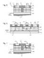
- the figure 1 illustrates an integrated circuit 4 including on the one hand two zones 4A and 4B comprising memory cells of the SRAM type and, on the other hand, zones 4C and 4D comprising logic gates. These different zones 4A to 4D are made on the same silicon substrate 401.
- the figure 2 is a schematic sectional view of the area 4D at a box layer.
- the 4D zone notably comprises transistors each comprising a gate stack. These transistors are typically of the FDSOI type.
- the transistors of the 4D zone are arranged in a manner known per se on a layer of ultra-fine buried insulation (typically designated by the acronym FDSOI).
- the buried insulating layer is provided on a ground plane layer.
- the ground plane layer is provided on a box layer.
- the caisson layer is provided on a deeply buried N-type caisson layer (referred to as deep n-well) in the English language.
- the N-type deep buried caisson layer is itself formed on the silicon substrate 401, which is typically P-doped.
- Each row contains transistors of the same type, isolated by isolation trenches.
- the adjacent rows form an alternation of nMOS and pMOS transistors.
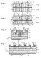
- the Figures 3 to 7 illustrate an example of a possible structure of the 4D zone.
- the Figures 3 to 7 are different sectional views at a group of transistors belonging to adjacent rows and / or having ground planes whose dopings are of opposite types.
- the illustrated transistor group has pMOS transistors in a first row and has nMOS transistors in an adjacent second row.
- the sources, drains and gates of the transistors are formed in and / or on a semiconductor active layer, the semiconductor layer being formed on a buried insulating layer. These transistors are of the FDSOI type.
- the first row and the second row are separated by an isolation trench 46.
- the first row comprises a transistor p1 and a transistor p2.
- Transistors p1 and p2 are separated by an isolation trench (not shown) in the thickness of the semiconductor active layer.
- the second row comprises a transistor n1 and a transistor n2.
- the transistors n1 and n2 are separated by an isolation trench 49 in the thickness of the semiconductor active layer.
- the isolation trench 49 also separates the transistor p1 from the interconnection vp1 in the thickness of the semiconductor active layer.
- the figure 3 is a sectional view from above of the area 4D at its wl box layer.
- the figure 4 is a sectional view from above of the area 4D at its ground plane layer gpl.
- the figure 5 is a side sectional view of the zone 4D at the level of interconnections vp1 and vn1 VIA type.
- the figure 6 is a front sectional view of the 4D area at the row of nMOS transistors.
- the figure 7 is a side sectional view of the 4D area at an active layer of transistors.
- interconnections vp1 and vn1 have been represented in dashed projection on the Figures 3 and 4 .
- the delineation of the active layer of the different transistors has been represented in projection on the Figures 3 and 4 .
- Type VIA interconnects vn1 and vp1 are formed through the semiconductor active layer.
- the interconnection vp1 is intended to bias the ground planes of the pMOS transistors.
- the interconnection vn1 is intended to bias the ground planes of the nMOS transistors.
- a VIA-type interconnection generally designates a conductive junction formed in a through-hole of different silicon layers. Such interconnections are thus usually integrated in order to achieve inter-layer interconnection within the integrated circuit.
- the caisson layer w1 has two semiconductor zones separated by the isolation trench 46.
- the two semiconducting zones comprise a P-type doping.
- the wp1, wp2, wn1 and wn2 caisson parts respectively arranged vertically. transistors p1, p2, n1 and n2 thus have the same P-type doping.
- the wt box part is arranged in line with a repetition cell (for Well Tap in English language) including the interconnections vp1 and vn1.
- the ground plane layer lpg has two semiconductor zones separated by the isolation trench 46.
- the two semiconductor zones comprise a P-type doping over their entire surface, with the exception of the plane zones.
- of mass gpp1 and gpn2 arranged vertically above the transistors p1 and n2.
- the ground plane regions gpp1 and gpn2 thus have N-type doping.
- the ground plane regions gpp2 and gpn1 thus exhibit P-type doping.
- the bpt ground plane region is disposed vertically above the cell. of repetition including the interconnections vp1 and vn1.
- the interconnection vn1 extends in depth up to the contact of the ground plane layer gp1, on a p-doped area gp1-p.
- the interconnection vp1 extends in depth up to the contact of the ground plane layer. mass gpl, on a p-doped gpl-p zone.
- An unillustrated polarization circuit applies bias voltages on the interconnects vp1 and vn1.
- the box layer w1 is separated from the sub substrate by means of a deep-buried doped N-type caisson dnw, in order to be able to apply a different polarization to the ground planes and the sub substrate.
- the substrate sub is biased at a voltage Vdds.
- the isolation trench 46 extends in depth to the deep buried caisson dnw to provide isolation between the rows of transistors.
- Insulation trenches 48 delineate the row of pMOS transistors relative to an adjacent pMOS transistors row, and the row of nMOS transistors relative to an adjacent nMOS transistors row. The isolation trenches 48 provide insulation between these adjacent rows in the thickness of the semiconductor active layer.
- the polarization of the ground plane gpp1 is carried out by the interconnection vp1 via the ground plane region gp1-p and via the caisson layer w1, forming a p-doped semiconductor path.
- Polarization of the ground plane gpp2 is performed by the interconnection vp1 via the ground plane region gp1-p forming a doped semiconductor path P.
- the polarization of the ground plane gpn1 is performed by the interconnection vn1 via the ground plane region gp1-p and through the box layer w1 forming a p-doped semiconductor path.
- the polarization of the ground plane gpn2 is effected by the interconnection vn1 by via the gpl-p ground plane region forming a P-doped semiconductor path.
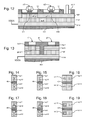
- the Figures 8 to 13 illustrate a first structural variant of the 4D zone according to the invention, to optimize its operation.
- the Figures 8 to 13 are different sectional views at a group of transistors belonging to adjacent rows and / or having ground planes whose dopings are of opposite types.
- the group of transistors illustrated has pMOS transistors in a first row and has nMOS transistors in a second row. adjacent. Repeating cells are arranged at regular intervals in the rows.
- the sources, drains and gates of the transistors are formed in and / or on a semiconductor active layer, the semiconductor layer being formed on a buried insulating layer.
- the insulating layer may advantageously be of so-called ultra-thin thickness, typically between 10 and 50 nm.
- These transistors are of the FDSOI type.
- the active silicon layer of an nMOS transistor comprises an N-doped source, a channel, and an N-doped drain.
- the active silicon layer of a pMOS transistor comprises a P-doped source, a channel, and a P-doped drain.
- the channel is covered by a gate oxide layer.
- the gate oxide is surmounted by a gate stack comprising a metal layer and a polysilicon layer. The stack is delimited laterally by spacers.
- the first row and the second row are separated by an isolation trench 46.
- the first row comprises a transistor p1 and a transistor p2.
- Transistors p1 and p2 are separated by an isolation trench (not shown) in the thickness of the semiconductor active layer.
- the second row comprises a transistor n1 and a transistor n2.
- the transistors n1 and n2 are separated by an isolation trench 49 in the thickness of the semiconductor active layer.
- the figure 8 is a sectional view from above of the area 4D at its wl box layer.
- the figure 9 is a sectional view from above of the area 4D at its ground plane layer gpl.
- the figure 10 is a side sectional view of the zone 4D at the level of interconnections vp11, vp12, vn11 and vn12 VIA type.
- the figure 11 is a front sectional view of the area 4D at the row of nMOS transistors and the interconnection vn11.
- the figure 12 is a front sectional view of the area 4D at the row of nMOS transistors and the vn12 interconnection.
- the figure 13 is a side sectional view of the 4D area at an active layer of transistors.
- the type VIA interconnections vp11, vp12, vn11 and vn12 are formed through the semiconductor active layer and the buried insulating layer.
- the interconnections vp11 and vp12 are intended to polarize the ground planes of the pMOS transistors.
- the interconnections vn11 and vn12 are intended to polarize the ground planes of the nMOS transistors.
- the box layer w1 has two semiconductor zones separated by the isolation trench 46.
- the two semiconducting zones comprise a P-type doping.
- the box areas wp1, wp2, wn1 and wn2 disposed respectively at the plumb transistors p1, p2, n1 and n2 comprise Thus, the same type of p-type doping.
- the box zone wt is disposed vertically above a repetition cell including the interconnections vp11, vp12, vn11 and vn12.
- the ground plane layer lpg has two semiconductor zones separated by the isolation trench 46.
- the two semiconductor zones comprise an N-type doping over their entire surface, with the exception of the plane zones.
- of mass gpp2 and gpn1 arranged vertically above the transistors p2 and n1.
- the ground plane regions gpp2 and gpn1 thus exhibit P-type doping and form as islands in a n-doped gpl-n ground plane region.
- the ground plane regions gpp1 and gpn2 thus exhibit N-type doping.
- the ground plane area bpt is disposed vertically above the repetition cell including the interconnects vp11, vp12, vn11 and vn12.
- the ground planes make it possible to improve the electrostatic control of the transistors by limiting the penetration of the electric fields generated by the drain and the source under the channel. Reduction of lateral electrostatic coupling reduces short channel effects and limits the effect of depletion by the drain (DIBL effect).
- the interconnections vp12 and vn11 extend in depth up to the contact of the ground plane layer gpl, on a p-doped gp1-p area.
- the interconnections vp11 and vn12 extend in depth up to the contact of the ground layer. gpl-ground plane, on an N-doped gpl-n region.
- An unillustrated bias circuit applies bias voltages on the interconnects vp11, vp12, vn11 and vn12. A same bias voltage is applied on the interconnections vp11 and vp12. A same bias voltage is applied on the interconnections vn11 and vn12.
- the bias voltage of the interconnection vp11 may be different from the bias voltage of the interconnection vin11.
- the box layer w1 is separated from the sub substrate by means of a deep-buried doped N-type casing dnw, in order to be able to apply a different polarization to the ground planes and to the substrate sub without the risk of creating a conductive pn junction. parasite.
- the deeply buried caisson dnw is biased at a voltage Vdds.
- the isolation trench 46 extends in depth to the deep buried caisson dnw.
- the isolation trench 46 and the deep buried caisson dnw provide insulation between the rows of nMOS and pMOS transistors.
- Insulation trenches 48 delineate the row of pMOS transistors relative to an adjacent pMOS transistors row, and the row of nMOS transistors relative to an adjacent nMOS transistors row.
- the isolation trenches 48 provide insulation between these adjacent rows in the thickness of the semiconductor active layer.
- the polarization of the ground plane gpp1 is carried out by the interconnection vp11 via the ground plane region gpl-n forming an N-doped semiconductor path.
- the polarization of the ground plane gpp2 is achieved by the interconnection vp12 through the ground plane region gp1-p and the box layer w1, forming a p-doped semiconductor path.
- the polarization of the ground plane gpn1 is performed by the interconnection vn11 via the ground plane region gp1-p and via the box layer w1, forming a p-doped semiconductor path.
- the polarization of the ground plane gpn2 is carried out by the interconnection vn12 via the gpl-n ground plane region forming an N-doped semiconductor path
- each ground plane of the transistors by a semiconductor path having the same type of doping, even when these transistors are separated from the interconnections by isolation trenches present in the active layer of semiconductor. This is feasible even for rows comprising transistors whose ground planes have doping of opposite types. Such a result is further obtained by means of a simple structure, with a box layer having the same type of doping for rows of nMOS transistors and rows of pMOS transistors.
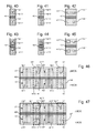
- the Figures 14 to 19 illustrate different variants of standard cells for the repetition cells, intended for the design of the topology of the integrated circuit 4, as defined in the example of the Figures 8 and 9 .
- the Figures 14 and 17 illustrate a first design variant of a repetition cell.
- the figure 14 corresponds to the section of this repetition cell at the level of the caisson layer.
- the figure 17 corresponds to the section of this repetition cell at the ground plane layer.
- the interconnections vp11, vp12 or vn11, vn12 use a common layer of active over a grid step width (illustrated by the line connecting the interconnections shown in projection).
- This variant corresponds to the example implemented in Figures 8 to 13 .
- the Figures 15 and 18 illustrate a second alternative design of a repetition cell.
- the figure 15 corresponds to the section of this repetition cell at the level of the caisson layer.
- the figure 18 corresponds to the section of this repetition cell at the ground plane layer.
- the interconnects vp11, vp12 or vn11, vn12 use a separate layer or zone of active over a grid step width.
- the Figures 16 and 19 illustrate a third design variant of a repetition cell.
- the figure 16 corresponds to the section of this repetition cell at the level of the caisson layer.
- the figure 18 corresponds to the section of this repetition cell at the ground plane layer.
- the interconnects vp11, vp12, or vn11, vn12 use a separate layer of active over twice the grid step width.
- the Figures 20 to 25 illustrate a second structural variant of the 4D zone according to the invention, to optimize its operation.
- the Figures 20 to 25 are different sectional views at a group of transistors belonging to adjacent rows and / or having ground planes whose dopings are of opposite types. This second variant requires a lower precision of the manufacturing process for doping the different areas of the ground plane layer.
- the group of transistors illustrated comprises pMOS transistors p1 and p2 separated by an isolation trench 49 in a first row and includes nMOS transistors n1 and n2 separated by an isolation trench in an adjacent second row, the rows being separated by the isolation trench 46.
- the sources, drains and grids of the transistors are formed in and / or on a semiconductor active layer, the semiconductor layer being formed on a buried insulating layer. These transistors are of the FDSOI type.
- the figure 20 is a sectional view from above of the area 4D at its wl box layer.
- the figure 21 is a sectional view from above of the area 4D at its ground plane layer gpl.
- the figure 22 is a front sectional view of the area 4D at a row of pMOS transistors, at the interconnection vp11.
- the figure 23 is a front sectional view of the area 4D at a row of pMOS transistors, at the interconnection vp12.
- the figure 24 is a side sectional view of the area 4D at the interconnections vp11, vp12 and vn1 type VIA.
- the figure 25 is a side sectional view of the 4D area at an active layer of transistors.
- the type VIA interconnections vp11, vp12, vp1, vn1, vn11 and vn12 are provided through the semiconductor active layer and the buried insulating layer.
- the box layer w1 has two semiconductor zones separated by the isolation trench 46.
- the two semiconducting zones comprise a P-type doping.
- the box areas wp1, wp2, wn1 and wn2 placed in line respectively transistors p1, p2, n1 and n2 thus have the same P-type doping.
- the box area wt1 is disposed in line with a repetition cell including the interconnections vp1, vn11 and vn12.
- the box area wt1 is arranged between the box areas wp1 and WP2.
- the caisson zone wt2 is placed in line with a repetition cell including the interconnections vn1, vp11 and vp12.
- the ground plane layer lpg has two semiconductor regions separated by the isolation trench 46.
- the ground plane region bpt1 is disposed vertically above the repetition cell including the interconnects vp1, vn11 and vn12.
- the ground plane area bpt2 is disposed vertically above the repetition cell including the interconnects vn1, vp11 and vp12.
- the ground plane layer gpl comprises a P-type doping.
- the ground plane layer gpl has an N-type doping.
- the ground plane layer gpl comprises a P-type doping.
- the ground plane layer gp1 comprises an N-type doping.
- the ground plane layer gpl comprises a P-type doping.
- the interconnections vp1, vn11 and vp12 extend in depth up to the contact of the ground plane layer gp1, on a p-doped area gp1-p.
- the interconnections vn1, vn12 and vp11 extend in depth up to the contact of the ground plane layer gpl, on a n-doped gpl-n region.
- An unillustrated bias circuit applies bias voltages on the interconnects vp1, vp11, vp12, vn1, vn11 and vn12. A same bias voltage is applied on the interconnections vp1, vp11 and vp12. A same bias voltage is applied on the interconnections vn1, vn11 and vn12.
- the bias voltage of the interconnection vp1 may be distinct from the bias voltage of the interconnection vn1.
- the box layer w1 is separated from the sub substrate by means of a deep-buried doped N-type caisson dnw.
- the deeply buried caisson is biased at a voltage Vdds.
- the isolation trench 46 extends in depth to the deep buried caisson dnw.
- the polarization of the ground plane gpp1 is carried out by the interconnection vp12 via the ground plane region gp1-p and the ground plane layer w1, forming a P-doped semiconductor path (and so redundant via the interconnection vp1 via the ground plane region gp1-p forming a doped semiconductor path P).
- the polarization of the ground plane gpp2 is performed by the interconnection vp11 via the ground plane region gp1-n forming an N-doped semiconductor path.
- Polarization of the ground plane gpn1 is performed by the interconnection vn12 via the ground plane region gpl-n.
- the polarization of the ground plane gpn2 is performed by the interconnection vn11 and the interconnection vn1 via the ground plane region gp1-p.
- the interconnections vp1, vp12 and vn1, vn11 provide a polarization redundancy of their respective box. Less polarization homogeneity would also be achieved by removing the interconnections vp12 and vn11 while allowing satisfactory operation of the integrated circuit. Such a deletion would facilitate in particular the manufacturing process of the integrated circuit.
- the Figures 26 to 37 illustrate different variants of standard cells for the repetition cells, intended for the design of the topology of the integrated circuit 4, as defined in the example of the Figures 20 and 21 .
- the Figures 26 and 30 illustrate a first design variant of a repetition cell.
- the figure 26 corresponds to the section of this repetition cell at the level of the caisson layer.
- the figure 30 corresponds to the section of this repetition cell at the ground plane layer.
- the interconnections vp11 and vp12 use a common layer of active over a grid step width (illustrated by the line connecting the interconnections represented in projection).
- This variant corresponds to the example implemented in Figures 20 to 25 .
- the Figures 27 and 31 illustrate a complement of the first design variant of a repetition cell.
- the figure 27 corresponds to the section of this repetition cell at the level of the caisson layer.
- the figure 31 corresponds to the section of this repetition cell at the ground plane layer.
- the vn11 and vn12 interconnects use a common layer of active over a grid step width. This variant corresponds to the example implemented in Figures 20 to 25 .
- the Figures 28 and 32 illustrate a second alternative design of a repetition cell.
- the figure 28 corresponds to the section of this repetition cell at the level of the caisson layer.
- the figure 32 corresponds to the section of this repetition cell at the ground plane layer.
- the interconnects vp11 and vp12 use a distinct layer of active over a grid step width.
- the doping of the ground plane and caisson layers are identical to those of the variant of Figures 26 and 30 .
- the Figures 29 and 33 illustrate a complement of the second design variant of a repetition cell.
- the figure 29 corresponds to the section of this repetition cell at the level of the caisson layer.
- the figure 33 corresponds to the section of this repetition cell at the ground plane layer.
- the vn11 and vn12 interconnects use a distinct layer of active over a grid step width.
- the doping of the ground plane and caisson layers are identical to those of the variant of Figures 27 and 31 .
- the Figures 34 and 36 illustrate a third design variant of a repetition cell.
- the figure 34 corresponds to the section of this repetition cell at the level of the caisson layer.
- the figure 36 corresponds to the section of this repetition cell at the ground plane layer.
- the interconnects vn1, vp11, and vp12 use a separate layer of active over twice the grid step width.
- the Figures 35 and 37 illustrate a complement of the third design variant of a repetition cell.
- the figure 35 corresponds to the section of this repetition cell at the level of the caisson layer.
- the figure 37 corresponds to the section of this repetition cell at the ground plane layer.
- the interconnects vp1, vn11 and vn12 use a distinct layer of active over a grid step width.
- the Figures 38 and 39 illustrate a third variant of integrated circuit structure according to the invention, to optimize its operation.
- the Figures 38 and 39 are sectional views from above at a group of transistors belonging to adjacent rows and / or having ground planes whose dopings are of opposite types.
- the figure 38 is a sectional view of the structure at its wl box layer.
- the figure 39 is a sectional view from above of the structure at its ground plane layer gpl.
- the group of transistors illustrated includes pMOS transistors p1 and p2 separated by an isolation trench in a first row and includes nMOS transistors n1 and n2 separated by an isolation trench 49 in an adjacent second row, the rows being separated by the isolation trench 46.
- the sources, drains and grids of the transistors are formed in and / or on a semiconductor active layer, the semiconductor layer being formed on a buried insulating layer. These transistors are of the FDSOI type.
- the structure has interconnections vp11, vp12, vn11 and vn12 VIA type.
- the type VIA interconnections vp11, vp12, vn11 and vn12 are formed through the semiconductor active layer and the buried insulating layer.
- the caisson layer w1 has two semiconductor zones separated by the isolation trench 46.
- the semiconductor zone perpendicular to the nMOS transistors comprises a P-type doping.
- the semiconducting zone is in line with the transistors.
- pMOS comprises an N-type doping.
- the box regions wp1 and wp2 disposed vertically above the transistors p1 and p2 respectively comprise the same type N doping.
- the box areas wn1 and wn2 are arranged vertically above the Transistors n1 and n2 thus have the same P-type doping.
- the box area wt is disposed vertically above a repetition cell including the interconnections vp11, vp12, vn11 and vn12.
- the ground plane layer lpg has two semiconductor regions separated by the isolation trench 46.
- the ground plane area bpt is disposed vertically above the repetition cell including the interconnections vp11, vp12, vn11 and vn12. .
- the semiconductor zone corresponding to the nMOSs comprises a P-type doping over its entire surface, with the exception of the ground plane region gpp1 disposed directly above the transistor p1 (which forms an island in a p-doped ground plane gpl-p).
- the ground plane region gpp2 thus exhibits P-type doping.
- the semiconductor zone corresponding to the pMOSs comprises N-type doping over its entire surface, with the exception of the ground plane region gpn1 arranged plumb with transistor n1 (which forms an island in a n-doped gpl-n ground plane region).
- the ground plane region gpn2 thus has N-type doping.
- the interconnections vp11 and vn12 extend in depth up to the contact of the ground plane layer gp1, on a p-doped area gp1-p.
- the interconnections vn12 and vp11 extend in depth up to the contact of the ground layer. gpl-ground plane, on an N-doped gpl-n region.
- An unillustrated bias circuit applies bias voltages on the interconnects vp11, vp12, vn11 and vn12. A same bias voltage is applied on the interconnections vp11 and vp12. A same bias voltage is applied on the interconnections vn11 and vn12.
- the bias voltage of the interconnection vp11 may be distinct from the bias voltage of the interconnection vn11.
- the box layer w1 is separated from the sub substrate by means of a deep-buried doped N-type caisson dnw.
- the deeply buried caisson is biased at a voltage Vdds.
- the isolation trench 46 extends in depth to the deep buried caisson dnw.
- the polarization of the ground plane gpp2 is carried out by the interconnection vp11 via the ground plane region gpl-p doped P.
- the polarization of the ground plane gpp1 is carried out by the interconnection vp12 by via the gpl-n region of the ground plane layer and via the N-doped well, thereby forming an N-doped semiconductor path.
- the polarization of the ground plane gpn2 is carried out by the interconnection vn12 via the region of ground plane gpl-n doped N.
- the polarization of the ground plane gpn1 is carried out by the interconnection vn11 via the gpl-p region of the ground plane layer and through the P-doped well, thus forming a P-doped semiconductor path.
- the Figures 40 to 45 illustrate different variants of standard cells for the repetition cells, intended for the design of the topology of the integrated circuit 4, as defined in the example of the Figures 38 and 39 .
- the Figures 40 and 43 illustrate a first design variant of a repetition cell.
- the figure 40 corresponds to the section of this repetition cell at the level of the caisson layer.
- the figure 43 corresponds to the section of this repetition cell at the ground plane layer.
- the interconnections vp11, vp12 or vn11, vn12 use a common layer of active over a grid step width (illustrated by the line connecting the interconnections shown in projection).
- This variant corresponds to the example implemented in Figures 38 and 39 .
- the Figures 41 and 44 illustrate a second alternative design of a repetition cell.
- the figure 41 corresponds to the section of this repetition cell at the level of the caisson layer.
- the figure 44 corresponds to the section of this repetition cell at the ground plane layer.
- the interconnects vp11, vp12 or vn11, vn12 use a separate layer or zone of active over a grid step width.
- the Figures 42 and 45 illustrate a third design variant of a repetition cell.
- the figure 42 corresponds to the section of this repetition cell at the level of the caisson layer.
- the figure 45 corresponds to the section of this repetition cell at the ground plane layer.
- the interconnects vp11, vp12, or vn11, vn12 use a separate layer of active over twice the grid step width.
- the Figures 46 and 47 illustrate a fourth variant of integrated circuit structure according to the invention, to optimize its operation.
- the Figures 46 to 47 are sectional views from above at the level of a group of transistors belonging to adjacent rows and / or having ground planes whose dopings are of opposite types.
- the figure 46 is a sectional view of the structure at its wl box layer.
- the figure 47 is a sectional view from above of the structure at its ground plane layer gpl.
- the group of transistors illustrated has pMOS transistors p1 and p2 separated by an isolation trench in a first row and includes nMOS transistors n1 and n2 separated by an isolation trench in an adjacent second row, the rows being separated by the isolation trench 46.
- the sources, drains and gates of the transistors are formed in and / or on a semiconductor active layer, the semiconductor layer being formed on a buried insulating layer. These transistors are of the FDSOI type.
- the structure has interconnects vp1, vp11, vp12, vn1, vn11 and vn12 VIA type.
- the VIA type interconnects vp1, vp11, vp12, vn1, vn11 and vn12 are formed through the semiconductor active layer and the buried insulating layer.
- the semiconductor zone plumb with the nMOS transistors comprises a p-type doping.
- the semiconductor region plumb with the pMOS transistors comprises an N-type doping.
- the wp1 and wp2 box areas are arranged vertically. respectively transistors p1 and p2 thus have the same type of N-doping.
- the box area wt1 is arranged in line with a repetition cell including the interconnections vp11, vp12, vn11 and vn12.
- the box area wt1 is disposed between the box areas wp1 and wp2.
- the box area wt2 is placed in line with a repetition cell including the interconnections vp1 and vn1.
- the ground plane layer lpg has two semiconductor zones separated by the isolation trench 46.
- the ground plane region bpt1 is disposed vertically above the repetition cell including the interconnections vp11, vp12, vn11 and vn12 .
- the ground plane area bpt2 is disposed vertically above the repetition cell including the interconnections vn1 and vp1.
- the ground plane layer gpl comprises a P-type doping.
- the ground plane layer gpl comprises an N-type doping.
- the ground plane layer gpl In line with the interconnections vp11 (arranged between the transistors p1 and p2) and vn12 (arranged between the transistors n1 and n2), over the entire width of their standard cell, the ground plane layer gpl has an N-type doping. In line with the interconnections vp12 (arranged between the transistors p1 and p2) and vn11 (arranged between the transistors n1 and n2), over the entire width of their standard cell, the ground plane layer gpl comprises a P-type doping.
- the interconnections vn1, vn11 and vp12 extend in depth up to the contact of the ground plane layer gp1, on a p-doped gp1-p area.
- the interconnections vp1, vn12 and vp11 extend in depth up to the contact of the ground plane layer gpl, on a n-doped gpl-n region.
- An unillustrated bias circuit applies bias voltages on the interconnects vp1, vp11, vp12, vn1, vn11 and vn12. A same bias voltage is applied on the interconnections vp1, vp11 and vp12. A same bias voltage is applied on the interconnections vn1, vn11 and vn12.
- the bias voltage of the interconnection vp1 may be distinct from the bias voltage of the interconnection vn1.
- the box layer w1 is separated from the sub substrate by means of a deep-buried doped N-type caisson dnw.
- the deeply buried caisson is biased at a voltage Vdds.
- the isolation trench 46 extends in depth to the deep buried caisson dnw.
- the polarization of the ground plane gpp1 is carried out by the interconnection vp12 via the ground plane region gpl-p forming a p-doped semiconductor path.
- the polarization of the ground plane gpp2 is achieved by the interconnection vp1 through the ground plane region gpl-n forming an N-doped semiconductor path.
- the polarization of the ground plane gpp2 is redundantly performed by the interconnection vp11 via the plane region mass gpl-n, which further ensures a polarization redundancy of the box layer in line with the pMOS transistors. The homogeneity of the polarization of the box layer is thus increased.
- the polarization of the ground plane gpn1 is carried out by the interconnection vn12 via the ground plane region gpl-n forming an N-doped semiconductor path.
- the polarization of the ground plane gpn2 is achieved by the interconnection vn1 via the ground plane region gp1-p forming a p-doped semiconductor path.
- the polarization of the ground plane gpn2 is performed redundantly by the vn11 interconnection via the plan area. of mass gpl-p, which further allows to provide a polarization redundancy of the box layer in line with nMOS transistors. The homogeneity of the polarization of the box layer is thus increased.
- a direct polarization of the ground plane of a transistor is carried out by a direct semiconductor path having the same type of doping.
- the Figures 48 to 53 illustrate different variants of standard cells for the repetition cells, intended for the design of the topology of the integrated circuit 4, as defined in the example of the Figures 46 and 47 .
- the Figures 48 and 51 illustrate a first design variant of a repetition cell.
- the figure 48 corresponds to the section of this repetition cell at the level of the caisson layer.
- the figure 51 corresponds to the section of this repetition cell at the ground plane layer.
- the interconnections vp11, vp12 or vn11, vn12 use a common layer of active over a grid step width (illustrated by the line connecting the interconnections shown in projection).
- This variant corresponds to the example implemented in Figures 46 and 47 .
- the Figures 49 and 52 illustrate a second alternative design of a repetition cell.
- the figure 49 corresponds to the section of this repetition cell at the level of the caisson layer.
- the figure 52 corresponds to the section of this repetition cell at the ground plane layer.
- the interconnects vp11, vp12 or vn11, vn12 use a separate layer or zone of active over a grid step width.
- the Figures 50 and 53 illustrate a third design variant of a repetition cell.
- the figure 50 corresponds to the section of this repetition cell at the level of the caisson layer.
- the figure 53 corresponds to the section of this repetition cell at the ground plane layer.
- the interconnects vp11, vp12, or vn11, vn12 use a separate layer of active over twice the grid step width.
- the Figures 54 and 55 illustrate a variation of the fourth variant of integrated circuit structure according to the invention, to simplify its structure.
- the Figures 54 and 55 are sectional views from above at a group of transistors belonging to adjacent rows and / or having ground planes whose dopings are of opposite types.
- the figure 54 is a sectional view of the structure at its wl box layer.
- the figure 55 is a sectional view from above of the structure at its ground plane layer gpl.
- the repetition cell placed between the transistors p1 and p2 comprises simplified culture.
- This repetition cell comprises only an interconnection vp1 for the transistor p1, and an interconnection vn1 for the transistor n1.
- the ground plane area bpt1 disposed vertically above the repetition cell comprises a P-type doping between the transistors p1 and p2, and an N-type doping between the transistors n1 and n2.
- the box layer perpendicular to the pMOS transistors is here polarized solely via the bpt2 zone of the repetition cell including the interconnection vp1.
- the box layer directly above the nMOS transistors is here polarized only via the zone bpt2 of the repetition cell including the interconnection vn1.
- the polarization of the box layer w1 may be less homogeneous than in the example of Figures 46 and 47 this homogeneity may be sufficient while facilitating the manufacturing process of the integrated circuit.
Abstract
Description
L'invention concerne les circuits intégrés, et en particulier les circuits intégrés réalisés sur un substrat de type silicium sur isolant (SOI). La technologie SOI consiste à séparer une fine couche de silicium (quelques nanomètres) sur un substrat en silicium par une couche d'isolant relativement épaisse (quelques dizaines de nanomètres en règle générale).The invention relates to integrated circuits, and in particular integrated circuits made on a silicon-on-insulator (SOI) type substrate. SOI technology consists of separating a thin layer of silicon (a few nanometers) on a silicon substrate by a relatively thick insulating layer (a few tens of nanometers as a rule).
Les circuits intégrés réalisés en technologie SOI présentent un certain nombre d'avantages. De tels circuits présentent généralement une plus faible consommation électrique en statique et en dynamique pour des performances équivalentes, grâce à un meilleur contrôle électrostatique du canal par la grille. Du fait d'un canal non dopé, les dispersions des caractéristiques électriques sont également plus faibles. De tels circuits induisent également des capacités parasites plus faibles, qui permettent d'améliorer la vitesse de commutation. De plus, le phénomène de déclenchement parasite (latchup en langue anglaise) rencontré par les transistors MOS en technologie Bulk peut être évité au profit de la robustesse de fonctionnement, du fait de la présence de la couche d'oxyde isolante. De tels circuits s'avèrent donc particulièrement adaptés pour des applications de type SoC. On constate également que les circuits intégrés SOI sont moins sensibles aux effets des radiations ionisantes et s'avèrent ainsi plus fiables dans des applications où de telles radiations peuvent induire des problèmes de fonctionnement, notamment dans des applications spatiales. Les circuits intégrés SOI peuvent notamment comprendre des mémoires vives de type SRAM ou des portes logiques. La réalisation des circuits intégrés SOI reste en outre relativement semblable à celle de la technologie Bulk.Integrated circuits made in SOI technology have a number of advantages. Such circuits generally have a lower static and dynamic power consumption for equivalent performance, thanks to better electrostatic control of the channel by the gate. Due to an undoped channel, the dispersions of the electrical characteristics are also lower. Such circuits also induce lower parasitic capacitances, which make it possible to improve the switching speed. In addition, the phenomenon of parasitic triggering (latchup in English language) encountered by the MOS transistors Bulk technology can be avoided in favor of the robustness of operation, due to the presence of the insulating oxide layer. Such circuits are therefore particularly suitable for applications of SoC type. It can also be seen that the SOI integrated circuits are less sensitive to the effects of ionizing radiation and thus prove more reliable in applications where such radiations can induce operating problems, especially in space applications. The SOI integrated circuits can notably comprise SRAM-type random access devices or logic gates. The realization of the SOI integrated circuits also remains relatively similar to that of the Bulk technology.
La réduction de la consommation statique de portes logiques tout en augmentant leur vitesse de basculement fait l'objet de nombreuses recherches. Certains circuits intégrés en cours de développement intègrent à la fois des portes logiques à faible consommation et des portes logiques à vitesse de basculement élevée. Pour générer ces deux types de portes logiques sur un même circuit intégré, on choisit des portes logiques à accès rapide ou des portes logiques à faible consommation dans des bibliothèques de portes logiques. En technologie Bulk, la modulation du niveau de tension de seuil de transistors de même type est effectuée en différenciant le niveau de dopage de leur canal. Cependant, en technologie FDSOI (pour Fully Depleted Silicium On Insulator en langue anglaise, désignant du silicium totalement déserté sur isolant), le dopage du canal est quasiment nul. Ainsi, le niveau de dopage du canal des transistors ne peut donc pas présenter de variations importantes sans perdre les avantages associés, ce qui empêche de différencier les tensions de seuil en jouant sur ce dopage. Les tensions de seuils en technologie FDSOI à canal non dopé sont ainsi déterminées essentiellement par le travail de sortie de la grille. Un travail de sortie légèrement en dessous du milieu de la bande interdite (midgap), dit de type N, pour les nMOS, est généralement souhaité pour obtenir des tensions de seuil entre 0.2 et 0.5V. De manière symétrique, un travail de sortie légèrement au dessus du milieu de la bande interdite (midgap), dit de type P, pour les pMOS, est généralement souhaité pour obtenir des tensions de seuil entre -0.2 et -0.5V.Reducing the static consumption of logic gates while increasing their tipping speed is the subject of much research. Some integrated circuits under development integrate both low-power logic gates and logic gates with high failover speeds. To generate these two types of logic gates on the same integrated circuit, fast access logic gates or low power logic gates are chosen in logic gate libraries. In Bulk technology, the modulation of the threshold voltage level of transistors of the same type is performed by differentiating the doping level of their channel. However, in FDSOI (for Fully Depleted Silicon On Insulator in English, designating totally deserted silicon on insulator), the doping of the channel is virtually zero. Thus, the doping level of the channel of the transistors can not therefore present significant variations without losing the associated advantages, which makes it possible to differentiate voltages from threshold by playing on this doping. The threshold voltages in undoped channel FDSOI technology are thus essentially determined by the output work of the gate. An output work slightly below the mid-point (midgap), said N-type, for nMOS is generally desired to obtain threshold voltages between 0.2 and 0.5V. Symmetrically, an output job slightly above the mid-point (midgap), said P-type, for pMOS is generally desired to obtain threshold voltages between -0.2 and -0.5V.
Afin de disposer de tensions de seuil distinctes pour différents transistors en technologie FDSOI, il est également connu d'utiliser un plan de masse polarisé disposé entre une couche d'oxyde isolante mince et le substrat de silicium. En jouant sur le dopage des plans de masse et sur leur polarisation, on peut définir une gamme de tensions de seuil pour les différents transistors. On pourra ainsi disposer de transistors à faible tension de seuil dits LVT, de transistors à haute tension de seuil dits HVT et de transistors à tension de seuil moyenne dits SVT.In order to have distinct threshold voltages for different transistors in FDSOI technology, it is also known to use a polarized ground plane disposed between a thin insulating oxide layer and the silicon substrate. By playing on the doping of the ground planes and on their polarization, one can define a range of threshold voltages for the different transistors. It will thus be possible to have low threshold voltage transistors known as LVTs, so-called HVT high-voltage threshold transistors and SVT average threshold voltage transistors.
Les transistors d'un circuit intégré sont généralement disposés selon des doubles rangées alternées de nMOS et de pMOS. Une rangée de transistors nMOS est séparée d'une rangée de transistors pMOS par l'intermédiaire d'une tranchée d'isolation. Afin de disposer de transistors présentant des tensions de seuil différentes dans une même rangée, certains transistors sont ménagés à l'aplomb d'un plan de masse à dopage de type N, tandis que d'autres transistors sont ménagés à l'aplomb d'un plan de masse à dopage de type P.The transistors of an integrated circuit are generally arranged in alternating double rows of nMOS and pMOS. A row of nMOS transistors is separated from a row of pMOS transistors via an isolation trench. In order to have transistors with different threshold voltages in the same row, some transistors are arranged in line with an N-type doped ground plane, while other transistors are arranged in line with each other. a P-type doped ground plane.
Le document
On constate d'une part que le temps de diffusion de la polarisation à l'intérieur d'un plan de masse est relativement long, et d'autre part qu'une conception relativement complexe du circuit nécessaire pour éviter de former des diodes parasites conductrices entre les différents dopages des semiconducteurs en fonction de la polarisation qui leur est appliquée. Par ailleurs, il s'avère que la formation de contacts en vue de polariser les différents types de plans de masse s'avère complexe et implique l'utilisation d'une surface non négligeable de cellules de transition, au détriment de la densité d'intégration.On the one hand, it can be seen that the diffusion time of the polarization inside a ground plane is relatively long, and on the other hand that a relatively complex design of the circuit necessary to avoid forming conductive parasitic diodes between the different semiconductor dopings as a function of the polarization applied to them. Moreover, it appears that the formation of contacts in order to polarize the different types of ground planes proves to be complex and involves the use of a non-negligible surface of transition cells, to the detriment of the density of integration.
L'invention vise à résoudre un ou plusieurs de ces inconvénients. L'invention porte ainsi sur un circuit intégré comprenant un empilement d'un substrat semi-conducteur, d'une couche isolante enterrée et d'une couche semi-conductrice, comprenant :
- un premier composant électronique formé dans et/ou sur ladite couche semi-conductrice :
- un circuit de polarisation configuré pour générer une première tension de polarisation ;
- des première et deuxième interconnexions de type VIA, sur lesquelles le circuit de polarisation applique une même tension de polarisation égale à la première tension de polarisation ;
- au moins une première tranchée d'isolation séparant le premier composant électronique des première et deuxième interconnexions dans la couche semi-conductrice ;
- un premier plan de masse présentant un premier type de dopage, disposé sous la couche isolante enterrée à l'aplomb du premier composant électronique, et s'étendant sous la première tranchée d'isolation et jusqu'en contact avec la première interconnexion ;
- un premier caisson présentant un deuxième type de dopage opposé au premier type, disposé à l'aplomb du premier plan de masse, et s'étendant sous la première tranchée d'isolation et jusqu'en contact avec la deuxième interconnexion.
- a first electronic component formed in and / or on said semiconductor layer:
- a bias circuit configured to generate a first bias voltage;
- first and second type VIA interconnects, on which the bias circuit applies the same bias voltage equal to the first bias voltage;
- at least one first isolation trench separating the first electronic component from the first and second interconnections in the semiconductor layer;
- a first ground plane having a first type of doping, disposed beneath the insulating layer buried above the first electronic component, and extending under the first isolation trench and until contact with the first interconnection;
- a first box having a second type of doping opposed to the first type, placed in line with the first ground plane, and extending under the first isolation trench and until contact with the second interconnection.
Selon une variante, le circuit comprend en outre :
- un deuxième composant électronique formé dans et/ou sur ladite couche semi-conductrice :
- un deuxième plan de masse présentant le deuxième type de dopage, disposé à l'aplomb de la couche isolante enterrée à l'aplomb du deuxième composant électronique, le premier caisson s'étendant jusqu'en contact avec le deuxième plan de masse.
- a second electronic component formed in and / or on said semiconductor layer:
- a second ground plane having the second type of doping, disposed vertically above the insulating layer buried in line with the second electronic component, the first caisson extending to contact with the second ground plane.
Selon encore une variante, ledit premier caisson comporte une jonction présentant le deuxième type de dopage et s'étendant dans une même couche que les premier et deuxième plans de masse jusqu'à la deuxième interconnexion.According to another variant, said first box comprises a junction having the second type of doping and extending in the same layer as the first and second ground planes up to the second interconnection.
Selon une autre variante, les premier et deuxième composants électroniques sont des transistors FDSOI de même type nMOS ou pMOS.According to another variant, the first and second electronic components are FDSOI transistors of the same type nMOS or pMOS.
Selon encore une autre variante, les premier et deuxième transistors sont disposés dans une même rangée de transistors, le deuxième plan de masse étant entouré de semi-conducteur présentant le premier type de dopage dans la couche incluant les premier et deuxième plans de masse.According to yet another variant, the first and second transistors are arranged in the same row of transistors, the second ground plane being surrounded by semiconductor having the first type of doping in the layer including the first and second ground planes.
Selon une variante, les premier et deuxième transistors sont disposés dans une même rangée de transistors, le deuxième plan de masse s'étendant sur la largeur de la rangée.According to a variant, the first and second transistors are arranged in the same row of transistors, the second ground plane extending over the width of the row.
Selon encore une variante, le circuit comprend une jonction électrique connectant lesdites première et deuxième interconnexions dans la couche semi-conductrice, lesdites première et deuxième interconnexions étant ménagées dans une même cellule de répétition présentant une largeur d'un pas de grille du premier transistor.According to another variant, the circuit comprises an electrical junction connecting said first and second interconnections in the semiconductor layer, said first and second interconnections being formed in the same repetition cell having a gate width of the first transistor.
Selon une autre variante, le circuit ne comprend pas de jonction électrique connectant lesdites première et deuxième interconnexions dans la couche semi-conductrice, lesdites première et deuxième interconnexions étant ménagées dans une même cellule de répétition présentant une largeur d'un pas de grille du premier transistor.According to another variant, the circuit does not comprise an electrical junction connecting said first and second interconnections in the semiconductor layer, said first and second interconnections being formed in the same repetition cell having a gate pitch width of the first transistor.
Selon une autre variante, le circuit ne comprend pas de jonction électrique connectant lesdites première et deuxième interconnexions dans la couche semi-conductrice, lesdites première et deuxième interconnexions étant ménagées dans une même cellule de répétition présentant une largeur de deux pas de grille du premier transistor.According to another variant, the circuit does not comprise an electrical junction connecting said first and second interconnections in the semiconductor layer, said first and second interconnections being formed in the same repetition cell having a width of two grid pitches of the first transistor. .
Selon une autre variante, le circuit comprend en outre :
- un troisième transistor FDSOI d'un type opposé au premier transistor, formé dans et/ou sur ladite couche semi-conductrice ;
- un quatrième transistor FDSOI du même type que le troisième transistor et formé dans et/ou sur ladite couche semi-conductrice ;
- le circuit de polarisation étant configuré pour générer une deuxième tension de polarisation ;
- des troisième et quatrième interconnexions de type VIA, sur lesquelles le circuit de polarisation applique une même tension de polarisation égale à la deuxième tension de polarisation ;
- au moins une deuxième tranchée d'isolation séparant le troisième transistor des troisième et quatrième interconnexions dans la couche semi-conductrice ;
- un troisième plan de masse présentant un troisième type de dopage, disposé sous la couche isolante enterrée à l'aplomb du troisième transistor, et s'étendant sous la première tranchée d'isolation et jusqu'en contact avec la troisième interconnexion ;
- un deuxième caisson présentant un quatrième type de dopage opposé au troisième type, disposé à l'aplomb du troisième plan de masse, et s'étendant sous la première tranchée d'isolation et jusqu'en contact avec la quatrième interconnexion ;
- un quatrième plan de masse présentant le quatrième type de dopage, disposé à l'aplomb de la couche isolante enterrée à l'aplomb du quatrième transistor, le deuxième caisson s'étendant jusqu'en contact avec le quatrième plan de masse.
- a third FDSOI transistor of a type opposite to the first transistor, formed in and / or on said semiconductor layer;
- a fourth FDSOI transistor of the same type as the third transistor and formed in and / or on said semiconductor layer;
- the bias circuit being configured to generate a second bias voltage;
- third and fourth type VIA interconnects, on which the bias circuit applies the same bias voltage equal to the second bias voltage;
- at least one second isolation trench separating the third transistor from the third and fourth interconnections in the semiconductor layer;
- a third ground plane having a third type of doping disposed beneath the insulating layer buried in line with the third transistor, and extending under the first isolation trench and until contact with the third interconnection;
- a second box having a fourth type of doping opposed to the third type, disposed plumb with the third ground plane, and extending under the first isolation trench and until contact with the fourth interconnection;
- a fourth ground plane having the fourth type of doping, disposed vertically above the insulating layer buried above the fourth transistor, the second caisson extending to contact with the fourth ground plane.
Selon encore une variante, les premier et deuxième caissons présentent un même type de dopage.According to another variant, the first and second boxes have the same type of doping.
Selon encore une autre variante, ledit premier caisson est séparé du substrat par un caisson profondément enterré ménagé à l'aplomb du premier caisson.According to yet another variant, said first box is separated from the substrate by a deep buried box formed above the first box.
Selon une variante, ledit substrat présente un dopage de type P.According to a variant, said substrate has a P-type doping.
D'autres caractéristiques et avantages de l'invention ressortiront clairement de la description qui en est faite ci-après, à titre indicatif et nullement limitatif, en référence aux dessins annexés, dans lesquels :
- la
figure 1 illustre schématiquement une vue en coupe de dessus d'un circuit intégré au niveau des caissons ; - la
figure 2 est une vue en coupe schématique au niveau des caissons d'un premier exemple d'une zone d'intégration ; - les
figures 3 et 4 sont des vues de dessus en coupe d'une partie de zone d'intégration selon un développement envisageable mais non optimal, respectivement au niveau des caissons et des plans de masse ; - la
figure 5 est une vue en coupe de côté de la zone desfigures 3 et 4 au niveau d'une cellule de répétition ; - la
figure 6 est une vue en coupe de côté de la zone desfigures 3 et 4 au niveau d'une rangée de nMOS ; - la
figure 7 est une vue en coupe de côté de la zone desfigures 3 et 4 au niveau d'un transistor nMOS et d'un transistor pMOS adjacent ; - les
figures 8 et 9 sont des vues de dessus en coupe d'une partie d'une zone d'intégration selon une variante de l'invention, respectivement au niveau des caissons et des plans de masse ; - la
figure 10 est une vue en coupe de côté de la zone desfigures 8 et 9 au niveau d'une cellule de répétition ; - la
figure 11 est une vue en coupe de face de la zone desfigures 8 et 9 au niveau d'une rangée de nMOS ; - la
figure 12 est une autre vue en coupe de face de la zone desfigures 8 et 9 au niveau d'une rangée de nMOS ; - la
figure 13 est une vue en coupe de côté de la zone desfigures 8 et 9 au niveau d'un transistor nMOS et d'un transistor pMOS adjacent ; - les
figures 14 à 16 représentent différentes variantes de cellules de répétition en coupe au niveau du caisson ; - les
figures 17 à 19 représentent différentes variantes de cellules de répétition en coupe au niveau du plan de masse ; - les
figures 20 et 21 sont des vues de dessus en coupe d'une partie d'une autre variante de zone d'intégration, respectivement au niveau des caissons et des plans de masse ; - la
figure 22 est une vue en coupe de face de la zone desfigures 20 et 21 au niveau d'une rangée de pMOS ; - la
figure 23 est une autre vue en coupe de face de la zone desfigures 20 et 21 au niveau d'une rangée de pMOS ; - la
figure 24 est une vue en coupe de côté de la zone desfigures 20 et 21 au niveau d'une cellule de répétition ; - la
figure 25 est une vue en coupe de côté de la zone desfigures 20 et 21 au niveau d'un transistor nMOS et d'un transistor pMOS adjacent ; - les
figures 26 à 29 représentent différentes variantes de cellules de répétition en coupe au niveau du caisson ; - les
figures 30 à 33 représentent différentes variantes de cellules de répétition en coupe au niveau du plan de masse ; - les
figures 34 et 35 représentent différentes variantes de cellules de répétition en coupe au niveau du caisson ; - les
figures 36 et 37 représentent différentes variantes de cellules de répétition en coupe au niveau du plan de masse ; - les
figures 38 et 39 sont des vues de dessus en coupe d'une partie d'une autre variante de zone d'intégration, respectivement au niveau des caissons et des plans de masse ; - les
figures 40 à 42 représentent différentes variantes de cellules de répétition en coupe au niveau du caisson ; - les
figures 43 à 45 représentent différentes variantes de cellules de répétition en coupe au niveau du plan de masse ; - les
figures 46 et 47 sont des vues de dessus en coupe d'une partie d'une autre variante de zone d'intégration, respectivement au niveau des caissons et des plans de masse ; - les
figures 48 à 50 représentent différentes variantes de cellules de répétition en coupe au niveau du caisson ; - les
figures 51 à 53 représentent différentes variantes de cellules de répétition en coupe au niveau du plan de masse ; - les
figures 54 et 55 sont des vues de dessus en coupe d'une partie d'une autre variante de zone d'intégration, respectivement au niveau des caissons et des plans de masse.
- the
figure 1 schematically illustrates a top sectional view of an integrated circuit at the caissons; - the
figure 2 is a schematic sectional view at the caissons of a first example of an integration zone; - the
Figures 3 and 4 are top views in section of an integration zone part according to a possible but not optimal development, respectively at the caissons and the ground planes; - the
figure 5 is a side sectional view of the area ofFigures 3 and 4 at the level of a repetition cell; - the
figure 6 is a side sectional view of the area ofFigures 3 and 4 at a row of nMOS; - the
figure 7 is a side sectional view of the area ofFigures 3 and 4 at a nMOS transistor and an adjacent pMOS transistor; - the
Figures 8 and 9 are top views in section of a portion of an integration zone according to a variant of the invention, respectively at the caissons and ground planes; - the
figure 10 is a side sectional view of the area ofFigures 8 and 9 at the level of a repetition cell; - the
figure 11 is a front sectional view of the area ofFigures 8 and 9 at a row of nMOS; - the
figure 12 is another front sectional view of the area ofFigures 8 and 9 at a row of nMOS; - the
figure 13 is a side sectional view of the area ofFigures 8 and 9 at a nMOS transistor and an adjacent pMOS transistor; - the
Figures 14 to 16 represent different variants of repeat cells in section at the caisson; - the
Figures 17 to 19 represent different variants of repeat cells in section at the ground plane; - the
Figures 20 and 21 are sectional top views of a portion of another integration zone variant, respectively at the caissons and the ground planes; - the
figure 22 is a front sectional view of the area ofFigures 20 and 21 at a row of pMOS; - the
figure 23 is another front sectional view of the area ofFigures 20 and 21 at a row of pMOS; - the
figure 24 is a side sectional view of the area ofFigures 20 and 21 at the level of a repetition cell; - the
figure 25 is a side sectional view of the area ofFigures 20 and 21 at a nMOS transistor and an adjacent pMOS transistor; - the
Figures 26 to 29 represent different variants of repeat cells in section at the caisson; - the
Figures 30 to 33 represent different variants of repeat cells in section at the ground plane; - the
Figures 34 and 35 represent different variants of repeat cells in section at the caisson; - the
Figures 36 and 37 represent different variants of repeat cells in section at the ground plane; - the
Figures 38 and 39 are sectional top views of a portion of another integration zone variant, respectively at the caissons and the ground planes; - the
Figures 40 to 42 represent different variants of repeat cells in section at the caisson; - the
Figures 43 to 45 represent different variants of repeat cells in section at the ground plane; - the
Figures 46 and 47 are sectional top views of a portion of another integration zone variant, respectively at the caissons and the ground planes; - the
Figures 48 to 50 represent different variants of repeat cells in section at the caisson; - the
Figures 51 to 53 represent different variants of repeat cells in section at the ground plane; - the
Figures 54 and 55 are top views in section of a portion of another integration zone variant, respectively at the caissons and the ground planes.
La
La
Dans la zone 4D, on distingue une zone 42 dopée P et formant les caissons de rangées r1 à r6 de transistors. On distingue des contacts 414 destinés à polariser le caisson profondément enterré à dopage de type N. On distingue également des contacts 415 destinés à polariser les plans de masse des transistors aux extrémités des rangées r1 à r6.In the
On distingue une zone 46 formant des tranchées d'isolation profonde, isolant les rangées de transistors adjacentes jusqu'à la couche de caisson. Chaque rangée contient des transistors d'un même type, isolés par des tranchées d'isolation. Les rangées adjacentes forment une alternance de transistors nMOS et pMOS.There is a
Les
Le groupe de transistors illustré comporte des transistors pMOS dans une première rangée et comporte des transistors nMOS dans une seconde rangée adjacente. Les sources, drains et grilles des transistors sont ménagés dans et/ou sur une couche active semi-conductrice, la couche semi-conductrice étant ménagée sur une couche isolante enterrée. Ces transistors sont de type FDSOI. La première rangée et la seconde rangée sont séparées par une tranchée d'isolation 46. La première rangée comporte un transistor p1 et un transistor p2. Les transistors p1 et p2 sont séparés par une tranchée d'isolation (non illustrée) dans l'épaisseur de la couche active semi-conductrice. La deuxième rangée comporte un transistor n1 et un transistor n2. Les transistors n1 et n2 sont séparés par une tranchée d'isolation 49 dans l'épaisseur de la couche active semi-conductrice. La tranchée d'isolation 49 sépare également le transistor p1 de l'interconnexion vp1 dans l'épaisseur de la couche active semi-conductrice.The illustrated transistor group has pMOS transistors in a first row and has nMOS transistors in an adjacent second row. The sources, drains and gates of the transistors are formed in and / or on a semiconductor active layer, the semiconductor layer being formed on a buried insulating layer. These transistors are of the FDSOI type. The first row and the second row are separated by an
La
Dans un souci de lisibilité, les interconnexions vp1 et vn1 ont été représentées en projection en pointillé sur les
Des interconnexions de type VIA vn1 et vp1 sont ménagées à travers la couche active semi-conductrice. L'interconnexion vp1 est destinée à polariser les plans de masse des transistors pMOS. L'interconnexion vn1 est destinée à polariser les plans de masse des transistors nMOS.Type VIA interconnects vn1 and vp1 are formed through the semiconductor active layer. The interconnection vp1 is intended to bias the ground planes of the pMOS transistors. The interconnection vn1 is intended to bias the ground planes of the nMOS transistors.
Une interconnexion de type VIA désigne généralement une jonction conductrice ménagée dans un trou traversant différentes couches de silicium. De telles interconnexions sont ainsi usuellement intégrées afin de réaliser une interconnexion inter-couches à l'intérieur du circuit intégré.A VIA-type interconnection generally designates a conductive junction formed in a through-hole of different silicon layers. Such interconnections are thus usually integrated in order to achieve inter-layer interconnection within the integrated circuit.
La couche de caisson wl présente deux zones semi-conductrices séparées par la tranchée d'isolation 46. Les deux zones semi-conductrices comportent un dopage de type P. Les parties de caisson wp1, wp2, wn1 et wn2 disposées respectivement à l'aplomb des transistors p1, p2, n1 et n2 comportent ainsi un même dopage de type P. La partie de caisson wt est disposée à l'aplomb d'une cellule de répétition (pour Well Tap en langue anglaise) incluant les interconnexions vp1 et vn1.The caisson layer w1 has two semiconductor zones separated by the
La couche de plan de masse gpl présente deux zones semi-conductrices séparées par la tranchée d'isolation 46. Les deux zones semi-conductrices comportent un dopage de type P sur l'ensemble de leur surface, à l'exception des zones de plan de masse gpp1 et gpn2 disposées à l'aplomb des transistors p1 et n2. Les zones de plan de masse gpp1 et gpn2 présentent ainsi un dopage de type N. Les zones de plan de masse gpp2 et gpn1 présentent ainsi un dopage de type P. La zone de plan de masse bpt est disposée à l'aplomb de la cellule de répétition incluant les interconnexions vp1 et vn1.The ground plane layer lpg has two semiconductor zones separated by the
L'interconnexion vn1 s'étend en profondeur jusqu'au contact de la couche de plan de masse gpl, sur une zone gpl-p dopée P. L'interconnexion vp1 s'étend en profondeur jusqu'au contact de la couche de plan de masse gpl, sur une zone gpl-p dopée P. Un circuit de polarisation non illustré applique des tensions de polarisation sur les interconnexions vp1 et vn1.The interconnection vn1 extends in depth up to the contact of the ground plane layer gp1, on a p-doped area gp1-p. The interconnection vp1 extends in depth up to the contact of the ground plane layer. mass gpl, on a p-doped gpl-p zone. An unillustrated polarization circuit applies bias voltages on the interconnects vp1 and vn1.
La couche de caisson wl est séparée du substrat sub par l'intermédiaire d'un caisson profondément enterré à dopage de type N dnw, afin de pouvoir appliquer une polarisation différente aux plans de masse et au substrat sub. Dans l'exemple, le substrat sub est polarisé à une tension Vdds. La tranchée d'isolation 46 s'étend en profondeur jusqu'au caisson profondément enterré dnw afin d'assurer une isolation entre les rangées de transistors. Des tranchées d'isolation 48 délimitent la rangée des transistors pMOS par rapport à une rangée de transistors pMOS adjacente, et la rangée des transistors nMOS par rapport à une rangée de transistors nMOS adjacente. Les tranchées d'isolation 48 assurent une isolation entre ces rangées adjacentes dans l'épaisseur de la couche active semi-conductrice.The box layer w1 is separated from the sub substrate by means of a deep-buried doped N-type caisson dnw, in order to be able to apply a different polarization to the ground planes and the sub substrate. In the example, the substrate sub is biased at a voltage Vdds. The
La polarisation du plan de masse gpp1 est réalisée par l'interconnexion vp1 par l'intermédiaire de la zone de plan de masse gpl-p et par l'intermédiaire de la couche de caisson wl, formant un trajet semi-conducteur dopé P. La polarisation du plan de masse gpp2 est réalisée par l'interconnexion vp1 par l'intermédiaire de la zone de plan de masse gpl-p formant un trajet semi-conducteur dopé P. La polarisation du plan de masse gpn1 est réalisée par l'interconnexion vn1 par l'intermédiaire de la zone de plan de masse gpl-p et par l'intermédiaire de la couche de caisson wl, formant un trajet semi-conducteur dopé P. La polarisation du plan de masse gpn2 est réalisée par l'interconnexion vn1 par l'intermédiaire de la zone de plan de masse gpl-p formant un trajet semi-conducteur dopé P.The polarization of the ground plane gpp1 is carried out by the interconnection vp1 via the ground plane region gp1-p and via the caisson layer w1, forming a p-doped semiconductor path. Polarization of the ground plane gpp2 is performed by the interconnection vp1 via the ground plane region gp1-p forming a doped semiconductor path P. The polarization of the ground plane gpn1 is performed by the interconnection vn1 via the ground plane region gp1-p and through the box layer w1 forming a p-doped semiconductor path. The polarization of the ground plane gpn2 is effected by the interconnection vn1 by via the gpl-p ground plane region forming a P-doped semiconductor path.
Une telle structure présente cependant l'inconvénient de nécessiter un temps de polarisation non négligeable (pouvant atteindre plusieurs secondes) des plans de masse à dopage de type N. En effet, la polarisation des plans de masse de type N repose ici sur la génération/recombinaison des porteurs à leur interface avec la couche de plan de masse environnante dopée P et à leur interface avec la couche de caisson dopée P, comme illustré aux
Les
Le groupe de transistors illustré comporte des transistors pMOS dans une première rangée et comporte des transistors nMOS dans une seconde rangée adjacente. Des cellules de répétition sont disposées à intervalles réguliers dans les rangées. Les sources, drains et grilles des transistors sont ménagés dans et/ou sur une couche active semi-conductrice, la couche semi-conductrice étant ménagée sur une couche isolante enterrée. La couche isolante peut avantageusement être d'épaisseur dite ultra-fine, typiquement comprise entre 10 et 50 nm. Ces transistors sont de type FDSOI. La couche active de silicium d'un transistor nMOS comporte une source dopée N, un canal, et un drain dopé N. La couche active de silicium d'un transistor pMOS comporte une source dopée P, un canal, et un drain dopé P. Le canal est recouvert par une couche d'oxyde de grille. L'oxyde de grille est surmonté par un empilement de grille comprenant une couche métallique et une couche de polysilicium. L'empilement est délimité latéralement par des espaceurs.The group of transistors illustrated has pMOS transistors in a first row and has nMOS transistors in a second row. adjacent. Repeating cells are arranged at regular intervals in the rows. The sources, drains and gates of the transistors are formed in and / or on a semiconductor active layer, the semiconductor layer being formed on a buried insulating layer. The insulating layer may advantageously be of so-called ultra-thin thickness, typically between 10 and 50 nm. These transistors are of the FDSOI type. The active silicon layer of an nMOS transistor comprises an N-doped source, a channel, and an N-doped drain. The active silicon layer of a pMOS transistor comprises a P-doped source, a channel, and a P-doped drain. The channel is covered by a gate oxide layer. The gate oxide is surmounted by a gate stack comprising a metal layer and a polysilicon layer. The stack is delimited laterally by spacers.
La première rangée et la seconde rangée sont séparées par une tranchée d'isolation 46. La première rangée comporte un transistor p1 et un transistor p2. Les transistors p1 et p2 sont séparés par une tranchée d'isolation (non illustrée) dans l'épaisseur de la couche active semi-conductrice. La deuxième rangée comporte un transistor n1 et un transistor n2. Les transistors n1 et n2 sont séparés par une tranchée d'isolation 49 dans l'épaisseur de la couche active semi-conductrice.The first row and the second row are separated by an
La
Dans un souci de lisibilité, les interconnexions vp11, vp12, vn11 et vn12 ont été représentées en projection en pointillés sur les
Les interconnexions de type VIA vp11, vp12, vn11 et vn12 sont ménagées à travers la couche active semi-conductrice et la couche isolante enterrée. Les interconnexions vp11 et vp12 sont destinées à polariser les plans de masse des transistors pMOS. Les interconnexions vn11 et vn12 sont destinées à polariser les plans de masse des transistors nMOS.The type VIA interconnections vp11, vp12, vn11 and vn12 are formed through the semiconductor active layer and the buried insulating layer. The interconnections vp11 and vp12 are intended to polarize the ground planes of the pMOS transistors. The interconnections vn11 and vn12 are intended to polarize the ground planes of the nMOS transistors.
La couche de caisson wl présente deux zones semi-conductrices séparées par la tranchée d'isolation 46. Les deux zones semi-conductrices comportent un dopage de type P. Les zones de caisson wp1, wp2, wn1 et wn2 disposées respectivement à l'aplomb des transistors p1, p2, n1 et n2 comportent ainsi un même dopage de type P. La zone de caisson wt est disposée à l'aplomb d'une cellule de répétition incluant les interconnexions vp11, vp12, vn11 et vn12.The box layer w1 has two semiconductor zones separated by the
La couche de plan de masse gpl présente deux zones semi-conductrices séparées par la tranchée d'isolation 46. Les deux zones semi-conductrices comportent un dopage de type N sur l'ensemble de leur surface, à l'exception des zones de plan de masse gpp2 et gpn1 disposées à l'aplomb des transistors p2 et n1. Les zones de plan de masse gpp2 et gpn1 présentent ainsi un dopage de type P et forment comme des îlots dans une zone de plan de masse gpl-n dopée N. Les zones de plan de masse gpp1 et gpn2 présentent ainsi un dopage de type N. La zone de plan de masse bpt est disposée à l'aplomb de la cellule de répétition incluant les interconnexions vp11, vp12, vn11 et vn12.The ground plane layer lpg has two semiconductor zones separated by the
Les plans de masse permettent d'améliorer le contrôle électrostatique des transistors en limitant la pénétration des champs électriques générés par le drain et la source sous le canal. La réduction du couplage électrostatique latéral réduit les effets canaux courts et limite l'effet de déplétion par le drain (effet DIBL).The ground planes make it possible to improve the electrostatic control of the transistors by limiting the penetration of the electric fields generated by the drain and the source under the channel. Reduction of lateral electrostatic coupling reduces short channel effects and limits the effect of depletion by the drain (DIBL effect).
Les interconnexions vp12 et vn11 s'étendent en profondeur jusqu'au contact de la couche de plan de masse gpl, sur une zone gpl-p dopée P. Les interconnexions vp11 et vn12 s'étendent en profondeur jusqu'au contact de la couche de plan de masse gpl, sur une zone gpl-n dopée N. Un circuit de polarisation non illustré applique des tensions de polarisation sur les interconnexions vp11, vp12, vn11 et vn12. Une même tension de polarisation est appliquée sur les interconnexions vp11 et vp12. Une même tension de polarisation est appliquée sur les interconnexions vn11 et vn12. La tension de polarisation de l'interconnexion vp11 pourra être distincte de la tension de polarisation de l'interconnexion vin11.The interconnections vp12 and vn11 extend in depth up to the contact of the ground plane layer gpl, on a p-doped gp1-p area. The interconnections vp11 and vn12 extend in depth up to the contact of the ground layer. gpl-ground plane, on an N-doped gpl-n region. An unillustrated bias circuit applies bias voltages on the interconnects vp11, vp12, vn11 and vn12. A same bias voltage is applied on the interconnections vp11 and vp12. A same bias voltage is applied on the interconnections vn11 and vn12. The bias voltage of the interconnection vp11 may be different from the bias voltage of the interconnection vin11.
La couche de caisson wl est séparée du substrat sub par l'intermédiaire d'un caisson profondément enterré à dopage de type N dnw, afin de pouvoir appliquer une polarisation différente aux plans de masse et au substrat sub sans risque de créer une jonction p-n conductrice parasite. Dans l'exemple, le caisson profondément enterré dnw est polarisé à une tension Vdds. La tranchée d'isolation 46 s'étend en profondeur jusqu'au caisson profondément enterré dnw. La tranchée d'isolation 46 et le caisson profondément enterré dnw assurent une isolation entre les rangées de transistors nMOS et pMOS. Des tranchées d'isolation 48 délimitent la rangée des transistors pMOS par rapport à une rangée de transistors pMOS adjacente, et la rangée des transistors nMOS par rapport à une rangée de transistors nMOS adjacente. Les tranchées d'isolation 48 assurent une isolation entre ces rangées adjacentes dans l'épaisseur de la couche active semi-conductrice.The box layer w1 is separated from the sub substrate by means of a deep-buried doped N-type casing dnw, in order to be able to apply a different polarization to the ground planes and to the substrate sub without the risk of creating a conductive pn junction. parasite. In the example, the deeply buried caisson dnw is biased at a voltage Vdds. The
La polarisation du plan de masse gpp1 est réalisée par l'interconnexion vp11 par l'intermédiaire de la zone de plan de masse gpl-n formant un trajet semi-conducteur dopé N. La polarisation du plan de masse gpp2 est réalisée par l'interconnexion vp12 par l'intermédiaire de la zone de plan de masse gpl-p et la couche de caisson wl, formant un trajet semi-conducteur dopé P. La polarisation du plan de masse gpn1 est réalisée par l'interconnexion vn11 par l'intermédiaire de la zone de plan de masse gpl-p et par l'intermédiaire de la couche de caisson wl, formant un trajet semi-conducteur dopé P. La polarisation du plan de masse gpn2 est réalisée par l'interconnexion vn12 par l'intermédiaire de la zone de plan de masse gpl-n formant un trajet semi-conducteur dopé N.The polarization of the ground plane gpp1 is carried out by the interconnection vp11 via the ground plane region gpl-n forming an N-doped semiconductor path. The polarization of the ground plane gpp2 is achieved by the interconnection vp12 through the ground plane region gp1-p and the box layer w1, forming a p-doped semiconductor path. The polarization of the ground plane gpn1 is performed by the interconnection vn11 via the ground plane region gp1-p and via the box layer w1, forming a p-doped semiconductor path. The polarization of the ground plane gpn2 is carried out by the interconnection vn12 via the gpl-n ground plane region forming an N-doped semiconductor path
Ainsi, on peut polariser directement chaque plan de masse des transistors par un trajet de semi-conducteur ayant un même type de dopage, même lorsque ces transistors sont séparés des interconnexions par des tranchées d'isolation présentes dans la couche active de semi-conducteur. Ceci est réalisable même pour des rangées comportant des transistors dont les plans de masse ont des dopages de types opposés. Un tel résultat est en outre obtenu au moyen d'une structure simple, avec une couche de caisson présentant un même type de dopage pour des rangées de transistors nMOS et des rangées de transistors pMOS.Thus, it is possible to directly polarize each ground plane of the transistors by a semiconductor path having the same type of doping, even when these transistors are separated from the interconnections by isolation trenches present in the active layer of semiconductor. This is feasible even for rows comprising transistors whose ground planes have doping of opposite types. Such a result is further obtained by means of a simple structure, with a box layer having the same type of doping for rows of nMOS transistors and rows of pMOS transistors.
Les
Les
Les
Les
Ces différentes variantes permettent d'envisager différentes conceptions des cellules de répétition, en fonction des contraintes d'espacement entre les interconnexions adjacentes dans une même rangée de transistors.These different variants make it possible to envisage different designs of the repetition cells, as a function of the spacing constraints between the adjacent interconnections in the same row of transistors.
Les
Comme dans la variante des
La
La couche de caisson wl présente deux zones semi-conductrices séparées par la tranchée d'isolation 46. Les deux zones semi-conductrices comportent un dopage de type P. Les zones de caisson wp1, wp2, wn1 et wn2 disposées à l'aplomb respectivement des transistors p1, p2, n1 et n2 comportent ainsi un même dopage de type P. La zone de caisson wt1 est disposée à l'aplomb d'une cellule de répétition incluant les interconnexions vp1, vn11 et vn12. La zone de caisson wt1 est disposée entre les zones de caisson wp1 et wp2. La zone de caisson wt2 est disposée à l'aplomb d'une cellule de répétition incluant les interconnexions vn1, vp11 et vp12.The box layer w1 has two semiconductor zones separated by the
La couche de plan de masse gpl présente deux zones semi-conductrices séparées par la tranchée d'isolation 46. La zone de plan de masse bpt1 est disposée à l'aplomb de la cellule de répétition incluant les interconnexions vp1, vn11 et vn12. La zone de plan de masse bpt2 est disposée à l'aplomb de la cellule de répétition incluant les interconnexions vn1, vp11 et vp12. A l'aplomb des transistors p1 et n2, sur toute la largeur de leur cellule standard, la couche de plan de masse gpl comporte un dopage de type P. A l'aplomb des transistors p2 et n1, sur toute la largeur de leur cellule standard, la couche de plan de masse gpl comporte un dopage de type N. A l'aplomb des interconnexions vp1 (disposée entre les transistors p1 et p2) et vn2, sur toute la largeur de leur cellule standard, la couche de plan de masse gpl comporte un dopage de type P. A l'aplomb des interconnexions vn12 (disposée entre les transistors n1 et n2) et vp11, sur toute la largeur de leur cellule standard, la couche de plan de masse gpl comporte un dopage de type N. A l'aplomb des interconnexions vn11 (disposée entre les transistors n1 et n2) et vp12, sur toute la largeur de leur cellule standard, la couche de plan de masse gpl comporte un dopage de type P.The ground plane layer lpg has two semiconductor regions separated by the
Les interconnexions vp1, vn11 et vp12 s'étendent en profondeur jusqu'au contact de la couche de plan de masse gpl, sur une zone gpl-p dopée P. Les interconnexions vn1, vn12 et vp11 s'étendent en profondeur jusqu'au contact de la couche de plan de masse gpl, sur une zone gpl-n dopée N. Un circuit de polarisation non illustré applique des tensions de polarisation sur les interconnexions vp1, vp11, vp12, vn1, vn11 et vn12. Une même tension de polarisation est appliquée sur les interconnexions vp1, vp11 et vp12. Une même tension de polarisation est appliquée sur les interconnexions vn1, vn11 et vn12. La tension de polarisation de l'interconnexion vp1 pourra être distincte de la tension de polarisation de l'interconnexion vn1.The interconnections vp1, vn11 and vp12 extend in depth up to the contact of the ground plane layer gp1, on a p-doped area gp1-p. The interconnections vn1, vn12 and vp11 extend in depth up to the contact of the ground plane layer gpl, on a n-doped gpl-n region. An unillustrated bias circuit applies bias voltages on the interconnects vp1, vp11, vp12, vn1, vn11 and vn12. A same bias voltage is applied on the interconnections vp1, vp11 and vp12. A same bias voltage is applied on the interconnections vn1, vn11 and vn12. The bias voltage of the interconnection vp1 may be distinct from the bias voltage of the interconnection vn1.
La couche de caisson wl est séparée du substrat sub par l'intermédiaire d'un caisson profondément enterré à dopage de type N dnw. Dans l'exemple, le caisson profondément enterré est polarisé à une tension Vdds. La tranchée d'isolation 46 s'étend en profondeur jusqu'au caisson profondément enterré dnw.The box layer w1 is separated from the sub substrate by means of a deep-buried doped N-type caisson dnw. In the example, the deeply buried caisson is biased at a voltage Vdds. The
La polarisation du plan de masse gpp1 est réalisée par l'interconnexion vp12 par l'intermédiaire de la zone de plan de masse gpl-p et de la couche de plan de masse wl, formant un trajet semi-conducteur dopé P (et de façon redondante par l'interconnexion vp1 par l'intermédiaire de la zone de plan de masse gpl-p formant un trajet semi-conducteur dopé P). La polarisation du plan de masse gpp2 est réalisée par l'interconnexion vp11 par l'intermédiaire de la zone de plan de masse gpl-n formant un trajet semi-conducteur dopé N. La polarisation du plan de masse gpn1 est réalisée par l'interconnexion vn12 par l'intermédiaire de la zone de plan de masse gpl-n. La polarisation du plan de masse gpn2 est réalisée par l'interconnexion vn11 et l'interconnexion vn1 par l'intermédiaire de la zone de plan de masse gpl-p.The polarization of the ground plane gpp1 is carried out by the interconnection vp12 via the ground plane region gp1-p and the ground plane layer w1, forming a P-doped semiconductor path (and so redundant via the interconnection vp1 via the ground plane region gp1-p forming a doped semiconductor path P). The polarization of the ground plane gpp2 is performed by the interconnection vp11 via the ground plane region gp1-n forming an N-doped semiconductor path. Polarization of the ground plane gpn1 is performed by the interconnection vn12 via the ground plane region gpl-n. The polarization of the ground plane gpn2 is performed by the interconnection vn11 and the interconnection vn1 via the ground plane region gp1-p.
Ainsi, on peut polariser directement chaque plan de masse des transistors par un trajet de semi-conducteur ayant un même type de dopage, même lorsque ces transistors sont séparés des interconnexions par des tranchées d'isolation présentes dans la couche active de semi-conducteur.Thus, it is possible to directly polarize each ground plane of the transistors by a semiconductor path having the same type of doping, even when these transistors are separated from the interconnections by isolation trenches present in the active layer of semiconductor.
Dans cette structure, les interconnexions vp1, vp12 et vn1, vn11 assurent une redondance de polarisation de leur caisson respectif. Une moindre homogénéité de polarisation serait également obtenue en supprimant les interconnexions vp12 et vn11 tout en permettant un fonctionnement satisfaisant du circuit intégré. Une telle suppression faciliterait notamment le procédé de fabrication du circuit intégré.In this structure, the interconnections vp1, vp12 and vn1, vn11 provide a polarization redundancy of their respective box. Less polarization homogeneity would also be achieved by removing the interconnections vp12 and vn11 while allowing satisfactory operation of the integrated circuit. Such a deletion would facilitate in particular the manufacturing process of the integrated circuit.
Les
Les
Les
Les
Les
Les
Les
Les
Comme dans la variante des
La structure comporte des interconnexions vp11, vp12, vn11 et vn12 de type VIA. Les interconnexions de type VIA vp11, vp12, vn11 et vn12 sont ménagées à travers la couche active semi-conductrice et la couche isolante enterrée.The structure has interconnections vp11, vp12, vn11 and vn12 VIA type. The type VIA interconnections vp11, vp12, vn11 and vn12 are formed through the semiconductor active layer and the buried insulating layer.
La couche de caisson wl présente deux zones semi-conductrices séparées par la tranchée d'isolation 46. La zone semi-conductrice à l'aplomb des transistors nMOS comporte un dopage de type P. la zone semi-conductrice à l'aplomb des transistors pMOS comporte un dopage de type N. Les zones de caisson wp1 et wp2 disposées à l'aplomb respectivement des transistors p1 et p2 comportent ainsi un même dopage de type N. Les zones de caisson wn1 et wn2, disposées à l'aplomb respectivement des transistors n1 et n2 comportent ainsi un même dopage de type P. La zone de caisson wt est disposée à l'aplomb d'une cellule de répétition incluant les interconnexions vp11, vp12, vn11 et vn12.The caisson layer w1 has two semiconductor zones separated by the
La couche de plan de masse gpl présente deux zones semi-conductrices séparées par la tranchée d'isolation 46. La zone de plan de masse bpt est disposée à l'aplomb de la cellule de répétition incluant les interconnexions vp11, vp12, vn11 et vn12. La zone semi-conductrice correspondant aux nMOS comporte un dopage de type P sur l'ensemble de sa surface, à l'exception de la zone de plan de masse gpp1 disposée à l'aplomb du transistor p1 (qui forme comme un îlot dans une zone de plan de masse gpl-p dopée P). La zone de plan de masse gpp2 présente ainsi un dopage de type P. La zone semi-conductrice correspondant aux pMOS comporte un dopage de type N sur l'ensemble de sa surface, à l'exception de la zone de plan de masse gpn1 disposée à l'aplomb du transistor n1 (qui forme comme un îlot dans une zone de plan de masse gpl-n dopée N). La zone de plan de masse gpn2 présente ainsi un dopage de type N.The ground plane layer lpg has two semiconductor regions separated by the
Les interconnexions vp11 et vn12 s'étendent en profondeur jusqu'au contact de la couche de plan de masse gpl, sur une zone gpl-p dopée P. Les interconnexions vn12 et vp11 s'étendent en profondeur jusqu'au contact de la couche de plan de masse gpl, sur une zone gpl-n dopée N. Un circuit de polarisation non illustré applique des tensions de polarisation sur les interconnexions vp11, vp12, vn11 et vn12. Une même tension de polarisation est appliquée sur les interconnexions vp11 et vp12. Une même tension de polarisation est appliquée sur les interconnexions vn11 et vn12. La tension de polarisation de l'interconnexion vp11 pourra être distincte de la tension de polarisation de l'interconnexion vn11.The interconnections vp11 and vn12 extend in depth up to the contact of the ground plane layer gp1, on a p-doped area gp1-p. The interconnections vn12 and vp11 extend in depth up to the contact of the ground layer. gpl-ground plane, on an N-doped gpl-n region. An unillustrated bias circuit applies bias voltages on the interconnects vp11, vp12, vn11 and vn12. A same bias voltage is applied on the interconnections vp11 and vp12. A same bias voltage is applied on the interconnections vn11 and vn12. The bias voltage of the interconnection vp11 may be distinct from the bias voltage of the interconnection vn11.
La couche de caisson wl est séparée du substrat sub par l'intermédiaire d'un caisson profondément enterré à dopage de type N dnw. Dans l'exemple, le caisson profondément enterré est polarisé à une tension Vdds. La tranchée d'isolation 46 s'étend en profondeur jusqu'au caisson profondément enterré dnw.The box layer w1 is separated from the sub substrate by means of a deep-buried doped N-type caisson dnw. In the example, the deeply buried caisson is biased at a voltage Vdds. The
La polarisation du plan de masse gpp2 est réalisée par l'interconnexion vp11 par l'intermédiaire de la zone de plan de masse gpl-p dopée P. La polarisation du plan de masse gpp1 est réalisée par l'interconnexion vp12 par l'intermédiaire de la zone gpl-n de la couche de plan de masse et par l'intermédiaire du caisson dopé N, formant ainsi un trajet semi-conducteur dopé N.The polarization of the ground plane gpp2 is carried out by the interconnection vp11 via the ground plane region gpl-p doped P. The polarization of the ground plane gpp1 is carried out by the interconnection vp12 by via the gpl-n region of the ground plane layer and via the N-doped well, thereby forming an N-doped semiconductor path.
La polarisation du plan de masse gpn2 est réalisée par l'interconnexion vn12 par l'intermédiaire de la zone de plan de masse gpl-n dopée N. La polarisation du plan de masse gpn1 est réalisée par l'interconnexion vn11 par l'intermédiaire de la zone gpl-p de la couche de plan de masse et par l'intermédiaire du caisson dopé P, formant ainsi un trajet semi-conducteur dopé P.The polarization of the ground plane gpn2 is carried out by the interconnection vn12 via the region of ground plane gpl-n doped N. The polarization of the ground plane gpn1 is carried out by the interconnection vn11 via the gpl-p region of the ground plane layer and through the P-doped well, thus forming a P-doped semiconductor path.
Ainsi, on peut polariser directement chaque plan de masse des transistors par un trajet de semi-conducteur ayant un même type de dopage, même lorsque ces transistors sont séparés des interconnexions par des tranchées d'isolation présentes dans la couche active de semi-conducteur.Thus, it is possible to directly polarize each ground plane of the transistors by a semiconductor path having the same type of doping, even when these transistors are separated from the interconnections by isolation trenches present in the active layer of semiconductor.
Les
Les
Les
Les
Les
Comme dans la variante des
La structure comporte des interconnexions vp1, vp11, vp12, vn1, vn11 et vn12 de type VIA. Les interconnexions de type VIA vp1, vp11, vp12, vn1, vn11 et vn12 sont ménagées à travers la couche active semi-conductrice et la couche isolante enterrée.The structure has interconnects vp1, vp11, vp12, vn1, vn11 and vn12 VIA type. The VIA type interconnects vp1, vp11, vp12, vn1, vn11 and vn12 are formed through the semiconductor active layer and the buried insulating layer.
La zone semi-conductrice à l'aplomb des transistors nMOS comporte un dopage de type P. la zone semi-conductrice à l'aplomb des transistors pMOS comporte un dopage de type N. Les zones de caisson wp1 et wp2 disposées à l'aplomb respectivement des transistors p1 et p2 comportent ainsi un même dopage de type N. Les zones de caisson wn1 et wn2, disposées à l'aplomb respectivement des transistors n1 et n2 comportent ainsi un même dopage de type P. La zone de caisson wt1 est disposée à l'aplomb d'une cellule de répétition incluant les interconnexions vp11, vp12, vn11 et vn12. La zone de caisson wt1 est disposée entre les zones de caisson wp1 et wp2. La zone de caisson wt2 est disposée à l'aplomb d'une cellule de répétition incluant les interconnexions vp1 et vn1.The semiconductor zone plumb with the nMOS transistors comprises a p-type doping. The semiconductor region plumb with the pMOS transistors comprises an N-type doping. The wp1 and wp2 box areas are arranged vertically. respectively transistors p1 and p2 thus have the same type of N-doping. The box areas wn1 and wn2, placed plumb with respectively the transistors n1 and n2, thus have the same P-type doping. The box area wt1 is arranged in line with a repetition cell including the interconnections vp11, vp12, vn11 and vn12. The box area wt1 is disposed between the box areas wp1 and wp2. The box area wt2 is placed in line with a repetition cell including the interconnections vp1 and vn1.
La couche de plan de masse gpl présente deux zones semi-conductrices séparées par la tranchée d'isolation 46. La zone de plan de masse bpt1 est disposée à l'aplomb de la cellule de répétition incluant les interconnexions vp11, vp12, vn11 et vn12. La zone de plan de masse bpt2 est disposée à l'aplomb de la cellule de répétition incluant les interconnexions vn1 et vp1. A l'aplomb des transistors p1 et n2, sur toute la largeur de leur cellule standard, la couche de plan de masse gpl comporte un dopage de type P. A l'aplomb des transistors p2 et n1, sur toute la largeur de leur cellule standard, la couche de plan de masse gpl comporte un dopage de type N. A l'aplomb des interconnexions vp11 (disposée entre les transistors p1 et p2) et vn12 (disposée entre les transistors n1 et n2), sur toute la largeur de leur cellule standard, la couche de plan de masse gpl comporte un dopage de type N. A l'aplomb des interconnexions vp12 (disposée entre les transistors p1 et p2) et vn11 (disposée entre les transistors n1 et n2), sur toute la largeur de leur cellule standard, la couche de plan de masse gpl comporte un dopage de type P.The ground plane layer lpg has two semiconductor zones separated by the
Les interconnexions vn1, vn11 et vp12 s'étendent en profondeur jusqu'au contact de la couche de plan de masse gpl, sur une zone gpl-p dopée P. Les interconnexions vp1, vn12 et vp11 s'étendent en profondeur jusqu'au contact de la couche de plan de masse gpl, sur une zone gpl-n dopée N. Un circuit de polarisation non illustré applique des tensions de polarisation sur les interconnexions vp1, vp11, vp12, vn1, vn11 et vn12. Une même tension de polarisation est appliquée sur les interconnexions vp1, vp11 et vp12. Une même tension de polarisation est appliquée sur les interconnexions vn1, vn11 et vn12. La tension de polarisation de l'interconnexion vp1 pourra être distincte de la tension de polarisation de l'interconnexion vn1.The interconnections vn1, vn11 and vp12 extend in depth up to the contact of the ground plane layer gp1, on a p-doped gp1-p area. The interconnections vp1, vn12 and vp11 extend in depth up to the contact of the ground plane layer gpl, on a n-doped gpl-n region. An unillustrated bias circuit applies bias voltages on the interconnects vp1, vp11, vp12, vn1, vn11 and vn12. A same bias voltage is applied on the interconnections vp1, vp11 and vp12. A same bias voltage is applied on the interconnections vn1, vn11 and vn12. The bias voltage of the interconnection vp1 may be distinct from the bias voltage of the interconnection vn1.
La couche de caisson wl est séparée du substrat sub par l'intermédiaire d'un caisson profondément enterré à dopage de type N dnw. Dans l'exemple, le caisson profondément enterré est polarisé à une tension Vdds. La tranchée d'isolation 46 s'étend en profondeur jusqu'au caisson profondément enterré dnw.The box layer w1 is separated from the sub substrate by means of a deep-buried doped N-type caisson dnw. In the example, the deeply buried caisson is biased at a voltage Vdds. The
La polarisation du plan de masse gpp1 est réalisée par l'interconnexion vp12 par l'intermédiaire de la zone de plan de masse gpl-p formant un trajet semi-conducteur dopé P. La polarisation du plan de masse gpp2 est réalisée par l'interconnexion vp1 par l'intermédiaire de la zone de plan de masse gpl-n formant un trajet semi-conducteur dopé N. La polarisation du plan de masse gpp2 est réalisée de façon redondante par l'interconnexion vp11 par l'intermédiaire de la zone de plan de masse gpl-n, qui permet en outre d'assurer une redondance de polarisation de la couche de caisson à l'aplomb des transistors pMOS. L'homogénéité de la polarisation de la couche de caisson est ainsi accrue.The polarization of the ground plane gpp1 is carried out by the interconnection vp12 via the ground plane region gpl-p forming a p-doped semiconductor path. The polarization of the ground plane gpp2 is achieved by the interconnection vp1 through the ground plane region gpl-n forming an N-doped semiconductor path. The polarization of the ground plane gpp2 is redundantly performed by the interconnection vp11 via the plane region mass gpl-n, which further ensures a polarization redundancy of the box layer in line with the pMOS transistors. The homogeneity of the polarization of the box layer is thus increased.
La polarisation du plan de masse gpn1 est réalisée par l'interconnexion vn12 par l'intermédiaire de la zone de plan de masse gpl-n formant un trajet semi-conducteur dopé N. La polarisation du plan de masse gpn2 est réalisée par l'interconnexion vn1 par l'intermédiaire de la zone de plan de masse gpl-p formant un trajet semi-conducteur dopé P. La polarisation du plan de masse gpn2 est réalisée de façon redondante par l'interconnexion vn11 par l'intermédiaire de la zone de plan de masse gpl-p, qui permet en outre d'assurer une redondance de polarisation de la couche de caisson à l'aplomb des transistors nMOS. L'homogénéité de la polarisation de la couche de caisson est ainsi accrue.The polarization of the ground plane gpn1 is carried out by the interconnection vn12 via the ground plane region gpl-n forming an N-doped semiconductor path. The polarization of the ground plane gpn2 is achieved by the interconnection vn1 via the ground plane region gp1-p forming a p-doped semiconductor path. The polarization of the ground plane gpn2 is performed redundantly by the vn11 interconnection via the plan area. of mass gpl-p, which further allows to provide a polarization redundancy of the box layer in line with nMOS transistors. The homogeneity of the polarization of the box layer is thus increased.
Comme pour les autres variantes, on réalise une polarisation directe du plan de masse d'un transistor par un trajet direct de semi-conducteur présentant un même type de dopage.As for the other variants, a direct polarization of the ground plane of a transistor is carried out by a direct semiconductor path having the same type of doping.
Les
Les
Les
Les
Les
Par comparaison à la variante des
La couche de caisson à l'aplomb des transistors pMOS est ici polarisée uniquement par l'intermédiaire de la zone bpt2 de la cellule de répétition incluant l'interconnexion vp1. La couche de caisson à l'aplomb des transistors nMOS est ici polarisée uniquement par l'intermédiaire de la zone bpt2 de la cellule de répétition incluant l'interconnexion vn1. Bien que la polarisation de la couche de caisson wl puisse être moins homogène que dans l'exemple des
Claims (13)
Applications Claiming Priority (1)
| Application Number | Priority Date | Filing Date | Title |
|---|---|---|---|
| FR1158544A FR2980640B1 (en) | 2011-09-26 | 2011-09-26 | INTEGRATED CIRCUIT IN FDSOI TECHNOLOGY WITH HOUSING SHARING AND POLARIZATION MEANS FOR OPPOSED DOPING MASS PLANS PRESENT IN A SAME HOUSING |
Publications (1)
| Publication Number | Publication Date |
|---|---|
| EP2573808A1 true EP2573808A1 (en) | 2013-03-27 |
Family
ID=46851357
Family Applications (1)
| Application Number | Title | Priority Date | Filing Date |
|---|---|---|---|
| EP12185745A Withdrawn EP2573808A1 (en) | 2011-09-26 | 2012-09-24 | Integrated circuit using FD-SOI technology with shared box and a means for polarising opposite doping floorplans located in the same box |
Country Status (3)
| Country | Link |
|---|---|
| US (1) | US9093499B2 (en) |
| EP (1) | EP2573808A1 (en) |
| FR (1) | FR2980640B1 (en) |
Cited By (2)
| Publication number | Priority date | Publication date | Assignee | Title |
|---|---|---|---|---|
| FR3005203A1 (en) * | 2013-04-26 | 2014-10-31 | Commissariat Energie Atomique | INTEGRATED SINGLE CIRCUIT COMPRISING A PROTECTION TRANSISTOR AGAINST ELECTROSTATIC DISCHARGES |
| FR3035265A1 (en) * | 2015-04-16 | 2016-10-21 | Commissariat Energie Atomique | METHOD FOR MANUFACTURING SOI TRANSISTORS FOR INCREASED INTEGRATION DENSITY |
Families Citing this family (7)
| Publication number | Priority date | Publication date | Assignee | Title |
|---|---|---|---|---|
| FR2996956B1 (en) * | 2012-10-12 | 2016-12-09 | Commissariat Energie Atomique | INTEGRATED CIRCUIT HAVING TRANSISTORS WITH DIFFERENT THRESHOLD VOLTAGES |
| US9627529B1 (en) * | 2015-05-21 | 2017-04-18 | Altera Corporation | Well-tap structures for analog matching transistor arrays |
| US10340290B2 (en) | 2017-09-15 | 2019-07-02 | Globalfoundries Inc. | Stacked SOI semiconductor devices with back bias mechanism |
| US11454834B2 (en) | 2018-06-20 | 2022-09-27 | equal1.labs Inc. | Finfet quantum structures utilizing quantum particle tunneling through local depleted well |
| US10903413B2 (en) | 2018-06-20 | 2021-01-26 | Equal!.Labs Inc. | Semiconductor process optimized for quantum structures |
| US11749671B2 (en) * | 2020-10-09 | 2023-09-05 | Globalfoundries U.S. Inc. | Integrated circuit structures with well boundary distal to substrate midpoint and methods to form the same |
| CN112836462B (en) * | 2020-12-31 | 2023-04-28 | 广东省大湾区集成电路与系统应用研究院 | Standard cell preparation method, standard cell, integrated circuit and system chip |
Citations (4)
| Publication number | Priority date | Publication date | Assignee | Title |
|---|---|---|---|---|
| US6063686A (en) * | 1993-11-05 | 2000-05-16 | Masuda; Hiroo | Method of manufacturing an improved SOI (silicon-on-insulator) semiconductor integrated circuit device |
| US20030178622A1 (en) | 2002-03-21 | 2003-09-25 | Wei Andy C. | Biased, triple-well fully depleted SOI structure, and various methods of making and operating same |
| US20070063284A1 (en) * | 2005-08-01 | 2007-03-22 | Renesas Technology Corp. | Semiconductor device and semiconductor integrated circuit using the same |
| WO2010112585A1 (en) * | 2009-04-01 | 2010-10-07 | Commissariat à l'énergie atomique et aux énergies alternatives | Self-contained integrated circuit having transistors with separate threshold voltages |
Family Cites Families (3)
| Publication number | Priority date | Publication date | Assignee | Title |
|---|---|---|---|---|
| US6100557A (en) * | 1996-10-10 | 2000-08-08 | Macronix International Co., Ltd. | Triple well charge pump |
| US8816443B2 (en) * | 2001-10-12 | 2014-08-26 | Quantum Semiconductor Llc | Method of fabricating heterojunction photodiodes with CMOS |
| JP4664631B2 (en) * | 2004-08-05 | 2011-04-06 | 株式会社東芝 | Semiconductor device and manufacturing method thereof |
-
2011
- 2011-09-26 FR FR1158544A patent/FR2980640B1/en not_active Expired - Fee Related
-
2012
- 2012-09-24 EP EP12185745A patent/EP2573808A1/en not_active Withdrawn
- 2012-09-26 US US13/627,059 patent/US9093499B2/en active Active
Patent Citations (4)
| Publication number | Priority date | Publication date | Assignee | Title |
|---|---|---|---|---|
| US6063686A (en) * | 1993-11-05 | 2000-05-16 | Masuda; Hiroo | Method of manufacturing an improved SOI (silicon-on-insulator) semiconductor integrated circuit device |
| US20030178622A1 (en) | 2002-03-21 | 2003-09-25 | Wei Andy C. | Biased, triple-well fully depleted SOI structure, and various methods of making and operating same |
| US20070063284A1 (en) * | 2005-08-01 | 2007-03-22 | Renesas Technology Corp. | Semiconductor device and semiconductor integrated circuit using the same |
| WO2010112585A1 (en) * | 2009-04-01 | 2010-10-07 | Commissariat à l'énergie atomique et aux énergies alternatives | Self-contained integrated circuit having transistors with separate threshold voltages |
Non-Patent Citations (1)
| Title |
|---|
| JEAN-PHILIPPE NOEL ET AL: "Multi- $V_{T}$ UTBB FDSOI Device Architectures for Low-Power CMOS Circuit", IEEE TRANSACTIONS ON ELECTRON DEVICES, IEEE SERVICE CENTER, PISACATAWAY, NJ, US, vol. 58, no. 8, 1 August 2011 (2011-08-01), pages 2473 - 2482, XP011335610, ISSN: 0018-9383, DOI: 10.1109/TED.2011.2155658 * |
Cited By (4)
| Publication number | Priority date | Publication date | Assignee | Title |
|---|---|---|---|---|
| FR3005203A1 (en) * | 2013-04-26 | 2014-10-31 | Commissariat Energie Atomique | INTEGRATED SINGLE CIRCUIT COMPRISING A PROTECTION TRANSISTOR AGAINST ELECTROSTATIC DISCHARGES |
| US9391057B2 (en) | 2013-04-26 | 2016-07-12 | Commissariat A L'energie Atomique Et Aux Energies Alternatives | Integrated circuit on SOI comprising a transistor protecting from electrostatic discharges |
| FR3035265A1 (en) * | 2015-04-16 | 2016-10-21 | Commissariat Energie Atomique | METHOD FOR MANUFACTURING SOI TRANSISTORS FOR INCREASED INTEGRATION DENSITY |
| US9514996B2 (en) | 2015-04-16 | 2016-12-06 | Commissariat A L'energie Atomique Et Aux Energies Alternatives | Process for fabricating SOI transistors for an increased integration density |
Also Published As
| Publication number | Publication date |
|---|---|
| US9093499B2 (en) | 2015-07-28 |
| US20130089978A1 (en) | 2013-04-11 |
| FR2980640B1 (en) | 2014-05-02 |
| FR2980640A1 (en) | 2013-03-29 |
Similar Documents
| Publication | Publication Date | Title |
|---|---|---|
| EP2573808A1 (en) | Integrated circuit using FD-SOI technology with shared box and a means for polarising opposite doping floorplans located in the same box | |
| FR2980035A1 (en) | INTEGRATED CIRCUIT IN SELF COMPRISING ADJACENT CELLS OF DIFFERENT TYPES | |
| EP2685500A1 (en) | Integrated circuit on SOI comprising a thyristor (SCR) protecting against electrostatic discharges | |
| FR2953641A1 (en) | HOMOGENEOUS TRANSISTOR CIRCUIT ON SEOI WITH REAR CONTROL CHANNEL BURED UNDER THE INSULATING LAYER | |
| EP2415079B1 (en) | Integrated circuit on soi having transistors with separate threshold voltages | |
| EP2750180B1 (en) | Integrated circuit including a clock tree cell | |
| FR2957186A1 (en) | MEMORY CELL OF SRAM TYPE | |
| FR3005203A1 (en) | INTEGRATED SINGLE CIRCUIT COMPRISING A PROTECTION TRANSISTOR AGAINST ELECTROSTATIC DISCHARGES | |
| EP2685501A1 (en) | SOI integrated circuit comprising an underlying protection transistor | |
| FR2993403A1 (en) | INTEGRATED CIRCUIT ON ITS COMPRISING A TRIAC FOR PROTECTION AGAINST ELECTROSTATIC DISCHARGES | |
| FR3007577A1 (en) | TRANSISTORS WITH DIFFERENT LEVELS OF THRESHOLD VOLTAGES AND ABSENCE OF DISTORTIONS BETWEEN NMOS AND PMOS | |
| FR3003996A1 (en) | METHOD FOR CONTROLLING AN INTEGRATED CIRCUIT | |
| EP0581625B1 (en) | Multifunctional electronic device, in particular element with a negative dynamic resistance and corresponding method of fabrication | |
| EP2835825A1 (en) | SOI integrated circuit provided with a device for protection against electrostatic discharges | |
| FR2999802A1 (en) | CMOS CELL REALIZED IN FD SOI TECHNOLOGY | |
| EP2757590B1 (en) | Transistor with a gate coupeld to the ground plane | |
| FR2993406A1 (en) | INTEGRATED SOI CIRCUIT COMPRISING A BIPOLAR TRANSISTOR WITH SEPARATE DEPTH SINGLE INSULATION TRENCHES | |
| EP2750179B1 (en) | Integrated circuit including a clock tree cell | |
| FR2991502A1 (en) | METHOD FOR MANUFACTURING INTEGRATED CIRCUIT HAVING INSULATION TRENCHES WITH SEPARATE DEPTHS | |
| WO2014057112A1 (en) | Integrated circuit comprising transistors with different threshold voltages | |
| FR2981503A1 (en) | TRANSISTOR MOS NOT SUBJECT TO HUMP EFFECT | |
| FR3048304A1 (en) | ELECTRONIC CHIP WITH FRONT AND REAR GRID TRANSISTORS | |
| EP2685497A1 (en) | SOI integrated circuit comprising a lateral diode for protection against electrostatic discharges | |
| FR3003690A1 (en) | INTEGRATED SELF-RELATED CIRCUIT COMPRISING A MEMORY OF LIVE MEMORY CELL AND AN ACOUSTIC PERIPHERAL CIRCUIT | |
| FR3076397A1 (en) | PROCESS FOR PRODUCING A TRANSISTOR |
Legal Events
| Date | Code | Title | Description |
|---|---|---|---|
| PUAI | Public reference made under article 153(3) epc to a published international application that has entered the european phase |
Free format text: ORIGINAL CODE: 0009012 |
|
| AK | Designated contracting states |
Kind code of ref document: A1 Designated state(s): AL AT BE BG CH CY CZ DE DK EE ES FI FR GB GR HR HU IE IS IT LI LT LU LV MC MK MT NL NO PL PT RO RS SE SI SK SM TR |
|
| AX | Request for extension of the european patent |
Extension state: BA ME |
|
| 17P | Request for examination filed |
Effective date: 20130909 |
|
| RBV | Designated contracting states (corrected) |
Designated state(s): AL AT BE BG CH CY CZ DE DK EE ES FI FR GB GR HR HU IE IS IT LI LT LU LV MC MK MT NL NO PL PT RO RS SE SI SK SM TR |
|
| STAA | Information on the status of an ep patent application or granted ep patent |
Free format text: STATUS: THE APPLICATION IS DEEMED TO BE WITHDRAWN |
|
| 18D | Application deemed to be withdrawn |
Effective date: 20160401 |