EP2833423A1 - Piezoelectric actuator, inkjet head, and method for manufacturing piezoelectric actuator - Google Patents
Piezoelectric actuator, inkjet head, and method for manufacturing piezoelectric actuator Download PDFInfo
- Publication number
- EP2833423A1 EP2833423A1 EP13770253.6A EP13770253A EP2833423A1 EP 2833423 A1 EP2833423 A1 EP 2833423A1 EP 13770253 A EP13770253 A EP 13770253A EP 2833423 A1 EP2833423 A1 EP 2833423A1
- Authority
- EP
- European Patent Office
- Prior art keywords
- base
- piezoelectric
- piezoelectric element
- piezoelectric body
- thickness direction
- Prior art date
- Legal status (The legal status is an assumption and is not a legal conclusion. Google has not performed a legal analysis and makes no representation as to the accuracy of the status listed.)
- Granted
Links
Images






Classifications
-
- B—PERFORMING OPERATIONS; TRANSPORTING
- B41—PRINTING; LINING MACHINES; TYPEWRITERS; STAMPS
- B41J—TYPEWRITERS; SELECTIVE PRINTING MECHANISMS, i.e. MECHANISMS PRINTING OTHERWISE THAN FROM A FORME; CORRECTION OF TYPOGRAPHICAL ERRORS
- B41J2/00—Typewriters or selective printing mechanisms characterised by the printing or marking process for which they are designed
- B41J2/005—Typewriters or selective printing mechanisms characterised by the printing or marking process for which they are designed characterised by bringing liquid or particles selectively into contact with a printing material
- B41J2/01—Ink jet
- B41J2/135—Nozzles
- B41J2/14—Structure thereof only for on-demand ink jet heads
- B41J2/14201—Structure of print heads with piezoelectric elements
-
- B—PERFORMING OPERATIONS; TRANSPORTING
- B41—PRINTING; LINING MACHINES; TYPEWRITERS; STAMPS
- B41J—TYPEWRITERS; SELECTIVE PRINTING MECHANISMS, i.e. MECHANISMS PRINTING OTHERWISE THAN FROM A FORME; CORRECTION OF TYPOGRAPHICAL ERRORS
- B41J2/00—Typewriters or selective printing mechanisms characterised by the printing or marking process for which they are designed
- B41J2/005—Typewriters or selective printing mechanisms characterised by the printing or marking process for which they are designed characterised by bringing liquid or particles selectively into contact with a printing material
- B41J2/01—Ink jet
- B41J2/135—Nozzles
- B41J2/14—Structure thereof only for on-demand ink jet heads
- B41J2/14201—Structure of print heads with piezoelectric elements
- B41J2/14233—Structure of print heads with piezoelectric elements of film type, deformed by bending and disposed on a diaphragm
-
- C—CHEMISTRY; METALLURGY
- C04—CEMENTS; CONCRETE; ARTIFICIAL STONE; CERAMICS; REFRACTORIES
- C04B—LIME, MAGNESIA; SLAG; CEMENTS; COMPOSITIONS THEREOF, e.g. MORTARS, CONCRETE OR LIKE BUILDING MATERIALS; ARTIFICIAL STONE; CERAMICS; REFRACTORIES; TREATMENT OF NATURAL STONE
- C04B35/00—Shaped ceramic products characterised by their composition; Ceramics compositions; Processing powders of inorganic compounds preparatory to the manufacturing of ceramic products
- C04B35/01—Shaped ceramic products characterised by their composition; Ceramics compositions; Processing powders of inorganic compounds preparatory to the manufacturing of ceramic products based on oxide ceramics
- C04B35/48—Shaped ceramic products characterised by their composition; Ceramics compositions; Processing powders of inorganic compounds preparatory to the manufacturing of ceramic products based on oxide ceramics based on zirconium or hafnium oxides, zirconates, zircon or hafnates
- C04B35/49—Shaped ceramic products characterised by their composition; Ceramics compositions; Processing powders of inorganic compounds preparatory to the manufacturing of ceramic products based on oxide ceramics based on zirconium or hafnium oxides, zirconates, zircon or hafnates containing also titanium oxides or titanates
- C04B35/491—Shaped ceramic products characterised by their composition; Ceramics compositions; Processing powders of inorganic compounds preparatory to the manufacturing of ceramic products based on oxide ceramics based on zirconium or hafnium oxides, zirconates, zircon or hafnates containing also titanium oxides or titanates based on lead zirconates and lead titanates, e.g. PZT
- C04B35/493—Shaped ceramic products characterised by their composition; Ceramics compositions; Processing powders of inorganic compounds preparatory to the manufacturing of ceramic products based on oxide ceramics based on zirconium or hafnium oxides, zirconates, zircon or hafnates containing also titanium oxides or titanates based on lead zirconates and lead titanates, e.g. PZT containing also other lead compounds
-
- H—ELECTRICITY
- H10—SEMICONDUCTOR DEVICES; ELECTRIC SOLID-STATE DEVICES NOT OTHERWISE PROVIDED FOR
- H10N—ELECTRIC SOLID-STATE DEVICES NOT OTHERWISE PROVIDED FOR
- H10N30/00—Piezoelectric or electrostrictive devices
- H10N30/01—Manufacture or treatment
- H10N30/03—Assembling devices that include piezoelectric or electrostrictive parts
-
- H—ELECTRICITY
- H10—SEMICONDUCTOR DEVICES; ELECTRIC SOLID-STATE DEVICES NOT OTHERWISE PROVIDED FOR
- H10N—ELECTRIC SOLID-STATE DEVICES NOT OTHERWISE PROVIDED FOR
- H10N30/00—Piezoelectric or electrostrictive devices
- H10N30/01—Manufacture or treatment
- H10N30/04—Treatments to modify a piezoelectric or electrostrictive property, e.g. polarisation characteristics, vibration characteristics or mode tuning
-
- H—ELECTRICITY
- H10—SEMICONDUCTOR DEVICES; ELECTRIC SOLID-STATE DEVICES NOT OTHERWISE PROVIDED FOR
- H10N—ELECTRIC SOLID-STATE DEVICES NOT OTHERWISE PROVIDED FOR
- H10N30/00—Piezoelectric or electrostrictive devices
- H10N30/01—Manufacture or treatment
- H10N30/07—Forming of piezoelectric or electrostrictive parts or bodies on an electrical element or another base
- H10N30/072—Forming of piezoelectric or electrostrictive parts or bodies on an electrical element or another base by laminating or bonding of piezoelectric or electrostrictive bodies
- H10N30/073—Forming of piezoelectric or electrostrictive parts or bodies on an electrical element or another base by laminating or bonding of piezoelectric or electrostrictive bodies by fusion of metals or by adhesives
-
- H—ELECTRICITY
- H10—SEMICONDUCTOR DEVICES; ELECTRIC SOLID-STATE DEVICES NOT OTHERWISE PROVIDED FOR
- H10N—ELECTRIC SOLID-STATE DEVICES NOT OTHERWISE PROVIDED FOR
- H10N30/00—Piezoelectric or electrostrictive devices
- H10N30/20—Piezoelectric or electrostrictive devices with electrical input and mechanical output, e.g. functioning as actuators or vibrators
- H10N30/204—Piezoelectric or electrostrictive devices with electrical input and mechanical output, e.g. functioning as actuators or vibrators using bending displacement, e.g. unimorph, bimorph or multimorph cantilever or membrane benders
- H10N30/2047—Membrane type
-
- H—ELECTRICITY
- H10—SEMICONDUCTOR DEVICES; ELECTRIC SOLID-STATE DEVICES NOT OTHERWISE PROVIDED FOR
- H10N—ELECTRIC SOLID-STATE DEVICES NOT OTHERWISE PROVIDED FOR
- H10N30/00—Piezoelectric or electrostrictive devices
- H10N30/80—Constructional details
- H10N30/85—Piezoelectric or electrostrictive active materials
- H10N30/853—Ceramic compositions
- H10N30/8536—Alkaline earth metal based oxides, e.g. barium titanates
-
- H—ELECTRICITY
- H10—SEMICONDUCTOR DEVICES; ELECTRIC SOLID-STATE DEVICES NOT OTHERWISE PROVIDED FOR
- H10N—ELECTRIC SOLID-STATE DEVICES NOT OTHERWISE PROVIDED FOR
- H10N30/00—Piezoelectric or electrostrictive devices
- H10N30/80—Constructional details
- H10N30/85—Piezoelectric or electrostrictive active materials
- H10N30/853—Ceramic compositions
- H10N30/8548—Lead-based oxides
-
- H—ELECTRICITY
- H10—SEMICONDUCTOR DEVICES; ELECTRIC SOLID-STATE DEVICES NOT OTHERWISE PROVIDED FOR
- H10N—ELECTRIC SOLID-STATE DEVICES NOT OTHERWISE PROVIDED FOR
- H10N30/00—Piezoelectric or electrostrictive devices
- H10N30/80—Constructional details
- H10N30/85—Piezoelectric or electrostrictive active materials
- H10N30/853—Ceramic compositions
- H10N30/8548—Lead-based oxides
- H10N30/8554—Lead-zirconium titanate [PZT] based
-
- B—PERFORMING OPERATIONS; TRANSPORTING
- B41—PRINTING; LINING MACHINES; TYPEWRITERS; STAMPS
- B41J—TYPEWRITERS; SELECTIVE PRINTING MECHANISMS, i.e. MECHANISMS PRINTING OTHERWISE THAN FROM A FORME; CORRECTION OF TYPOGRAPHICAL ERRORS
- B41J2/00—Typewriters or selective printing mechanisms characterised by the printing or marking process for which they are designed
- B41J2/005—Typewriters or selective printing mechanisms characterised by the printing or marking process for which they are designed characterised by bringing liquid or particles selectively into contact with a printing material
- B41J2/01—Ink jet
- B41J2/135—Nozzles
- B41J2/14—Structure thereof only for on-demand ink jet heads
- B41J2002/14491—Electrical connection
-
- C—CHEMISTRY; METALLURGY
- C04—CEMENTS; CONCRETE; ARTIFICIAL STONE; CERAMICS; REFRACTORIES
- C04B—LIME, MAGNESIA; SLAG; CEMENTS; COMPOSITIONS THEREOF, e.g. MORTARS, CONCRETE OR LIKE BUILDING MATERIALS; ARTIFICIAL STONE; CERAMICS; REFRACTORIES; TREATMENT OF NATURAL STONE
- C04B2235/00—Aspects relating to ceramic starting mixtures or sintered ceramic products
- C04B2235/02—Composition of constituents of the starting material or of secondary phases of the final product
- C04B2235/30—Constituents and secondary phases not being of a fibrous nature
- C04B2235/32—Metal oxides, mixed metal oxides, or oxide-forming salts thereof, e.g. carbonates, nitrates, (oxy)hydroxides, chlorides
-
- C—CHEMISTRY; METALLURGY
- C04—CEMENTS; CONCRETE; ARTIFICIAL STONE; CERAMICS; REFRACTORIES
- C04B—LIME, MAGNESIA; SLAG; CEMENTS; COMPOSITIONS THEREOF, e.g. MORTARS, CONCRETE OR LIKE BUILDING MATERIALS; ARTIFICIAL STONE; CERAMICS; REFRACTORIES; TREATMENT OF NATURAL STONE
- C04B2235/00—Aspects relating to ceramic starting mixtures or sintered ceramic products
- C04B2235/02—Composition of constituents of the starting material or of secondary phases of the final product
- C04B2235/30—Constituents and secondary phases not being of a fibrous nature
- C04B2235/32—Metal oxides, mixed metal oxides, or oxide-forming salts thereof, e.g. carbonates, nitrates, (oxy)hydroxides, chlorides
- C04B2235/3205—Alkaline earth oxides or oxide forming salts thereof, e.g. beryllium oxide
- C04B2235/3213—Strontium oxides or oxide-forming salts thereof
-
- C—CHEMISTRY; METALLURGY
- C04—CEMENTS; CONCRETE; ARTIFICIAL STONE; CERAMICS; REFRACTORIES
- C04B—LIME, MAGNESIA; SLAG; CEMENTS; COMPOSITIONS THEREOF, e.g. MORTARS, CONCRETE OR LIKE BUILDING MATERIALS; ARTIFICIAL STONE; CERAMICS; REFRACTORIES; TREATMENT OF NATURAL STONE
- C04B2235/00—Aspects relating to ceramic starting mixtures or sintered ceramic products
- C04B2235/02—Composition of constituents of the starting material or of secondary phases of the final product
- C04B2235/30—Constituents and secondary phases not being of a fibrous nature
- C04B2235/32—Metal oxides, mixed metal oxides, or oxide-forming salts thereof, e.g. carbonates, nitrates, (oxy)hydroxides, chlorides
- C04B2235/3205—Alkaline earth oxides or oxide forming salts thereof, e.g. beryllium oxide
- C04B2235/3215—Barium oxides or oxide-forming salts thereof
-
- C—CHEMISTRY; METALLURGY
- C04—CEMENTS; CONCRETE; ARTIFICIAL STONE; CERAMICS; REFRACTORIES
- C04B—LIME, MAGNESIA; SLAG; CEMENTS; COMPOSITIONS THEREOF, e.g. MORTARS, CONCRETE OR LIKE BUILDING MATERIALS; ARTIFICIAL STONE; CERAMICS; REFRACTORIES; TREATMENT OF NATURAL STONE
- C04B2235/00—Aspects relating to ceramic starting mixtures or sintered ceramic products
- C04B2235/02—Composition of constituents of the starting material or of secondary phases of the final product
- C04B2235/30—Constituents and secondary phases not being of a fibrous nature
- C04B2235/32—Metal oxides, mixed metal oxides, or oxide-forming salts thereof, e.g. carbonates, nitrates, (oxy)hydroxides, chlorides
- C04B2235/327—Iron group oxides, their mixed metal oxides, or oxide-forming salts thereof
- C04B2235/3279—Nickel oxides, nickalates, or oxide-forming salts thereof
-
- C—CHEMISTRY; METALLURGY
- C04—CEMENTS; CONCRETE; ARTIFICIAL STONE; CERAMICS; REFRACTORIES
- C04B—LIME, MAGNESIA; SLAG; CEMENTS; COMPOSITIONS THEREOF, e.g. MORTARS, CONCRETE OR LIKE BUILDING MATERIALS; ARTIFICIAL STONE; CERAMICS; REFRACTORIES; TREATMENT OF NATURAL STONE
- C04B2235/00—Aspects relating to ceramic starting mixtures or sintered ceramic products
- C04B2235/02—Composition of constituents of the starting material or of secondary phases of the final product
- C04B2235/30—Constituents and secondary phases not being of a fibrous nature
- C04B2235/32—Metal oxides, mixed metal oxides, or oxide-forming salts thereof, e.g. carbonates, nitrates, (oxy)hydroxides, chlorides
- C04B2235/3284—Zinc oxides, zincates, cadmium oxides, cadmiates, mercury oxides, mercurates or oxide forming salts thereof
-
- C—CHEMISTRY; METALLURGY
- C04—CEMENTS; CONCRETE; ARTIFICIAL STONE; CERAMICS; REFRACTORIES
- C04B—LIME, MAGNESIA; SLAG; CEMENTS; COMPOSITIONS THEREOF, e.g. MORTARS, CONCRETE OR LIKE BUILDING MATERIALS; ARTIFICIAL STONE; CERAMICS; REFRACTORIES; TREATMENT OF NATURAL STONE
- C04B2235/00—Aspects relating to ceramic starting mixtures or sintered ceramic products
- C04B2235/02—Composition of constituents of the starting material or of secondary phases of the final product
- C04B2235/30—Constituents and secondary phases not being of a fibrous nature
- C04B2235/32—Metal oxides, mixed metal oxides, or oxide-forming salts thereof, e.g. carbonates, nitrates, (oxy)hydroxides, chlorides
- C04B2235/3294—Antimony oxides, antimonates, antimonites or oxide forming salts thereof, indium antimonate
-
- C—CHEMISTRY; METALLURGY
- C04—CEMENTS; CONCRETE; ARTIFICIAL STONE; CERAMICS; REFRACTORIES
- C04B—LIME, MAGNESIA; SLAG; CEMENTS; COMPOSITIONS THEREOF, e.g. MORTARS, CONCRETE OR LIKE BUILDING MATERIALS; ARTIFICIAL STONE; CERAMICS; REFRACTORIES; TREATMENT OF NATURAL STONE
- C04B2235/00—Aspects relating to ceramic starting mixtures or sintered ceramic products
- C04B2235/70—Aspects relating to sintered or melt-casted ceramic products
- C04B2235/96—Properties of ceramic products, e.g. mechanical properties such as strength, toughness, wear resistance
-
- Y—GENERAL TAGGING OF NEW TECHNOLOGICAL DEVELOPMENTS; GENERAL TAGGING OF CROSS-SECTIONAL TECHNOLOGIES SPANNING OVER SEVERAL SECTIONS OF THE IPC; TECHNICAL SUBJECTS COVERED BY FORMER USPC CROSS-REFERENCE ART COLLECTIONS [XRACs] AND DIGESTS
- Y10—TECHNICAL SUBJECTS COVERED BY FORMER USPC
- Y10T—TECHNICAL SUBJECTS COVERED BY FORMER US CLASSIFICATION
- Y10T29/00—Metal working
- Y10T29/42—Piezoelectric device making
Definitions
- the present invention relates to a piezoelectric actuator, an ink jet head, and a method for producing a piezoelectric actuator.
- the piezoelectric actuator of an ink jet head in Patent Literature 1 has a base in which a plurality of concave pressurizing chambers in which ink is filled are formed and a piezoelectric element which is superimposed on and fastened to the base so as to close the pressurizing chambers.
- the piezoelectric element in Patent Literature 1 is a so-called unimorph type and has, from the base side, a diaphragm, common electrode, piezoelectric body, and individual electrodes in that order.
- the piezoelectric body is polarized in a thickness direction (lamination direction).
- the piezoelectric body contracts in the surface direction and that contraction is limited by the diaphragm.
- the piezoelectric element is bent to the pressurizing chamber side (center side displaces to the pressurizing chamber side), so pressure is given to the ink in the pressurizing chamber.
- the piezoelectric element and the base are for example bonded by using a thermosetting resin in a high temperature state.
- the base is for example comprised of a metal from the viewpoints of strength and workability, therefore is higher in thermal expansion coefficient compared with the piezoelectric body. Accordingly, when the piezoelectric actuator is brought to an ordinary temperature after bonding, the base contracts more than the piezoelectric body, therefore a residual stress in the surface direction is generated in the piezoelectric body. As a result, the piezoelectric body exhibits a state where it is contracted in the surface direction even in a state where a voltage is not applied, therefore the displacement of the piezoelectric element when a voltage is applied is lowered.
- a piezoelectric actuator desirably a piezoelectric actuator, an ink jet head, and a method for producing the piezoelectric actuator which are capable of suppressing variations in displacement are provided.
- a piezoelectric actuator has a base; and a piezoelectric element which has a plate-shaped piezoelectric body and a pair of electrodes arranged so as to sandwich the piezoelectric body in a thickness direction and is superimposed on and fastened to the base in the thickness direction.
- the base has a higher thermal expansion coefficient than the piezoelectric element.
- the piezoelectric body has a tetragonal principal crystal phase, in which the degree of orientation of the c-axis toward one side in the thickness direction in the region sandwiched by the pair of electrodes is 44% or more and 56% or less in terms of the Lotgering factor and in which the residual stress in the surface direction is 0MPa or more and 35 MPa or less in the direction of compression.
- An ink jet head has a base provided with a concave pressurizing chamber for holding ink; and a piezoelectric element which has a plate-shaped piezoelectric body and a pair of electrodes arranged so as to sandwich the piezoelectric body in a thickness direction and is superimposed on and fastened to the base in the thickness direction so as to close the pressurizing chamber.
- the base has a higher thermal expansion coefficient than the piezoelectric element.
- the piezoelectric body has a tetragonal principal crystal phase, in which the degree of orientation of the c-axis toward one side in the thickness direction in the region sandwiched by the pair of electrodes is 44% or more and 56% or less in terms of the Lotgering factor, and the residual stress in the surface direction is 0 MPa or more and 35 MPa or less in the direction of compression.
- a method for producing a piezoelectric actuator includes a step of preparing a piezoelectric element which has a plate-shaped piezoelectric body and a pair of electrodes arranged so as to sandwich the piezoelectric body in the thickness direction; a step of preparing a base having a higher thermal expansion coefficient than the piezoelectric element; a step of superimposing the piezoelectric element and the base on each other in the thickness direction and fastening them; and a step of, after the step of fastening, cooling the piezoelectric element and the base down to a temperature lower than ordinary temperature.
- FIG. 1 is a perspective view which schematically shows principal parts of a recording apparatus 1 according to an embodiment of the present invention.
- any direction may be made upward or downward.
- an orthogonal coordinate system xyz is defined, and use is sometimes made of an "upper surface”, “lower surface”, and other terms where the positive side of the z-direction (upper part in the drawing sheet in FIG. 1 ) is the upper part.
- the recording apparatus 1 has for example conveyance parts 3 which carry a media (for example paper) 101 to a direction indicated by an arrow y1, a head 5 which discharges ink drops toward the media 101 which is being conveyed, and a control part 7 which controls operations of the conveyance parts 3 and the head 5.
- conveyance parts 3 which carry a media (for example paper) 101 to a direction indicated by an arrow y1
- a head 5 which discharges ink drops toward the media 101 which is being conveyed
- a control part 7 which controls operations of the conveyance parts 3 and the head 5.
- the conveyance parts 3 for example convey a plurality of media 101 stacked in a not shown supply stack one by one to a not shown discharge stack.
- the conveyance parts 3 may be given a known suitable configuration.
- FIG. 1 exemplifies conveyance parts which have a conveyance route made a straight path and are provided with rollers 9 abutting against the media 101 and motors 11 for rotating the rollers 9.
- the head 5 is arranged in the middle of the conveyance route of the media 101 and faces the media 101 from the positive side of the z-direction.
- the head 5 may be a serial head which performs a shuttle movement in the direction (main scanning direction, x-direction) perpendicular to the printing surface and conveyance direction of the media 101 or may be a line head which is (substantially) fastened in the perpendicular direction. Note that, in the present embodiment, an explanation will be given by taking as an example a case where the head 5 is a line head.
- the head 5 ejects and deposits ink drops upon the media 101 at a plurality of positions in the x-direction. By repeatedly performing the operation along with the conveyance of the media 101, a two-dimensional image is formed on the media 101.
- the control part 7 is configured by including for example a CPU, ROM, RAM, and external memory unit.
- the control part 7 outputs control signals to motor-use drivers 13 to thereby apply desired voltages to the motors 11 to control the motors 11.
- the control part 7 outputs control signals to a head-use driver 15 to thereby apply a desired voltage to the head 5 to control the head 5.
- the head-use driver 15, or the head-use driver 15 and a portion of control part 7 configures a drive signal output part 8 which generates a drive signal (voltage to be applied to the head 5) containing a drive pulse (drive waveform) having a predetermined drive frequency and outputs the same to the head 5.
- the drive signal output part 8 is configured by for example a driver IC or circuit board.
- the drive signal output part 8 and the head 5 are shown as parts which are different from each other. However, a portion or all of the drive signal output part 8 may be mounted on the head 5 as well. In this case, it is also possible to grasp the head 5 and the section (a portion or all) of the drive signal output part 8 which is mounted on the head 5 as configuring a head 6 in a broad sense as a whole.
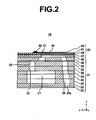
- FIG. 2 is a schematic cross-sectional view which shows a portion of the head 5 enlarged. Note that, the lower part in the sheet in FIG. 2 is the side facing the media 101.
- the head 5 is a piezo type head which applies pressure to the ink by mechanical distortion of the piezoelectric element.
- the head 5 has a plurality of ejection elements 19 for discharging the ink drops.
- FIG. 2 shows one ejection element 19.
- the plurality of ejection elements 19 are for example arranged on an xy plane. Each ejection element 19 corresponds to one dot on the media 101.
- the head 5 has a base 21 (path member) which forms a space for storing ink and a piezoelectric element 23 for applying pressure to the ink stored in the base 21.
- the base 21 and the piezoelectric element 23 are fastened to each other by an ordinary temperature curable adhesive (for example epoxy resin).
- the plurality of ejection elements 19 are configured by bases 21 and piezoelectric elements 23.
- each base 21 a plurality of individual channels 25 (one is shown in FIG. 2 ) and a common channel (reserver) 27 communicated with the plurality of individual channels 25 are formed.
- An individual channel 25 is provided for each ejection element 19, while the common channel 27 is provided common to the plurality of ejection elements 19.
- Each individual channel 25 has a descender (partial flow path) 29 including an ejection hole 29a facing the media 101, a pressurizing chamber 31 communicated with the descender 29, and a supply path 33 for communicating the pressurizing chamber 31 and the common channel 27.
- the plurality of individual channels 25 and the common channel 27 are filled with ink.
- the ink is transmitted from the plurality of pressurizing chambers 31 to the plurality of descenders 29, and a plurality of ink drops are discharged from the plurality of ejection holes 29a. Further, the ink is refilled into the plurality of pressurizing chambers 31 from the common channel 27 through the plurality of supply paths 33.
- each pressurizing chamber 31 is formed to a thickness which is roughly constant in the z-direction and is formed in a roughly diamond shape (see FIG. 3B ) when viewed on a plane.
- One corner of the diamond is communicated with the descender 29, and the corner on the opposite side to that is communicated with the supply path 33.
- a portion of the supply path 33 is made restrictor an area of which in the cross-section perpendicular to the flow direction is smaller than those of the common channel 27 and pressurizing chamber 31.
- the base 21 is configured by for example lamination of a plurality of base plates 35.
- through-holes which configure the plurality of individual channels 25 and common channel 27 are formed.
- the thicknesses and number of laminations of the plurality of base plates 35 may be suitably set in accordance with the shapes etc. of the plurality of individual channels 25 and common channel 27.
- the plurality of base plates 35 may be formed by a suitable material.
- the plurality of base plates 35 are formed by a metal from the viewpoints of workability, strength, etc.
- the metal is, preferably, for example stainless steel from the viewpoint of corrosion resistance.
- FIG. 3A is a cross-sectional view of the vicinity of the piezoelectric element 23 in a direction different from that in FIG. 2
- FIG. 3B is a plan view of the vicinity of the piezoelectric element 23.
- the piezoelectric element 23 shown in FIG. 2 and FIG. 3 is configured by for example a unimorph type piezoelectric element which displaces in a flexure mode.
- the piezoelectric element 23 has a diaphragm 37, a common electrode 39, a piezoelectric body 41, and a plurality of individual electrodes 43 which are laminated in order from the pressurizing chamber 31 side.
- the diaphragm 37, the common electrode 39, and the piezoelectric body 41 are for example provided common to the plurality of pressurizing chambers 31 so as to cover the plurality of pressurizing chambers 31.
- an individual electrode 43 is provided for each pressurizing chamber 31.
- the diaphragm 37 is a plate-shaped member having a constant thickness, is superimposed on the upper surface of the base 21 so as to close the concave pressurizing chambers 31, and is fastened to the base 21.
- the diaphragm 37 is formed by a material having a suitable rigidity (Young's modulus) and is formed by for example a ceramic, silicon oxide, or silicon nitride.
- the common electrode 39 is a layer-shaped electrode having a constant thickness, is superimposed on the diaphragm 37, and is fastened to the diaphragm 37.
- the common electrode 39 is formed by for example silver, platinum, or palladium.
- the piezoelectric body 41 is a plate-shaped member having a constant thickness, is superimposed on the common electrode 39, and is fastened to the common electrode 39.
- the piezoelectric body 41 is formed by for example PZT (lead zirconate titanate) or another ceramic.
- Each individual electrode 43 is a layer-shaped electrode having roughly a constant thickness, is superimposed on the piezoelectric body 41, and is fastened to the piezoelectric body 41.
- the individual electrode 43 includes an individual electrode body 44 which forms roughly the same shape together with the pressurizing chamber 31 (diamond in the present embodiment) when viewed on a plane and is a little bit smaller in width than the pressurizing chamber 31 (expands at the center side of the pressurizing chamber 31) and a leadout electrode 45 which is connected to the corner of that individual electrode body 44.
- the individual electrode 43 is formed by for example silver, platinum, or palladium.
- the base 21 is comprised by a metal, therefore the base 21 has a larger thermal expansion coefficient than the piezoelectric body 41 and consequently has a larger thermal expansion coefficient than the piezoelectric element 23 configured by the piezoelectric body 41 as a principal component.
- the common electrode 39 and individual electrodes 43 have larger thermal expansion coefficients than the piezoelectric body 41.
- the thermal expansion coefficient of the PZT (piezoelectric body 41) is 8 ppm/°C
- the thermal expansion coefficient of the stainless steel (SUS430 prescribed by the Japanese Industrial Standards (JIS) base 21
- the thermal expansion coefficient of an Ag-Pd alloy 70/30 in terms of weight ratio, electrode
- FIG. 3C is a schematic view for explaining a polarization direction of the piezoelectric body 41. Specifically, FIG. 3C schematically shows a representative unit cell (tetragonal crystal 47) of the piezoelectric body 41.
- the piezoelectric body 41 is polarized in the thickness direction (z-direction) as indicated by an arrow labeled as the "c axis". Accordingly, when voltage is applied to the common electrode 39 and an individual electrode 43 and an electric field acts upon the piezoelectric body 41 in the polarization direction, the piezoelectric body 41 contracts in the surface direction (in the xy plane). By this contraction, the diaphragm 37 bends so as to protrude toward the pressurizing chamber 31 side. As a result, the volume of the pressurizing chamber 31 changes, pressure is given to the ink in the pressurizing chamber 31, and printing is carried out. Note that, the orientation of the polarization direction may be either of positive side or negative side in the z-direction. In the following description, the explanation will be given by taking as an example a case where the orientation of the polarization direction is the positive side in the z-direction.
- the piezoelectric body 41 is ideally a single domain crystal given a direction of spontaneous polarization toward one side of the thickness direction (positive side of z-direction) of the piezoelectric body 41. In reality, however, it is a multi-domain crystal. That is, the orientation of polarization direction being the positive side of the z-direction means that a ratio of the domains given the direction of spontaneous polarization toward (roughly) the positive side of x-direction is higher than any of ratios of domains given directions of spontaneous polarization toward the other directions and/or a ratio of the sum of those and/or that the domains given directions of spontaneous polarization toward other directions become directions and ratios where the polarizations are cancelled by each other.
- Each domain is a crystal where the unit cell is regularly arranged in a (roughly) constant orientation.
- the unit cell causes spontaneous polarization in the unit cell by shifting the center of gravity of positive charges and the center of gravity of negative charges in the predetermined plane direction (including equivalent orientation).
- the orientation of polarization direction being the positive side of the z-direction means that the ratio of the unit cells in which the plane direction which becomes the direction of the spontaneous polarization is made to the thickness direction is higher than any of the ratios of the unit cells in which the directions of spontaneous polarization are made other directions and/or the ratio of the sum of those and/or that the unit cells in which the directions of spontaneous polarization are made other directions become directions and ratios where the polarizations are cancelled by each other.
- the unit cell is a tetragonal crystal.
- the longitudinal direction (c-axis, plane direction [002]) is the direction of spontaneous polarization.
- the ratio of the tetragonal crystals 47 which are arranged so that the c-axes are oriented toward (roughly) one side of the thickness direction is relatively high.
- the degree of orientation of the c-axis toward one side of the thickness direction is 44% or more and 56% or less in terms of the Lotgering factor.
- the residual stress in the surface direction is 0 MPa or more and 35 MPa or less.
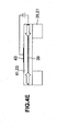
- FIG. 4A to FIG. 4E are cross-sectional views corresponding to FIG. 3A which explain an example of the method of production of the head 5. Note, in order to attach arrows indicating directions of the stress, hatchings on the cross-sections are omitted.
- the base 21 and the piezoelectric element 23 are prepared.
- the manufacturing methods of these parts may be made the same as known general manufacturing methods.
- the base 21 is manufactured by etching or punching a plurality of metal plates to form a plurality of base plates 35 and adhering the plurality of base plates 35 to each other by an adhesive.
- the piezoelectric element 23 is manufactured by preparing green sheets which form the piezoelectric body 41 and diaphragm 37, printing conductive pastes which become the common electrode 39 and individual electrodes 43 on these green sheets (for example the green sheet which becomes the piezoelectric body 41), and laminating and firing these green sheets.
- the thermal expansion coefficients of the common electrode 39 and individual electrodes 43 are higher than the thermal expansion coefficients of the piezoelectric body 41 and diaphragm 37 (ceramic). Accordingly, after these are fastened to each other during firing (in a high temperature state), when the piezoelectric element 23 is made ordinary temperature, the common electrode 39 etc. contract more than the piezoelectric body 41 etc. As a result, as indicated by an arrow y11, in the piezoelectric body 41, compressive stress (residual stress) in the surface direction is generated.
- the piezoelectric element 23 and the base 21 are fastened by the adhesive.
- the fastening is carried out at ordinary temperature by using an ordinary temperature curable adhesive.
- the product may be cooled and compressive stress may be added after that. Further, in such a case, at the working temperature, the degree of orientation of the c-axis toward one side of the thickness direction in the region sandwiched by the electrodes may be 44% or more and 56% or less in terms of the Lotgering factor, and the residual stress in the surface direction may be 0 MPa or more and 35 MPa or less in the compression direction.
- the piezoelectric element 23 and the base 21 are cooled. That is, the temperatures of the piezoelectric element 23 and the base 21 are made temperatures lower than ordinary temperature.
- the cooling may be carried out according to a suitable method.
- these members may be arranged in a cooling chamber or cold air may be sent to these members or a bag in which a heat removing agent is sealed may be brought into contact with these members to perform cooling.
- the base 21 (metal) has a higher thermal expansion coefficient compared with the piezoelectric element 23 containing a ceramic as the principal component. Accordingly, as indicated by an arrow y13, the base 21 tries to contract more than the piezoelectric element 23. As a result, as indicated by an arrow y15 which is made larger than the arrow y11 in FIG. 4A and FIG. 4B , the compressive stress of the piezoelectric body 41 becomes larger.
- the tetragonal crystals 47 change the orientation of the c-axes to a direction perpendicular to the compression direction by 90° by the compressive stress (90° domain switching occurs). Due to this, the degree of orientation of the c-axis toward the thickness direction (up-down direction on the drawing sheet) becomes higher.
- the cooling of the piezoelectric element 23 and base 21 is ended (the piezoelectric element 23 and base 21 are made the ordinary temperature).
- the piezoelectric element 23 and base 21 are made ordinary temperature in the same way as the time of bonding. Therefore, as indicated by the arrow y11 the same as the arrow y11 in FIG. 4B , the compressive stress of the piezoelectric body 41 returns to the magnitude before cooling (even when the stress does not return to a completely original state due to occurrence of domain switching, the difference is small relative to the stress generated due to the temperature change).
- the piezoelectric body 41 is processed to polarize it. Specifically, a DC voltage is applied between the common electrode 39 and an individual electrode 43 by a DC power supply 51. The voltage at this time is made a voltage which forms an electric field having a strength exceeding a coercive electric field of the piezoelectric body 41. More suitably, this is made a voltage not less than the voltage by which the polarization becomes saturated.
- the polarization treatment is for example carried out at ordinary temperature. Further, the order of steps of the bonding and polarization treatment may be reverse as well. However, when the thickness of the piezoelectric element 23 is a thin one of about 100 ⁇ m or less, warping occurs in the piezoelectric element 23 due to the polarization treatment, therefore the bonding becomes difficult. Therefore, the order of steps explained above is preferable. Further, the compressive stress which is added to the piezoelectric body 41 is influenced by the structure of the head 5.
- the tetragonal crystals 47 (domain) of the piezoelectric body 41 orient the directions of c-axes toward a direction in which the electric field is applied (one side of the thickness direction, positive side of the z-direction) by application of the electric field. That is, the piezoelectric body 41 is polarized while defining one side of the thickness direction as the polarization direction. After that, even after the application of the electric field is suspended, some of the tetragonal crystals 47 remain orienting c-axes toward one side of the thickness direction. That is, the polarization remains.
- the degree of orientation of the c-axis toward the thickness direction is raised in advance by the cooling treatment ( FIG. 4C ), it becomes higher compared with the case where the cooling treatment is not carried out. Note that, even in a case where the cooling treatment is carried out after the polarization treatment, in the same way, compared with the case where the cooling treatment is not carried out, the degree of orientation of the c-axis toward the thickness direction becomes higher.
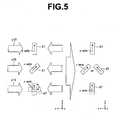
- FIG. 5 is a conceptual view for explaining the domain switching in the cooling treatment in FIG. 4C .
- the orientations of the c-axes of the plurality of domains are random. Note that, on the left side in FIG. 5 , a tetragonal crystal 47 c-axis of which is oriented toward the positive side of the z-direction, a tetragonal crystal 47 c-axis of which is oriented inclined with an angle of 45° relative to the z-direction, and a tetragonal crystal 47 c-axis of which is oriented toward the direction perpendicular to the z-direction are exemplified.
- the domain c-axis of which was oriented toward the z-direction from the time before the cooling treatment does not change the orientation of the c-axis.
- the domain c-axis of which was oriented toward the direction perpendicular to the z-direction before the cooling treatment orients the c-axis toward the z-direction due to the occurrence of the 90° domain switching.
- the domain c-axis of which was oriented inclined by 45° relative to the z-direction before the cooling treatment orients the c-axis inclined by 45° relative to the z-direction even if 90° domain switching occurs.
- the piezoelectric body 41 includes a domain which contributes to an increase of the degree of orientation of the c-axis toward the z-direction due to the 90° domain switching and a domain which does not contribute to the above increase.
- the piezoelectric material for the purpose of an actuator, a material which is generally called as a soft material and has a composition in the vicinity of the morphotropic phase boundary (MPB) is selected.
- MPB morphotropic phase boundary
- the degree of orientation can be made higher than the range described above. Note, the application of such an orientation technique causes an increase of cost.
- the piezoelectric element 23 including the piezoelectric body 41 and the base having a higher thermal expansion coefficient than the piezoelectric element 23 are fastened, then they are cooled down to a temperature lower than ordinary temperature. Due to this, compressive stress is given to the piezoelectric body 41 and the degree of orientation of the c-axis toward the z-direction is made high. That degree of orientation is maintained even when the cooling treatment is ended.
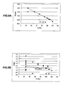
- FIG. 6A and FIG. 6B are graphs which show evidence that the degree of orientation changes due to the compressive stress, and the degree of orientation is maintained even when the compressive stress is removed after that.
- FIG. 6A and FIG. 6B show examples of results of XRD (X-ray diffraction (method)) with respect to the major surface of the piezoelectric body 41.
- X-rays are applied to the major surface of the piezoelectric body 41, and the intensity I of the reflected X-rays is measured.
- the irradiation angle ⁇ (°) of the X-rays with respect to the major surface in a side view of the major surface is changed.
- the abscissas show 2 ⁇ (°)
- ordinates show the intensities I.
- a line L1 indicates the XRD results before bonding of the piezoelectric element 23 to the base 21, and a line L2 indicates the XRD results after bonding of the piezoelectric element 23 to the base 21.
- the piezoelectric element 23 and the base 21 were bonded by using a thermosetting resin at a temperature of 125°C unlike the present embodiment, while the XRD was measured at ordinary temperature. Accordingly, after bonding, when the temperature falls to one within the range of the ordinary temperature, by contraction of the base 21 more than the piezoelectric element 23, compressive stress is generated in the piezoelectric body 41.
- the line L1 indicates the degree of orientation before compressive stress is generated
- the line L2 indicates the degree of orientation after compressive stress is generated.
- a line L3 indicates the XRD results in a state where the piezoelectric element 23 and the base 21 are adhered
- a line L4 indicates the XRD results after the piezoelectric element 23 is peeled off from the base 21. That is, the line L3 indicates the degree of orientation in a state where compressive stress is generated, and the line L4 indicates the degree of orientation in a state where that compressive stress is removed.
- the line L3 in FIG. 6B in the same way as FIG. 6A , also indicates the results when the piezoelectric element 23 and the base 21 were adhered at a high temperature by using a thermosetting resin and the XRD was measured at ordinary temperature, but the conditions are different from FIG. 6A , so this does not coincide with the line L2.
- the piezoelectric element 23 was peeled off (correctly speaking, the piezoelectric body 41 was peeled off at the common electrode 39 section) by dipping the piezoelectric element 23 and the base 21 in an aqueous solution of 1 mol/NaCl and applying DC voltage (voltage within the withstand voltage) to the common electrode 39 and individual electrode 43 by a W probe so that no load was applied to the piezoelectric body 41 from the outside in the peeling process.
- the intensity I at 2 ⁇ corresponding to the (200) plane and (002) plane does not greatly change. That is, the degree of orientation which changed due to the compressive stress is maintained even when the compressive stress is removed.
- the degree of orientation of the c-axis toward the z-direction is made high.
- variation in displacement is suppressed.
- they are adhered at ordinary temperature, therefore application of compressive stress from the base 21 to the piezoelectric element 23 at the ordinary temperature is suppressed, so a drop of displacement is suppressed.
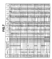
- FIG. 7 and FIG. 14 are tables which show the conditions and modes of operation etc. of the examples and comparative examples.
- the columns of "No.” indicate numbers which are suitably attached to the examples and comparative examples.
- 40 samples ones obtained by bonding the piezoelectric element 23 and base 21
- various measurements were carried out. Note that, in “No. 1", as the sample, use is made of a piezoelectric body 41 before it was adhered to the base 21, and some of the conditions or modes of operation are not described.
- the column of "Zr/Ti" indicates the conditions of the material of the piezoelectric body 41.
- the material of the piezoelectric body 41 was made, among ones represented by Pb 1-x-y Sr x Ba y (Zn 1/3 Sb 2/3 ) a (Ni 1/2 Te 1/2 ) b Zr 1-a-b-c Ti c O 3 + ⁇ wt%Pb 1/2 NbO 3 (0 ⁇ x ⁇ 0.14, 0 ⁇ y ⁇ 0.14, 0.05 ⁇ a ⁇ 0.1, 0.002 ⁇ b ⁇ 0.01, 0.44 ⁇ c ⁇ 0.50, ⁇ is 0.1 or more and 1.0 or less), a material in which (1-a-b-c)/c becomes 0.5/0.5 or 0.495/0.505.
- values of (1-a-b-c)/c are shown in the columns of "Zr/Ti”.
- T1(°C) indicate the conditions of the temperature of the atmosphere (consequently the temperatures of the piezoelectric element 23 and base 21) when the piezoelectric element 23 and the base 21 were adhered. As indicated in these columns, various bonding temperatures T1 were set within a range of 25 to 120°C.
- T2(°C) indicate the conditions of the minimum temperature of the piezoelectric element 23 and the base 21 after bonding. Note that, in the examples, the conditions of temperature at the time of the cooling treatment ( FIG. 4C ) are shown. As indicated in these columns, various minimum temperatures T2 are set within a range of -70 to 0°C which is lower than ordinary temperature (5°C or more and 35°C or less) in the examples, while are set within the range of ordinary temperature (mainly 25°C) in the comparative examples.
- ⁇ T(°C) The columns of " ⁇ T(°C)" indicate differences between the bonding temperatures T1 and the minimum temperatures T2 (T2-T1). As shown in these columns, various temperature differences ⁇ T are set at 0 to 180°C.
- the columns of " ⁇ (MPa)" indicate the measurement results of the compressive stress which is generated in the piezoelectric body 41.
- the compressive stress was measured according to the full Debye ring fitting 2D process. This measures the XRD in a state where stress is applied to a sample having the same composition as the target and measures the XRD of the sample as the target to thereby measure the compressive stress based on distortion of the crystal cell due to stress. Note that, the numerical values in the columns are given minus marks corresponding to stress being applied in the compression direction.
- the columns of "(002)/ ⁇ (200)+(002) ⁇ " indicate the values obtained by dividing the intensity I of the (002) plane measured according to XRD in the same way as FIG. 6 by the intensity I of the (200) plane and (002) plane (one type of index showing the degree of orientation).
- the columns of "LF(%)" indicate the degrees of orientation of the c-axis toward one side of the thickness direction in the piezoelectric body 41. Specifically, these columns indicate the Lotgering factors calculated based on the intensities I measured according to XRD.
- the columns of "D(nm)" indicate displacements at the center position of the piezoelectric element 23 when voltage is applied to between the common electrode 39 and an individual electrode 43 and the piezoelectric element 23 is bent.
- the columns of "V(%)" indicate the variations of the displacement D described above among a plurality of ejection elements 19. Specifically, the displacement variation V indicates the standard deviation D ⁇ of the displacement D.
- the polarization treatment is carried out by applying voltage between the common electrode 39 and an individual electrode 43 as explained in the embodiments.
- the polarization treatment was carried out by forming a temporary electrode for polarization on the major surface of the piezoelectric body 41 and applying voltage between that temporary electrode and the common electrode 39. Accordingly, the piezoelectric body 41 was polarized in the thickness direction over its entire surface. Note that, the temporary electrode was removed after the polarization treatment.
- the polarization treatment was carried out by forming a temporary electrode for polarization on the periphery of an individual electrode 43, applying voltage between the common electrode 39 and the individual electrode 43, and applying voltage between the individual electrode 43 and the temporary electrode. Accordingly, the piezoelectric body 41 was polarized in the surface direction on the periphery of the individual electrode 43. Note that, the temporary electrode was removed after the polarization treatment.
- the conditions of the production method differ only in the bonding temperature T1, the minimum temperature T2, and the temperature difference ⁇ T.
- the displacements D and the displacement variations V are different from each other. That is, the bonding temperature T1, the minimum temperature T2, and the temperature difference ⁇ T exert influences upon the displacements D and the displacement variations V.
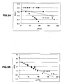
- FIG. 8A is a graph which shows correlation between the bonding temperature T1 and the displacement D in which the abscissa shows the bonding temperature T1, and the ordinate shows the displacement D.
- FIG. 8B is a graph which shows correlation between the bonding temperature T1 and the displacement variation V in which the abscissa shows the bonding temperature T1, and the ordinate shows the displacement variations V.
- FIG. 9A is a graph which shows correlation between the temperature difference ⁇ T and the displacement D in which the abscissa shows the temperature difference ⁇ T, and the ordinate shows the displacement D.
- FIG. 9B is a graph which shows correlation between the temperature difference ⁇ T and the displacement variation V in which the abscissa shows the temperature difference ⁇ T, and the ordinate shows the displacement variation V.
- the displacement D largely depends upon the bonding temperature T1.
- the bonding temperature T1 when the bonding temperature T1 is high, at ordinary temperature, compressive stress is generated in the piezoelectric body 41 due to the contraction of the base 21, so the piezoelectric constant of the piezoelectric body 41 becomes low.
- the displacement variation V largely depends upon the temperature difference ⁇ T. The reason for this is considered that, if the temperature difference ⁇ T is large, as explained with reference to FIG. 4C , compressive stress in the surface direction is generated in the piezoelectric body 41, therefore the degree of orientation of the c-axis toward the thickness direction becomes high.
- correlation diagrams for confirming these modes of operation will be shown.
- FIG. 10A is a graph which shows correlation between the bonding temperature T1 and the compressive stress ⁇ in which the abscissa shows the bonding temperature T1, and the ordinate shows the compressive stress ⁇ .
- FIG. 10B is a graph which shows correlation between the bonding temperature T1 and an orientation degree LF of the c-axis toward the thickness direction in which the abscissa shows the bonding temperature T1, and the ordinate shows the orientation degree LF.
- FIG. 11A is a graph which shows correlation between the temperature difference ⁇ T and the compressive stress ⁇ in which the abscissa shows the temperature difference ⁇ T, and the ordinate shows the compressive stress ⁇ .
- FIG. 11B is a graph which shows correlation between the temperature difference ⁇ T and the orientation degree LF of the c-axis toward the thickness direction in which the abscissa shows the temperature difference ⁇ T, and the ordinate shows the orientation degree LF.
- FIG. 12A is a graph which shows correlation between the compressive stress ⁇ and the displacement D in which the abscissa shows the compressive stress ⁇ , and the ordinate shows the displacement D.
- FIG. 12B is a graph which shows correlation between the compressive stress ⁇ and the displacement variation V in which the abscissa shows the compressive stress ⁇ , and the ordinate shows the displacement variation V.
- FIG. 13A is a graph which shows correlation between the orientation degree LF of the c-axis toward the thickness direction and the displacement D in which the abscissa shows the orientation degree LF, and the ordinate shows the displacement D.
- FIG. 13B is a graph which shows correlation between the orientation degree LF and the displacement variation V in which the abscissa shows the orientation degree LF, and the ordinate shows the displacement variation V.
- the displacement variation V can be made small while securing a large displacement D.
- the displacement variation V can be made small while securing a large displacement D.
- a preferred range of that is as follows.
- the displacement variation V of that is 4.1%.
- the displacement variation V is 3.0%.
- the displacement variation V is 2.8%.
- the displacement variations V in both of No. 17 and No. 18 are smaller than the displacement variation V in No. 2.
- the temperature difference ⁇ T is made 65°C or more (if bonding at ordinary temperature, it is cooled up to -40°C or less).
- the bonding is preferably carried out at ordinary temperature and a temperature close to ordinary temperature (for example 50°C or less. See No. 26). More preferably, the bonding is carried out at a temperature within a range of ordinary temperature.
- the orientation degrees LF of the c-axis toward the thickness direction in the piezoelectric body 41 is 44% (see No. 21) or more and 56% (see No. 26) or less, and the compressive stresses ⁇ in the surface direction of the piezoelectric body 41 are 0 MPa or more and 35 MPa (see No. 26) or less.
- the combination of the piezoelectric element 23 and the base 21 is one example of the piezoelectric actuator.
- the present invention is not limited to the above embodiments and may be executed in various ways.
- the piezoelectric actuator is not limited to one used in an ink jet head and may be one used for various applications. Further, the piezoelectric element is not limited to a unimorph type and may for example be a bimorph type as well. For the deformation mode of piezoelectric as well, d 33 other than d 31 or one using a shear mode may be employed.
- the piezoelectric actuator can be used for other than an ink jet head, for example, a piezoelectric speaker, a source of vibration for transmitting the sense of touch in a display device equipped with a touch sensor or the like, and a source of vibration for transmitting audio information by making the display device such as a mobile phone contact an ear or other portion of the human body and giving vibration and so on.
- the piezoelectric element is superimposed in the thickness direction with respect to the flat plate-shaped base and fastened.
- the base is a film made of resin such as polyethylene, polyimide or polypropylene or metal. Basically use is made of one having a larger thermal expansion coefficient than a piezoelectric element.
- the film may be spread in a frame that becomes the fastening end of vibration of the film.
- the piezoelectric element is basically fastened at the center part of the film so that the vibration of the film can be made larger. It is also possible to make a portion of the display device vibrate and act as the piezoelectric speaker. An explanation of this will be given next together with the other forms.
- the transmission of the sense of touch in the display device equipped with a touch sensor means for example transmitting the fact of detection of depression when a finger etc. pushes a liquid crystal touch panel etc., by vibration etc. to the finger.
- a feeling can be generated like if a button were pushed.
- vibration is given to outer ears etc. so that it is perceived by the inner ears as sound. This can be used in place of sound transmitted by vibration of air or can be used to assist sound which is transmitted by vibration of air. In any case, it can be realized by fastening the piezoelectric element on a base which is a part of a display device such as a liquid crystal panel and making this vibrate.
- the base is glass or acrylic resin. They basically have a larger thermal expansion coefficient than a piezoelectric element.
- the glass to be used there are ones having low thermal expansion coefficients.
- a member having a high thermal expansion coefficient such as a metal plate may be inserted between the glass and the piezoelectric element so that a compressive stress is applied to the piezoelectric element.
- the base for example, use can be made of one having a thickness of 0.1 mm or more and 2.0 mm or less and a size of a few centimeters to several tens of centimeters.
- the center part is used for realizing other functions in many cases, therefore a piezoelectric element is basically fastened near an end part of the base.
- the size of the piezoelectric element for example, use can be made of one having a thickness of 0.1 or more and 1.0 mm or less, a length of 10mm or more and 50 mm or less, and a width of 1.0mm or more and 10.0 mm or less.
- the size in one of directions along the base is preferably larger than the thickness (height from the base) so that the stress from the base is easily added to the entire piezoelectric element. Further, preferably the sizes in the all directions along the base are larger than the thickness.
- the material of the piezoelectric body is not limited to PZT and has only to be a material with which a 90° domain switch occurs due to compressive stress.
- it may be a material containing a tetragonal principal crystal phase.
- the material of the piezoelectric body is one represented by Pb 1-x-y Sr x Ba y (Zn 1/3 Sb 2/3 )a(Ni 1/2 Te 1/2 ) b Zr 1-a-b-c Ti c O 3 + ⁇ wt%Pb 1/2 NbO 3 (0 ⁇ x ⁇ 0.14, 0 ⁇ y ⁇ 0.14, 0.05 ⁇ a ⁇ 0.1, 0.002 ⁇ b ⁇ 0.01, 0.44 ⁇ c ⁇ 0.50, ⁇ is 0.1 or more and 1.0 or less), (1-a-b-c)/c may be suitably set. For example, it may be a value between 0.5/0.5 and 0.49/0.505 shown in the examples as well.
- the piezoelectric body need only satisfy the conditions of the degree of orientation or compressive stress in at least a region sandwiched by a pair of electrodes (common electrode and individual electrode).
- the piezoelectric body may be polarized in the surface direction, may be polarized in the thickness direction or may not be polarized.
Landscapes
- Engineering & Computer Science (AREA)
- Chemical & Material Sciences (AREA)
- Ceramic Engineering (AREA)
- Manufacturing & Machinery (AREA)
- Composite Materials (AREA)
- Materials Engineering (AREA)
- Structural Engineering (AREA)
- Organic Chemistry (AREA)
- Particle Formation And Scattering Control In Inkjet Printers (AREA)
Abstract
Description
- The present invention relates to a piezoelectric actuator, an ink jet head, and a method for producing a piezoelectric actuator.
- There are known a piezoelectric actuator which utilizes deformation of a piezoelectric element and a piezo type ink jet head which applies pressure to ink by a piezoelectric actuator to discharge ink drops (for example
P Patent Literature 1 and 2). - For example, the piezoelectric actuator of an ink jet head in
Patent Literature 1 has a base in which a plurality of concave pressurizing chambers in which ink is filled are formed and a piezoelectric element which is superimposed on and fastened to the base so as to close the pressurizing chambers. The piezoelectric element inPatent Literature 1 is a so-called unimorph type and has, from the base side, a diaphragm, common electrode, piezoelectric body, and individual electrodes in that order. The piezoelectric body is polarized in a thickness direction (lamination direction). When voltage is applied to the piezoelectric body by the common electrode and individual electrodes, the piezoelectric body contracts in the surface direction and that contraction is limited by the diaphragm. As a result, the piezoelectric element is bent to the pressurizing chamber side (center side displaces to the pressurizing chamber side), so pressure is given to the ink in the pressurizing chamber. -
- Patent Literature 1: Japanese Patent Publication No.
2006-174618A - Patent Literature 2: Japanese Patent Publication No.
2010-228145A - The piezoelectric element and the base are for example bonded by using a thermosetting resin in a high temperature state. On the other hand, the base is for example comprised of a metal from the viewpoints of strength and workability, therefore is higher in thermal expansion coefficient compared with the piezoelectric body. Accordingly, when the piezoelectric actuator is brought to an ordinary temperature after bonding, the base contracts more than the piezoelectric body, therefore a residual stress in the surface direction is generated in the piezoelectric body. As a result, the piezoelectric body exhibits a state where it is contracted in the surface direction even in a state where a voltage is not applied, therefore the displacement of the piezoelectric element when a voltage is applied is lowered.
- Therefore, bonding the piezoelectric elements and the base material at an ordinary temperature may be considered. In this case, however, variations of displacement arise among the plurality of pressurizing chambers or among the plurality of piezoelectric actuators (plurality of ink jet heads).
- Accordingly, desirably a piezoelectric actuator, an ink jet head, and a method for producing the piezoelectric actuator which are capable of suppressing variations in displacement are provided.
- A piezoelectric actuator according to one aspect of the present invention has a base; and a piezoelectric element which has a plate-shaped piezoelectric body and a pair of electrodes arranged so as to sandwich the piezoelectric body in a thickness direction and is superimposed on and fastened to the base in the thickness direction. The base has a higher thermal expansion coefficient than the piezoelectric element. and the piezoelectric body has a tetragonal principal crystal phase, in which the degree of orientation of the c-axis toward one side in the thickness direction in the region sandwiched by the pair of electrodes is 44% or more and 56% or less in terms of the Lotgering factor and in which the residual stress in the surface direction is 0MPa or more and 35 MPa or less in the direction of compression.
- An ink jet head according to one aspect of the present invention has a base provided with a concave pressurizing chamber for holding ink; and a piezoelectric element which has a plate-shaped piezoelectric body and a pair of electrodes arranged so as to sandwich the piezoelectric body in a thickness direction and is superimposed on and fastened to the base in the thickness direction so as to close the pressurizing chamber. The base has a higher thermal expansion coefficient than the piezoelectric element. The piezoelectric body has a tetragonal principal crystal phase, in which the degree of orientation of the c-axis toward one side in the thickness direction in the region sandwiched by the pair of electrodes is 44% or more and 56% or less in terms of the Lotgering factor, and the residual stress in the surface direction is 0 MPa or more and 35 MPa or less in the direction of compression.
- A method for producing a piezoelectric actuator according to one aspect of the present invention includes a step of preparing a piezoelectric element which has a plate-shaped piezoelectric body and a pair of electrodes arranged so as to sandwich the piezoelectric body in the thickness direction; a step of preparing a base having a higher thermal expansion coefficient than the piezoelectric element; a step of superimposing the piezoelectric element and the base on each other in the thickness direction and fastening them; and a step of, after the step of fastening, cooling the piezoelectric element and the base down to a temperature lower than ordinary temperature.
- According to the above configurations or procedures, variations in displacement can be suppressed.
-
- [
FIG. 1 ] A perspective view which schematically shows principal parts of a recording apparatus according to an embodiment of the present invention. - [
FIG. 2 ] A cross-sectional view of a portion of an ink jet head of the recording apparatus inFIG. 1 . - [
FIGS. 3] FIG. 3A and FIG. 3B are a cross-sectional view and a plan view which show an actuator of the head inFIG. 2 , andFIG. 3C is a schematic view for explaining a polarization direction of a piezoelectric body of the actuator. - [
FIGS. 4] FIG. 4A to FIG. 4E are cross-sectional views for explaining an example of a method of production of a head. - [
FIG. 5 ] A conceptual view for explaining domain switching in a cooling treatment inFIG. 4C . - [
FIGS. 6] FIG. 6A and FIG. 6B are graphs for explaining a change of a degree of orientation and fastening according to a compressive stress. - [
FIG. 7 ] A table which shows conditions and modes of operation etc. of examples and comparative examples. - [
FIGS. 8] FIG. 8A is a graph which shows correlation between a bonding temperature and displacement, andFIG. 8B is a graph which shows correlation between the bonding temperature and variation in displacement. - [
FIGS. 9] FIG. 9A is a graph which shows correlation between a temperature difference and displacement, andFIG. 9B is a graph which shows correlation between the temperature difference and variation in displacement. - [
FIGS. 10] FIG. 10A is a graph which shows correlation between the bonding temperature and compressive stress, andFIG. 10B is a graph which shows correlation between the bonding temperature and a degree of orientation. - [
FIGS. 11] FIG. 11A is a graph which shows correlation between the temperature difference and compressive stress, andFIG. 11B is a graph which shows correlation between the temperature difference and the degree of orientation. - [
FIGS. 12] FIG. 12A is a graph which shows correlation between compressive stress and displacement, andFIG. 12B is a graph which shows correlation between the compressive stress and variation in displacement. - [
FIGS. 13] FIG. 13A is a graph which shows correlation between the degree of orientation and displacement, andFIG. 13B is a graph which shows a correlation between the degree of orientation and variation in displacement. - [
FIG. 14 ] A table which shows the conditions and modes of operation etc. of examples and comparative examples in addition toFIG. 7 . -
FIG. 1 is a perspective view which schematically shows principal parts of arecording apparatus 1 according to an embodiment of the present invention. - Note that, in the
recording apparatus 1 and anink jet head 5 which will be explained later, any direction may be made upward or downward. However, in the following description, for convenience, an orthogonal coordinate system xyz is defined, and use is sometimes made of an "upper surface", "lower surface", and other terms where the positive side of the z-direction (upper part in the drawing sheet inFIG. 1 ) is the upper part. - The
recording apparatus 1 has forexample conveyance parts 3 which carry a media (for example paper) 101 to a direction indicated by an arrow y1, ahead 5 which discharges ink drops toward themedia 101 which is being conveyed, and acontrol part 7 which controls operations of theconveyance parts 3 and thehead 5. - The
conveyance parts 3 for example convey a plurality ofmedia 101 stacked in a not shown supply stack one by one to a not shown discharge stack. Theconveyance parts 3 may be given a known suitable configuration.FIG. 1 exemplifies conveyance parts which have a conveyance route made a straight path and are provided withrollers 9 abutting against themedia 101 andmotors 11 for rotating therollers 9. - The
head 5 is arranged in the middle of the conveyance route of themedia 101 and faces themedia 101 from the positive side of the z-direction. Thehead 5 may be a serial head which performs a shuttle movement in the direction (main scanning direction, x-direction) perpendicular to the printing surface and conveyance direction of themedia 101 or may be a line head which is (substantially) fastened in the perpendicular direction. Note that, in the present embodiment, an explanation will be given by taking as an example a case where thehead 5 is a line head. - The
head 5 ejects and deposits ink drops upon themedia 101 at a plurality of positions in the x-direction. By repeatedly performing the operation along with the conveyance of themedia 101, a two-dimensional image is formed on themedia 101. - The
control part 7 is configured by including for example a CPU, ROM, RAM, and external memory unit. Thecontrol part 7 outputs control signals to motor-use drivers 13 to thereby apply desired voltages to themotors 11 to control themotors 11. In the same way, thecontrol part 7 outputs control signals to a head-use driver 15 to thereby apply a desired voltage to thehead 5 to control thehead 5. - The head-
use driver 15, or the head-use driver 15 and a portion ofcontrol part 7 configures a drivesignal output part 8 which generates a drive signal (voltage to be applied to the head 5) containing a drive pulse (drive waveform) having a predetermined drive frequency and outputs the same to thehead 5. The drivesignal output part 8 is configured by for example a driver IC or circuit board. - Note that, in
FIG. 1 , the drivesignal output part 8 and thehead 5 are shown as parts which are different from each other. However, a portion or all of the drivesignal output part 8 may be mounted on thehead 5 as well. In this case, it is also possible to grasp thehead 5 and the section (a portion or all) of the drivesignal output part 8 which is mounted on thehead 5 as configuring ahead 6 in a broad sense as a whole. -
FIG. 2 is a schematic cross-sectional view which shows a portion of thehead 5 enlarged. Note that, the lower part in the sheet inFIG. 2 is the side facing themedia 101. - The
head 5 is a piezo type head which applies pressure to the ink by mechanical distortion of the piezoelectric element. Thehead 5 has a plurality ofejection elements 19 for discharging the ink drops.FIG. 2 shows oneejection element 19. The plurality ofejection elements 19 are for example arranged on an xy plane. Eachejection element 19 corresponds to one dot on themedia 101. - Further, from another viewpoint, the
head 5 has a base 21 (path member) which forms a space for storing ink and apiezoelectric element 23 for applying pressure to the ink stored in thebase 21. Although particularly not shown, thebase 21 and thepiezoelectric element 23 are fastened to each other by an ordinary temperature curable adhesive (for example epoxy resin). The plurality ofejection elements 19 are configured bybases 21 andpiezoelectric elements 23. - Inside each base 21, a plurality of individual channels 25 (one is shown in
FIG. 2 ) and a common channel (reserver) 27 communicated with the plurality ofindividual channels 25 are formed. Anindividual channel 25 is provided for eachejection element 19, while thecommon channel 27 is provided common to the plurality ofejection elements 19. - Each
individual channel 25 has a descender (partial flow path) 29 including anejection hole 29a facing themedia 101, a pressurizingchamber 31 communicated with thedescender 29, and asupply path 33 for communicating the pressurizingchamber 31 and thecommon channel 27. - The plurality of
individual channels 25 and thecommon channel 27 are filled with ink. By the volume of the plurality of pressurizingchamber 31 changing and pressure being given to the ink, the ink is transmitted from the plurality of pressurizingchambers 31 to the plurality ofdescenders 29, and a plurality of ink drops are discharged from the plurality ofejection holes 29a. Further, the ink is refilled into the plurality of pressurizingchambers 31 from thecommon channel 27 through the plurality ofsupply paths 33. - The cross-sectional shapes or planar shapes of the plurality of
individual channels 25 and thecommon channel 27 may be suitably set. In the present embodiment, each pressurizingchamber 31 is formed to a thickness which is roughly constant in the z-direction and is formed in a roughly diamond shape (seeFIG. 3B ) when viewed on a plane. One corner of the diamond is communicated with thedescender 29, and the corner on the opposite side to that is communicated with thesupply path 33. A portion of thesupply path 33 is made restrictor an area of which in the cross-section perpendicular to the flow direction is smaller than those of thecommon channel 27 and pressurizingchamber 31. - The
base 21 is configured by for example lamination of a plurality ofbase plates 35. In thebase plates 35, through-holes which configure the plurality ofindividual channels 25 andcommon channel 27 are formed. The thicknesses and number of laminations of the plurality ofbase plates 35 may be suitably set in accordance with the shapes etc. of the plurality ofindividual channels 25 andcommon channel 27. - The plurality of
base plates 35 may be formed by a suitable material. For example, the plurality ofbase plates 35 are formed by a metal from the viewpoints of workability, strength, etc. The metal is, preferably, for example stainless steel from the viewpoint of corrosion resistance. -
FIG. 3A is a cross-sectional view of the vicinity of thepiezoelectric element 23 in a direction different from that inFIG. 2 , andFIG. 3B is a plan view of the vicinity of thepiezoelectric element 23. - The
piezoelectric element 23 shown inFIG. 2 andFIG. 3 is configured by for example a unimorph type piezoelectric element which displaces in a flexure mode. Specifically, for example, thepiezoelectric element 23 has adiaphragm 37, acommon electrode 39, apiezoelectric body 41, and a plurality ofindividual electrodes 43 which are laminated in order from the pressurizingchamber 31 side. - The
diaphragm 37, thecommon electrode 39, and thepiezoelectric body 41 are for example provided common to the plurality of pressurizingchambers 31 so as to cover the plurality of pressurizingchambers 31. On the other hand, anindividual electrode 43 is provided for each pressurizingchamber 31. - The
diaphragm 37 is a plate-shaped member having a constant thickness, is superimposed on the upper surface of the base 21 so as to close theconcave pressurizing chambers 31, and is fastened to thebase 21. Thediaphragm 37 is formed by a material having a suitable rigidity (Young's modulus) and is formed by for example a ceramic, silicon oxide, or silicon nitride. - The
common electrode 39 is a layer-shaped electrode having a constant thickness, is superimposed on thediaphragm 37, and is fastened to thediaphragm 37. Thecommon electrode 39 is formed by for example silver, platinum, or palladium. - The
piezoelectric body 41 is a plate-shaped member having a constant thickness, is superimposed on thecommon electrode 39, and is fastened to thecommon electrode 39. Thepiezoelectric body 41 is formed by for example PZT (lead zirconate titanate) or another ceramic. - Each
individual electrode 43 is a layer-shaped electrode having roughly a constant thickness, is superimposed on thepiezoelectric body 41, and is fastened to thepiezoelectric body 41. Theindividual electrode 43 includes anindividual electrode body 44 which forms roughly the same shape together with the pressurizing chamber 31 (diamond in the present embodiment) when viewed on a plane and is a little bit smaller in width than the pressurizing chamber 31 (expands at the center side of the pressurizing chamber 31) and aleadout electrode 45 which is connected to the corner of thatindividual electrode body 44. Theindividual electrode 43 is formed by for example silver, platinum, or palladium. - Note that, as explained above, the
base 21 is comprised by a metal, therefore thebase 21 has a larger thermal expansion coefficient than thepiezoelectric body 41 and consequently has a larger thermal expansion coefficient than thepiezoelectric element 23 configured by thepiezoelectric body 41 as a principal component. Further, thecommon electrode 39 andindividual electrodes 43 have larger thermal expansion coefficients than thepiezoelectric body 41. For example, the thermal expansion coefficient of the PZT (piezoelectric body 41) is 8 ppm/°C, the thermal expansion coefficient of the stainless steel (SUS430 prescribed by the Japanese Industrial Standards (JIS), base 21) is 10 ppm/°C, and the thermal expansion coefficient of an Ag-Pd alloy (70/30 in terms of weight ratio, electrode) is 17 ppm/°C. -
FIG. 3C is a schematic view for explaining a polarization direction of thepiezoelectric body 41. Specifically,FIG. 3C schematically shows a representative unit cell (tetragonal crystal 47) of thepiezoelectric body 41. - The
piezoelectric body 41 is polarized in the thickness direction (z-direction) as indicated by an arrow labeled as the "c axis". Accordingly, when voltage is applied to thecommon electrode 39 and anindividual electrode 43 and an electric field acts upon thepiezoelectric body 41 in the polarization direction, thepiezoelectric body 41 contracts in the surface direction (in the xy plane). By this contraction, thediaphragm 37 bends so as to protrude toward the pressurizingchamber 31 side. As a result, the volume of the pressurizingchamber 31 changes, pressure is given to the ink in the pressurizingchamber 31, and printing is carried out. Note that, the orientation of the polarization direction may be either of positive side or negative side in the z-direction. In the following description, the explanation will be given by taking as an example a case where the orientation of the polarization direction is the positive side in the z-direction. - Here, the
piezoelectric body 41 is ideally a single domain crystal given a direction of spontaneous polarization toward one side of the thickness direction (positive side of z-direction) of thepiezoelectric body 41. In reality, however, it is a multi-domain crystal. That is, the orientation of polarization direction being the positive side of the z-direction means that a ratio of the domains given the direction of spontaneous polarization toward (roughly) the positive side of x-direction is higher than any of ratios of domains given directions of spontaneous polarization toward the other directions and/or a ratio of the sum of those and/or that the domains given directions of spontaneous polarization toward other directions become directions and ratios where the polarizations are cancelled by each other. - Each domain is a crystal where the unit cell is regularly arranged in a (roughly) constant orientation. The unit cell causes spontaneous polarization in the unit cell by shifting the center of gravity of positive charges and the center of gravity of negative charges in the predetermined plane direction (including equivalent orientation). Accordingly, from a viewpoint different from that described above, the orientation of polarization direction being the positive side of the z-direction means that the ratio of the unit cells in which the plane direction which becomes the direction of the spontaneous polarization is made to the thickness direction is higher than any of the ratios of the unit cells in which the directions of spontaneous polarization are made other directions and/or the ratio of the sum of those and/or that the unit cells in which the directions of spontaneous polarization are made other directions become directions and ratios where the polarizations are cancelled by each other.
- For example, when the
piezoelectric body 41 is PZT wherein x of ZrxTix-1 is less than 0.525 (the boundary of numerical values changes a little according to other additives), the unit cell is a tetragonal crystal. In a tetragonal crystal, the longitudinal direction (c-axis, plane direction [002]) is the direction of spontaneous polarization. Further, in thepiezoelectric body 41, the ratio of thetetragonal crystals 47 which are arranged so that the c-axes are oriented toward (roughly) one side of the thickness direction is relatively high. Suitably, the degree of orientation of the c-axis toward one side of the thickness direction is 44% or more and 56% or less in terms of the Lotgering factor. - In the
piezoelectric body 41, there is residual stress in the surface direction (direction along the xy plane). Note, the residual stress is made smaller compared with the conventional one as will be explained later. Preferably, the residual stress in the surface direction is 0 MPa or more and 35 MPa or less. -
FIG. 4A to FIG. 4E are cross-sectional views corresponding toFIG. 3A which explain an example of the method of production of thehead 5. Note, in order to attach arrows indicating directions of the stress, hatchings on the cross-sections are omitted. - First, as shown in
FIG. 4A , thebase 21 and thepiezoelectric element 23 are prepared. The manufacturing methods of these parts may be made the same as known general manufacturing methods. - For example, the
base 21 is manufactured by etching or punching a plurality of metal plates to form a plurality ofbase plates 35 and adhering the plurality ofbase plates 35 to each other by an adhesive. - Further, for example, the
piezoelectric element 23 is manufactured by preparing green sheets which form thepiezoelectric body 41 anddiaphragm 37, printing conductive pastes which become thecommon electrode 39 andindividual electrodes 43 on these green sheets (for example the green sheet which becomes the piezoelectric body 41), and laminating and firing these green sheets. - Note that, the thermal expansion coefficients of the
common electrode 39 and individual electrodes 43 (metal) are higher than the thermal expansion coefficients of thepiezoelectric body 41 and diaphragm 37 (ceramic). Accordingly, after these are fastened to each other during firing (in a high temperature state), when thepiezoelectric element 23 is made ordinary temperature, thecommon electrode 39 etc. contract more than thepiezoelectric body 41 etc. As a result, as indicated by an arrow y11, in thepiezoelectric body 41, compressive stress (residual stress) in the surface direction is generated. - Next, as shown in
FIG. 4B , thepiezoelectric element 23 and the base 21 are fastened by the adhesive. The fastening is carried out at ordinary temperature by using an ordinary temperature curable adhesive. - Note that, in the present application, "ordinary temperature" designates for example a range of 20°C±15°C (5°C or more and 35°C or less) which is prescribed in the Japanese Industrial Standards (JIS Z 8703). For most industrial products, use within this range is assumed. This is true also for an ink jet head. Note, in general, when the temperature becomes higher, the viscosity of the ink becomes lower. Therefore, for the purpose of use in a low viscosity state or the like, in an ink jet head, on the high temperature side, sometimes use is made at ordinary temperature or more or, while depending on the solvent of the ink, 70°C or less. In the ink jet head which is used in that way, bonding may be carried out at the working temperature ±15°C. The product may be cooled and compressive stress may be added after that. Further, in such a case, at the working temperature, the degree of orientation of the c-axis toward one side of the thickness direction in the region sandwiched by the electrodes may be 44% or more and 56% or less in terms of the Lotgering factor, and the residual stress in the surface direction may be 0 MPa or more and 35 MPa or less in the compression direction.
- Next, as shown in
FIG. 4C , thepiezoelectric element 23 and the base 21 are cooled. That is, the temperatures of thepiezoelectric element 23 and the base 21 are made temperatures lower than ordinary temperature. The cooling may be carried out according to a suitable method. For example, these members may be arranged in a cooling chamber or cold air may be sent to these members or a bag in which a heat removing agent is sealed may be brought into contact with these members to perform cooling. - When cooled, the members contract. On the other hand, the base 21 (metal) has a higher thermal expansion coefficient compared with the
piezoelectric element 23 containing a ceramic as the principal component. Accordingly, as indicated by an arrow y13, the base 21 tries to contract more than thepiezoelectric element 23. As a result, as indicated by an arrow y15 which is made larger than the arrow y11 inFIG. 4A and FIG. 4B , the compressive stress of thepiezoelectric body 41 becomes larger. - Then, as shown on the right side in
FIG. 4C , the tetragonal crystals 47 (domain) change the orientation of the c-axes to a direction perpendicular to the compression direction by 90° by the compressive stress (90° domain switching occurs). Due to this, the degree of orientation of the c-axis toward the thickness direction (up-down direction on the drawing sheet) becomes higher. - Next, as shown in
FIG. 4D , the cooling of thepiezoelectric element 23 andbase 21 is ended (thepiezoelectric element 23 andbase 21 are made the ordinary temperature). Thepiezoelectric element 23 andbase 21 are made ordinary temperature in the same way as the time of bonding. Therefore, as indicated by the arrow y11 the same as the arrow y11 inFIG. 4B , the compressive stress of thepiezoelectric body 41 returns to the magnitude before cooling (even when the stress does not return to a completely original state due to occurrence of domain switching, the difference is small relative to the stress generated due to the temperature change). - Next, as shown in
FIG. 4E , thepiezoelectric body 41 is processed to polarize it. Specifically, a DC voltage is applied between thecommon electrode 39 and anindividual electrode 43 by a DC power supply 51. The voltage at this time is made a voltage which forms an electric field having a strength exceeding a coercive electric field of thepiezoelectric body 41. More suitably, this is made a voltage not less than the voltage by which the polarization becomes saturated. - Note that, the polarization treatment is for example carried out at ordinary temperature. Further, the order of steps of the bonding and polarization treatment may be reverse as well. However, when the thickness of the
piezoelectric element 23 is a thin one of about 100 µm or less, warping occurs in thepiezoelectric element 23 due to the polarization treatment, therefore the bonding becomes difficult. Therefore, the order of steps explained above is preferable. Further, the compressive stress which is added to thepiezoelectric body 41 is influenced by the structure of thehead 5. For example, there is a possibility of occurrence of a difference in the added compressive stress between thepiezoelectric body 41 on the pressurizingchamber 10 at the endmost part in the surface direction and thepiezoelectric body 41 on the pressurizingchamber 10 between other pressurizing chambers. For this reason, rather than polarization by applying (roughly) uniform polarization, then applying compressive stress and adding variations due to structure, polarization by applying compressive stress, then polarizing so as to form (roughly) uniform polarization including variations occurring at that time is preferred. - The tetragonal crystals 47 (domain) of the
piezoelectric body 41 orient the directions of c-axes toward a direction in which the electric field is applied (one side of the thickness direction, positive side of the z-direction) by application of the electric field. That is, thepiezoelectric body 41 is polarized while defining one side of the thickness direction as the polarization direction. After that, even after the application of the electric field is suspended, some of thetetragonal crystals 47 remain orienting c-axes toward one side of the thickness direction. That is, the polarization remains. - At this time, since the degree of orientation of the c-axis toward the thickness direction is raised in advance by the cooling treatment (
FIG. 4C ), it becomes higher compared with the case where the cooling treatment is not carried out. Note that, even in a case where the cooling treatment is carried out after the polarization treatment, in the same way, compared with the case where the cooling treatment is not carried out, the degree of orientation of the c-axis toward the thickness direction becomes higher. -
FIG. 5 is a conceptual view for explaining the domain switching in the cooling treatment inFIG. 4C . - As shown on the left side in
FIG. 5 , before the cooling treatment, in thepiezoelectric body 41, the orientations of the c-axes of the plurality of domains (tetragonal crystals 47) are random. Note that, on the left side inFIG. 5 , a tetragonal crystal 47 c-axis of which is oriented toward the positive side of the z-direction, a tetragonal crystal 47 c-axis of which is oriented inclined with an angle of 45° relative to the z-direction, and a tetragonal crystal 47 c-axis of which is oriented toward the direction perpendicular to the z-direction are exemplified. - Further, as explained with reference to
FIG. 4C , when compressive stress indicated by the arrow y15 occurs due to the cooling treatment, the orientation of the c-axis of each domain becomes as shown on the right side on the drawing sheet inFIG. 5 . - For example, the domain c-axis of which was oriented toward the z-direction from the time before the cooling treatment does not change the orientation of the c-axis. Further, the domain c-axis of which was oriented toward the direction perpendicular to the z-direction before the cooling treatment orients the c-axis toward the z-direction due to the occurrence of the 90° domain switching. On the other hand, the domain c-axis of which was oriented inclined by 45° relative to the z-direction before the cooling treatment orients the c-axis inclined by 45° relative to the z-direction even if 90° domain switching occurs.
- In this way, the
piezoelectric body 41 includes a domain which contributes to an increase of the degree of orientation of the c-axis toward the z-direction due to the 90° domain switching and a domain which does not contribute to the above increase. - Further, as the piezoelectric material for the purpose of an actuator, a material which is generally called as a soft material and has a composition in the vicinity of the morphotropic phase boundary (MPB) is selected. In such a composition, the anisotropy of the tetragonal crystal (c-axis/a-axis) is small.
- Due to the orientation of the c-axis toward specific directions being suppressed, after the cooling treatment (
FIG. 4C ) and polarization treatment (FIG. 4E ) are carried out, in a region in which the polarization treatment of thepiezoelectric body 41 is carried out (region sandwiched by thecommon electrode 39 and an individual electrode 43), some of the domains orient the c-axes toward one side of the thickness direction. For example, the degree of orientation of the c-axis toward one side of the thickness direction becomes 44% or more and 56% or less in terms of the Lotgering factor. - Note that, for example, in the case where use is made of TGG (templated grain growth) method or RTGG (reactive templated grain growth) method or other technique in which the degree of orientation toward a specific direction after firing can be made high, the degree of orientation can be made higher than the range described above. Note, the application of such an orientation technique causes an increase of cost.
- As explained with reference to
FIG. 4B to FIG. 4D , in the present embodiment, thepiezoelectric element 23 including thepiezoelectric body 41 and the base having a higher thermal expansion coefficient than thepiezoelectric element 23 are fastened, then they are cooled down to a temperature lower than ordinary temperature. Due to this, compressive stress is given to thepiezoelectric body 41 and the degree of orientation of the c-axis toward the z-direction is made high. That degree of orientation is maintained even when the cooling treatment is ended. -
FIG. 6A and FIG. 6B are graphs which show evidence that the degree of orientation changes due to the compressive stress, and the degree of orientation is maintained even when the compressive stress is removed after that. - Note that, these graphs are for showing that the degree of orientation which changed due to the compressive stress is maintained even after the removal of the compressive stress, therefore, the manufacturing method of samples is different from the manufacturing method of the present embodiment. However, for convenience in explanation, notations in the present embodiment will be sometimes utilized. This is true also for comparative examples which will be explained later.
-
FIG. 6A and FIG. 6B show examples of results of XRD (X-ray diffraction (method)) with respect to the major surface of thepiezoelectric body 41. - In this XRD, X-rays are applied to the major surface of the
piezoelectric body 41, and the intensity I of the reflected X-rays is measured. The irradiation angle θ (°) of the X-rays with respect to the major surface in a side view of the major surface is changed. InFIG. 6A and FIG. 6B , the abscissas show 2θ(°), and ordinates show the intensities I. - In XRD, there is a peak of the intensity I at the value of 2θ corresponding to each crystal plane. In
FIG. 6A and FIG. 6B , assuming that the crystal structure of thepiezoelectric body 41 is a tetragonal crystal, the intensities I in the vicinity of the value of 2θ corresponding to the (002) plane and (200) plane are shown. - In
FIG. 6A , a line L1 indicates the XRD results before bonding of thepiezoelectric element 23 to thebase 21, and a line L2 indicates the XRD results after bonding of thepiezoelectric element 23 to thebase 21. - The
piezoelectric element 23 and the base 21 were bonded by using a thermosetting resin at a temperature of 125°C unlike the present embodiment, while the XRD was measured at ordinary temperature. Accordingly, after bonding, when the temperature falls to one within the range of the ordinary temperature, by contraction of the base 21 more than thepiezoelectric element 23, compressive stress is generated in thepiezoelectric body 41. - That is, the line L1 indicates the degree of orientation before compressive stress is generated, and the line L2 indicates the degree of orientation after compressive stress is generated.
- As indicated by the lines L1 and L2, when compressive stress is generated, at 2θ corresponding to the (002) plane, the intensity I becomes high. At 2θ corresponding to the (200) plane, the intensity I becomes low. That is, according to the compressive stress, domain switching directing the c-axis toward the z-direction occurs.
- In
FIG. 6B , a line L3 indicates the XRD results in a state where thepiezoelectric element 23 and the base 21 are adhered, and a line L4 indicates the XRD results after thepiezoelectric element 23 is peeled off from thebase 21. That is, the line L3 indicates the degree of orientation in a state where compressive stress is generated, and the line L4 indicates the degree of orientation in a state where that compressive stress is removed. - Note that, the line L3 in
FIG. 6B , in the same way asFIG. 6A , also indicates the results when thepiezoelectric element 23 and the base 21 were adhered at a high temperature by using a thermosetting resin and the XRD was measured at ordinary temperature, but the conditions are different fromFIG. 6A , so this does not coincide with the line L2. - The
piezoelectric element 23 was peeled off (correctly speaking, thepiezoelectric body 41 was peeled off at thecommon electrode 39 section) by dipping thepiezoelectric element 23 and the base 21 in an aqueous solution of 1 mol/NaCl and applying DC voltage (voltage within the withstand voltage) to thecommon electrode 39 andindividual electrode 43 by a W probe so that no load was applied to thepiezoelectric body 41 from the outside in the peeling process. - As indicated by the lines L3 and L4, even when the
piezoelectric element 23 is peeled off from thebase 21 and the compressive stress is removed from thepiezoelectric element 23, the intensity I at 2θ corresponding to the (200) plane and (002) plane does not greatly change. That is, the degree of orientation which changed due to the compressive stress is maintained even when the compressive stress is removed. - As described above, in the present embodiment, by the cooling treatment, the degree of orientation of the c-axis toward the z-direction is made high. As a result, variation in displacement is suppressed. Further, they are adhered at ordinary temperature, therefore application of compressive stress from the base 21 to the
piezoelectric element 23 at the ordinary temperature is suppressed, so a drop of displacement is suppressed. In the following description, the effects will be explained with reference to the examples and comparative examples. -
FIG. 7 andFIG. 14 are tables which show the conditions and modes of operation etc. of the examples and comparative examples. - The columns of "No. " indicate numbers which are suitably attached to the examples and comparative examples. As shown in the columns, in the examples and comparative examples, 40 samples (ones obtained by bonding the
piezoelectric element 23 and base 21) from No. 1 to No. 40 were manufactured, and various measurements were carried out. Note that, in "No. 1", as the sample, use is made of apiezoelectric body 41 before it was adhered to thebase 21, and some of the conditions or modes of operation are not described. - The columns of "EXAMPLE" and "COMPARATIVE EXAMPLE" indicate examples or comparative examples. That is, in the examples, circle or triangle marks are entered in the columns of "EXAMPLE", and circles are entered in columns of "COMPARATIVE EXAMPLE" in the case of comparative examples. Note that, the difference between the circles and the triangles in the columns of "EXAMPLE" will be explained later.
- In
FIG. 7 andFIG. 14 , the columns of "Zr/Ti", "T1(°C)", "T2(°C)", and "ΔT(°C)" indicate the conditions set for the examples and comparative examples. Note that, the same conditions are set between some examples or some comparative examples. The columns concretely indicate the following conditions. - The column of "Zr/Ti" indicates the conditions of the material of the
piezoelectric body 41. The material of thepiezoelectric body 41 was made, among ones represented by Pb1-x-ySrxBay (Zn1/3Sb2/3)a (Ni1/2Te1/2)bZr1-a-b-cTicO3 + αwt%Pb1/2NbO3 (0≤x≤0.14, 0≤y≤0.14, 0.05≤a≤0.1, 0.002≤b≤0.01, 0.44≤c≤0.50, α is 0.1 or more and 1.0 or less), a material in which (1-a-b-c)/c becomes 0.5/0.5 or 0.495/0.505. In the columns of "Zr/Ti", values of (1-a-b-c)/c are shown. - The columns of "T1(°C)" indicate the conditions of the temperature of the atmosphere (consequently the temperatures of the
piezoelectric element 23 and base 21) when thepiezoelectric element 23 and the base 21 were adhered. As indicated in these columns, various bonding temperatures T1 were set within a range of 25 to 120°C. - The columns of "T2(°C)" indicate the conditions of the minimum temperature of the
piezoelectric element 23 and the base 21 after bonding. Note that, in the examples, the conditions of temperature at the time of the cooling treatment (FIG. 4C ) are shown. As indicated in these columns, various minimum temperatures T2 are set within a range of -70 to 0°C which is lower than ordinary temperature (5°C or more and 35°C or less) in the examples, while are set within the range of ordinary temperature (mainly 25°C) in the comparative examples. - The columns of "ΔT(°C)" indicate differences between the bonding temperatures T1 and the minimum temperatures T2 (T2-T1). As shown in these columns, various temperature differences ΔT are set at 0 to 180°C.
- In
FIG. 7 andFIG. 14 , the columns of "σ(MPa)", "(002)/{(200)+(002)}", "LF(%)", "(D(nm)", and "V(%)" indicate the measurement results of values which show the modes of operation for the examples and comparative examples. Specifically, these are as follows. Note that, the various types of measurement values which will be explained below were obtained in a state where thepiezoelectric element 23 and the base 21 were adhered. Further, regarding the measurement temperature, inFIG. 7 , all values were obtained at ordinary temperature (concretely about 25°C). InFIG. 14 , "σ(MPa)" "(D(nm)", and "V(%)" were obtained at 45°C and the others were obtained at ordinary temperature. - The columns of "σ(MPa)" indicate the measurement results of the compressive stress which is generated in the
piezoelectric body 41. The compressive stress was measured according to the full Debye ring fitting 2D process. This measures the XRD in a state where stress is applied to a sample having the same composition as the target and measures the XRD of the sample as the target to thereby measure the compressive stress based on distortion of the crystal cell due to stress. Note that, the numerical values in the columns are given minus marks corresponding to stress being applied in the compression direction. - The columns of "(002)/{(200)+(002)}" indicate the values obtained by dividing the intensity I of the (002) plane measured according to XRD in the same way as
FIG. 6 by the intensity I of the (200) plane and (002) plane (one type of index showing the degree of orientation). - The columns of "LF(%)" indicate the degrees of orientation of the c-axis toward one side of the thickness direction in the
piezoelectric body 41. Specifically, these columns indicate the Lotgering factors calculated based on the intensities I measured according to XRD. - Note that, as the XRD measurement apparatus, use was made of a "D8 DISCOVER with GADD Super Speed" made by Bruker AXS Corporation. Further, the Lotgering factors "LF(%)" were found in the following way.


- I0: X-ray diffraction intensities of non-oriented sample
- ΣI0 (hkl): Sum of all diffraction intensities of X-ray diffraction of non-oriented sample
- ΣI0 (001): Sum of diffraction intensities of all planes vertical to the c-axis in the X-ray diffraction of the non-oriented sample

- I: Intensity of X-ray diffraction of measurement target sample
- EI(hkl): Sum of all diffraction intensities of X-ray diffraction of measurement target sample
- ΣI(001): Sum of diffraction intensities of all planes vertical to the c-axis in the X-ray diffraction of measurement target sample
- The columns of "D(nm)" indicate displacements at the center position of the
piezoelectric element 23 when voltage is applied to between thecommon electrode 39 and anindividual electrode 43 and thepiezoelectric element 23 is bent. - The columns of "V(%)" indicate the variations of the displacement D described above among a plurality of
ejection elements 19. Specifically, the displacement variation V indicates the standard deviation Dσ of the displacement D. - The conditions common to the examples and comparative examples are as follows.
-
Piezoelectric body 41- Thickness: 20 µm
-
Diaphragm 37- Material: PZT ceramic
- Thickness: 20 µm
-
Common electrode 39- Material: Ag-Pd alloy (70/30 in terms of weight ratio)
- Thickness: 2 µm
-
Individual electrode 43- Material: Ag-Pd alloy (70/30 in terms of weight ratio)
- Thickness: 0.4 µm
-
Base 21- Material: SUS430 (stainless steel). Note, No. 31 is 42 alloy.
- Thickness: 1 mm
-
Pressurizing chamber 31- Shape and dimension when viewed on a plane
- Length of long diagonal line: 800 µm
- Length of short diagonal line: 500 µm
- Height: 50 µm
- Shape and dimension when viewed on a plane
- Applied voltage at time of polarization: 40V
- Applied voltage at measurement of displacement: 20V
- Note that, in No. 2 to No. 28 and No. 31 to No. 40, the polarization treatment is carried out by applying voltage between the
common electrode 39 and anindividual electrode 43 as explained in the embodiments. - In No. 29, the polarization treatment was carried out by forming a temporary electrode for polarization on the major surface of the
piezoelectric body 41 and applying voltage between that temporary electrode and thecommon electrode 39. Accordingly, thepiezoelectric body 41 was polarized in the thickness direction over its entire surface. Note that, the temporary electrode was removed after the polarization treatment. - In No. 30, the polarization treatment was carried out by forming a temporary electrode for polarization on the periphery of an
individual electrode 43, applying voltage between thecommon electrode 39 and theindividual electrode 43, and applying voltage between theindividual electrode 43 and the temporary electrode. Accordingly, thepiezoelectric body 41 was polarized in the surface direction on the periphery of theindividual electrode 43. Note that, the temporary electrode was removed after the polarization treatment. - For most of the examples and the comparative examples, the conditions of the production method differ only in the bonding temperature T1, the minimum temperature T2, and the temperature difference ΔT. On the other hand, in the examples and the comparative examples, the displacements D and the displacement variations V are different from each other. That is, the bonding temperature T1, the minimum temperature T2, and the temperature difference ΔT exert influences upon the displacements D and the displacement variations V.
- In the following description, based on the numerical values in
FIG. 7 , correlations between the temperature etc. and the displacement etc. will be shown, and the influence of the temperature exerted upon the displacement and the reason for that will be explained. Note that, the following correlation diagrams ofFIG. 8 to FIG. 13 cover No. 2 to No. 28 in which the conditions other than the temperature are the same. -
FIG. 8A is a graph which shows correlation between the bonding temperature T1 and the displacement D in which the abscissa shows the bonding temperature T1, and the ordinate shows the displacement D. Further,FIG. 8B is a graph which shows correlation between the bonding temperature T1 and the displacement variation V in which the abscissa shows the bonding temperature T1, and the ordinate shows the displacement variations V. - As shown in these graphs, the correlation is extremely high (R2=0.98) between the bonding temperature T1 and the displacement D, while the correlation is extremely low (R2=0.06) between the bonding temperature T1 and the displacement variation V. Further, the lower (the nearer the ordinary temperature) the bonding temperature T1, the larger the displacement D.
-
FIG. 9A is a graph which shows correlation between the temperature difference ΔT and the displacement D in which the abscissa shows the temperature difference ΔT, and the ordinate shows the displacement D. Further,FIG. 9B is a graph which shows correlation between the temperature difference ΔT and the displacement variation V in which the abscissa shows the temperature difference ΔT, and the ordinate shows the displacement variation V. - As shown in these graphs, the correlation is extremely low (R2=0.10) between the temperature difference ΔT and the displacement D, while the correlation is extremely high (R2=0.87) between the temperature difference ΔT and the displacement variation V. Further, the larger the temperature difference ΔT, the smaller the displacement variation V.
- As described above, the displacement D largely depends upon the bonding temperature T1. The reason for this is considered that, as already explained, when the bonding temperature T1 is high, at ordinary temperature, compressive stress is generated in the
piezoelectric body 41 due to the contraction of thebase 21, so the piezoelectric constant of thepiezoelectric body 41 becomes low. Further, the displacement variation V largely depends upon the temperature difference ΔT. The reason for this is considered that, if the temperature difference ΔT is large, as explained with reference toFIG. 4C , compressive stress in the surface direction is generated in thepiezoelectric body 41, therefore the degree of orientation of the c-axis toward the thickness direction becomes high. Hereinafter, correlation diagrams for confirming these modes of operation will be shown. -
FIG. 10A is a graph which shows correlation between the bonding temperature T1 and the compressive stress σ in which the abscissa shows the bonding temperature T1, and the ordinate shows the compressive stress σ. Further,FIG. 10B is a graph which shows correlation between the bonding temperature T1 and an orientation degree LF of the c-axis toward the thickness direction in which the abscissa shows the bonding temperature T1, and the ordinate shows the orientation degree LF. - As shown in these graphs, the correlation is extremely high (R2=0.98) between the bonding temperature T1 and the compressive stress σ, while the correlation is extremely low (R2=0.06) between the bonding temperature T1 and the orientation degree LF. Further, the lower (the nearer the ordinary temperature) the bonding temperature T1, the smaller the compressive stress σ.
-
FIG. 11A is a graph which shows correlation between the temperature difference ΔT and the compressive stress σ in which the abscissa shows the temperature difference ΔT, and the ordinate shows the compressive stress σ. Further,FIG. 11B is a graph which shows correlation between the temperature difference ΔT and the orientation degree LF of the c-axis toward the thickness direction in which the abscissa shows the temperature difference ΔT, and the ordinate shows the orientation degree LF. - As shown in these graphs, the correlation is extremely low (R2=0.12) between the temperature difference ΔT and the compressive stress σ, while the correlation is extremely high (R2=0.88) between the temperature difference ΔT and the orientation degree LF. Further, the larger the temperature difference ΔT, the higher the orientation degree LF.
-
FIG. 12A is a graph which shows correlation between the compressive stress σ and the displacement D in which the abscissa shows the compressive stress σ, and the ordinate shows the displacement D. Further,FIG. 12B is a graph which shows correlation between the compressive stress σ and the displacement variation V in which the abscissa shows the compressive stress σ, and the ordinate shows the displacement variation V. - As shown in these graphs, the correlation is extremely high (R2=0.97) between the compressive stress σ and the displacement D, while the correlation is extremely low (R2=0.06) between the compressive stress σ and the displacement variation V. Further, the smaller the compressive stress σ, the larger the displacement D.
-
FIG. 13A is a graph which shows correlation between the orientation degree LF of the c-axis toward the thickness direction and the displacement D in which the abscissa shows the orientation degree LF, and the ordinate shows the displacement D. Further,FIG. 13B is a graph which shows correlation between the orientation degree LF and the displacement variation V in which the abscissa shows the orientation degree LF, and the ordinate shows the displacement variation V. - As shown in these graphs, the correlation is extremely low (R2=0.03) between the orientation degree LF and the displacement D, while the correlation is extremely high (R2=0.96) between the orientation degree LF and the displacement variation V. Further, the higher the orientation degree LF, the smaller the displacement variation V.
- As described above, in the method of production, by suitably setting the bonding temperature T1, minimum temperature T2, and temperature difference ΔT, the displacement variation V can be made small while securing a large displacement D. Further, from another viewpoint, in the product, by suitably setting the orientation degree LF and compressive stress σ, the displacement variation V can be made small while securing a large displacement D. A preferred range of that is as follows.
- No. 2 is a comparative example in which bonding was carried out at ordinary temperature, then cooling treatment was not carried out (ΔT=0°C). The displacement variation V of that is 4.1%. Contrary to this, in No. 17 in which the bonding was carried out at ordinary temperature and the cooling was carried out within the range of ordinary temperature, the displacement variation V is 3.0%. Further, in No. 18 in which the bonding was carried out at ordinary temperature and cooling to a temperature a bit lower than ordinary temperature was carried out, the displacement variation V is 2.8%. The displacement variations V in both of No. 17 and No. 18 are smaller than the displacement variation V in No. 2.
- Accordingly, so long as the cooling treatment is carried out, although the extent is small, the effect of reducing the variation in displacement V is obtained. Considering the fact that handling within the range of ordinary temperature is assumed for the product, if treatment for cooling to a temperature lower than ordinary temperature is carried out, an effect which is not exerted in a usual product can be obtained.
- Further, from the viewpoint of obtaining a displacement variation V (about 2%) which is equal to that in the comparative examples (for example, No. 3 to No. 10) in which the displacement variations V are made small by bonding at a high temperature and giving compressive stress in the process of transition from a high temperature to ordinary temperature, as shown in No. 21, preferably the temperature difference ΔT is made 65°C or more (if bonding at ordinary temperature, it is cooled up to -40°C or less).
- Further, from the viewpoint of not only making the displacement variation V smaller, but also making the displacement D larger than those in the comparative examples in which the bonding is carried out at a high temperature, the bonding is preferably carried out at ordinary temperature and a temperature close to ordinary temperature (for example 50°C or less. See No. 26). More preferably, the bonding is carried out at a temperature within a range of ordinary temperature.
- In the examples in which the displacements D are made larger than those in the comparative examples while making the displacement variations V smaller equally with the comparative examples, concerning the characteristic features which appear in the products, the orientation degrees LF of the c-axis toward the thickness direction in the
piezoelectric body 41 is 44% (see No. 21) or more and 56% (see No. 26) or less, and the compressive stresses σ in the surface direction of thepiezoelectric body 41 are 0 MPa or more and 35 MPa (see No. 26) or less. - Note that, in the column of "EXAMPLE" in
FIG. 7 , among the examples, circles are attached to examples satisfying the conditions of the orientation degree LF and compressive stress σ, and triangles are attached to examples other than the former ones. - In the above embodiments etc., the combination of the
piezoelectric element 23 and thebase 21 is one example of the piezoelectric actuator. - The present invention is not limited to the above embodiments and may be executed in various ways.
- The piezoelectric actuator is not limited to one used in an ink jet head and may be one used for various applications. Further, the piezoelectric element is not limited to a unimorph type and may for example be a bimorph type as well. For the deformation mode of piezoelectric as well, d33 other than d31 or one using a shear mode may be employed.
- The piezoelectric actuator can be used for other than an ink jet head, for example, a piezoelectric speaker, a source of vibration for transmitting the sense of touch in a display device equipped with a touch sensor or the like, and a source of vibration for transmitting audio information by making the display device such as a mobile phone contact an ear or other portion of the human body and giving vibration and so on. In all of such forms, the piezoelectric element is superimposed in the thickness direction with respect to the flat plate-shaped base and fastened.
- In the piezoelectric speaker, the base is a film made of resin such as polyethylene, polyimide or polypropylene or metal. Basically use is made of one having a larger thermal expansion coefficient than a piezoelectric element. The film may be spread in a frame that becomes the fastening end of vibration of the film. The piezoelectric element is basically fastened at the center part of the film so that the vibration of the film can be made larger. It is also possible to make a portion of the display device vibrate and act as the piezoelectric speaker. An explanation of this will be given next together with the other forms.
- The transmission of the sense of touch in the display device equipped with a touch sensor means for example transmitting the fact of detection of depression when a finger etc. pushes a liquid crystal touch panel etc., by vibration etc. to the finger. According to the method of vibration, a feeling can be generated like if a button were pushed. In audio information transmission by vibration by touch, for example, by making the liquid crystal panel or the like vibrate, vibration is given to outer ears etc. so that it is perceived by the inner ears as sound. This can be used in place of sound transmitted by vibration of air or can be used to assist sound which is transmitted by vibration of air. In any case, it can be realized by fastening the piezoelectric element on a base which is a part of a display device such as a liquid crystal panel and making this vibrate.
- In a display device such as a liquid crystal panel, the base is glass or acrylic resin. They basically have a larger thermal expansion coefficient than a piezoelectric element. Among the glass to be used, there are ones having low thermal expansion coefficients. However, in such a case, a member having a high thermal expansion coefficient such as a metal plate may be inserted between the glass and the piezoelectric element so that a compressive stress is applied to the piezoelectric element.
- As the base, for example, use can be made of one having a thickness of 0.1 mm or more and 2.0 mm or less and a size of a few centimeters to several tens of centimeters. In a case where the product is used as a liquid crystal panel etc., the center part is used for realizing other functions in many cases, therefore a piezoelectric element is basically fastened near an end part of the base. As the size of the piezoelectric element, for example, use can be made of one having a thickness of 0.1 or more and 1.0 mm or less, a length of 10mm or more and 50 mm or less, and a width of 1.0mm or more and 10.0 mm or less. In the piezoelectric element, the size in one of directions along the base is preferably larger than the thickness (height from the base) so that the stress from the base is easily added to the entire piezoelectric element. Further, preferably the sizes in the all directions along the base are larger than the thickness.
- The material of the piezoelectric body is not limited to PZT and has only to be a material with which a 90° domain switch occurs due to compressive stress. For example, it may be a material containing a tetragonal principal crystal phase. Further, in a case where the material of the piezoelectric body is one represented by Pb1-x-ySrxBay(Zn1/3Sb2/3)a(Ni1/2Te1/2)bZr1-a-b-cTicO3 + αwt%Pb1/2NbO3 (0≤x≤0.14, 0≤y≤0.14, 0.05≤a≤0.1, 0.002≤b≤0.01, 0.44≤c≤0.50, α is 0.1 or more and 1.0 or less), (1-a-b-c)/c may be suitably set. For example, it may be a value between 0.5/0.5 and 0.49/0.505 shown in the examples as well.
- The piezoelectric body need only satisfy the conditions of the degree of orientation or compressive stress in at least a region sandwiched by a pair of electrodes (common electrode and individual electrode). For example, in the region within the region superimposed on the pressurizing chamber and becomes the outside of the individual electrode body, the piezoelectric body may be polarized in the surface direction, may be polarized in the thickness direction or may not be polarized.
- 5,6... heads (piezoelectric actuators), 21... base, 39... common electrode, 41... piezoelectric body, and 43... individual electrode.
Claims (8)
- A piezoelectric actuator comprising:a base anda piezoelectric element which
has a plate-shaped piezoelectric body and a pair of electrodes arranged so as to sandwich the piezoelectric body in a thickness direction and
is superimposed on and fastened to the base in the thickness direction, whereinthe base has a higher thermal expansion coefficient than the piezoelectric element, andthe piezoelectric body has a tetragonal principal crystal phase, in which the degree of orientation of the c-axis toward one side in the thickness direction in the region sandwiched by the pair of electrodes is 44% or more and 56% or less in terms of the Lotgering factor and in which the residual stress in the surface direction is 0MPa or more and 35 MPa or less in the direction of compression. - The piezoelectric actuator as set forth in claim 1, wherein the material of the piezoelectric body contains lead zirconate titanate as a principal ingredient.
- The piezoelectric actuator as set forth in claim 2, wherein the material of the piezoelectric body is one satisfying 0.495/0.505≤(1-a-b-c)/c≤0.5/0.5 among materials represented by Pb1-x-ySrxBay(Zn1/3Sb2/3)a(Ni1/2Te1/2)bZr1-a-b-cTicO3+αwt%Pb1/2NbO3 (0≤x≤0.14, 0≤y≤0.14, 0.05≤a≤0.1, 0.002≤b≤0.01, 0.44≤c≤0.50, α is 0.1 or more and 1.0 or less).
- An ink jet head comprising:a base provided with a concave pressurizing chamber for holding ink anda piezoelectric element which
has a plate-shaped piezoelectric body and a pair of electrodes arranged so as to sandwich the piezoelectric body in a thickness direction and
is superimposed on and fastened to the base in the thickness direction so as to close the pressurizing chamber, whereinthe base has a higher thermal expansion coefficient than the piezoelectric element, andthe piezoelectric body has a tetragonal principal crystal phase, in which the degree of orientation of the c-axis toward one side in the thickness direction in the region sandwiched by the pair of electrodes is 44% or more and 56% or less in terms of the Lotgering factor, and in which the residual stress in the surface direction is 0MPa or more and 35 MPa or less in the direction of compression. - A method for producing a piezoelectric actuator comprising:a step of preparing a piezoelectric element which has a plate-shaped piezoelectric body and a pair of electrodes arranged so as to sandwich the piezoelectric body in a thickness direction,a step of preparing a base having a higher thermal expansion coefficient than the piezoelectric element,a step of superimposing the piezoelectric element and the base on each other in the thickness direction and fastening them, anda step of, after the step of fastening, cooling the piezoelectric element and the base down to a temperature lower than ordinary temperature.
- The method for producing a piezoelectric actuator as set forth in claim 5, wherein, in the step of fastening, an adhesive for bonding the piezoelectric element and the base is made to cure at ordinary temperature.
- The method for producing a piezoelectric actuator as set forth in claim 6, wherein, in the step of cooling, the piezoelectric element and the base are cooled down to -40°C or less.
- A method for producing a piezoelectric actuator as set forth in any one of claims 5 to 7, wherein a temperature difference between the step of fastening and the step of cooling is 65°C or more.
Applications Claiming Priority (2)
| Application Number | Priority Date | Filing Date | Title |
|---|---|---|---|
| JP2012079470 | 2012-03-30 | ||
| PCT/JP2013/059612 WO2013147196A1 (en) | 2012-03-30 | 2013-03-29 | Piezoelectric actuator, inkjet head, and method for manufacturing piezoelectric actuator |
Publications (3)
| Publication Number | Publication Date |
|---|---|
| EP2833423A1 true EP2833423A1 (en) | 2015-02-04 |
| EP2833423A4 EP2833423A4 (en) | 2017-09-27 |
| EP2833423B1 EP2833423B1 (en) | 2020-11-04 |
Family
ID=49260437
Family Applications (1)
| Application Number | Title | Priority Date | Filing Date |
|---|---|---|---|
| EP13770253.6A Active EP2833423B1 (en) | 2012-03-30 | 2013-03-29 | Piezoelectric actuator, inkjet head, and method for manufacturing piezoelectric actuator |
Country Status (5)
| Country | Link |
|---|---|
| US (1) | US9180668B2 (en) |
| EP (1) | EP2833423B1 (en) |
| JP (1) | JP5964947B2 (en) |
| CN (1) | CN104185555B (en) |
| WO (1) | WO2013147196A1 (en) |
Cited By (2)
| Publication number | Priority date | Publication date | Assignee | Title |
|---|---|---|---|---|
| EP3092083A4 (en) * | 2014-01-10 | 2017-11-29 | Fujifilm Dimatix, Inc. | Method, apparatus and system for a transferable micromachined piezoelectric transducer array |
| WO2018234069A1 (en) * | 2017-06-22 | 2018-12-27 | OCE Holding B.V. | METHOD FOR MANUFACTURING INK JET PRINTING HEAD AND INK JET PRINTING HEAD WITH INDUCED CRYSTALLINE PHASE CHANGE ACTUATION |
Families Citing this family (4)
| Publication number | Priority date | Publication date | Assignee | Title |
|---|---|---|---|---|
| JP6390170B2 (en) * | 2014-05-28 | 2018-09-19 | 株式会社リコー | ELECTRO-MECHANICAL CONVERSION ELEMENT, ELECTRO-MECHANICAL CONVERSION ELEMENT MANUFACTURING METHOD, DROPLET DISCHARGE HEAD, DROPLET DISCHARGE DEVICE |
| JP6483525B2 (en) * | 2015-05-23 | 2019-03-13 | 京セラ株式会社 | Piezoelectric element, piezoelectric member using the same, liquid discharge head, and recording apparatus |
| JP6764126B2 (en) * | 2016-02-02 | 2020-09-30 | セイコーエプソン株式会社 | Piezoelectric device manufacturing method |
| JP7292998B2 (en) * | 2019-06-24 | 2023-06-19 | 東芝テック株式会社 | Inkjet head and inkjet printer |
Family Cites Families (19)
| Publication number | Priority date | Publication date | Assignee | Title |
|---|---|---|---|---|
| JP3419008B2 (en) * | 1992-12-24 | 2003-06-23 | 株式会社村田製作所 | Method for manufacturing piezoelectric element |
| JP4110997B2 (en) * | 2002-02-21 | 2008-07-02 | ブラザー工業株式会社 | Inkjet head, inkjet head manufacturing method, and inkjet printer having inkjet head |
| EP1338421B1 (en) * | 2002-02-21 | 2007-04-18 | Brother Kogyo Kabushiki Kaisha | Ink-jet head, method for it's manufacturing, and ink-jet printer |
| JP2004128492A (en) * | 2002-09-13 | 2004-04-22 | Matsushita Electric Ind Co Ltd | Piezoelectric thin film element, actuator using the same, ink jet head, and ink jet recording apparatus |
| CN100363179C (en) * | 2002-10-17 | 2008-01-23 | 京瓷株式会社 | Actuator and print head |
| JP4889197B2 (en) * | 2002-10-17 | 2012-03-07 | 京セラ株式会社 | Actuator, manufacturing method thereof, and print head |
| JP2005119166A (en) * | 2003-10-17 | 2005-05-12 | Matsushita Electric Ind Co Ltd | Piezoelectric element, inkjet head, manufacturing method thereof, and inkjet recording apparatus |
| US7347538B2 (en) * | 2004-03-23 | 2008-03-25 | Fujifilm Corporation | Method for manufacturing discharge head, and discharge head |
| JP3838519B2 (en) * | 2004-03-23 | 2006-10-25 | 富士写真フイルム株式会社 | Discharge head manufacturing method and discharge head |
| JP4594060B2 (en) | 2004-12-16 | 2010-12-08 | 京セラ株式会社 | Liquid ejection device |
| JP5043311B2 (en) * | 2005-05-19 | 2012-10-10 | 太陽誘電株式会社 | Piezoelectric laminate and manufacturing method thereof, piezoelectric speaker, electronic device |
| JP5102459B2 (en) * | 2006-03-31 | 2012-12-19 | 京セラ株式会社 | Piezoelectric actuator unit |
| US7874649B2 (en) * | 2006-07-14 | 2011-01-25 | Canon Kabushiki Kaisha | Piezoelectric element, ink jet head and producing method for piezoelectric element |
| EP1978569B1 (en) * | 2007-02-19 | 2011-11-30 | Siemens Aktiengesellschaft | Piezoceramic multilayer actuator and method of manufacturing a piezoceramic multilayer actuator |
| JP5052175B2 (en) * | 2007-03-27 | 2012-10-17 | 京セラ株式会社 | Multilayer piezoelectric actuator and liquid discharge head |
| JP5307986B2 (en) * | 2007-05-07 | 2013-10-02 | 富士フイルム株式会社 | Piezoelectric element, manufacturing method thereof, and liquid ejection device |
| JP5183547B2 (en) | 2009-03-26 | 2013-04-17 | 京セラ株式会社 | Recording device |
| JP2010228266A (en) * | 2009-03-26 | 2010-10-14 | Seiko Epson Corp | Liquid ejecting head, liquid ejecting apparatus, and actuator |
| JP2010241021A (en) * | 2009-04-07 | 2010-10-28 | Seiko Epson Corp | Liquid ejecting head, liquid ejecting apparatus, and actuator |
-
2013
- 2013-03-29 WO PCT/JP2013/059612 patent/WO2013147196A1/en not_active Ceased
- 2013-03-29 US US14/389,101 patent/US9180668B2/en active Active
- 2013-03-29 JP JP2014508108A patent/JP5964947B2/en active Active
- 2013-03-29 CN CN201380014842.6A patent/CN104185555B/en active Active
- 2013-03-29 EP EP13770253.6A patent/EP2833423B1/en active Active
Non-Patent Citations (1)
| Title |
|---|
| See references of WO2013147196A1 * |
Cited By (3)
| Publication number | Priority date | Publication date | Assignee | Title |
|---|---|---|---|---|
| EP3092083A4 (en) * | 2014-01-10 | 2017-11-29 | Fujifilm Dimatix, Inc. | Method, apparatus and system for a transferable micromachined piezoelectric transducer array |
| WO2018234069A1 (en) * | 2017-06-22 | 2018-12-27 | OCE Holding B.V. | METHOD FOR MANUFACTURING INK JET PRINTING HEAD AND INK JET PRINTING HEAD WITH INDUCED CRYSTALLINE PHASE CHANGE ACTUATION |
| US11056638B2 (en) | 2017-06-22 | 2021-07-06 | Canon Production Printing Holding B.V. | Method of manufacturing an inkjet print head and an inkjet print head with induced crystal phase change actuation |
Also Published As
| Publication number | Publication date |
|---|---|
| US9180668B2 (en) | 2015-11-10 |
| CN104185555A (en) | 2014-12-03 |
| JPWO2013147196A1 (en) | 2015-12-14 |
| US20150070443A1 (en) | 2015-03-12 |
| EP2833423A4 (en) | 2017-09-27 |
| WO2013147196A1 (en) | 2013-10-03 |
| CN104185555B (en) | 2016-09-28 |
| EP2833423B1 (en) | 2020-11-04 |
| JP5964947B2 (en) | 2016-08-03 |
Similar Documents
| Publication | Publication Date | Title |
|---|---|---|
| EP2833423B1 (en) | Piezoelectric actuator, inkjet head, and method for manufacturing piezoelectric actuator | |
| KR100672883B1 (en) | Piezoelectric elements | |
| KR100581257B1 (en) | Piezoelectric elements, inkjet heads, angular velocity sensors and their manufacturing methods, and inkjet recording apparatus | |
| CN102113145B (en) | Piezoelectric thin film, process for producing same, ink-jet head, method of forming image with ink-jet head, angular-velocity sensor, method of measuring angular velocity with angular-velocity sensor, piezoelectric power-generating element, and method of generating electric power with the piezoelectric generating element | |
| US8562113B2 (en) | Piezoelectric thin film, ink jet head, method of forming image by the ink jet head, angular velocity sensor, method of measuring angular velocity by the angular velocity sensor, piezoelectric generating element, and method of generating electric power using the piezoelectric generating element | |
| JP2005175099A (en) | Dielectric thin film element, piezoelectric actuator, liquid discharge head, and manufacturing method thereof | |
| JP6776554B2 (en) | Piezoelectric devices, MEMS devices, liquid injection heads and liquid injection devices | |
| JP2005175099A5 (en) | ||
| US7045935B2 (en) | Actuator and liquid discharge head, and method for manufacturing liquid discharge head | |
| JP2003282988A (en) | Matrix type piezoelectric/electrostrictive device and its manufacturing method | |
| US8511799B2 (en) | Piezoelectric film and method of manufacturing the same, ink jet head, method of forming image by the ink jet head, angular velocity sensor, method of measuring angular velocity by the angular velocity sensor, piezoelectric generating element, and method of generating electric power using the piezoelectric generating element | |
| CN102844900B (en) | Inkjet head, method for forming image using inkjet head, angular velocity sensor, method for determining angular velocity using angular velocity sensor, piezoelectric power generating element, and power generation method using piezoelectric power gen | |
| US9246081B2 (en) | Method for manufacturing piezoelectric element | |
| JP5288530B2 (en) | Piezoelectric element manufacturing method and liquid discharge head manufacturing method | |
| JPWO2006137528A1 (en) | Driving method of liquid ejection device | |
| JP5260900B2 (en) | Liquid discharge head | |
| JP4777639B2 (en) | Piezoelectric actuator, method for regenerating the same, and liquid ejection device | |
| JP5561463B2 (en) | Liquid ejecting head manufacturing method, liquid ejecting head, and liquid ejecting apparatus | |
| US8474139B2 (en) | Method of manufacturing a liquid ejecting head | |
| JP2011142280A (en) | Actuator apparatus, method of manufacturing the same, method of manufacturing liquid injection head, and method of manufacturing liquid injection equipment | |
| JP5847417B2 (en) | Ink jet head and recording apparatus | |
| JP2004128174A (en) | Actuator and liquid jet head | |
| JP2007267550A (en) | Piezoelectric actuator and polarization method thereof | |
| CN120716328A (en) | Liquid ejection head and liquid ejection device | |
| JP5790835B2 (en) | Method for manufacturing piezoelectric element |
Legal Events
| Date | Code | Title | Description |
|---|---|---|---|
| PUAI | Public reference made under article 153(3) epc to a published international application that has entered the european phase |
Free format text: ORIGINAL CODE: 0009012 |
|
| 17P | Request for examination filed |
Effective date: 20140930 |
|
| AK | Designated contracting states |
Kind code of ref document: A1 Designated state(s): AL AT BE BG CH CY CZ DE DK EE ES FI FR GB GR HR HU IE IS IT LI LT LU LV MC MK MT NL NO PL PT RO RS SE SI SK SM TR |
|
| AX | Request for extension of the european patent |
Extension state: BA ME |
|
| DAX | Request for extension of the european patent (deleted) | ||
| RA4 | Supplementary search report drawn up and despatched (corrected) |
Effective date: 20170824 |
|
| RIC1 | Information provided on ipc code assigned before grant |
Ipc: B41J 2/045 20060101ALI20170818BHEP Ipc: H01L 41/187 20060101ALI20170818BHEP Ipc: B41J 2/055 20060101ALI20170818BHEP Ipc: B41J 2/16 20060101ALI20170818BHEP Ipc: H01L 41/22 20130101ALI20170818BHEP Ipc: H01L 41/09 20060101AFI20170818BHEP |
|
| STAA | Information on the status of an ep patent application or granted ep patent |
Free format text: STATUS: EXAMINATION IS IN PROGRESS |
|
| 17Q | First examination report despatched |
Effective date: 20191125 |
|
| REG | Reference to a national code |
Ref country code: DE Ref legal event code: R079 Ref document number: 602013073796 Country of ref document: DE Free format text: PREVIOUS MAIN CLASS: H01L0041090000 Ipc: B41J0002140000 |
|
| GRAP | Despatch of communication of intention to grant a patent |
Free format text: ORIGINAL CODE: EPIDOSNIGR1 |
|
| STAA | Information on the status of an ep patent application or granted ep patent |
Free format text: STATUS: GRANT OF PATENT IS INTENDED |
|
| RIC1 | Information provided on ipc code assigned before grant |
Ipc: H01L 41/253 20130101ALI20200512BHEP Ipc: C04B 35/493 20060101ALI20200512BHEP Ipc: H01L 41/187 20060101ALI20200512BHEP Ipc: H01L 41/09 20060101ALI20200512BHEP Ipc: B41J 2/14 20060101AFI20200512BHEP Ipc: H01L 41/313 20130101ALI20200512BHEP |
|
| INTG | Intention to grant announced |
Effective date: 20200528 |
|
| GRAS | Grant fee paid |
Free format text: ORIGINAL CODE: EPIDOSNIGR3 |
|
| GRAA | (expected) grant |
Free format text: ORIGINAL CODE: 0009210 |
|
| STAA | Information on the status of an ep patent application or granted ep patent |
Free format text: STATUS: THE PATENT HAS BEEN GRANTED |
|
| AK | Designated contracting states |
Kind code of ref document: B1 Designated state(s): AL AT BE BG CH CY CZ DE DK EE ES FI FR GB GR HR HU IE IS IT LI LT LU LV MC MK MT NL NO PL PT RO RS SE SI SK SM TR |
|
| REG | Reference to a national code |
Ref country code: GB Ref legal event code: FG4D |
|
| REG | Reference to a national code |
Ref country code: CH Ref legal event code: EP |
|
| REG | Reference to a national code |
Ref country code: AT Ref legal event code: REF Ref document number: 1330306 Country of ref document: AT Kind code of ref document: T Effective date: 20201115 |
|
| REG | Reference to a national code |
Ref country code: IE Ref legal event code: FG4D |
|
| REG | Reference to a national code |
Ref country code: DE Ref legal event code: R096 Ref document number: 602013073796 Country of ref document: DE |
|
| REG | Reference to a national code |
Ref country code: NL Ref legal event code: MP Effective date: 20201104 |
|
| REG | Reference to a national code |
Ref country code: AT Ref legal event code: MK05 Ref document number: 1330306 Country of ref document: AT Kind code of ref document: T Effective date: 20201104 |
|
| PG25 | Lapsed in a contracting state [announced via postgrant information from national office to epo] |
Ref country code: PT Free format text: LAPSE BECAUSE OF FAILURE TO SUBMIT A TRANSLATION OF THE DESCRIPTION OR TO PAY THE FEE WITHIN THE PRESCRIBED TIME-LIMIT Effective date: 20210304 Ref country code: NO Free format text: LAPSE BECAUSE OF FAILURE TO SUBMIT A TRANSLATION OF THE DESCRIPTION OR TO PAY THE FEE WITHIN THE PRESCRIBED TIME-LIMIT Effective date: 20210204 Ref country code: RS Free format text: LAPSE BECAUSE OF FAILURE TO SUBMIT A TRANSLATION OF THE DESCRIPTION OR TO PAY THE FEE WITHIN THE PRESCRIBED TIME-LIMIT Effective date: 20201104 Ref country code: FI Free format text: LAPSE BECAUSE OF FAILURE TO SUBMIT A TRANSLATION OF THE DESCRIPTION OR TO PAY THE FEE WITHIN THE PRESCRIBED TIME-LIMIT Effective date: 20201104 Ref country code: GR Free format text: LAPSE BECAUSE OF FAILURE TO SUBMIT A TRANSLATION OF THE DESCRIPTION OR TO PAY THE FEE WITHIN THE PRESCRIBED TIME-LIMIT Effective date: 20210205 |
|
| PG25 | Lapsed in a contracting state [announced via postgrant information from national office to epo] |
Ref country code: IS Free format text: LAPSE BECAUSE OF FAILURE TO SUBMIT A TRANSLATION OF THE DESCRIPTION OR TO PAY THE FEE WITHIN THE PRESCRIBED TIME-LIMIT Effective date: 20210304 Ref country code: SE Free format text: LAPSE BECAUSE OF FAILURE TO SUBMIT A TRANSLATION OF THE DESCRIPTION OR TO PAY THE FEE WITHIN THE PRESCRIBED TIME-LIMIT Effective date: 20201104 Ref country code: LV Free format text: LAPSE BECAUSE OF FAILURE TO SUBMIT A TRANSLATION OF THE DESCRIPTION OR TO PAY THE FEE WITHIN THE PRESCRIBED TIME-LIMIT Effective date: 20201104 Ref country code: PL Free format text: LAPSE BECAUSE OF FAILURE TO SUBMIT A TRANSLATION OF THE DESCRIPTION OR TO PAY THE FEE WITHIN THE PRESCRIBED TIME-LIMIT Effective date: 20201104 Ref country code: ES Free format text: LAPSE BECAUSE OF FAILURE TO SUBMIT A TRANSLATION OF THE DESCRIPTION OR TO PAY THE FEE WITHIN THE PRESCRIBED TIME-LIMIT Effective date: 20201104 Ref country code: AT Free format text: LAPSE BECAUSE OF FAILURE TO SUBMIT A TRANSLATION OF THE DESCRIPTION OR TO PAY THE FEE WITHIN THE PRESCRIBED TIME-LIMIT Effective date: 20201104 Ref country code: BG Free format text: LAPSE BECAUSE OF FAILURE TO SUBMIT A TRANSLATION OF THE DESCRIPTION OR TO PAY THE FEE WITHIN THE PRESCRIBED TIME-LIMIT Effective date: 20210204 |
|
| REG | Reference to a national code |
Ref country code: LT Ref legal event code: MG9D |
|
| PG25 | Lapsed in a contracting state [announced via postgrant information from national office to epo] |
Ref country code: HR Free format text: LAPSE BECAUSE OF FAILURE TO SUBMIT A TRANSLATION OF THE DESCRIPTION OR TO PAY THE FEE WITHIN THE PRESCRIBED TIME-LIMIT Effective date: 20201104 |
|
| PG25 | Lapsed in a contracting state [announced via postgrant information from national office to epo] |
Ref country code: LT Free format text: LAPSE BECAUSE OF FAILURE TO SUBMIT A TRANSLATION OF THE DESCRIPTION OR TO PAY THE FEE WITHIN THE PRESCRIBED TIME-LIMIT Effective date: 20201104 Ref country code: SK Free format text: LAPSE BECAUSE OF FAILURE TO SUBMIT A TRANSLATION OF THE DESCRIPTION OR TO PAY THE FEE WITHIN THE PRESCRIBED TIME-LIMIT Effective date: 20201104 Ref country code: RO Free format text: LAPSE BECAUSE OF FAILURE TO SUBMIT A TRANSLATION OF THE DESCRIPTION OR TO PAY THE FEE WITHIN THE PRESCRIBED TIME-LIMIT Effective date: 20201104 Ref country code: SM Free format text: LAPSE BECAUSE OF FAILURE TO SUBMIT A TRANSLATION OF THE DESCRIPTION OR TO PAY THE FEE WITHIN THE PRESCRIBED TIME-LIMIT Effective date: 20201104 Ref country code: CZ Free format text: LAPSE BECAUSE OF FAILURE TO SUBMIT A TRANSLATION OF THE DESCRIPTION OR TO PAY THE FEE WITHIN THE PRESCRIBED TIME-LIMIT Effective date: 20201104 Ref country code: EE Free format text: LAPSE BECAUSE OF FAILURE TO SUBMIT A TRANSLATION OF THE DESCRIPTION OR TO PAY THE FEE WITHIN THE PRESCRIBED TIME-LIMIT Effective date: 20201104 |
|
| REG | Reference to a national code |
Ref country code: DE Ref legal event code: R097 Ref document number: 602013073796 Country of ref document: DE |
|
| PG25 | Lapsed in a contracting state [announced via postgrant information from national office to epo] |
Ref country code: DK Free format text: LAPSE BECAUSE OF FAILURE TO SUBMIT A TRANSLATION OF THE DESCRIPTION OR TO PAY THE FEE WITHIN THE PRESCRIBED TIME-LIMIT Effective date: 20201104 |
|
| PLBE | No opposition filed within time limit |
Free format text: ORIGINAL CODE: 0009261 |
|
| STAA | Information on the status of an ep patent application or granted ep patent |
Free format text: STATUS: NO OPPOSITION FILED WITHIN TIME LIMIT |
|
| 26N | No opposition filed |
Effective date: 20210805 |
|
| PG25 | Lapsed in a contracting state [announced via postgrant information from national office to epo] |
Ref country code: NL Free format text: LAPSE BECAUSE OF FAILURE TO SUBMIT A TRANSLATION OF THE DESCRIPTION OR TO PAY THE FEE WITHIN THE PRESCRIBED TIME-LIMIT Effective date: 20201104 Ref country code: MC Free format text: LAPSE BECAUSE OF FAILURE TO SUBMIT A TRANSLATION OF THE DESCRIPTION OR TO PAY THE FEE WITHIN THE PRESCRIBED TIME-LIMIT Effective date: 20201104 Ref country code: AL Free format text: LAPSE BECAUSE OF FAILURE TO SUBMIT A TRANSLATION OF THE DESCRIPTION OR TO PAY THE FEE WITHIN THE PRESCRIBED TIME-LIMIT Effective date: 20201104 Ref country code: IT Free format text: LAPSE BECAUSE OF FAILURE TO SUBMIT A TRANSLATION OF THE DESCRIPTION OR TO PAY THE FEE WITHIN THE PRESCRIBED TIME-LIMIT Effective date: 20201104 |
|
| REG | Reference to a national code |
Ref country code: CH Ref legal event code: PL |
|
| PG25 | Lapsed in a contracting state [announced via postgrant information from national office to epo] |
Ref country code: SI Free format text: LAPSE BECAUSE OF FAILURE TO SUBMIT A TRANSLATION OF THE DESCRIPTION OR TO PAY THE FEE WITHIN THE PRESCRIBED TIME-LIMIT Effective date: 20201104 |
|
| REG | Reference to a national code |
Ref country code: BE Ref legal event code: MM Effective date: 20210331 |
|
| PG25 | Lapsed in a contracting state [announced via postgrant information from national office to epo] |
Ref country code: CH Free format text: LAPSE BECAUSE OF NON-PAYMENT OF DUE FEES Effective date: 20210331 Ref country code: LI Free format text: LAPSE BECAUSE OF NON-PAYMENT OF DUE FEES Effective date: 20210331 Ref country code: LU Free format text: LAPSE BECAUSE OF NON-PAYMENT OF DUE FEES Effective date: 20210329 Ref country code: IE Free format text: LAPSE BECAUSE OF NON-PAYMENT OF DUE FEES Effective date: 20210329 Ref country code: FR Free format text: LAPSE BECAUSE OF NON-PAYMENT OF DUE FEES Effective date: 20210331 |
|
| PG25 | Lapsed in a contracting state [announced via postgrant information from national office to epo] |
Ref country code: IS Free format text: LAPSE BECAUSE OF FAILURE TO SUBMIT A TRANSLATION OF THE DESCRIPTION OR TO PAY THE FEE WITHIN THE PRESCRIBED TIME-LIMIT Effective date: 20210304 |
|
| PG25 | Lapsed in a contracting state [announced via postgrant information from national office to epo] |
Ref country code: BE Free format text: LAPSE BECAUSE OF NON-PAYMENT OF DUE FEES Effective date: 20210331 |
|
| PG25 | Lapsed in a contracting state [announced via postgrant information from national office to epo] |
Ref country code: HU Free format text: LAPSE BECAUSE OF FAILURE TO SUBMIT A TRANSLATION OF THE DESCRIPTION OR TO PAY THE FEE WITHIN THE PRESCRIBED TIME-LIMIT; INVALID AB INITIO Effective date: 20130329 |
|
| P01 | Opt-out of the competence of the unified patent court (upc) registered |
Effective date: 20230505 |
|
| PG25 | Lapsed in a contracting state [announced via postgrant information from national office to epo] |
Ref country code: CY Free format text: LAPSE BECAUSE OF FAILURE TO SUBMIT A TRANSLATION OF THE DESCRIPTION OR TO PAY THE FEE WITHIN THE PRESCRIBED TIME-LIMIT Effective date: 20201104 |
|
| PG25 | Lapsed in a contracting state [announced via postgrant information from national office to epo] |
Ref country code: MK Free format text: LAPSE BECAUSE OF FAILURE TO SUBMIT A TRANSLATION OF THE DESCRIPTION OR TO PAY THE FEE WITHIN THE PRESCRIBED TIME-LIMIT Effective date: 20201104 |
|
| PG25 | Lapsed in a contracting state [announced via postgrant information from national office to epo] |
Ref country code: TR Free format text: LAPSE BECAUSE OF FAILURE TO SUBMIT A TRANSLATION OF THE DESCRIPTION OR TO PAY THE FEE WITHIN THE PRESCRIBED TIME-LIMIT Effective date: 20201104 |
|
| PG25 | Lapsed in a contracting state [announced via postgrant information from national office to epo] |
Ref country code: MT Free format text: LAPSE BECAUSE OF FAILURE TO SUBMIT A TRANSLATION OF THE DESCRIPTION OR TO PAY THE FEE WITHIN THE PRESCRIBED TIME-LIMIT Effective date: 20201104 |
|
| PGFP | Annual fee paid to national office [announced via postgrant information from national office to epo] |
Ref country code: GB Payment date: 20260209 Year of fee payment: 14 |
|
| PGFP | Annual fee paid to national office [announced via postgrant information from national office to epo] |
Ref country code: DE Payment date: 20260204 Year of fee payment: 14 |