EP2830112A1 - Organic light-emitting device - Google Patents
Organic light-emitting device Download PDFInfo
- Publication number
- EP2830112A1 EP2830112A1 EP13763798.9A EP13763798A EP2830112A1 EP 2830112 A1 EP2830112 A1 EP 2830112A1 EP 13763798 A EP13763798 A EP 13763798A EP 2830112 A1 EP2830112 A1 EP 2830112A1
- Authority
- EP
- European Patent Office
- Prior art keywords
- layer
- organic
- emitting device
- light emitting
- organic light
- Prior art date
- Legal status (The legal status is an assumption and is not a legal conclusion. Google has not performed a legal analysis and makes no representation as to the accuracy of the status listed.)
- Granted
Links
Images






Classifications
-
- H—ELECTRICITY
- H05—ELECTRIC TECHNIQUES NOT OTHERWISE PROVIDED FOR
- H05B—ELECTRIC HEATING; ELECTRIC LIGHT SOURCES NOT OTHERWISE PROVIDED FOR; CIRCUIT ARRANGEMENTS FOR ELECTRIC LIGHT SOURCES, IN GENERAL
- H05B33/00—Electroluminescent light sources
- H05B33/10—Apparatus or processes specially adapted to the manufacture of electroluminescent light sources
-
- H—ELECTRICITY
- H10—SEMICONDUCTOR DEVICES; ELECTRIC SOLID-STATE DEVICES NOT OTHERWISE PROVIDED FOR
- H10K—ORGANIC ELECTRIC SOLID-STATE DEVICES
- H10K50/00—Organic light-emitting devices
- H10K50/80—Constructional details
- H10K50/85—Arrangements for extracting light from the devices
- H10K50/858—Arrangements for extracting light from the devices comprising refractive means, e.g. lenses
-
- H—ELECTRICITY
- H10—SEMICONDUCTOR DEVICES; ELECTRIC SOLID-STATE DEVICES NOT OTHERWISE PROVIDED FOR
- H10K—ORGANIC ELECTRIC SOLID-STATE DEVICES
- H10K30/00—Organic devices sensitive to infrared radiation, light, electromagnetic radiation of shorter wavelength or corpuscular radiation
- H10K30/80—Constructional details
- H10K30/865—Intermediate layers comprising a mixture of materials of the adjoining active layers
-
- H—ELECTRICITY
- H05—ELECTRIC TECHNIQUES NOT OTHERWISE PROVIDED FOR
- H05B—ELECTRIC HEATING; ELECTRIC LIGHT SOURCES NOT OTHERWISE PROVIDED FOR; CIRCUIT ARRANGEMENTS FOR ELECTRIC LIGHT SOURCES, IN GENERAL
- H05B33/00—Electroluminescent light sources
- H05B33/12—Light sources with substantially two-dimensional [2D] radiating surfaces
- H05B33/22—Light sources with substantially two-dimensional [2D] radiating surfaces characterised by the chemical or physical composition or the arrangement of auxiliary dielectric or reflective layers
-
- H—ELECTRICITY
- H10—SEMICONDUCTOR DEVICES; ELECTRIC SOLID-STATE DEVICES NOT OTHERWISE PROVIDED FOR
- H10K—ORGANIC ELECTRIC SOLID-STATE DEVICES
- H10K50/00—Organic light-emitting devices
- H10K50/10—OLEDs or polymer light-emitting diodes [PLED]
- H10K50/11—OLEDs or polymer light-emitting diodes [PLED] characterised by the electroluminescent [EL] layers
- H10K50/125—OLEDs or polymer light-emitting diodes [PLED] characterised by the electroluminescent [EL] layers specially adapted for multicolour light emission, e.g. for emitting white light
- H10K50/13—OLEDs or polymer light-emitting diodes [PLED] characterised by the electroluminescent [EL] layers specially adapted for multicolour light emission, e.g. for emitting white light comprising stacked EL layers within one EL unit
-
- H—ELECTRICITY
- H10—SEMICONDUCTOR DEVICES; ELECTRIC SOLID-STATE DEVICES NOT OTHERWISE PROVIDED FOR
- H10K—ORGANIC ELECTRIC SOLID-STATE DEVICES
- H10K50/00—Organic light-emitting devices
- H10K50/10—OLEDs or polymer light-emitting diodes [PLED]
- H10K50/14—Carrier transporting layers
- H10K50/16—Electron transporting layers
-
- H—ELECTRICITY
- H10—SEMICONDUCTOR DEVICES; ELECTRIC SOLID-STATE DEVICES NOT OTHERWISE PROVIDED FOR
- H10K—ORGANIC ELECTRIC SOLID-STATE DEVICES
- H10K50/00—Organic light-emitting devices
- H10K50/10—OLEDs or polymer light-emitting diodes [PLED]
- H10K50/14—Carrier transporting layers
- H10K50/16—Electron transporting layers
- H10K50/165—Electron transporting layers comprising dopants
-
- H—ELECTRICITY
- H10—SEMICONDUCTOR DEVICES; ELECTRIC SOLID-STATE DEVICES NOT OTHERWISE PROVIDED FOR
- H10K—ORGANIC ELECTRIC SOLID-STATE DEVICES
- H10K50/00—Organic light-emitting devices
- H10K50/80—Constructional details
- H10K50/805—Electrodes
-
- H—ELECTRICITY
- H10—SEMICONDUCTOR DEVICES; ELECTRIC SOLID-STATE DEVICES NOT OTHERWISE PROVIDED FOR
- H10K—ORGANIC ELECTRIC SOLID-STATE DEVICES
- H10K50/00—Organic light-emitting devices
- H10K50/80—Constructional details
- H10K50/805—Electrodes
- H10K50/81—Anodes
- H10K50/818—Reflective anodes, e.g. ITO combined with thick metallic layers
-
- H—ELECTRICITY
- H10—SEMICONDUCTOR DEVICES; ELECTRIC SOLID-STATE DEVICES NOT OTHERWISE PROVIDED FOR
- H10K—ORGANIC ELECTRIC SOLID-STATE DEVICES
- H10K50/00—Organic light-emitting devices
- H10K50/80—Constructional details
- H10K50/805—Electrodes
- H10K50/82—Cathodes
- H10K50/828—Transparent cathodes, e.g. comprising thin metal layers
-
- H—ELECTRICITY
- H10—SEMICONDUCTOR DEVICES; ELECTRIC SOLID-STATE DEVICES NOT OTHERWISE PROVIDED FOR
- H10K—ORGANIC ELECTRIC SOLID-STATE DEVICES
- H10K50/00—Organic light-emitting devices
- H10K50/80—Constructional details
- H10K50/84—Passivation; Containers; Encapsulations
- H10K50/844—Encapsulations
-
- H—ELECTRICITY
- H10—SEMICONDUCTOR DEVICES; ELECTRIC SOLID-STATE DEVICES NOT OTHERWISE PROVIDED FOR
- H10K—ORGANIC ELECTRIC SOLID-STATE DEVICES
- H10K50/00—Organic light-emitting devices
- H10K50/80—Constructional details
- H10K50/85—Arrangements for extracting light from the devices
- H10K50/854—Arrangements for extracting light from the devices comprising scattering means
-
- H—ELECTRICITY
- H10—SEMICONDUCTOR DEVICES; ELECTRIC SOLID-STATE DEVICES NOT OTHERWISE PROVIDED FOR
- H10K—ORGANIC ELECTRIC SOLID-STATE DEVICES
- H10K59/00—Integrated devices, or assemblies of multiple devices, comprising at least one organic light-emitting element covered by group H10K50/00
- H10K59/80—Constructional details
- H10K59/875—Arrangements for extracting light from the devices
- H10K59/877—Arrangements for extracting light from the devices comprising scattering means
-
- H—ELECTRICITY
- H10—SEMICONDUCTOR DEVICES; ELECTRIC SOLID-STATE DEVICES NOT OTHERWISE PROVIDED FOR
- H10K—ORGANIC ELECTRIC SOLID-STATE DEVICES
- H10K59/00—Integrated devices, or assemblies of multiple devices, comprising at least one organic light-emitting element covered by group H10K50/00
- H10K59/80—Constructional details
- H10K59/875—Arrangements for extracting light from the devices
- H10K59/879—Arrangements for extracting light from the devices comprising refractive means, e.g. lenses
-
- H—ELECTRICITY
- H10—SEMICONDUCTOR DEVICES; ELECTRIC SOLID-STATE DEVICES NOT OTHERWISE PROVIDED FOR
- H10K—ORGANIC ELECTRIC SOLID-STATE DEVICES
- H10K2102/00—Constructional details relating to the organic devices covered by this subclass
- H10K2102/301—Details of OLEDs
- H10K2102/331—Nanoparticles used in non-emissive layers, e.g. in packaging layer
-
- H—ELECTRICITY
- H10—SEMICONDUCTOR DEVICES; ELECTRIC SOLID-STATE DEVICES NOT OTHERWISE PROVIDED FOR
- H10K—ORGANIC ELECTRIC SOLID-STATE DEVICES
- H10K59/00—Integrated devices, or assemblies of multiple devices, comprising at least one organic light-emitting element covered by group H10K50/00
- H10K59/80—Constructional details
- H10K59/87—Passivation; Containers; Encapsulations
- H10K59/873—Encapsulations
Definitions
- the present application relates to an organic light emitting device (OLED) and lighting.
- OLED organic light emitting device
- an OLED sequentially includes a substrate, a first electrode layer, an organic layer including an emitting layer and a second electrode layer.
- the first electrode layer may be a transparent electrode layer, and the second electrode layer may be a reflective electrode layer.
- the first electrode layer may be formed as a reflective electrode layer, and the second electrode layer may be formed as a transparent electrode layer.
- Electrons and holes are injected respectively by the two electrode layers, the injected electrons and holes are recombined in the emitting layer located in the emitting layer, resulting in generating light.
- the light may be emitted toward the substrate in the bottom emitting device, or toward the second electrode layer in the top emitting device.
- indium tin oxide (ITO) generally used as the transparent electrode layer, the organic layer, and the substrate, which is conventionally formed of glass, have refractive indexes of approximately 2.0, 1.8, and 1.5, respectively.
- the refractive index for example, the light generated in the organic emitting layer in the bottom emitting device is trapped at an interface between the organic layer and the first electrode layer or in the substrate due to a total internal reflection phenomenon, and only a very small amount of light is emitted.
- the present application is directed to providing an OLED and lighting.
- the organic stacked structure may be a stacked structure including at least one layer including a functional organic material.
- the organic stacked structure may include a low refractive organic layer.
- low refractive organic layer used herein may refer to a layer having an organic compound and a refractive index of 1.7 or less.
- refractive index used herein may refer to, unless particularly defined otherwise, a refractive index with respect to light having a wavelength of approximately 550 to 633 nm.
- the organic stacked structure may include an emitting layer along with the low refractive organic layer.
- the OLED may include a scattering layer.
- the scattering layer may be formed in contact with or adjacent to one surface of, for example, the electron or hole injection electrode layer, particularly, the hole injection electrode layer.
- one surface of the electrode layer in contact with or adjacent to the scattering layer may be a surface opposite to the surface of the electrode layer in contact with or adjacent to the organic stacked structure.
- the OLED may further include a base layer.
- a structure in which the electron or hole injection electrode layer, the organic stacked structure and the hole or electron injection electrode layer are sequentially formed may be formed.
- the scattering layer may be disposed between the base layer and the electron or hole injection electrode layer formed on the top of the base layer.
- FIG. 1 shows a structure 100 of an illustrative OLED, in which a hole injection electrode layer 101, an organic stacked structure 103 and an electron injection electrode layer 102 are sequentially stacked on a base layer 105, and a scattering layer 104 is formed between the hole injection electrode layer 101 and the base layer.
- the organic stacked structure 103 includes a low refractive organic layer 1031 and an emitting layer 1032.
- the base layer a suitable material may be selected according to necessity without particular limitation.
- the OLED may be a bottom emitting device, and in this case, the base layer may be a transparent base layer, for example, a base layer having transmittance of 50, 60, 70, 80 or 90% or more with respect to light having a wavelength in a visible region.
- a transparent base layer a glass base layer or a transparent polymer base layer may be used.
- a base layer including soda lime glass, barium/strontium-containing glass, lead glass, alumino silicate glass, borosilicate glass, barium borosilicate glass, or quartz may be used
- a base layer including polycarbonate (PC), an acryl resin, poly(ethylene terephthalate) (PET), poly(ether sulfide) (PES), or polysulfone (PS) may be used, but the present application is not limited thereto.
- the base layer may be a TFT substrate having a drive TFT.
- the hole injection electrode layer may be formed using, for example, a transparent conductive material having a relatively highly work function.
- the hole injection electrode layer may include a metal, an alloy, an electric conductive compound having a work function of approximately 4.0 eV or more, or a mixture of at least two thereof.
- a material may be a conductive transparent material, for example, a metal such as gold, CuI, indium tin oxide (ITO), indium zinc oxide (IZO), ZnO, SnO 2 or In 2 O 3 .
- the hole injection electrode layer may be formed by, for example, vacuum deposition or sputtering using the above material.
- the hole injection electrode layer may have, for example, light transmittance of 10% or more, and a surface resistance of several hundreds of ⁇ /sq or less, for example, 100 ⁇ /sq or less.
- a thickness of the hole injection electrode layer may be dependent on light transmittance or surface resistance, but may conventionally be 50 to 150 nm or 10 to 200 nm.
- the electron injection electrode layer may be formed using, for example, a material having a relatively small work function.
- a metal such as potassium, lithium, sodium, magnesium, lanthanium, cesium, calcium, strontium, barium, aluminum, silver, indium, tin, zinc or zirconium or an alloy of two or more components selected therefrom, for example, a magnesium/indium alloy, a magnesium/aluminum alloy, an aluminum/lithium alloy, an aluminum/scandium/lithium alloy, a magnesium/silver alloy or an aluminum/calcium alloy may be used.
- the electron injection electrode layer may be formed using, for example, deposition or sputtering.
- an electrode layer formed on the base layer may be a transparent electrode layer
- an electrode layer formed on the organic stacked structure may be a reflective electrode layer.
- the organic stacked structure at least includes a low refractive organic layer and an emitting layer.
- the low refractive organic layer may be a layer including an organic compound, for example, having a refractive index of 1.7 or less, less than 1.7, 1.68, 1.66, 1.65, 1.63, 1.60, 1.55 or 1.52 or less.
- the lower limit of the refractive index of the low refractive organic layer may be, but is not particularly limited to, for example, 0.5 or 0.7 or more.
- the low refractive organic layer may be formed in contact with or adjacent to an electron or hole injection electrode layer formed as a reflective electrode layer, for example, an electron injection electrode layer formed as a reflective electrode layer.
- the low refractive organic layer formed at this position may reduce the influence of light absorption of the reflective electrode layer by an organic interaction with the scattering layer and evanescent coupling by surface plasmon, and increase light extraction efficiency of the device.
- an organic compound included in the low refractive organic layer may be an electron accepting organic compound.
- the low refractive organic layer including the electron accepting organic compound may serve as an electron injection layer, an electron transport layer, or an electron injection/transport layer.
- an aromatic amine compound such as 4,4',4"-tri(N-carbazolyl)triphenylamine
- a polycyclic compound such as p-terphenyl or quaterphenyl or a derivative thereof
- a polycyclic hydrocarbon compound such as naphthalene, tetracene, pyrene, coronene, chrysene, anthracene, diphenylanthracene, naphthacene, or phenanthrene or a derivative thereof
- a heterocyclic compound such as phenanthroline, bathophenanthroline, phenanthridine, acridine, quinoline, quinoxaline, or phenazine or a derivative thereof.
- a metal complex having at least one of metal chelated oxinoid compounds such as 8-quinolatos including tris(8-quinolinolato)aluminum, bis(8-quinolinolato)magnesium, bis[benzo(f)-8-quinolinolato]zinc, bis(2-methyl-8-quinolinolato)aluminum, tris(8-quinolinolato)indium, tris(5-methyl-8-quinolinolato)aluminum, 8-quinolinolatolithium, tris(5-chloro-8-quinolinolato)gallium, bis(5-chloro-8-quinolinolato)calcium and derivatives thereof as a coordinator; an oxadiazole compound disclosed in a patent publication such as Japanese Patent Application Laid-Open No.
- a diolefin derivative disclosed in a patent publication such as Japanese Patent Application Laid-Open No. 1994-100857 or Japanese Patent Application Laid-Open No. 1994-207170 ;
- a fluorescent brightening agent such as a benzooxazole compound, a benzothiazole compound or a benzoimidazole compound;
- a distyrylbenzene compound such as 1,4-bis(2-methylstyryl)benzene, 1,4-bis(3-methylstyryl)benzene, 1,4-bis(4-methylstyryl)benzene, distyrylbenzene, 1,4-bis(2-ethylstyryl)benzyl, 1,4-bis(3-ethylstyryl)benzene, 1,4-bis(2-methylstyryl)-2-methylbenzene or 1,4-bis(2-methylstyryl)-2-ethylbenzene; a distyrylpyrazine compound such as 2,
- a tetraphenyl butadiene compound disclosed in a patent publication such as Japanese Patent Application Laid-Open No. 1992-96990 ; an organic trifunctional compound disclosed in a patent publication such as Japanese Patent Application Laid-Open No. 1991-296595 ; a coumarin derivative disclosed in a patent publication such as Japanese Patent Application Laid-Open No. 1990-191694 ; a perylene derivative disclosed in a patent publication such as Japanese Patent Application Laid-Open No. 1990-196885 ; a naphthalene derivative disclosed in a patent publication such as Japanese Patent Application Laid-Open No.
- a phthaloperynone derivative disclosed in a patent publication such as Japanese Patent Application Laid-Open No. 1990-289676 or Japanese Patent Application Laid-Open No. 1990-88689 ; or a styryl amine derivative disclosed in a patent publication such as Japanese Patent Application Laid-Open No. 1990-250292 may be used as an electron accepting organic compound included in a lowly refractive layer.
- the organic compound may conventionally have a refractive index of approximately 1.7 to 1.8.
- the low refractive organic layer may include a material having a low refractive index (hereinafter, referred to as a low refractive material) along with the organic compound.
- a low refractive material for example, a material having a refractive index of 1.60 or less may be used.
- the lower limit of the refractive index of the low refractive material may be, but is not particularly limited to, for example, 0.5 or 0.7 or more.
- LiF lithium fluoride
- MgF 2 magnesium fluoride
- KF potassium fluoride
- NaF sodium fluoride
- AlF 2 aluminum fluoride
- BaF 2 barium fluoride
- BeF 2 beryllium fluoride
- a content of the low refractive material included in the low refractive organic layer is not particularly limited as long as the low refractive organic layer is controlled to have a refractive index in the above-described range.
- the low refractive material may be included at 150, 140, 130, 120, 110 or 100 parts by weight with respect to 100 parts by weight of the organic compound included in the low refractive organic layer.
- the unit "parts by weight” used herein refers to, unless particularly defined otherwise, a weight ratio between components.
- the lower limit of the ratio of the low refractive material is determined by the refractive index of the low refractive organic layer and thus is not particularly limited.
- the low refractive organic layer including the organic compound and the low refractive material as described above may be formed by, for example, a codeposition method using the organic compound and the low refractive material.
- the low refractive organic layer may have a thickness of, for example, 15, 18, 20, 30, 40, 50, 55, 60, 65 or 70 nm or more. In this range, the avenescent effect of the device may be minimized and light extraction efficiency may be optimized.
- the upper limit of the thickness of the low refractive organic layer is not particularly limited.
- the low refractive organic layer may have a thickness of 150, 100 or 85 nm or less.
- the emitting layer may be formed using, for example, various fluorescent or phosphorescent organic materials known in the art.
- the emitting layer may also be formed by employing the electron accepting organic compound described above or suitable one exhibiting an emitting characteristic selected from electron donating organic compounds to be described later.
- the material for the emitting layer may be, but is not limited to, a fluorescent material such as an Alq-based material such as tris(4-methyl-8-quinolinolate)aluminum(III) (Alg3), 4-MAlq3 or Gaq3; a cyclopenadiene derivative such as C-545T(C 26 H 26 N 2 O 2 S DSA-amine, TBSA, BTP, PAP-NPA, spiro-FPA, Ph 3 Si (PhTDAOXD), 1,2,3,4,5-pentaphenyl-1,3-cyclopentadiene (PPCP), 4,4'-bis(2,2'-diphenylyinyl)-1,1'-biphenyl (DPVBi), distyryl benzene or a derivative thereof, or 4-(dicyanomethylene)-2-tert-butyl-6-(1,1,7,7,-tetramethyljulolidyl-9-enyl)-4H-pyran (DCJTB),
- the emitting layer may include the material as a host, and a host-dopant system including perylene, distyrylbiphenyl, DPT, quinacridone, rubrene, BTX, ABTX or DCJTB as a dopant.
- a host-dopant system including perylene, distyrylbiphenyl, DPT, quinacridone, rubrene, BTX, ABTX or DCJTB as a dopant.
- the organic stacked structure may be present in various types including another layer known in the art, as long as it includes at least the low refractive organic layer and the emitting layer.
- the lowly organic layer includes an electron accepting organic compound, and thus serves as an electron transport layer, as a layer further included in the organic stacked structure, a hole injection layer (HIL), a hole transport layer (HTL), an electron injection layer (EIL) or a hole blocking layer (HBL) may be used.
- HIL hole injection layer
- HTL hole transport layer
- EIL electron injection layer
- HBL hole blocking layer
- the hole injection layer may be a layer further included in contact with the hole injection electrode layer to assist smooth injection of holes into the organic stacked structure from the electrode layer.
- the hole transport layer may be present, for example, between the emitting layer and the hole injection electrode layer and have a higher level of highest occupied molecular orbital (HOMO) than that of the emitting layer, thereby assisting smooth transport of holes.
- HOMO highest occupied molecular orbital
- the hole injection or hole transport layer may include, for example, an electron donating organic compound.
- an electron donating organic compound N,N',N'-tetraphenyl-4,4'-diaminophenyl, N,N'-diphenyl-N,N'-di(3-methylphenyl)-4,4'-diaminobiphenyl, 2,2-bis(4-di-p-tollylaminophenyl)propane, N,N,N',N'-tetra-p-tollyl-4,4'-diaminobiphenyl, bis(4-di-p-tollylaminophenyl)phenylmethane, N,N'-diphenyl-N,N'-di(4-methoxyphenyl)-4,4'-diaminobiphenyl, N,N,N',N'-tetraphenyl-4,4'-diaminodiphenylether, 4,4'-
- the hole injection layer or hole transport layer may be formed by dispersing the organic compound in a polymer, or using a polymer derived from the organic compound.
- a ⁇ -conjugated polymer such as polyparaphenylenevinylene and a derivative thereof
- a hole transport non-conjugated polymer such as poly(N-vinylcarbazole) or a ⁇ -conjugated polymer of polysilane may also be used.
- the hole injection layer may be formed using an electrically-conductive polymer such as a metal phthalocyanine such as copper phthalocyanine or a non-metal phthalocyanine, a carbon layer and polyaniline, or may be formed by reaction with a Lewis acid using the aryl amine compound as an oxidizing agent.
- an electrically-conductive polymer such as a metal phthalocyanine such as copper phthalocyanine or a non-metal phthalocyanine, a carbon layer and polyaniline, or may be formed by reaction with a Lewis acid using the aryl amine compound as an oxidizing agent.
- the electron injection layer may be a layer for assisting injection of electrons into the organic stacked structure from the electrode layer, and may be further included in contact with the electron injection electrode layer when necessary.
- the electron injection layer may be formed using a known material such as LiF or CsF.
- the hole blocking layer may be a layer capable of enhancing a life span and efficiency of the device by preventing approach of holes injected from the hole injection electrode layer to the electron injection electrode layer through the emitting layer, and may be formed in a suitable part between the emitting layer and the electron injection electrode layer using a known material when necessary.
- the organic stacked structure may be formed in various structures.
- the organic stacked structure may include: an emitting layer and a low refractive organic layer; an emitting layer, a low refractive organic layer and an electron injection layer; a hole transport layer, an emitting layer and a low refractive organic layer; a hole injection layer, a hole transport layer, emitting layer and a low refractive organic layer; a hole transport layer, emitting layer, a hole blocking layer and a low refractive organic layer; a hole injection layer, a hole transport layer, emitting layer, a hole blocking layer and a low refractive organic layer; a hole transport layer, emitting layer, a low refractive organic layer and an electron injection laye; or a hole injection layer, a hole transport layer, emitting layer, a low refractive organic layer and an electron injection layer, which are sequentially formed from the hole injection electrode layer, but the present application is not limited thereto.
- the organic stacked structure may have a structure including at least two emitting layers.
- the structure including at least two emitting layers may include at least two emitting layers divided by an inter-electrode layer having a charge generating characteristic or a charge generating layer (CGL) are present at a suitable position in the organic stacked structure, but the present application is not limited thereto.
- the OLED may also include a scattering layer.
- the scattering layer may be a layer capable of increasing the light extraction efficiency of the device through interaction with the low refractive organic layer, and may be formed using any known material and structure as long as they serve to scatter incident light.
- the scattering layer may be a layer including scattering particles.
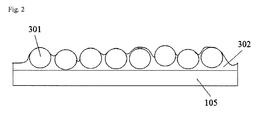
- FIG. 2 shows an illustrative shape in which a scattering layer including scattering particles 301 is formed on a base layer 105.
- the scattering layer of FIG. 2 includes scattering particles 301 and a binder 302.
- scattering particles may refer to, for example, particles having a different refractive index from that of the binder for forming the scattering layer or a planarizing layer to be described later. These particles may have a refractive index of 1.0 to 3.5, for example, approximately 1.0 to 2.0, 1.2 to 1.8, 2.1 to 3.5 or 2.2 to 3.0, and an average diameter of approximately 50 to 20,000 or 100 to 5,000 nm.
- the particles may have a spherical, oval, polygonal or amorphous shape, but the present application is not particularly limited thereto.
- the scattering particles may include, for example, an organic material such as polystyrene or a derivative thereof, an acrylic resin or a derivative thereof, a silicon resin or a derivative thereof, or a novolac resin or a derivative thereof, or an inorganic material such as silica, alumina, titanium oxide or zirconium oxide.
- the scattering particles may include any one of the above materials, or at least two thereof, or may be formed in core/shell-type particles or hollow-type particles as needed.
- the scattering layer may further include a binder for maintaining the scattering particles.
- a binder for maintaining the scattering particles, another adjacent material, for example, a material having the same refractive index as that of the base layer 105 may be used.
- a heat- or photo-curable monomeric, oligomeric, or polymeric organic material including polyimide, a caldo resin having a fluorene ring, urethane, epoxide, polyester, or acrylate, an inorganic material such as silicon oxide, silicon nitride, silicon oxynitride, or polysiloxane, or an organic/inorganic combination material.
- the scattering layer may be, for example, a layer having an uneven structure.
- FIG. 3 exemplarily shows that a scattering layer 401 having an uneven structure is formed on a base layer 105.
- incident light may be scattered.
- the scattering layer having an uneven structure may be formed, for example, by coating a heat- or photo-curable material, and curing the material in contact with a mold capable of transferring a desired shape of the uneven structure during curing or performing an etching process.
- the scattering layer may be formed by blending particles having a suitable size and shape in a binder for forming the scattering layer. In this case, the particles may not need to be particles having a scattering function, but particles having a scattering function may also be used.
- the scattering layer may be formed by coating a material by wet coating, and performing application of heat or irradiation of light, curing of the material by a sol-gel method, a deposition method such as a chemical vapor deposition (CVD) or physical vapor deposition (PVD) method, or a microembossing method.
- a deposition method such as a chemical vapor deposition (CVD) or physical vapor deposition (PVD) method, or a microembossing method.
- the OLED may further include a planarizing layer formed on the top of the scattering layer.
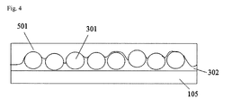
- FIGS. 4 and 5 exemplarily show OLEDs further including a planarizing layer.
- FIG. 4 shows that a planarizing layer 501 is formed on the scattering layer having the structure shown in FIG.2
- FIG. 5 shows that a planarizing layer 501 is formed on the scattering layer having the structure shown in FIG. 3 .
- the planarizing layer provides a surface on which the electrode layer such as the hole injection electrode layer may be formed on the scattering layer, and in some case, may embody more excellent light extraction efficiency through interaction with the scattering layer.
- the planarizing layer may, for example, have the same refractive index as that of the adjacent electrode layer, for example, approximately 1.8 to 3.5 or 2.2 to 3.0.
- the planarizing layer may be formed by, for example, a method of mixing high refractive particles having a high refractive index and an average diameter of approximately 1 to 100, 10 to 90, 20 to 80, 30 to 70, 30 to 60 or 30 to 50 nm with a binder for forming the planarizing layer.
- a binder for forming the planarizing layer for example, alumina, titanium oxide or zirconium oxide may be used.
- titanium oxide for example, rutile-type titanium oxide may be sued.
- the rutile-type titanium oxide may have a higher refractive index than those of other particles, and thus even though a content of the high refractive particles in the material for forming the planarizing layer is relatively small, the planarizing layer may have a high refractive index.
- the ratio of the high refractive particles is relatively low in the material, a higher quality of planarizing layer may be embodied.
- the planarizing layer may also be formed using a material prepared by blending a compound such as an alkoxide or acylate of a metal such as zirconium, titanium or cesium with a binder having a polar group such as a carboxylic group or a hydroxyl group.
- the compound such as an alkoxide or acrylate may be condensed with the polar group of the binder, and provide the metal to a backbone of the binder, thereby embodying a highly refractive index.
- Examples of the alkoxide or acrylate compound may include a titanium alkoxide such as tetra-n-butoxy titanium, tetraisopropoxy titanium, tetra-n-propoxy titanium or tetraethoxy titanium, a titanium acylate such as titanium stearate, a titanium chelate, a zirconium alkoxide such as tetra-n-butoxy zirconium, tetra-n-propoxy zirconium, tetraisopropoxy zirconium or tetraethoxy zirconium, a zirconium acylate such as zirconium tributoxystearate, or a zirconium chelate.
- suitable one selected from the binders described in the category of the scattering layer may be used.
- planarizing layer may be formed by preparing a coating solution by blending a metal alkoxide such as titanium alkoxide or zirconium alkoxide with a solvent such as alcohol or water, coating the coating solution, and plasticizing the coated solution at a suitable temperature by sol-gel coating.
- a metal alkoxide such as titanium alkoxide or zirconium alkoxide
- a solvent such as alcohol or water
- the scattering layer or the planarizing layer may have a smaller projected area than that of the hole or electron injection electrode layer formed thereon.
- the scattering layer or the scattering layer and planarizing layer may also have a smaller projected area than that of the base layer.
- projected area used herein refers to a projected area of a target recognized when the substrate is observed from above or below in a direction parallel to a normal line of a surface thereof, for example, an area of the base layer, the scattering layer or the electrode layer.
- the scattering layer has a smaller projected area than that of the electrode layer.
- the scattering layer may be present in various types when it has a smaller projected area than those of the base layer and the electrode layer.
- the scattering layer 104 as shown in FIG. 6 , may be formed only in a part other than an edge of the base layer 105, or as shown in FIG. 7 , may partially remain on an edge of the base layer 105.
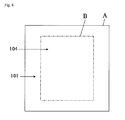
- FIG. 8 exemplarily shows that the scattering layer of FIG. 6 is observed from above.
- an area (A), that is, a projected area (A), of the electron or hole injection electrode layer 101 recognized when the scattering layer is observed from above is larger than that of a projected area (B) of the scattering layer 104 disposed therebelow.
- a ratio (A/B) of the projected area (A) of the electrode layer 101 and the projected area (B) of the scattering layer may be, for example, 1.04, 1.06, 1.08, 1.1, or 1.15 or more.
- the upper limit of the ratio (A/B) in projected area is not particularly limited.
- the upper limit of the ratio (A/B) may be, for example, approximately 2.0, 1.5, 1.4, 1.3 or 1.25.
- the electron injection or hole injection electrode layer may be formed on the top of the base layer on which the scattering layer is not formed.
- the electrode layer may be formed in contact with the base layer, or an additional component may be further included between the electrode layer and the base layer. According to such a structure, a structure in which the scattering layer is not exposed to an external environment may be embodied.
- the electron injection or hole injection electrode layer may be formed in a region including a region beyond all peripheral regions of the scattering layer when observed from above.
- the electrode layer 101 may be formed up to the region including the region beyond all the peripheral regions of at least one scattering layer, for example, the scattering layer on which an organic layer will be formed at least the top thereof.
- the structure of FIG. 7 when the organic layer is formed on the top of the scattering layer present on the right and left edges, the structure of FIG.
- the electrode 7 may be changed to form the electrode layer up to the region beyond all the peripheral regions of the scattering layer present on the right and left edge by extending to left and right sides.
- a structure in which the scattering layer is not exposed to an external environment may be formed. Accordingly, penetration of external moisture or oxygen through the highly refractive layer and the like may be prevented, an adhesive strength between the encapsulating structure or the electrode and the substrate may be stably ensured, and a surface hardness at the edge of the device may be excellently maintained.
- Controlling of the projected area may be performed by, for example, forming the electrode layer to have a larger projected area than that of the scattering layer during a deposition or sputtering process for forming the electrode layer, and when necessary, by removing a predetermined part of the scattering layer and/or planarizing layer to pattern.
- the OLED may be present in a suitable encapsulating structure to prevent moisture or oxygen from an external environment. That is, the OLED may further include an encapsulating structure for protecting the electrode layer and the organic stacked structure.
- the encapsulating structure may be, for example, a can such as a glass can or a metal can, or a film covering an entire surface of the organic stacked structure.
- FIG. 9 exemplarily shows that a can-type encapsulating structure 901 such as a glass can or a metal can is further included as an encapsulating structure 901 for projecting an electron injection electrode layer 102 and an organic stacked structure 103, which are sequentially formed.
- the encapsulating structure 901 may be, for example, attached to a hole injection electrode layer 101 by an adhesive 902.
- the encapsulating structure may be, for example, adhered to the hole injection electrode layer 101 below which a scattering layer 104 is not present.
- the encapsulating structure 901 may be attached to the electrode layer 101 present on an edge of a base layer 105 by the adhesive 902. In this manner, a protective effect by the encapsulating structure may be optimized.
- the encapsulating structure may be, for example, a film coating entire surfaces of the organic stacked structure and the electron injection electrode layer.
- FIG. 10 shows an illustrative film-type encapsulating structure 1001 covering entire surfaces of an organic stacked structure 103 and an electron injection electrode layer.
- the film-type encapsulating structure 1001 may have a structure coating the entire surfaces of the organic stacked structure 103 and the electrode layer 102, and adhered to a second substrate 1002 on the top of a base layer 105 having a scattering layer 104 and a hole injection electrode layer 101.
- the second substrate 1002 for example, a glass substrate, a metal substrate, a polymer film or a barrier layer may be used.
- the film-type encapsulating structure may be formed by, for example, coating a liquid material cured by heat or UV radiation such as an epoxy resin and curing the liquid material, or laminating the substrate with the upper substrate using an adhesive sheet previously manufactured in a film type using the epoxy resin.
- the encapsulating structure may include a water adsorbent or getter such as a metal oxide such as calcium oxide or beryllium oxide, a metal halide such as calcium oxide, or phosphorus pentoxide, when necessary.
- a water adsorbent or getter such as a metal oxide such as calcium oxide or beryllium oxide, a metal halide such as calcium oxide, or phosphorus pentoxide, when necessary.
- the water adsorbent or getter may be included in the film-type encapsulating structure, or present at a predetermined position of a can-type encapsulating structure.
- the encapsulating structure may further include a barrier film or a conductive film.
- the encapsulating structure may be attached to, for example, the top of the hole injection electrode layer 101 below which the scattering layer 104 is not formed.
- a sealing structure in which the scattering layer and the like are not exposed to an external environment may be embodied.
- the sealing structure may refer to, for example, a state in which the entire surface of the scattering layer is not exposed to an external environment by being surrounded by the base layer, the electrode layer and/or the encapsulating structure, or by being surrounded by the sealing structure formed to include the base layer, the electrode layer and/or the encapsulating structure.
- the sealing structure may be formed to only include the base layer, the electrode layer and/or the encapsulating structure, or to include the base layer, the electrode layer, the encapsulating structure, and also another component, for example, a conductive material or an intermediate layer as long as the highly refractive layer is not exposed to an external environment.
- another component may be present at a part in which the base layer 105 is in contact with the electrode layer 101 or the electrode layer 101 is in contact with the encapsulating structure 901 or 1001 or another position.
- an organic, inorganic or organic/inorganic combination material having a low water permeability, an insulating layer or an auxiliary electrode layer may be used.
- the OLED may be effectively applied to a backlight of a liquid crystal display (LCD), lightings, sensors, printers, a light source of a copy machine, a light source for an automobile gauge, a signal light, a pilot lamp, a display device, a light source for a planar emitting device, a display, decorations or other kinds of lights.
- the present application relates to a lighting device including the OLED.
- other components constituting the device or a method of constituting the device is not particularly limited, but all of arbitrary materials or methods known in the related art may be employed as long as these are used in the OLED.
- An illustrative OLED of the present application can minimize light absorption of a reflective electrode layer and evanescent coupling by surface plasmon, and exhibit excellent emitting efficiency.
- a sol-gel coating solution was prepared by sufficiently dispersing 1 g of polymer beads (XX75BO, average diameter: approximately 3 ⁇ m, Sekisui) in 10 g of tetramethoxy silane. Subsequently, a scattering layer was formed by coating the prepared coating solution on a glass substrate and performing a sol-gel reaction.
- a planarizing layer having a refractive index of approximately 1.8 was formed by coating a highly refractive coating solution prepared by blending highly refractive titanium oxide particles having an average diameter of approximately 10 nm and a refractive index of approximately 2.5 in the sol-gel coating solution including tetramethoxy silane in the same manner as described above on the top of the scattering layer, and performing a sol-gel reaction in the same manner as in described above. Subsequently, the light scattering layer and the planarizing layer were partially removed by radiating a laser to the formed layer such that positions of the remaining light scattering layer and the planarizing layer corresponded to an emitting region of an organic layer to be subsequently formed.
- a hole injection electrode layer including ITO was formed on the entire surface of the glass substrate to have a predetermined thickness by a known sputtering method. Subsequently, a hole injection layer including N,N'-Di-[(1-naphthyl)-N,N'-diphenyl]-1,1'-biphenyl)-4,4'-diamine ( ⁇ -NPD) and an emitting layer (4,4',4"-tris(N-carbazolyl)-triphenylamine (TCTA):Firpic, TCTA:Fir6) were sequentially formed by a known deposition method.
- a low refractive organic layer was then formed to a thickness of approximately 70 nm by codepositing an electron transport compound, 4,4',4"-tris(N-carbazolyl)-triphenylamine (TCTA) and a low refractive material, LiF (refractive index: approximately 1.39) on the top of the emitting layer to have a refractive index of the entire layer of approximately 1.66.
- TCTA 4,4',4"-tris(N-carbazolyl)-triphenylamine
- LiF refractive index: approximately 1.39
- a device was manufactured by forming an aluminum (Al) electrode as the electron injection reflective electrode on the top of the low refractive organic layer by a vacuum deposition method.
- a system was manufactured by attaching an encapsulating structure to the device in a glove box at an Ar gas atmosphere.
- a voltage-current characteristic, luminescence and efficiency were measured when a current density was 3mAcm -2 from a Half Moon. Meanwhile, here, a refractive index was a value measured in a wavelength of approximately 550 nm using an ellipsometer produced by Nanoview.
- An OLED was manufactured as described in Example 1, except that a layer of only an electron transport compound, TCTA was formed on an emitting layer to have a thickness of approximately 70 nm instead of a low refractive organic layer.
- An OLED was manufactured as described in Example 1, except that a scattering layer and a planarizing layer were not formed.
- An OLED was manufactured as described in Example 1, except that a scattering layer and a planarizing layer were not formed, and a layer of only an electron transport compound, TCTA was formed on an emitting layer to have a thickness of approximately 70 nm instead of a low refractive organic layer.
- An OLED was manufactured as described in Example 1, except that a codeposition layer of an electron transport compound, TCTA, and yttrium oxide (Y 2 O 3 ) having a refractive index of approximately 1.79 was formed on an emitting layer to have a thickness of approximately 70 nm instead of a low refractive organic layer.
- a codeposition layer of an electron transport compound, TCTA, and yttrium oxide (Y 2 O 3 ) having a refractive index of approximately 1.79 was formed on an emitting layer to have a thickness of approximately 70 nm instead of a low refractive organic layer.
- An OLED was manufactured as described in Example 1, except that a layer of only an electron transport compound, TCTA was formed on an emitting layer to have a thickness of approximately 20 nm instead of a low refractive organic layer.
Landscapes
- Physics & Mathematics (AREA)
- Optics & Photonics (AREA)
- Engineering & Computer Science (AREA)
- Manufacturing & Machinery (AREA)
- Electromagnetism (AREA)
- Electroluminescent Light Sources (AREA)
Abstract
Description
- The present application relates to an organic light emitting device (OLED) and lighting.
- Conventionally, an OLED sequentially includes a substrate, a first electrode layer, an organic layer including an emitting layer and a second electrode layer.
- In a structure known as a bottom emitting device, the first electrode layer may be a transparent electrode layer, and the second electrode layer may be a reflective electrode layer. In addition, in a structure known as a top emitting device, the first electrode layer may be formed as a reflective electrode layer, and the second electrode layer may be formed as a transparent electrode layer.
- Electrons and holes are injected respectively by the two electrode layers, the injected electrons and holes are recombined in the emitting layer located in the emitting layer, resulting in generating light. The light may be emitted toward the substrate in the bottom emitting device, or toward the second electrode layer in the top emitting device.
- In the structure of the OLED, indium tin oxide (ITO) generally used as the transparent electrode layer, the organic layer, and the substrate, which is conventionally formed of glass, have refractive indexes of approximately 2.0, 1.8, and 1.5, respectively. In such a relationship of the refractive index, for example, the light generated in the organic emitting layer in the bottom emitting device is trapped at an interface between the organic layer and the first electrode layer or in the substrate due to a total internal reflection phenomenon, and only a very small amount of light is emitted.
- The present application is directed to providing an OLED and lighting.
- One aspect of the present application provides an illustrative OLED, including: an electron injection electrode layer and a hole injection electrode layer. In the OLED, the electron injection electrode layer and the hole injection electrode layer may face each other, and an organic stacked structure may be present therebetween. The organic stacked structure may be a stacked structure including at least one layer including a functional organic material. The organic stacked structure may include a low refractive organic layer. The term "low refractive organic layer" used herein may refer to a layer having an organic compound and a refractive index of 1.7 or less. The term "refractive index" used herein may refer to, unless particularly defined otherwise, a refractive index with respect to light having a wavelength of approximately 550 to 633 nm. The organic stacked structure may include an emitting layer along with the low refractive organic layer.
- The OLED may include a scattering layer. The scattering layer may be formed in contact with or adjacent to one surface of, for example, the electron or hole injection electrode layer, particularly, the hole injection electrode layer. Here, one surface of the electrode layer in contact with or adjacent to the scattering layer may be a surface opposite to the surface of the electrode layer in contact with or adjacent to the organic stacked structure.
- In one embodiment, the OLED may further include a base layer. On the top of the base layer, a structure in which the electron or hole injection electrode layer, the organic stacked structure and the hole or electron injection electrode layer are sequentially formed may be formed. In this structure, the scattering layer may be disposed between the base layer and the electron or hole injection electrode layer formed on the top of the base layer.
-
FIG. 1 shows astructure 100 of an illustrative OLED, in which a holeinjection electrode layer 101, an organicstacked structure 103 and an electroninjection electrode layer 102 are sequentially stacked on abase layer 105, and ascattering layer 104 is formed between the holeinjection electrode layer 101 and the base layer. The organic stackedstructure 103 includes a low refractiveorganic layer 1031 and anemitting layer 1032. - As the base layer, a suitable material may be selected according to necessity without particular limitation. In one embodiment, the OLED may be a bottom emitting device, and in this case, the base layer may be a transparent base layer, for example, a base layer having transmittance of 50, 60, 70, 80 or 90% or more with respect to light having a wavelength in a visible region. As the transparent base layer, a glass base layer or a transparent polymer base layer may be used. As the glass base layer, a base layer including soda lime glass, barium/strontium-containing glass, lead glass, alumino silicate glass, borosilicate glass, barium borosilicate glass, or quartz may be used, and as the polymer base layer, a base layer including polycarbonate (PC), an acryl resin, poly(ethylene terephthalate) (PET), poly(ether sulfide) (PES), or polysulfone (PS) may be used, but the present application is not limited thereto. As needed, the base layer may be a TFT substrate having a drive TFT.
- The hole injection electrode layer may be formed using, for example, a transparent conductive material having a relatively highly work function. For example, the hole injection electrode layer may include a metal, an alloy, an electric conductive compound having a work function of approximately 4.0 eV or more, or a mixture of at least two thereof. Such a material may be a conductive transparent material, for example, a metal such as gold, CuI, indium tin oxide (ITO), indium zinc oxide (IZO), ZnO, SnO2 or In2O3. The hole injection electrode layer may be formed by, for example, vacuum deposition or sputtering using the above material. The hole injection electrode layer may have, for example, light transmittance of 10% or more, and a surface resistance of several hundreds of Ω/sq or less, for example, 100 Ω/sq or less. A thickness of the hole injection electrode layer may be dependent on light transmittance or surface resistance, but may conventionally be 50 to 150 nm or 10 to 200 nm.
- The electron injection electrode layer may be formed using, for example, a material having a relatively small work function. As such a material, a metal such as potassium, lithium, sodium, magnesium, lanthanium, cesium, calcium, strontium, barium, aluminum, silver, indium, tin, zinc or zirconium or an alloy of two or more components selected therefrom, for example, a magnesium/indium alloy, a magnesium/aluminum alloy, an aluminum/lithium alloy, an aluminum/scandium/lithium alloy, a magnesium/silver alloy or an aluminum/calcium alloy may be used. The electron injection electrode layer may be formed using, for example, deposition or sputtering.
- In the illustrative OLED, among the electron and hole injection electrode layers, an electrode layer formed on the base layer may be a transparent electrode layer, and an electrode layer formed on the organic stacked structure may be a reflective electrode layer.
- The organic stacked structure at least includes a low refractive organic layer and an emitting layer.
- The low refractive organic layer may be a layer including an organic compound, for example, having a refractive index of 1.7 or less, less than 1.7, 1.68, 1.66, 1.65, 1.63, 1.60, 1.55 or 1.52 or less. Here, the lower limit of the refractive index of the low refractive organic layer may be, but is not particularly limited to, for example, 0.5 or 0.7 or more.
- In one embodiment, the low refractive organic layer may be formed in contact with or adjacent to an electron or hole injection electrode layer formed as a reflective electrode layer, for example, an electron injection electrode layer formed as a reflective electrode layer. The low refractive organic layer formed at this position may reduce the influence of light absorption of the reflective electrode layer by an organic interaction with the scattering layer and evanescent coupling by surface plasmon, and increase light extraction efficiency of the device.
- When the electrode in contact with or adjacent to the low refractive organic layer is an electron injection electrode layer, an organic compound included in the low refractive organic layer may be an electron accepting organic compound. The low refractive organic layer including the electron accepting organic compound may serve as an electron injection layer, an electron transport layer, or an electron injection/transport layer.
- As the electron accepting organic compound, a known arbitrary compound may be used without particular limitation. As such an organic compound, an aromatic amine compound such as 4,4',4"-tri(N-carbazolyl)triphenylamine; a polycyclic compound such as p-terphenyl or quaterphenyl or a derivative thereof; a polycyclic hydrocarbon compound such as naphthalene, tetracene, pyrene, coronene, chrysene, anthracene, diphenylanthracene, naphthacene, or phenanthrene or a derivative thereof; or a heterocyclic compound such as phenanthroline, bathophenanthroline, phenanthridine, acridine, quinoline, quinoxaline, or phenazine or a derivative thereof. In addition, fluoroceine, perylene, phthaloperylene, naphthaloperylene, perynone, phthaloperynone, naphthaloperynone, diphenylbutadiene, tetraphenylbutadiene, oxadiazole, aldazine, bisbenzoxazoline, bisstyryl, pyrazine, cyclopentadiene, oxine, aminoquinoline, imine, diphenylethylene, vinylanthracene, diaminocarbazole, pyrane, thiopyrane, polymethine, merocyanine, quinacridone, rubrene or a derivative thereof, a metal chelate complex compound disclosed in a patent publication such as Japanese Patent Application Laid-Open No.
1988-295695 1996-22557 1996-81472 1993-009470 1993-017764 1993-202011 1995-179394 1995-278124 1995-228579 1995-157473 1994-203963 1994-132080 1994-88072 1994-100857 1994-207170 1994-49079 1994-293778 1994-279322 1994-279323 1994-107648 1994-092947 1994-206865 1994-145146 1992-96990 1991-296595 1990-191694 1990-196885 1990-255789 1990-289676 1990-88689 1990-250292 - The organic compound may conventionally have a refractive index of approximately 1.7 to 1.8. To maintain the refractive index of the low refractive organic layer including such an organic compound at a low level, the low refractive organic layer may include a material having a low refractive index (hereinafter, referred to as a low refractive material) along with the organic compound. As such a low refractive material, for example, a material having a refractive index of 1.60 or less may be used. The lower limit of the refractive index of the low refractive material may be, but is not particularly limited to, for example, 0.5 or 0.7 or more. As the material, one or a mixture of at least two selected from lithium fluoride (LiF), magnesium fluoride (MgF2), potassium fluoride (KF), sodium fluoride (NaF), aluminum fluoride (AlF2), barium fluoride (BaF2), beryllium fluoride (BeF2), cadmium fluoride (CdF2), calcium fluoride (CaF2), cesium fluoride (CsF), thorium fluoride (ThF4), yttrium fluoride (YF3), iron fluoride (FeCl2), vanadium fluoride (V2O5) and Na2Al3F14 (Chiolite) may be used.
- A content of the low refractive material included in the low refractive organic layer is not particularly limited as long as the low refractive organic layer is controlled to have a refractive index in the above-described range. In one embodiment, the low refractive material may be included at 150, 140, 130, 120, 110 or 100 parts by weight with respect to 100 parts by weight of the organic compound included in the low refractive organic layer. The unit "parts by weight" used herein refers to, unless particularly defined otherwise, a weight ratio between components. The lower limit of the ratio of the low refractive material is determined by the refractive index of the low refractive organic layer and thus is not particularly limited.
- The low refractive organic layer including the organic compound and the low refractive material as described above may be formed by, for example, a codeposition method using the organic compound and the low refractive material.
- The low refractive organic layer may have a thickness of, for example, 15, 18, 20, 30, 40, 50, 55, 60, 65 or 70 nm or more. In this range, the avenescent effect of the device may be minimized and light extraction efficiency may be optimized. The upper limit of the thickness of the low refractive organic layer is not particularly limited. For example, the low refractive organic layer may have a thickness of 150, 100 or 85 nm or less.
- The emitting layer may be formed using, for example, various fluorescent or phosphorescent organic materials known in the art. The emitting layer may also be formed by employing the electron accepting organic compound described above or suitable one exhibiting an emitting characteristic selected from electron donating organic compounds to be described later.
- The material for the emitting layer may be, but is not limited to, a fluorescent material such as an Alq-based material such as tris(4-methyl-8-quinolinolate)aluminum(III) (Alg3), 4-MAlq3 or Gaq3; a cyclopenadiene derivative such as C-545T(C26H26N2O2S DSA-amine, TBSA, BTP, PAP-NPA, spiro-FPA, Ph3Si (PhTDAOXD), 1,2,3,4,5-pentaphenyl-1,3-cyclopentadiene (PPCP), 4,4'-bis(2,2'-diphenylyinyl)-1,1'-biphenyl (DPVBi), distyryl benzene or a derivative thereof, or 4-(dicyanomethylene)-2-tert-butyl-6-(1,1,7,7,-tetramethyljulolidyl-9-enyl)-4H-pyran (DCJTB), DDP, AAAP or NPAMLI; or a phosphorescent material such as Firpic, m-Firpic, N-Firpic, bon2Ir(acac), (C6)2Ir(acac), bt2Ir(acac), dp2Ir(acac), bzq2Ir(acac), bo2Ir(acac), F2Ir(bpy), F2Ir(acac), op2Ir(acac), ppy2Ir(acac), tpy2Ir(acac), fac-tris[2-(4,5'-difluorophenyl)pyridine-C'2,N] iridium(III) (FIrppy) or bis(2-(2'-benzo[4,5-a]thienyl)pyridinato-N,C3') iridium(acetylactonate) (Btp2Ir(acac)). The emitting layer may include the material as a host, and a host-dopant system including perylene, distyrylbiphenyl, DPT, quinacridone, rubrene, BTX, ABTX or DCJTB as a dopant.
- The organic stacked structure may be present in various types including another layer known in the art, as long as it includes at least the low refractive organic layer and the emitting layer.
- For example, when the lowly organic layer includes an electron accepting organic compound, and thus serves as an electron transport layer, as a layer further included in the organic stacked structure, a hole injection layer (HIL), a hole transport layer (HTL), an electron injection layer (EIL) or a hole blocking layer (HBL) may be used.
- Here, the hole injection layer may be a layer further included in contact with the hole injection electrode layer to assist smooth injection of holes into the organic stacked structure from the electrode layer. In addition, the hole transport layer may be present, for example, between the emitting layer and the hole injection electrode layer and have a higher level of highest occupied molecular orbital (HOMO) than that of the emitting layer, thereby assisting smooth transport of holes.
- The hole injection or hole transport layer may include, for example, an electron donating organic compound. As the electron donating organic compound, N,N',N'-tetraphenyl-4,4'-diaminophenyl, N,N'-diphenyl-N,N'-di(3-methylphenyl)-4,4'-diaminobiphenyl, 2,2-bis(4-di-p-tollylaminophenyl)propane, N,N,N',N'-tetra-p-tollyl-4,4'-diaminobiphenyl, bis(4-di-p-tollylaminophenyl)phenylmethane, N,N'-diphenyl-N,N'-di(4-methoxyphenyl)-4,4'-diaminobiphenyl, N,N,N',N'-tetraphenyl-4,4'-diaminodiphenylether, 4,4'-bis(diphenylamino)quadriphenyl, 4-N,N-diphenylamino-(2-diphenylvinyl)benzene, 3-methoxy-4'-N,N-diphenylaminostyrylbenzene, N-phenylcarbazole, 1,1-bis(4-di-p-triaminophenyl)cyclohexane, 1,1-bis(4-di-p-triaminophenyl)-4-phenylcyclohexane, bis(4-dimethylamino-2-methylphenyl)phenylmethane, N,N,N-tri(p-tollyl)amine, 4-(di-p-tollylamino)-4'-[4-(di-p-tollylamino)styryl]stilbene, N,N,N',N'-tetraphenyl-4,4'-diaminobiphenyl N-phenylcarbazole, 4,4'-bis[N-(1-naphthyl)-N-phenyl-amino]biphenyl, 4,4"-bis[N-(1-naphthyl)-N-phenylamino]p-terphenyl, 4,4'-bis[N-(2-naphthyl)-N-phenylamino]biphenyl, 4,4'-bis[N-(3-acenaphthenyl)-N-phenylamino]biphenyl, 1,5-bis[N-(1-naphthyl)-N-phenylamino]naphthalene, 4,4'-bis[N-(9-anthryl)-N-phenylamino]biphenylphenylamino]biphenyl, 4,4"-bis[N-(1-anthryl)-N-phenylamino]-p-terphenyl, 4,4'-bis[N-(2-phenanthryl)-N-phenylamino]biphenyl, 4,4'-bis[N-(8-fluoranthenyl)-N-phenylamino]biphenyl, 4,4'-bis[N-(2-pyrenyl)-N-phenylamino]biphenyl, 4,4'-bis[N-(2-perylenyl)-N-phenylamino]biphenyl, 4,4'-bis[N-(1-coronenyl)-N-phenylamino]biphenyl, 2,6-bis(di-p-tollylamino)naphthalene, 2,6-bis[di-(1-naphthyl)amino]naphthalene, 2,6-bis[N-(1-naphthyl)-N-(2-naphthyl)amino]naphthalene, 4,4"-bis[N,N-di(2-naphthyl)amino]terphenyl, 4,4-bis {N-phenyl-N-[4-(1-naphthyl)phenyl]amino}biphenyl, 4,4'-bis[N-phenyl-N-(2-pyrenyl)amino]biphenyl, 2,6-bis[N,N-di-(2-naphthyl)amino]fluorine or 4,4"-bis(N,N-di-p-tollylamino)terphenyl, or an aryl amine compound such as bis(N-1-naphthyl)(N-2-naphthyl)amine may be used, but the present application is not limited thereto.
- The hole injection layer or hole transport layer may be formed by dispersing the organic compound in a polymer, or using a polymer derived from the organic compound. In addition, a π-conjugated polymer such as polyparaphenylenevinylene and a derivative thereof, a hole transport non-conjugated polymer such as poly(N-vinylcarbazole) or a σ-conjugated polymer of polysilane may also be used.
- The hole injection layer may be formed using an electrically-conductive polymer such as a metal phthalocyanine such as copper phthalocyanine or a non-metal phthalocyanine, a carbon layer and polyaniline, or may be formed by reaction with a Lewis acid using the aryl amine compound as an oxidizing agent.
- The electron injection layer may be a layer for assisting injection of electrons into the organic stacked structure from the electrode layer, and may be further included in contact with the electron injection electrode layer when necessary. The electron injection layer may be formed using a known material such as LiF or CsF. The hole blocking layer may be a layer capable of enhancing a life span and efficiency of the device by preventing approach of holes injected from the hole injection electrode layer to the electron injection electrode layer through the emitting layer, and may be formed in a suitable part between the emitting layer and the electron injection electrode layer using a known material when necessary.
- The organic stacked structure may be formed in various structures. For example, when the low refractive organic layer serves as an electron transport layer, the organic stacked structure may include: an emitting layer and a low refractive organic layer; an emitting layer, a low refractive organic layer and an electron injection layer; a hole transport layer, an emitting layer and a low refractive organic layer; a hole injection layer, a hole transport layer, emitting layer and a low refractive organic layer; a hole transport layer, emitting layer, a hole blocking layer and a low refractive organic layer; a hole injection layer, a hole transport layer, emitting layer, a hole blocking layer and a low refractive organic layer; a hole transport layer, emitting layer, a low refractive organic layer and an electron injection laye; or a hole injection layer, a hole transport layer, emitting layer, a low refractive organic layer and an electron injection layer, which are sequentially formed from the hole injection electrode layer, but the present application is not limited thereto. When necessary, the organic stacked structure may have a structure including at least two emitting layers. The structure including at least two emitting layers may include at least two emitting layers divided by an inter-electrode layer having a charge generating characteristic or a charge generating layer (CGL) are present at a suitable position in the organic stacked structure, but the present application is not limited thereto.
- The OLED may also include a scattering layer. The scattering layer may be a layer capable of increasing the light extraction efficiency of the device through interaction with the low refractive organic layer, and may be formed using any known material and structure as long as they serve to scatter incident light.
- In one embodiment, the scattering layer may be a layer including scattering particles.
FIG. 2 shows an illustrative shape in which a scattering layer including scatteringparticles 301 is formed on abase layer 105. The scattering layer ofFIG. 2 includes scatteringparticles 301 and abinder 302. - The term "scattering particles" used herein may refer to, for example, particles having a different refractive index from that of the binder for forming the scattering layer or a planarizing layer to be described later. These particles may have a refractive index of 1.0 to 3.5, for example, approximately 1.0 to 2.0, 1.2 to 1.8, 2.1 to 3.5 or 2.2 to 3.0, and an average diameter of approximately 50 to 20,000 or 100 to 5,000 nm. The particles may have a spherical, oval, polygonal or amorphous shape, but the present application is not particularly limited thereto. The scattering particles may include, for example, an organic material such as polystyrene or a derivative thereof, an acrylic resin or a derivative thereof, a silicon resin or a derivative thereof, or a novolac resin or a derivative thereof, or an inorganic material such as silica, alumina, titanium oxide or zirconium oxide. The scattering particles may include any one of the above materials, or at least two thereof, or may be formed in core/shell-type particles or hollow-type particles as needed.
- The scattering layer may further include a binder for maintaining the scattering particles. As the binder, as a material capable of maintaining the scattering particles, another adjacent material, for example, a material having the same refractive index as that of the
base layer 105 may be used. As the binder, for example, a heat- or photo-curable monomeric, oligomeric, or polymeric organic material including polyimide, a caldo resin having a fluorene ring, urethane, epoxide, polyester, or acrylate, an inorganic material such as silicon oxide, silicon nitride, silicon oxynitride, or polysiloxane, or an organic/inorganic combination material. - The scattering layer may be, for example, a layer having an uneven structure.
FIG. 3 exemplarily shows that ascattering layer 401 having an uneven structure is formed on abase layer 105. When the uneven structure of the scattering layer is suitably controlled, incident light may be scattered. - The scattering layer having an uneven structure may be formed, for example, by coating a heat- or photo-curable material, and curing the material in contact with a mold capable of transferring a desired shape of the uneven structure during curing or performing an etching process. In another method, the scattering layer may be formed by blending particles having a suitable size and shape in a binder for forming the scattering layer. In this case, the particles may not need to be particles having a scattering function, but particles having a scattering function may also be used.
- For example, the scattering layer may be formed by coating a material by wet coating, and performing application of heat or irradiation of light, curing of the material by a sol-gel method, a deposition method such as a chemical vapor deposition (CVD) or physical vapor deposition (PVD) method, or a microembossing method.
- The OLED may further include a planarizing layer formed on the top of the scattering layer.
FIGS. 4 and5 exemplarily show OLEDs further including a planarizing layer.FIG. 4 shows that aplanarizing layer 501 is formed on the scattering layer having the structure shown inFIG.2 , andFIG. 5 shows that aplanarizing layer 501 is formed on the scattering layer having the structure shown inFIG. 3 . - The planarizing layer provides a surface on which the electrode layer such as the hole injection electrode layer may be formed on the scattering layer, and in some case, may embody more excellent light extraction efficiency through interaction with the scattering layer. The planarizing layer may, for example, have the same refractive index as that of the adjacent electrode layer, for example, approximately 1.8 to 3.5 or 2.2 to 3.0.
- The planarizing layer may be formed by, for example, a method of mixing high refractive particles having a high refractive index and an average diameter of approximately 1 to 100, 10 to 90, 20 to 80, 30 to 70, 30 to 60 or 30 to 50 nm with a binder for forming the planarizing layer. As the high refractive particles, for example, alumina, titanium oxide or zirconium oxide may be used. In one embodiment, as the high refractive particles, titanium oxide, for example, rutile-type titanium oxide may be sued. The rutile-type titanium oxide may have a higher refractive index than those of other particles, and thus even though a content of the high refractive particles in the material for forming the planarizing layer is relatively small, the planarizing layer may have a high refractive index. When the ratio of the high refractive particles is relatively low in the material, a higher quality of planarizing layer may be embodied.
- In another embodiment, the planarizing layer may also be formed using a material prepared by blending a compound such as an alkoxide or acylate of a metal such as zirconium, titanium or cesium with a binder having a polar group such as a carboxylic group or a hydroxyl group. The compound such as an alkoxide or acrylate may be condensed with the polar group of the binder, and provide the metal to a backbone of the binder, thereby embodying a highly refractive index. Examples of the alkoxide or acrylate compound may include a titanium alkoxide such as tetra-n-butoxy titanium, tetraisopropoxy titanium, tetra-n-propoxy titanium or tetraethoxy titanium, a titanium acylate such as titanium stearate, a titanium chelate, a zirconium alkoxide such as tetra-n-butoxy zirconium, tetra-n-propoxy zirconium, tetraisopropoxy zirconium or tetraethoxy zirconium, a zirconium acylate such as zirconium tributoxystearate, or a zirconium chelate. In addition, as the binder having a polar group, suitable one selected from the binders described in the category of the scattering layer may be used.
- In addition, the planarizing layer may be formed by preparing a coating solution by blending a metal alkoxide such as titanium alkoxide or zirconium alkoxide with a solvent such as alcohol or water, coating the coating solution, and plasticizing the coated solution at a suitable temperature by sol-gel coating.
- The scattering layer or the planarizing layer may have a smaller projected area than that of the hole or electron injection electrode layer formed thereon. The scattering layer or the scattering layer and planarizing layer may also have a smaller projected area than that of the base layer. The term "projected area" used herein refers to a projected area of a target recognized when the substrate is observed from above or below in a direction parallel to a normal line of a surface thereof, for example, an area of the base layer, the scattering layer or the electrode layer. Accordingly, for example, even though a substantial surface area is larger than that of the electrode layer because a surface of the scattering layer is formed in an uneven shape, when an area recognized by observing the scattering layer from above is smaller than that recognized by observing the electrode layer from above, it is construed that the scattering layer has a smaller projected area than that of the electrode layer.
- The scattering layer may be present in various types when it has a smaller projected area than those of the base layer and the electrode layer. For example, the
scattering layer 104, as shown inFIG. 6 , may be formed only in a part other than an edge of thebase layer 105, or as shown inFIG. 7 , may partially remain on an edge of thebase layer 105. -
FIG. 8 exemplarily shows that the scattering layer ofFIG. 6 is observed from above. As shown inFIG. 8 , an area (A), that is, a projected area (A), of the electron or holeinjection electrode layer 101 recognized when the scattering layer is observed from above is larger than that of a projected area (B) of thescattering layer 104 disposed therebelow. A ratio (A/B) of the projected area (A) of theelectrode layer 101 and the projected area (B) of the scattering layer may be, for example, 1.04, 1.06, 1.08, 1.1, or 1.15 or more. When the projected area of the scattering layer is smaller than that of the electrode layer, since a structure in which the scattering layer is not exposed to an external environment can be embodied as will be described later, the upper limit of the ratio (A/B) in projected area is not particularly limited. In consideration of a general environment of manufacturing a substrate, the upper limit of the ratio (A/B) may be, for example, approximately 2.0, 1.5, 1.4, 1.3 or 1.25. Here, the electron injection or hole injection electrode layer may be formed on the top of the base layer on which the scattering layer is not formed. The electrode layer may be formed in contact with the base layer, or an additional component may be further included between the electrode layer and the base layer. According to such a structure, a structure in which the scattering layer is not exposed to an external environment may be embodied. - For example, as shown in
FIG. 8 , the electron injection or hole injection electrode layer may be formed in a region including a region beyond all peripheral regions of the scattering layer when observed from above. In this case, for example, as shown inFIG. 7 , when a plurality of scatteringlayers 104 are present on the base layer, theelectrode layer 101 may be formed up to the region including the region beyond all the peripheral regions of at least one scattering layer, for example, the scattering layer on which an organic layer will be formed at least the top thereof. For example, in the structure ofFIG. 7 , when the organic layer is formed on the top of the scattering layer present on the right and left edges, the structure ofFIG. 7 may be changed to form the electrode layer up to the region beyond all the peripheral regions of the scattering layer present on the right and left edge by extending to left and right sides. In such a structure, when an encapsulating structure to be described later is attached to the electrode layer below which the scattering layer is not formed, a structure in which the scattering layer is not exposed to an external environment may be formed. Accordingly, penetration of external moisture or oxygen through the highly refractive layer and the like may be prevented, an adhesive strength between the encapsulating structure or the electrode and the substrate may be stably ensured, and a surface hardness at the edge of the device may be excellently maintained. - Controlling of the projected area may be performed by, for example, forming the electrode layer to have a larger projected area than that of the scattering layer during a deposition or sputtering process for forming the electrode layer, and when necessary, by removing a predetermined part of the scattering layer and/or planarizing layer to pattern.
- The OLED may be present in a suitable encapsulating structure to prevent moisture or oxygen from an external environment. That is, the OLED may further include an encapsulating structure for protecting the electrode layer and the organic stacked structure. The encapsulating structure may be, for example, a can such as a glass can or a metal can, or a film covering an entire surface of the organic stacked structure.
-
FIG. 9 exemplarily shows that a can-type encapsulating structure 901 such as a glass can or a metal can is further included as an encapsulatingstructure 901 for projecting an electroninjection electrode layer 102 and an organicstacked structure 103, which are sequentially formed. As shown inFIG. 9 , the encapsulatingstructure 901 may be, for example, attached to a holeinjection electrode layer 101 by an adhesive 902. The encapsulating structure may be, for example, adhered to the holeinjection electrode layer 101 below which ascattering layer 104 is not present. For example, as shown inFIG. 9 , the encapsulatingstructure 901 may be attached to theelectrode layer 101 present on an edge of abase layer 105 by the adhesive 902. In this manner, a protective effect by the encapsulating structure may be optimized. - The encapsulating structure may be, for example, a film coating entire surfaces of the organic stacked structure and the electron injection electrode layer.
FIG. 10 shows an illustrative film-type encapsulating structure 1001 covering entire surfaces of an organicstacked structure 103 and an electron injection electrode layer. For example, the film-type encapsulating structure 1001, as shown inFIG. 10 , may have a structure coating the entire surfaces of the organicstacked structure 103 and theelectrode layer 102, and adhered to asecond substrate 1002 on the top of abase layer 105 having ascattering layer 104 and a holeinjection electrode layer 101. Here, as thesecond substrate 1002, for example, a glass substrate, a metal substrate, a polymer film or a barrier layer may be used. The film-type encapsulating structure may be formed by, for example, coating a liquid material cured by heat or UV radiation such as an epoxy resin and curing the liquid material, or laminating the substrate with the upper substrate using an adhesive sheet previously manufactured in a film type using the epoxy resin. - The encapsulating structure may include a water adsorbent or getter such as a metal oxide such as calcium oxide or beryllium oxide, a metal halide such as calcium oxide, or phosphorus pentoxide, when necessary. For example, the water adsorbent or getter may be included in the film-type encapsulating structure, or present at a predetermined position of a can-type encapsulating structure. The encapsulating structure may further include a barrier film or a conductive film.
- As shown in
FIG. 9 or10 , the encapsulating structure may be attached to, for example, the top of the holeinjection electrode layer 101 below which thescattering layer 104 is not formed. Accordingly, a sealing structure in which the scattering layer and the like are not exposed to an external environment may be embodied. The sealing structure may refer to, for example, a state in which the entire surface of the scattering layer is not exposed to an external environment by being surrounded by the base layer, the electrode layer and/or the encapsulating structure, or by being surrounded by the sealing structure formed to include the base layer, the electrode layer and/or the encapsulating structure. The sealing structure may be formed to only include the base layer, the electrode layer and/or the encapsulating structure, or to include the base layer, the electrode layer, the encapsulating structure, and also another component, for example, a conductive material or an intermediate layer as long as the highly refractive layer is not exposed to an external environment. For example, inFIG. 9 or10 , another component may be present at a part in which thebase layer 105 is in contact with theelectrode layer 101 or theelectrode layer 101 is in contact with the encapsulatingstructure - Another aspect of the present application provides a use of the OLED. The OLED may be effectively applied to a backlight of a liquid crystal display (LCD), lightings, sensors, printers, a light source of a copy machine, a light source for an automobile gauge, a signal light, a pilot lamp, a display device, a light source for a planar emitting device, a display, decorations or other kinds of lights. In one embodiment, the present application relates to a lighting device including the OLED. When the OLED is applied to the lighting device or for different uses, other components constituting the device or a method of constituting the device is not particularly limited, but all of arbitrary materials or methods known in the related art may be employed as long as these are used in the OLED.
- An illustrative OLED of the present application can minimize light absorption of a reflective electrode layer and evanescent coupling by surface plasmon, and exhibit excellent emitting efficiency.
-
-
FIG. 1 shows a schematic of an illustrative embodiment of the OLED. -
FIGS. 2 and3 show schematics of illustrative embodiments of the scattering layers. -
FIGS. 4 and5 show schematics of illustrative embodiments of the OLEDs including the planarizing layers. -
FIGS. 6 to 8 show schematics of illustrative embodiments of the base layer, the scattering layer and the hole injection electrode layer in the OLEDs. -
FIGS. 9 and10 show schematics of illustrative embodiments of the OLEDs. -
- 100, 200: the organic light emitting device
- 101, 102: the electrode layer
- 103: the organic lamination structure
- 1031: the low refractive organic layer
- 1032: the light emitting layer
- 105: the base layer
- 301: the scattering particle
- 302: the binder
- 104, 401: the scattering layer
- 501: the planarizing layer
- An OLED will be described in detail with reference to Example and Comparative Examples, but the scope of the OLED is not limited to the following Example.
- A sol-gel coating solution was prepared by sufficiently dispersing 1 g of polymer beads (XX75BO, average diameter: approximately 3 µm, Sekisui) in 10 g of tetramethoxy silane. Subsequently, a scattering layer was formed by coating the prepared coating solution on a glass substrate and performing a sol-gel reaction. Afterward, a planarizing layer having a refractive index of approximately 1.8 was formed by coating a highly refractive coating solution prepared by blending highly refractive titanium oxide particles having an average diameter of approximately 10 nm and a refractive index of approximately 2.5 in the sol-gel coating solution including tetramethoxy silane in the same manner as described above on the top of the scattering layer, and performing a sol-gel reaction in the same manner as in described above. Subsequently, the light scattering layer and the planarizing layer were partially removed by radiating a laser to the formed layer such that positions of the remaining light scattering layer and the planarizing layer corresponded to an emitting region of an organic layer to be subsequently formed. After the removal, a hole injection electrode layer including ITO was formed on the entire surface of the glass substrate to have a predetermined thickness by a known sputtering method. Subsequently, a hole injection layer including N,N'-Di-[(1-naphthyl)-N,N'-diphenyl]-1,1'-biphenyl)-4,4'-diamine (α-NPD) and an emitting layer (4,4',4"-tris(N-carbazolyl)-triphenylamine (TCTA):Firpic, TCTA:Fir6) were sequentially formed by a known deposition method. A low refractive organic layer was then formed to a thickness of approximately 70 nm by codepositing an electron transport compound, 4,4',4"-tris(N-carbazolyl)-triphenylamine (TCTA) and a low refractive material, LiF (refractive index: approximately 1.39) on the top of the emitting layer to have a refractive index of the entire layer of approximately 1.66. Subsequently, a device was manufactured by forming an aluminum (Al) electrode as the electron injection reflective electrode on the top of the low refractive organic layer by a vacuum deposition method. Subsequently, a system was manufactured by attaching an encapsulating structure to the device in a glove box at an Ar gas atmosphere. Afterward, the system was taken out in the air, and a voltage-current characteristic, luminescence and efficiency were measured when a current density was 3mAcm-2 from a Half Moon. Meanwhile, here, a refractive index was a value measured in a wavelength of approximately 550 nm using an ellipsometer produced by Nanoview.
- An OLED was manufactured as described in Example 1, except that a layer of only an electron transport compound, TCTA was formed on an emitting layer to have a thickness of approximately 70 nm instead of a low refractive organic layer.
- An OLED was manufactured as described in Example 1, except that a scattering layer and a planarizing layer were not formed.
- An OLED was manufactured as described in Example 1, except that a scattering layer and a planarizing layer were not formed, and a layer of only an electron transport compound, TCTA was formed on an emitting layer to have a thickness of approximately 70 nm instead of a low refractive organic layer.
- An OLED was manufactured as described in Example 1, except that a codeposition layer of an electron transport compound, TCTA, and yttrium oxide (Y2O3) having a refractive index of approximately 1.79 was formed on an emitting layer to have a thickness of approximately 70 nm instead of a low refractive organic layer.
- An OLED was manufactured as described in Example 1, except that a layer of only an electron transport compound, TCTA was formed on an emitting layer to have a thickness of approximately 20 nm instead of a low refractive organic layer.
- Results of evaluation of performance with respect to Example and Comparative Examples are shown in Table 1. In Table 1, evaluation of absolute quantum efficiency was performed by a known method.
[Table 1] Drive voltage (V) Absolute quantum efficiency (%) Example 1 2.7 48.1 Comparative example 1 2.8 30.6 Comparative example 2 2.7 19.2 Comparative example 3 2.7 16.5 Comparative example 4 3.2 29.1 Comparative example 5 2.5 20.1
Claims (20)
- An organic light emitting device, comprising:an electron injecting electrode layer and a hole injecting electrode layer;an organic stacked structure that is between the electron and hole injecting electrode layers, and that comprises an light emitting layer and a low refractive organic layer, of which a refractive index is 1.7 or less; anda scattering layer that is in contact with or adjacent to a side opposite to a side adjacent to the organic stacked layer of the hole or electron injecting electrode.
- The organic light emitting device according to claim 1, further comprising: a base layer, on which the hole injecting electrode layer, the organic stacked structure and the electron injecting are sequentially formed.
- The organic light emitting device according to claim 2, wherein the scattering layer is between the hole injecting electrode layer and the base layer.
- The organic light emitting device according to claim 2, wherein the hole injecting electrode layer is a transparent electrode layer, and the electron injecting electrode layer is a reflective electrode layer.
- The organic light emitting device according to claim 2, wherein the low refractive organic layer comprises an electron accepting organic compound.
- The organic light emitting device according to claim 5, wherein the low refractive organic layer is in contact with the electron injecting electrode layer.
- The organic light emitting device according to claim 1, wherein the low refractive organic layer comprises a low refractive material, of which a refractive index is 1.66 or less.
- The organic light emitting device according to claim 7, wherein the low refractive material is lithium fluoride (LiF), magnesium fluoride (MgF2), potassium fluoride (KF), sodium fluoride (NaF), aluminum fluoride (AlF2), barium fluoride (BaF2), beryllium fluoride (BeF2), cadmium fluoride (CdF2), calcium fluoride (CaF2), cesium fluoride (CsF), thorium fluoride (ThF4), yttrium fluoride (YF3), iron fluoride (FeCl2), vanadium fluoride (V2O5) and Na2Al3F14 (Chiolite).
- The organic light emitting device according to claim 7, wherein the low refractive organic layer comprises 5 to 200% of a low refractive material.
- The organic light emitting device according to claim 1, wherein the low refractive organic layer has a thickness of 15 nm or more.
- The organic light emitting device according to claim 1, wherein the scattering layer comprises scattering particles, of which a refractive index is in the range from 1.0 to 3.5 and an average diameter is in the range from 50 nm to 20,000 nm.
- The organic light emitting device according to claim 1, wherein the scattering layer comprises an uneven structure.
- The organic light emitting device according to claim 1, further comprising: a planarizing layer on the scattering layer.
- The organic light emitting device according to claim 13, wherein the planarizing layer has a refractive index of 1.8 to 3.5.
- The organic light emitting device according to claim 13, wherein the planarizing layer comprises high refractive particles, of which an average diameter is in the range from 1 nm to 100 nm.
- The organic light emitting device according to claim 15, wherein the high refractive particles are rutile titanium oxide.
- The organic light emitting device according to claim 3, wherein the scattering layer has a smaller projected area than the hole injecting electrode layer, and the hole injecting electrode layer is formed on both of the scattering layer and the base layer on which the scattering layer is not formed.
- The organic light emitting device according to claim 17, further comprising: an encapsulating structure for protecting the organic stacked structure and the electron injecting electrode layer, and the encapsulating structure is attached on the hole injecting electrode layer below which the scattering layer is not formed.
- The organic light emitting device according to claim 18, wherein the encapsulating structure is a glass can or a metal can, or a film covering entire surfaces of the organic stacked structure and the electron injection electrode layer.
- Lighting comprising the organic light emitting device of claim 1.
Applications Claiming Priority (3)
| Application Number | Priority Date | Filing Date | Title |
|---|---|---|---|
| KR20120030247 | 2012-03-23 | ||
| KR20120084214A KR20130108026A (en) | 2012-03-23 | 2012-07-31 | Organic light emitting device |
| PCT/KR2013/002463 WO2013141674A1 (en) | 2012-03-23 | 2013-03-25 | Organic light-emitting element |
Publications (3)
| Publication Number | Publication Date |
|---|---|
| EP2830112A1 true EP2830112A1 (en) | 2015-01-28 |
| EP2830112A4 EP2830112A4 (en) | 2015-10-28 |
| EP2830112B1 EP2830112B1 (en) | 2024-09-18 |
Family
ID=49631198
Family Applications (1)
| Application Number | Title | Priority Date | Filing Date |
|---|---|---|---|
| EP13763798.9A Active EP2830112B1 (en) | 2012-03-23 | 2013-03-25 | Organic light-emitting device |
Country Status (7)
| Country | Link |
|---|---|
| US (1) | US9577224B2 (en) |
| EP (1) | EP2830112B1 (en) |
| JP (1) | JP6448530B2 (en) |
| KR (3) | KR20130108026A (en) |
| CN (1) | CN104303328B (en) |
| TW (1) | TWI542064B (en) |
| WO (1) | WO2013141674A1 (en) |
Cited By (1)
| Publication number | Priority date | Publication date | Assignee | Title |
|---|---|---|---|---|
| US12356791B2 (en) | 2019-11-08 | 2025-07-08 | Semiconductor Energy Laboratory Co., Ltd. | Light-emitting device, electronic device, and lighting device |
Families Citing this family (47)
| Publication number | Priority date | Publication date | Assignee | Title |
|---|---|---|---|---|
| KR101762642B1 (en) * | 2014-09-25 | 2017-07-31 | 코닝정밀소재 주식회사 | Light extraction substrate for oled and oled including the same |
| EP3034548A1 (en) * | 2014-12-18 | 2016-06-22 | Nederlandse Organisatie voor toegepast- natuurwetenschappelijk onderzoek TNO | Barrier film laminate comprising submicron getter particles and electronic device comprising such a laminate |
| KR102459818B1 (en) * | 2015-05-06 | 2022-10-27 | 삼성디스플레이 주식회사 | Organic light emitting diode display |
| KR102407115B1 (en) | 2015-06-25 | 2022-06-09 | 삼성디스플레이 주식회사 | Organic light emitting diode display |
| US10201941B2 (en) | 2015-07-31 | 2019-02-12 | The Boeing Company | Systems for additively manufacturing composite parts |
| US10343330B2 (en) | 2015-07-31 | 2019-07-09 | The Boeing Company | Systems for additively manufacturing composite parts |
| US10195784B2 (en) | 2015-07-31 | 2019-02-05 | The Boeing Company | Systems for additively manufacturing composite parts |
| US10232570B2 (en) * | 2015-07-31 | 2019-03-19 | The Boeing Company | Systems for additively manufacturing composite parts |
| US10279580B2 (en) | 2015-07-31 | 2019-05-07 | The Boeing Company | Method for additively manufacturing composite parts |
| US10232550B2 (en) | 2015-07-31 | 2019-03-19 | The Boeing Company | Systems for additively manufacturing composite parts |
| US10343355B2 (en) | 2015-07-31 | 2019-07-09 | The Boeing Company | Systems for additively manufacturing composite parts |
| CN105405982A (en) * | 2015-12-09 | 2016-03-16 | 深圳市华星光电技术有限公司 | Organic light-emitting diode encapsulation structure, encapsulation method and organic light-emitting diode |
| KR102528355B1 (en) | 2016-05-11 | 2023-05-03 | 삼성디스플레이 주식회사 | Organic light emitting diode and light emitting device including the same |
| US10457033B2 (en) | 2016-11-07 | 2019-10-29 | The Boeing Company | Systems and methods for additively manufacturing composite parts |
| US11440261B2 (en) | 2016-11-08 | 2022-09-13 | The Boeing Company | Systems and methods for thermal control of additive manufacturing |
| US10766241B2 (en) | 2016-11-18 | 2020-09-08 | The Boeing Company | Systems and methods for additive manufacturing |
| US10843452B2 (en) | 2016-12-01 | 2020-11-24 | The Boeing Company | Systems and methods for cure control of additive manufacturing |
| KR102723296B1 (en) * | 2016-12-29 | 2024-10-28 | 엘지디스플레이 주식회사 | Electroluminescent Display Device |
| US10576683B2 (en) | 2017-01-16 | 2020-03-03 | The Boeing Company | Multi-part filaments for additive manufacturing and related systems and methods |
| CN106684217A (en) * | 2017-01-17 | 2017-05-17 | Tcl集团股份有限公司 | Light-emitting device substrate and preparation method thereof and light-emitting device |
| US10759159B2 (en) | 2017-05-31 | 2020-09-01 | The Boeing Company | Feedstock lines for additive manufacturing |
| US10821672B2 (en) | 2017-07-06 | 2020-11-03 | The Boeing Company | Methods for additive manufacturing |
| US10814550B2 (en) | 2017-07-06 | 2020-10-27 | The Boeing Company | Methods for additive manufacturing |
| US10189237B1 (en) | 2017-09-15 | 2019-01-29 | The Boeing Company | Feedstock lines for additive manufacturing of an object |
| US10105893B1 (en) | 2017-09-15 | 2018-10-23 | The Boeing Company | Feedstock lines for additive manufacturing of an object, and systems and methods for creating feedstock lines |
| US10603890B2 (en) | 2017-09-15 | 2020-03-31 | The Boeing Company | Systems and methods for creating feedstock lines for additive manufacturing of an object |
| US10618222B2 (en) | 2017-09-15 | 2020-04-14 | The Boeing Company | Systems and methods for additively manufacturing an object |
| US10525635B2 (en) | 2017-09-15 | 2020-01-07 | The Boeing Company | Systems and methods for creating feedstock lines for additive manufacturing of an object |
| US10543645B2 (en) | 2017-09-15 | 2020-01-28 | The Boeing Company | Feedstock lines for additive manufacturing of an object |
| US10611081B2 (en) | 2017-09-15 | 2020-04-07 | The Boeing Company | Systems and methods for creating feedstock lines for additive manufacturing of an object |
| US10766195B2 (en) | 2017-10-05 | 2020-09-08 | The Boeing Company | Additive manufacturing fiber composites and related systems and methods |
| CN111279506A (en) * | 2017-10-27 | 2020-06-12 | 住友化学株式会社 | Light emitting element |
| TWI677109B (en) * | 2018-02-02 | 2019-11-11 | 國立臺灣大學 | Head up display, light-emitting thin films and method for forming the same |
| JP6955469B2 (en) * | 2018-03-30 | 2021-10-27 | 京セラ株式会社 | Glass substrate and substrate manufacturing method |
| CN112823435A (en) * | 2018-07-23 | 2021-05-18 | 康宁公司 | Light extraction structure with high refractive index nanoparticles for organic light emitting diodes |
| CN111384282B (en) * | 2018-12-27 | 2021-10-01 | Tcl科技集团股份有限公司 | Encapsulation film and preparation method thereof, and light-emitting display device |
| TWI712165B (en) * | 2019-08-06 | 2020-12-01 | 國立臺灣大學 | Micro light emitting diode array and manufacturing method thereof |
| KR102893931B1 (en) | 2019-11-25 | 2025-12-03 | 삼성디스플레이 주식회사 | Organic light emitting diode |
| CN111785840A (en) * | 2020-07-02 | 2020-10-16 | Tcl华星光电技术有限公司 | Organic light-emitting diode device, method for making the same, and display device |
| US11956992B2 (en) | 2020-07-02 | 2024-04-09 | Tcl China Star Optoelectronics Technology Co., Ltd. | Organic light-emitting diode device including metal sol, manufacturing method thereof, and display device |
| CN111864103B (en) * | 2020-07-07 | 2022-11-08 | 武汉华星光电半导体显示技术有限公司 | Display panel and preparation method thereof |
| KR102623188B1 (en) * | 2020-07-15 | 2024-01-11 | 경희대학교 산학협력단 | Organic light emitting device including nano-island structures for improve color stability and manufacturing method thereof |
| WO2022015074A1 (en) * | 2020-07-15 | 2022-01-20 | 경희대학교산학협력단 | Organic light-emitting device including nano-island structures for obtaining color stability and method for manufacturing same |
| CN112952024B (en) * | 2021-03-17 | 2026-04-14 | 京东方科技集团股份有限公司 | Organic electroluminescent device and display panel |
| US12409496B2 (en) | 2022-04-27 | 2025-09-09 | The Boeing Company | Pre-heating methods for performing electron beam powder bed fusion |
| US12485621B2 (en) | 2022-08-25 | 2025-12-02 | The Boeing Company | Methods of additively manufacturing a manufactured component and systems that perform the methods |
| US12343933B2 (en) | 2022-08-25 | 2025-07-01 | The Boeing Company | Methods of additively manufacturing a manufactured component and systems that perform the methods |
Family Cites Families (71)
| Publication number | Priority date | Publication date | Assignee | Title |
|---|---|---|---|---|
| US4720432A (en) | 1987-02-11 | 1988-01-19 | Eastman Kodak Company | Electroluminescent device with organic luminescent medium |
| JPH0288689A (en) | 1988-09-26 | 1990-03-28 | Mitsubishi Kasei Corp | electroluminescent device |
| JPH02289676A (en) | 1989-01-13 | 1990-11-29 | Ricoh Co Ltd | electroluminescent device |
| JP2651233B2 (en) | 1989-01-20 | 1997-09-10 | 出光興産株式会社 | Thin-film organic EL device |
| JPH02196885A (en) | 1989-01-25 | 1990-08-03 | Asahi Chem Ind Co Ltd | Organic electroluminescent element |
| JP2879080B2 (en) | 1989-03-23 | 1999-04-05 | 株式会社リコー | EL device |
| JPH02255789A (en) | 1989-03-29 | 1990-10-16 | Asahi Chem Ind Co Ltd | Organic electric field luminescent element |
| JPH03296595A (en) | 1990-04-13 | 1991-12-27 | Kao Corp | Organic thin film electroluminescent element |
| JP2997021B2 (en) | 1990-08-10 | 2000-01-11 | パイオニア株式会社 | Organic electroluminescence device |
| JP2891784B2 (en) | 1991-02-06 | 1999-05-17 | パイオニア株式会社 | Organic electroluminescence device |
| JP2891783B2 (en) | 1991-02-06 | 1999-05-17 | パイオニア株式会社 | Organic electroluminescence device |
| JPH05202011A (en) | 1992-01-27 | 1993-08-10 | Toshiba Corp | Oxadiazole derivative |
| JPH0649079A (en) | 1992-04-02 | 1994-02-22 | Idemitsu Kosan Co Ltd | SILANAMINE DERIVATIVE, PRODUCTION METHOD THEREOF, AND EL DEVICE USING THE SILANAMINE DERIVATIVE |
| JPH06107648A (en) | 1992-09-29 | 1994-04-19 | Ricoh Co Ltd | Novel oxadiazole compound |
| JP3341090B2 (en) | 1992-07-27 | 2002-11-05 | 株式会社リコー | Oxadiazole derivative and method for producing the same |
| JP3228301B2 (en) | 1992-09-07 | 2001-11-12 | 出光興産株式会社 | Organic electroluminescence device |
| JP3163589B2 (en) | 1992-09-21 | 2001-05-08 | 出光興産株式会社 | Organic electroluminescence device |
| JPH06206865A (en) | 1992-10-14 | 1994-07-26 | Chisso Corp | New anthracene compound and electroluminescent element using the compound |
| JP3287421B2 (en) | 1992-10-19 | 2002-06-04 | 出光興産株式会社 | Organic electroluminescence device |
| JPH06145146A (en) | 1992-11-06 | 1994-05-24 | Chisso Corp | Oxinate derivative |
| JP3366401B2 (en) | 1992-11-20 | 2003-01-14 | 出光興産株式会社 | White organic electroluminescence device |
| JPH06203963A (en) | 1993-01-08 | 1994-07-22 | Idemitsu Kosan Co Ltd | Organic electroluminescent device |
| JP3214674B2 (en) | 1993-03-26 | 2001-10-02 | 出光興産株式会社 | Novel styryl compound, method for producing the same and organic electroluminescent device comprising the same |
| JP3211994B2 (en) | 1993-03-26 | 2001-09-25 | 出光興産株式会社 | Tetrafunctional styryl compound and method for producing the same |
| JPH06293778A (en) | 1993-04-05 | 1994-10-21 | Idemitsu Kosan Co Ltd | Silanamine derivative and its production |
| JPH07157473A (en) | 1993-12-06 | 1995-06-20 | Chisso Corp | Triazine derivative, its production and electric field luminescent element using the same |
| JP3300827B2 (en) | 1993-12-21 | 2002-07-08 | 株式会社リコー | Oxadiazole compound and method for producing the same |
| JP3539995B2 (en) | 1993-12-21 | 2004-07-07 | 株式会社リコー | Oxadiazole compound and method for producing the same |
| JP3496080B2 (en) | 1993-12-24 | 2004-02-09 | 株式会社リコー | Oxadiazole derivative and method for producing the same |
| US6064355A (en) | 1994-05-24 | 2000-05-16 | Texas Instruments Incorporated | Method and apparatus for playback with a virtual reality system |
| DE69526614T2 (en) | 1994-09-12 | 2002-09-19 | Motorola, Inc. | Light emitting devices containing organometallic complexes. |
| JP4486713B2 (en) * | 1997-01-27 | 2010-06-23 | 淳二 城戸 | Organic electroluminescent device |
| JP3304287B2 (en) * | 1997-06-30 | 2002-07-22 | 出光興産株式会社 | Organic EL multicolor light emitting display |
| JP3815685B2 (en) * | 2001-11-22 | 2006-08-30 | キヤノン株式会社 | LIGHT EMITTING ELEMENT, ITS MANUFACTURING METHOD, AND LIGHT EMITTING DEVICE |
| US6798135B2 (en) * | 2002-12-02 | 2004-09-28 | Windell Corporation | Long-life type organic electroluminescent device |
| JP4773346B2 (en) * | 2003-07-07 | 2011-09-14 | メルク パテント ゲーエムベーハー | Mixtures of organic light emitting semiconductors and matrix materials, their use and electronic components comprising said materials. |
| JP5124083B2 (en) * | 2004-06-09 | 2013-01-23 | 三星ディスプレイ株式會社 | Organic electroluminescent display device and manufacturing method thereof |
| JP4684042B2 (en) * | 2004-08-04 | 2011-05-18 | 株式会社半導体エネルギー研究所 | LIGHT EMITTING ELEMENT, LIGHT EMITTING DEVICE, AND ELECTRONIC DEVICE |
| JP2006100042A (en) * | 2004-09-28 | 2006-04-13 | Toshiba Matsushita Display Technology Co Ltd | Organic el display device |
| CN101032040B (en) * | 2004-09-30 | 2012-05-30 | 株式会社半导体能源研究所 | Light emitting element and light emitting device |
| US20060115673A1 (en) * | 2004-12-01 | 2006-06-01 | Au Optronics Corporation | Organic light emitting device with improved electrode structure |
| CN101401225B (en) * | 2004-12-06 | 2010-11-03 | 皇家飞利浦电子股份有限公司 | Organic Electroluminescent Light Source |
| JP5066814B2 (en) * | 2005-03-11 | 2012-11-07 | 三菱化学株式会社 | ELECTROLUMINESCENT ELEMENT AND LIGHTING DEVICE |
| US20060286405A1 (en) * | 2005-06-17 | 2006-12-21 | Eastman Kodak Company | Organic element for low voltage electroluminescent devices |
| US7466075B2 (en) * | 2005-12-08 | 2008-12-16 | Eastman Kodak Company | OLED device having improved output and contrast with light-scattering layer and contrast-enhancement layer |
| JP2007242927A (en) * | 2006-03-09 | 2007-09-20 | Seiko Epson Corp | LIGHT EMITTING DEVICE AND LIGHT EMITTING DEVICE MANUFACTURING METHOD |
| US7417370B2 (en) * | 2006-03-23 | 2008-08-26 | Eastman Kodak Company | OLED device having improved light output |
| JP2008021872A (en) * | 2006-07-13 | 2008-01-31 | Fuji Electric Holdings Co Ltd | Organic EL device and manufacturing method thereof |
| JP2008210665A (en) * | 2007-02-27 | 2008-09-11 | Canon Inc | ORGANIC LIGHT EMITTING ELEMENT AND DISPLAY DEVICE USING THE SAME |
| JP5065776B2 (en) * | 2007-06-22 | 2012-11-07 | パナソニック株式会社 | Surface emitter |
| US8008853B2 (en) * | 2007-08-21 | 2011-08-30 | Fujifilm Corporation | Organic electroluminescent display |
| KR20100063729A (en) * | 2007-08-27 | 2010-06-11 | 파나소닉 전공 주식회사 | Organic el luminescence device |
| KR100922760B1 (en) * | 2008-03-03 | 2009-10-21 | 삼성모바일디스플레이주식회사 | Organic light emitting device |
| KR20100138939A (en) * | 2008-03-18 | 2010-12-31 | 아사히 가라스 가부시키가이샤 | Electronic device board | substrate, laminated body for organic LED elements, its manufacturing method, organic LED element, and its manufacturing method |
| JP5362711B2 (en) | 2008-05-21 | 2013-12-11 | パイオニア株式会社 | Organic light emitting device |
| WO2010084922A1 (en) * | 2009-01-26 | 2010-07-29 | 旭硝子株式会社 | Glass for scattering layer of organic led device and organic led device |
| JP5658913B2 (en) * | 2009-06-02 | 2015-01-28 | パナソニックIpマネジメント株式会社 | Organic electroluminescence device |
| JP5453952B2 (en) * | 2009-06-23 | 2014-03-26 | ソニー株式会社 | ORGANIC ELECTROLUMINESCENCE ELEMENT AND ITS MANUFACTURING METHOD, DISPLAY DEVICE AND ITS MANUFACTURING METHOD |
| JP2011048937A (en) * | 2009-08-25 | 2011-03-10 | Panasonic Electric Works Co Ltd | Organic el light-emitting element |
| JP2011086385A (en) * | 2009-10-13 | 2011-04-28 | Seiko Epson Corp | Light-emitting device and electronic equipment |
| JP5655795B2 (en) * | 2010-01-26 | 2015-01-21 | コニカミノルタ株式会社 | ORGANIC ELECTROLUMINESCENT ELEMENT AND LIGHTING DEVICE |
| KR101182444B1 (en) * | 2010-04-01 | 2012-09-12 | 삼성디스플레이 주식회사 | Organic light emitting diode comprising the same |
| EP3608984B1 (en) * | 2010-04-08 | 2020-11-11 | Agc Inc. | Organic led element |
| TWI424226B (en) * | 2010-04-22 | 2014-01-21 | Au Optronics Corp | Surface light source and display panel |
| JP5516052B2 (en) * | 2010-05-14 | 2014-06-11 | コニカミノルタ株式会社 | Organic light emitting device |
| JP2012009336A (en) * | 2010-06-25 | 2012-01-12 | Panasonic Electric Works Co Ltd | Organic electroluminescent element |
| TW201228069A (en) * | 2010-07-16 | 2012-07-01 | Agc Glass Europe | Translucent conductive substrate for organic light emitting devices |
| KR101114352B1 (en) * | 2010-10-07 | 2012-02-13 | 주식회사 엘지화학 | Substrate for organic electronic device and manufacturing method thereof |
| JP5824678B2 (en) * | 2011-04-05 | 2015-11-25 | パナソニックIpマネジメント株式会社 | Organic electroluminescence device |
| KR20130015099A (en) * | 2011-08-02 | 2013-02-13 | 한국전자통신연구원 | Organic light emitting device |
| KR101289844B1 (en) * | 2012-01-18 | 2013-07-26 | 한국전자통신연구원 | Organic electroluminescent device |
-
2012
- 2012-07-31 KR KR20120084214A patent/KR20130108026A/en active Pending
-
2013
- 2013-03-25 CN CN201380026023.3A patent/CN104303328B/en active Active
- 2013-03-25 JP JP2015501590A patent/JP6448530B2/en active Active
- 2013-03-25 WO PCT/KR2013/002463 patent/WO2013141674A1/en not_active Ceased
- 2013-03-25 EP EP13763798.9A patent/EP2830112B1/en active Active
- 2013-03-25 TW TW102110608A patent/TWI542064B/en active
- 2013-03-25 KR KR20130031775A patent/KR20130108207A/en not_active Ceased
-
2014
- 2014-09-19 US US14/491,605 patent/US9577224B2/en active Active
-
2016
- 2016-10-24 KR KR1020160138658A patent/KR101784804B1/en active Active
Cited By (1)
| Publication number | Priority date | Publication date | Assignee | Title |
|---|---|---|---|---|
| US12356791B2 (en) | 2019-11-08 | 2025-07-08 | Semiconductor Energy Laboratory Co., Ltd. | Light-emitting device, electronic device, and lighting device |
Also Published As
| Publication number | Publication date |
|---|---|
| US20150008422A1 (en) | 2015-01-08 |
| CN104303328B (en) | 2017-07-11 |
| TWI542064B (en) | 2016-07-11 |
| JP6448530B2 (en) | 2019-01-09 |
| KR20130108207A (en) | 2013-10-02 |
| KR101784804B1 (en) | 2017-10-12 |
| EP2830112A4 (en) | 2015-10-28 |
| EP2830112B1 (en) | 2024-09-18 |
| KR20130108026A (en) | 2013-10-02 |
| KR20160134602A (en) | 2016-11-23 |
| JP2015514293A (en) | 2015-05-18 |
| CN104303328A (en) | 2015-01-21 |
| US9577224B2 (en) | 2017-02-21 |
| TW201401608A (en) | 2014-01-01 |
| WO2013141674A1 (en) | 2013-09-26 |
Similar Documents
| Publication | Publication Date | Title |
|---|---|---|
| EP2830112B1 (en) | Organic light-emitting device | |
| EP2983224B1 (en) | Organic electronic device | |
| US9666828B2 (en) | Method for producing a substrate for organic electronic devices | |
| US9368755B2 (en) | Organic light emitting device | |
| EP2927984B1 (en) | Substrate for organic electronic element | |
| EP2819198B1 (en) | Substrate for an organic electronic device | |
| EP2770551B1 (en) | Organic electronic device | |
| EP2819199B1 (en) | Substrate for organic electronic device | |
| EP2822053B1 (en) | Substrate for organic electronic device | |
| US9590197B2 (en) | Substrate for organic electronic device | |
| EP2882007A1 (en) | Substrate for organic electronic device | |
| EP2882006B1 (en) | Substrate for organic electronic device | |
| KR101589344B1 (en) | Substrate for organic electronic device |
Legal Events
| Date | Code | Title | Description |
|---|---|---|---|
| PUAI | Public reference made under article 153(3) epc to a published international application that has entered the european phase |
Free format text: ORIGINAL CODE: 0009012 |
|
| 17P | Request for examination filed |
Effective date: 20141022 |
|
| AK | Designated contracting states |
Kind code of ref document: A1 Designated state(s): AL AT BE BG CH CY CZ DE DK EE ES FI FR GB GR HR HU IE IS IT LI LT LU LV MC MK MT NL NO PL PT RO RS SE SI SK SM TR |
|
| AX | Request for extension of the european patent |
Extension state: BA ME |
|
| DAX | Request for extension of the european patent (deleted) | ||
| RA4 | Supplementary search report drawn up and despatched (corrected) |
Effective date: 20150928 |
|
| RIC1 | Information provided on ipc code assigned before grant |
Ipc: H01L 51/52 20060101AFI20150922BHEP Ipc: H01L 51/50 20060101ALI20150922BHEP Ipc: H05B 33/22 20060101ALI20150922BHEP |
|
| RAP1 | Party data changed (applicant data changed or rights of an application transferred) |
Owner name: LG DISPLAY CO., LTD. |
|
| STAA | Information on the status of an ep patent application or granted ep patent |
Free format text: STATUS: EXAMINATION IS IN PROGRESS |
|
| 17Q | First examination report despatched |
Effective date: 20181129 |
|
| REG | Reference to a national code |
Ref country code: DE Ref legal event code: R079 Free format text: PREVIOUS MAIN CLASS: H01L0051520000 Ipc: H10K0050854000 Ref country code: DE Ref legal event code: R079 Ref document number: 602013086100 Country of ref document: DE Free format text: PREVIOUS MAIN CLASS: H01L0051520000 Ipc: H10K0050854000 |
|
| GRAP | Despatch of communication of intention to grant a patent |
Free format text: ORIGINAL CODE: EPIDOSNIGR1 |
|
| STAA | Information on the status of an ep patent application or granted ep patent |
Free format text: STATUS: GRANT OF PATENT IS INTENDED |
|
| RIC1 | Information provided on ipc code assigned before grant |
Ipc: H10K 102/00 20230101ALN20240524BHEP Ipc: H10K 50/16 20230101ALN20240524BHEP Ipc: H05B 33/22 20060101ALI20240524BHEP Ipc: H10K 50/858 20230101ALI20240524BHEP Ipc: H10K 50/854 20230101AFI20240524BHEP |
|
| RIC1 | Information provided on ipc code assigned before grant |
Ipc: H10K 102/00 20230101ALN20240531BHEP Ipc: H10K 50/16 20230101ALN20240531BHEP Ipc: H05B 33/22 20060101ALI20240531BHEP Ipc: H10K 50/858 20230101ALI20240531BHEP Ipc: H10K 50/854 20230101AFI20240531BHEP |
|
| INTG | Intention to grant announced |
Effective date: 20240620 |
|
| RIC1 | Information provided on ipc code assigned before grant |
Ipc: H10K 102/00 20230101ALN20240612BHEP Ipc: H10K 50/16 20230101ALN20240612BHEP Ipc: H05B 33/22 20060101ALI20240612BHEP Ipc: H10K 50/858 20230101ALI20240612BHEP Ipc: H10K 50/854 20230101AFI20240612BHEP |
|
| GRAS | Grant fee paid |
Free format text: ORIGINAL CODE: EPIDOSNIGR3 |
|
| GRAA | (expected) grant |
Free format text: ORIGINAL CODE: 0009210 |
|
| STAA | Information on the status of an ep patent application or granted ep patent |
Free format text: STATUS: THE PATENT HAS BEEN GRANTED |
|
| AK | Designated contracting states |
Kind code of ref document: B1 Designated state(s): AL AT BE BG CH CY CZ DE DK EE ES FI FR GB GR HR HU IE IS IT LI LT LU LV MC MK MT NL NO PL PT RO RS SE SI SK SM TR |
|
| REG | Reference to a national code |
Ref country code: GB Ref legal event code: FG4D |
|
| REG | Reference to a national code |
Ref country code: CH Ref legal event code: EP |
|
| REG | Reference to a national code |
Ref country code: DE Ref legal event code: R096 Ref document number: 602013086100 Country of ref document: DE |
|
| REG | Reference to a national code |
Ref country code: IE Ref legal event code: FG4D |
|
| REG | Reference to a national code |
Ref country code: LT Ref legal event code: MG9D |
|
| PG25 | Lapsed in a contracting state [announced via postgrant information from national office to epo] |
Ref country code: NO Free format text: LAPSE BECAUSE OF FAILURE TO SUBMIT A TRANSLATION OF THE DESCRIPTION OR TO PAY THE FEE WITHIN THE PRESCRIBED TIME-LIMIT Effective date: 20241218 |
|
| PG25 | Lapsed in a contracting state [announced via postgrant information from national office to epo] |
Ref country code: GR Free format text: LAPSE BECAUSE OF FAILURE TO SUBMIT A TRANSLATION OF THE DESCRIPTION OR TO PAY THE FEE WITHIN THE PRESCRIBED TIME-LIMIT Effective date: 20241219 Ref country code: FI Free format text: LAPSE BECAUSE OF FAILURE TO SUBMIT A TRANSLATION OF THE DESCRIPTION OR TO PAY THE FEE WITHIN THE PRESCRIBED TIME-LIMIT Effective date: 20240918 |
|
| PG25 | Lapsed in a contracting state [announced via postgrant information from national office to epo] |
Ref country code: BG Free format text: LAPSE BECAUSE OF FAILURE TO SUBMIT A TRANSLATION OF THE DESCRIPTION OR TO PAY THE FEE WITHIN THE PRESCRIBED TIME-LIMIT Effective date: 20240918 |
|
| PG25 | Lapsed in a contracting state [announced via postgrant information from national office to epo] |
Ref country code: LV Free format text: LAPSE BECAUSE OF FAILURE TO SUBMIT A TRANSLATION OF THE DESCRIPTION OR TO PAY THE FEE WITHIN THE PRESCRIBED TIME-LIMIT Effective date: 20240918 |
|
| PG25 | Lapsed in a contracting state [announced via postgrant information from national office to epo] |
Ref country code: HR Free format text: LAPSE BECAUSE OF FAILURE TO SUBMIT A TRANSLATION OF THE DESCRIPTION OR TO PAY THE FEE WITHIN THE PRESCRIBED TIME-LIMIT Effective date: 20240918 |
|
| REG | Reference to a national code |
Ref country code: NL Ref legal event code: MP Effective date: 20240918 |
|
| PG25 | Lapsed in a contracting state [announced via postgrant information from national office to epo] |
Ref country code: RS Free format text: LAPSE BECAUSE OF FAILURE TO SUBMIT A TRANSLATION OF THE DESCRIPTION OR TO PAY THE FEE WITHIN THE PRESCRIBED TIME-LIMIT Effective date: 20241218 |
|
| PG25 | Lapsed in a contracting state [announced via postgrant information from national office to epo] |
Ref country code: RS Free format text: LAPSE BECAUSE OF FAILURE TO SUBMIT A TRANSLATION OF THE DESCRIPTION OR TO PAY THE FEE WITHIN THE PRESCRIBED TIME-LIMIT Effective date: 20241218 Ref country code: NO Free format text: LAPSE BECAUSE OF FAILURE TO SUBMIT A TRANSLATION OF THE DESCRIPTION OR TO PAY THE FEE WITHIN THE PRESCRIBED TIME-LIMIT Effective date: 20241218 Ref country code: LV Free format text: LAPSE BECAUSE OF FAILURE TO SUBMIT A TRANSLATION OF THE DESCRIPTION OR TO PAY THE FEE WITHIN THE PRESCRIBED TIME-LIMIT Effective date: 20240918 Ref country code: HR Free format text: LAPSE BECAUSE OF FAILURE TO SUBMIT A TRANSLATION OF THE DESCRIPTION OR TO PAY THE FEE WITHIN THE PRESCRIBED TIME-LIMIT Effective date: 20240918 Ref country code: GR Free format text: LAPSE BECAUSE OF FAILURE TO SUBMIT A TRANSLATION OF THE DESCRIPTION OR TO PAY THE FEE WITHIN THE PRESCRIBED TIME-LIMIT Effective date: 20241219 Ref country code: FI Free format text: LAPSE BECAUSE OF FAILURE TO SUBMIT A TRANSLATION OF THE DESCRIPTION OR TO PAY THE FEE WITHIN THE PRESCRIBED TIME-LIMIT Effective date: 20240918 Ref country code: BG Free format text: LAPSE BECAUSE OF FAILURE TO SUBMIT A TRANSLATION OF THE DESCRIPTION OR TO PAY THE FEE WITHIN THE PRESCRIBED TIME-LIMIT Effective date: 20240918 |
|
| REG | Reference to a national code |
Ref country code: AT Ref legal event code: MK05 Ref document number: 1725819 Country of ref document: AT Kind code of ref document: T Effective date: 20240918 |
|
| PG25 | Lapsed in a contracting state [announced via postgrant information from national office to epo] |
Ref country code: NL Free format text: LAPSE BECAUSE OF FAILURE TO SUBMIT A TRANSLATION OF THE DESCRIPTION OR TO PAY THE FEE WITHIN THE PRESCRIBED TIME-LIMIT Effective date: 20240918 |
|
| PG25 | Lapsed in a contracting state [announced via postgrant information from national office to epo] |
Ref country code: IS Free format text: LAPSE BECAUSE OF FAILURE TO SUBMIT A TRANSLATION OF THE DESCRIPTION OR TO PAY THE FEE WITHIN THE PRESCRIBED TIME-LIMIT Effective date: 20250118 Ref country code: PT Free format text: LAPSE BECAUSE OF FAILURE TO SUBMIT A TRANSLATION OF THE DESCRIPTION OR TO PAY THE FEE WITHIN THE PRESCRIBED TIME-LIMIT Effective date: 20250120 |
|
| PG25 | Lapsed in a contracting state [announced via postgrant information from national office to epo] |
Ref country code: RO Free format text: LAPSE BECAUSE OF FAILURE TO SUBMIT A TRANSLATION OF THE DESCRIPTION OR TO PAY THE FEE WITHIN THE PRESCRIBED TIME-LIMIT Effective date: 20240918 Ref country code: SM Free format text: LAPSE BECAUSE OF FAILURE TO SUBMIT A TRANSLATION OF THE DESCRIPTION OR TO PAY THE FEE WITHIN THE PRESCRIBED TIME-LIMIT Effective date: 20240918 |
|
| PG25 | Lapsed in a contracting state [announced via postgrant information from national office to epo] |
Ref country code: ES Free format text: LAPSE BECAUSE OF FAILURE TO SUBMIT A TRANSLATION OF THE DESCRIPTION OR TO PAY THE FEE WITHIN THE PRESCRIBED TIME-LIMIT Effective date: 20240918 |
|
| PG25 | Lapsed in a contracting state [announced via postgrant information from national office to epo] |
Ref country code: EE Free format text: LAPSE BECAUSE OF FAILURE TO SUBMIT A TRANSLATION OF THE DESCRIPTION OR TO PAY THE FEE WITHIN THE PRESCRIBED TIME-LIMIT Effective date: 20240918 Ref country code: AT Free format text: LAPSE BECAUSE OF FAILURE TO SUBMIT A TRANSLATION OF THE DESCRIPTION OR TO PAY THE FEE WITHIN THE PRESCRIBED TIME-LIMIT Effective date: 20240918 |
|
| PG25 | Lapsed in a contracting state [announced via postgrant information from national office to epo] |
Ref country code: CZ Free format text: LAPSE BECAUSE OF FAILURE TO SUBMIT A TRANSLATION OF THE DESCRIPTION OR TO PAY THE FEE WITHIN THE PRESCRIBED TIME-LIMIT Effective date: 20240918 Ref country code: PL Free format text: LAPSE BECAUSE OF FAILURE TO SUBMIT A TRANSLATION OF THE DESCRIPTION OR TO PAY THE FEE WITHIN THE PRESCRIBED TIME-LIMIT Effective date: 20240918 |
|
| PG25 | Lapsed in a contracting state [announced via postgrant information from national office to epo] |
Ref country code: SK Free format text: LAPSE BECAUSE OF FAILURE TO SUBMIT A TRANSLATION OF THE DESCRIPTION OR TO PAY THE FEE WITHIN THE PRESCRIBED TIME-LIMIT Effective date: 20240918 Ref country code: IT Free format text: LAPSE BECAUSE OF FAILURE TO SUBMIT A TRANSLATION OF THE DESCRIPTION OR TO PAY THE FEE WITHIN THE PRESCRIBED TIME-LIMIT Effective date: 20240918 |
|
| REG | Reference to a national code |
Ref country code: DE Ref legal event code: R097 Ref document number: 602013086100 Country of ref document: DE |
|
| PG25 | Lapsed in a contracting state [announced via postgrant information from national office to epo] |
Ref country code: DK Free format text: LAPSE BECAUSE OF FAILURE TO SUBMIT A TRANSLATION OF THE DESCRIPTION OR TO PAY THE FEE WITHIN THE PRESCRIBED TIME-LIMIT Effective date: 20240918 |
|
| PLBE | No opposition filed within time limit |
Free format text: ORIGINAL CODE: 0009261 |
|
| STAA | Information on the status of an ep patent application or granted ep patent |
Free format text: STATUS: NO OPPOSITION FILED WITHIN TIME LIMIT |
|
| 26N | No opposition filed |
Effective date: 20250619 |
|
| PG25 | Lapsed in a contracting state [announced via postgrant information from national office to epo] |
Ref country code: SE Free format text: LAPSE BECAUSE OF FAILURE TO SUBMIT A TRANSLATION OF THE DESCRIPTION OR TO PAY THE FEE WITHIN THE PRESCRIBED TIME-LIMIT Effective date: 20240918 |
|
| PG25 | Lapsed in a contracting state [announced via postgrant information from national office to epo] |
Ref country code: MC Free format text: LAPSE BECAUSE OF FAILURE TO SUBMIT A TRANSLATION OF THE DESCRIPTION OR TO PAY THE FEE WITHIN THE PRESCRIBED TIME-LIMIT Effective date: 20240918 |
|
| REG | Reference to a national code |
Ref country code: CH Ref legal event code: H13 Free format text: ST27 STATUS EVENT CODE: U-0-0-H10-H13 (AS PROVIDED BY THE NATIONAL OFFICE) Effective date: 20251023 |
|
| PG25 | Lapsed in a contracting state [announced via postgrant information from national office to epo] |
Ref country code: LU Free format text: LAPSE BECAUSE OF NON-PAYMENT OF DUE FEES Effective date: 20250325 |
|
| REG | Reference to a national code |
Ref country code: BE Ref legal event code: MM Effective date: 20250331 |
|
| PG25 | Lapsed in a contracting state [announced via postgrant information from national office to epo] |
Ref country code: BE Free format text: LAPSE BECAUSE OF NON-PAYMENT OF DUE FEES Effective date: 20250331 |
|
| PG25 | Lapsed in a contracting state [announced via postgrant information from national office to epo] |
Ref country code: CH Free format text: LAPSE BECAUSE OF NON-PAYMENT OF DUE FEES Effective date: 20250331 |
|
| PG25 | Lapsed in a contracting state [announced via postgrant information from national office to epo] |
Ref country code: IE Free format text: LAPSE BECAUSE OF NON-PAYMENT OF DUE FEES Effective date: 20250325 |
|
| PGFP | Annual fee paid to national office [announced via postgrant information from national office to epo] |
Ref country code: GB Payment date: 20260122 Year of fee payment: 14 |
|
| PGFP | Annual fee paid to national office [announced via postgrant information from national office to epo] |
Ref country code: DE Payment date: 20260120 Year of fee payment: 14 |
|
| PGFP | Annual fee paid to national office [announced via postgrant information from national office to epo] |
Ref country code: FR Payment date: 20260121 Year of fee payment: 14 |