EP2828930B1 - Dielektrische künstliche impedanzoberflächenantenne - Google Patents
Dielektrische künstliche impedanzoberflächenantenne Download PDFInfo
- Publication number
- EP2828930B1 EP2828930B1 EP13763659.3A EP13763659A EP2828930B1 EP 2828930 B1 EP2828930 B1 EP 2828930B1 EP 13763659 A EP13763659 A EP 13763659A EP 2828930 B1 EP2828930 B1 EP 2828930B1
- Authority
- EP
- European Patent Office
- Prior art keywords
- dielectric
- impedance
- plane
- antenna
- radiation
- Prior art date
- Legal status (The legal status is an assumption and is not a legal conclusion. Google has not performed a legal analysis and makes no representation as to the accuracy of the status listed.)
- Active
Links
Images




Classifications
-
- H—ELECTRICITY
- H01—ELECTRIC ELEMENTS
- H01Q—ANTENNAS, i.e. RADIO AERIALS
- H01Q15/00—Devices for reflection, refraction, diffraction or polarisation of waves radiated from an antenna, e.g. quasi-optical devices
- H01Q15/0006—Devices acting selectively as reflecting surface, as diffracting or as refracting device, e.g. frequency filtering or angular spatial filtering devices
-
- H—ELECTRICITY
- H01—ELECTRIC ELEMENTS
- H01Q—ANTENNAS, i.e. RADIO AERIALS
- H01Q13/00—Waveguide horns or mouths; Slot antennas; Leaky-waveguide antennas; Equivalent structures causing radiation along the transmission path of a guided wave
- H01Q13/20—Non-resonant leaky-waveguide or transmission-line antennas; Equivalent structures causing radiation along the transmission path of a guided wave
- H01Q13/28—Non-resonant leaky-waveguide or transmission-line antennas; Equivalent structures causing radiation along the transmission path of a guided wave comprising elements constituting electric discontinuities and spaced in direction of wave propagation, e.g. dielectric elements or conductive elements forming artificial dielectric
-
- H—ELECTRICITY
- H01—ELECTRIC ELEMENTS
- H01Q—ANTENNAS, i.e. RADIO AERIALS
- H01Q15/00—Devices for reflection, refraction, diffraction or polarisation of waves radiated from an antenna, e.g. quasi-optical devices
- H01Q15/0006—Devices acting selectively as reflecting surface, as diffracting or as refracting device, e.g. frequency filtering or angular spatial filtering devices
- H01Q15/006—Selective devices having photonic band gap materials or materials of which the material properties are frequency dependent, e.g. perforated substrates, high-impedance surfaces
-
- H—ELECTRICITY
- H01—ELECTRIC ELEMENTS
- H01Q—ANTENNAS, i.e. RADIO AERIALS
- H01Q15/00—Devices for reflection, refraction, diffraction or polarisation of waves radiated from an antenna, e.g. quasi-optical devices
- H01Q15/02—Refracting or diffracting devices, e.g. lens, prism
- H01Q15/10—Refracting or diffracting devices, e.g. lens, prism comprising three-dimensional [3D] array of impedance discontinuities, e.g. holes in conductive surfaces or conductive discs forming artificial dielectric
-
- H—ELECTRICITY
- H01—ELECTRIC ELEMENTS
- H01Q—ANTENNAS, i.e. RADIO AERIALS
- H01Q19/00—Combinations of primary active antenna elements and units with secondary devices, e.g. with quasi-optical devices, for giving the antenna a desired directional characteristic
- H01Q19/06—Combinations of primary active antenna elements and units with secondary devices, e.g. with quasi-optical devices, for giving the antenna a desired directional characteristic using refracting or diffracting devices, e.g. lens
-
- B—PERFORMING OPERATIONS; TRANSPORTING
- B33—ADDITIVE MANUFACTURING TECHNOLOGY
- B33Y—ADDITIVE MANUFACTURING, i.e. MANUFACTURING OF THREE-DIMENSIONAL [3D] OBJECTS BY ADDITIVE DEPOSITION, ADDITIVE AGGLOMERATION OR ADDITIVE LAYERING, e.g. BY 3D PRINTING, STEREOLITHOGRAPHY OR SELECTIVE LASER SINTERING
- B33Y80/00—Products made by additive manufacturing
-
- Y—GENERAL TAGGING OF NEW TECHNOLOGICAL DEVELOPMENTS; GENERAL TAGGING OF CROSS-SECTIONAL TECHNOLOGIES SPANNING OVER SEVERAL SECTIONS OF THE IPC; TECHNICAL SUBJECTS COVERED BY FORMER USPC CROSS-REFERENCE ART COLLECTIONS [XRACs] AND DIGESTS
- Y10—TECHNICAL SUBJECTS COVERED BY FORMER USPC
- Y10T—TECHNICAL SUBJECTS COVERED BY FORMER US CLASSIFICATION
- Y10T29/00—Metal working
- Y10T29/49—Method of mechanical manufacture
- Y10T29/49002—Electrical device making
- Y10T29/49016—Antenna or wave energy "plumbing" making
Definitions
- This disclosure relates to artificial impedance surface antennas (AISAs).
- Prior art artificial impedance surface antennas are described by D. Gregoire and J. Colburn, "Artificial impedance surface antenna design and simulation", Proc. 2010 Antenna Applications Symposium, pp. 288 , J. S. Colburn et al., “Scalar and Tensor Artificial Impedance Surface Conformal Antennas", 2007 Antenna Applications Symposium, pp. 526-540 , and B.H. Fong et al, “ Scalar and Tensor Holographic Artificial Impedance Surfaces", IEEE Trans. Antennas Propag., accepted for publication, 2010 .
- AISAs are fabricated by printing arrays of metallic patches 26 onto a dielectric substrate, as shown in FIG. 1B .
- the surface-wave impedance modulation is created by the printed grid of metallic patches, whose size varies according to the desired modulation. To operate properly it is critical that the size and placement of metallic patches maintain a strict dimensional tolerance.
- the dielectric substrate, upon which the metallic patches in the prior art are printed, is typically a high-cost, a high-frequency circuit board material such as Rogers 3010 which costs typically $150/sq. ft.
- the process of creating the array of square patches requires costly and time-consuming circuit board etching techniques.
- the radiation or leakage constant of these modes is obtained from the relatively simple boundary value problem of dielectric grating antennas of infinite width.
- the phase and leakage constants completely determine the field distribution in the antenna aperture, from which the directivity gain and radiation pattern are then calculated.
- the conventional processing techniques often produce corrugations that are more nearly trapezoidal, triangular, or sinusoidal in shape; other than exact rectangular form.
- the evaluation of the electromagnetic properties for the curved profile gratings is made difficult by the fact that the curved profile is generally not separable with respect to the longitudinal and transverse coordinates and has been solved only by employing numerical integration which has certain inherent disadvantages.
- the curved profile grating antenna is analyzed by staircase approximation of partitioning the grating into fine layers and approximating each of these by rectangular profiles. It is obviously that the approximation may be taken as accurate as desired by subdividing the original grating layer into sufficient number of thinner layers. Therefore, the calculation of the grating antenna with curved profile is ended by the analysis of the multilayer rectangular periodic structure. In such a way, the effects of groove profile on the performances of the grating antennas are systematically studied.
- AISAs artificial impedance surface antennas
- a method of fabricating the AISAs that use conventional manufacturing methods to allow for mass production.
- the embodiments of the present disclosure answer these and other needs.
- a dielectric artificial impedance surface antenna comprises a dielectric with a thickness, the dielectric thickness varying to provide a modulated impedance to a signal traversing the dielectric, the dielectric having a first surface and a second surface opposite the first surface.
- a method of fabricating a dielectric artificial impedance surface antenna comprises forming a dielectric with a thickness, the dielectric thickness varying to provide a modulated impedance to a signal traversing the dielectric, the dielectric having a first surface and a second surface opposite the first surface.
- AISAs Artificial impedance surface antennas
- FIG. 1A A surface wave of a desired frequency is launched across a dielectric with a modulated height of a surface and therefore a modulated impedance.
- the modulated surface wave impedance of the modulated impedance surface may be described by the following equation.
- Z SW x , y X + M cos 2 ⁇ f 0 / c * nr ⁇ xsin ⁇ 0
- the modulated surface wave impedance varies the speed of the surface wave as it propagates across the surface.
- the electric fields generated by the speed variation leads to EM radiation strongly directed into a desired angle ⁇ 0 .
- FIG. 1B shows a portion of the artificial impedance surface antenna of FIG. 1A implemented using square metallic patches 26 in accordance with the prior art.
- the gaps between the metallic patches 26 vary between 0.2 mm and 1 mm, and high impedance regions have small gaps and are darker.
- FIG. 2 shows a dielectric artificial impedance surface antenna (DAISA) designed to operate at 24 GHz and radiating predominantly towards 60 degrees off normal in accordance with the present disclosure.
- FIG. 3 shows the surface-wave impedance properties of the DAISA of FIG. 2 as a function of its thickness in accordance with the present disclosure.
- DAISA dielectric artificial impedance surface antenna
- FIGs. 4A to 4C show a dielectric artificial impedance surface antenna (DAISA) 10 in accordance with the present disclosure.
- the DAISA 10 is composed of a sheet of dielectric material 20 that has a modulated thickness that modulates the height of a first surface 12.
- Modulation diagram 18, shown in FIG. 4A illustrates how the thickness is modulated. It will be understood by those skilled in the art that a particular modulation depends on the desired frequency and angle of radiation. DAISAs may be designed to radiate at any desired frequency and angle.
- the impedance-thickness correlation can be computed using the transverse resonance method.
- the transverse resonance method for a dielectric sheet is described in R. Collin, "Field theory of guided waves, 2nd Ed.”, IEEE Press, 1996, pp. 705-708 .
- the DAISA 10 may be planar or have a curvature suitable for conformal mounting on a curved surface, such as, for example, a wing or a nose of an airplane, or a bumper or grill of an automobile.
- a planar DAISA the second surface 14 of the DAISA 10 may be flat.
- the second surface 14 may have a curvature suitable for mounting conformally on a curved surface.
- the second surface 14 of the DAISA 10 may also have a modulated height.
- the dielectric material 20 may be any non-conducting material such as plastic.
- Example materials include Lexan®, acrylic, Plexiglas®, and other forms of plastic.
- the dielectric material 20 may be transparent or may be colored.
- the dielectric material 20 may have a conducting ground plane on either the first surface 12 or the second surface 14.
- the ground plane may be formed by depositing metal or otherwise coating one of the surfaces with a metallic coating.
- the surface wave impedance map 22 shown in FIG. 4B illustrates the impedance modulation along one line 24 from the feed point 16 of the artificial impedance surface antenna (DAISA) 10.
- the dielectric artificial impedance surface antenna (DAISA) 10 shown in FIGs. 4A to 4C has a design to radiate at a 60 degree angle off normal at 24 GHz.
- the dielectric artificial impedance surface antenna (DAISA) 10 may be used in either a receive mode or a transmit mode.
- the surface wave feed, for transmitting a signal to or receiving a signal from the feed point 16 of the DAISA 10 may be a microstrip line 60, as shown in FIG. 7A , a waveguide such as a low profile waveguide 62, shown in FIG. 7B , a microwave horn (not shown), or a dipole extending upward from the first surface 12.
- the dipole may, for example, be the center conductor of a coaxial cable extending vertically through the feed point and normal to the plane of the DAISA at the feed point 16.
- the ground conductor of the coaxial cable may be connected to the conducting ground plane, which as discussed above may be either on the first surface 12 or the second surface 14 of the DAISA.
- the surface-wave feed may launch a transverse magnetic (TM) surface wave or a transverse electric (TE) surface wave.
- FIG. 2 shows a dielectric artificial impedance surface antenna (DAISA) 30 designed to operate at 24 GHz and radiating predominantly towards 60 degrees off normal.
- the DAISA 30 is fabricated out of 30cm x 20 cm aluminum-backed acrylic.
- FIG. 3 shows the correlation between the DAISA thickness and the surface-wave impedance. The thickness of DAISA 30 as a function of position is seen in FIG. 4A .
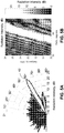
- FIG. 5A shows the measured realized gain 42 of the radiation pattern of the DAISA 30 shown in FIG. 2 .
- FIG. 5B shows the realized gain as a function of angle and frequency for the DAISA 30.
- FIG. 6A shows a 60cm x 38cm DAISA 50 designed to operate at 12 GHz and radiating predominantly towards 60 degrees off normal.
- FIG. 6B shows the measured realized gain 54 for the DAISA 50.
- a dielectric artificial impedance surface antenna (DAISA) in accordance with the present disclosure may be fabricated by forming a dielectric material into a shape to form a modulated impedance surface, as shown in step 100 in FIG. 8 .
- a dielectric is formed having a varying thickness to provide a modulated impedance to a signal traversing the dielectric, the dielectric having a first surface and a second surface opposite the first surface.
- the shape of the dielectric material may be formed by milling, stereo-lithography or by stamping, which is particularly suited for mass production, as shown in step 102.
- the dielectric material 20 may be any non-conducting material such as plastic, including Lexan®, acrylic, Plexiglas®, and other forms of plastic.
- the dielectric material 20 may be transparent or may be colored.
- the DAISA may be formed to mount conformally on a curved surface or be planar.
- a conductive ground plane may be formed on either the first surface 12 or the second surface 14 of the DAISA by metallic coating, which may be sprayed or deposited. Once the DAISA is fabricated a surface wave feed may be attached to the feed point 16 of the DAISA 10.
Landscapes
- Physics & Mathematics (AREA)
- Optics & Photonics (AREA)
- Details Of Aerials (AREA)
- Aerials With Secondary Devices (AREA)
Claims (9)
- Dielektrische künstliche Impedanzoberflächenantenne (10), die folgendes umfasst:ein im Wesentlichen planares Dielektrikum (20) mit einer Dicke, wobei das Dielektrikum (20) in einer XY-Ebene positioniert ist;einen Speisepunkt (16), der sich bei x = 0, y = 0 auf der ersten Oberfläche (12) befindet;wobei das Dielektrikum (20) eine erste Oberfläche (12) im Wesentlichen entlang der XY-Ebene aufweist und eine zweite Oberfläche (14) entgegengesetzt zu der ersten Oberfläche und im Wesentlichen entlang der XY=Ebene;wobei die Dicke des Dielektrikums verändert wird, um eine modulierte Impedanz Zsw(x,y) an ein das Dielektrikum durchquerendes Signal bereitzustellen; wobei die Dicke des Dielektrikums zwischen der ersten Oberfläche (12) und der zweiten Oberfläche (14) abhängig von einer gewünschten Frequenz und einem Strahlungswinkel der dielektrischen künstlichen Impedanzoberflächenantenne (10) moduliert wird;wobeidie modulierte Impedanz Zsw(x,y) ist und mit
 x eine Dimension der XY-Ebene ist;y eine andere Dimension der XY-Ebene ist,X eine durchschnittliche Impedanz ist;M eine maximale Oberflächenwellenimpedanzmodulation ist;f0 die Strahlungssollfrequenz ist;
 c eine Lichtgeschwindigkeit ist;r ein radialer Abstand von einem Speisepunkt (16) bei x=0, y=0 zu den Koordinaten von x, y ist; undθ0 der Strahlungssollwinkel ist.
 - Dielektrische künstliche Impedanzoberflächenantenne (10) nach Anspruch 1, wobei das Dielektrikum (20) ein nicht-leitendes Material, Kunststoff oder Acryl umfasst.
- Dielektrische künstliche Impedanzoberflächenantenne nach Anspruch 1, wobei das Dielektrikum (20) transparent oder gefärbt ist.
- Dielektrische künstliche Impedanzoberflächenantenne (10) nach Anspruch 1, wobei diese ferner eine leitende Bodenebene auf der ersten Oberfläche (12) oder auf der zweiten Oberfläche (14) umfasst.
- Dielektrische künstliche Impedanzoberflächenantenne (10) nach Anspruch 1, wobei diese ferner folgendes umfasst:eine Oberflächenwellenspeisung, die mit dem Speisepunkt (16) gekoppelt ist; wobei die Oberflächenwellenspeisung eine Mikrostreifenleitung (60), einen Wellenleiter (62), ein Mikrowellenhorn oder einen Dipol umfasst.
- Verfahren zur Herstellung einer dielektrischen künstlichen Impedanzoberflächenantenne (10), wobei das Verfahren folgendes umfasst:Bilden eines im Wesentlichen planaren Dielektrikums (20) mit einer Dicke, wobei das Dielektrikum (20) in einer XY-Ebene positioniert ist; wobei das Dielektrikum (20) eine erste Oberfläche im Wesentlichen entlang der XY-Ebene aufweist und eine zweite Oberfläche (14) entgegengesetzt zu der ersten Oberfläche (12) und im Wesentlichen entlang der XY-Ebene; undBereitstellen eines Speisepunkts (16), der sich bei x=0, y=0 auf der ersten Oberfläche (12) befindet;wobei das Verfahren ferner folgendes umfasst:Verändern der Dicke des Dielektrikums, um eine modulierte Impedanz Zsw(x,y) an ein das Dielektrikum durchquerendes Signal bereitzustellen; wobei die Dicke des Dielektrikums zwischen der ersten Oberfläche (12) und der zweiten Oberfläche (14) abhängig von einer gewünschten Frequenz und einem Strahlungswinkel der dielektrischen künstlichen Impedanzoberflächenantenne (10) moduliert wird;wobeidie modulierte Impedanz Zsw(x,y) ist und mit
 x eine Dimension der XY-Ebene ist;y eine andere Dimension der XY-Ebene ist,X eine durchschnittliche Impedanz ist;M eine maximale Oberflächenwellenimpedanzmodulation ist;f0 die Strahlungssollfrequenz ist;
 c eine Lichtgeschwindigkeit ist;rein radialer Abstand von einem Speisepunkt (16) bei x=0, y=0 zu den Koordinaten von x, y ist; undθ0 der Strahlungssollwinkel ist.
 - Verfahren nach Anspruch 6, wobei der Schritt des Bildens des Dielektrikums (20) Stanzen, Fräsen oder Stereolithographie umfasst.
- Verfahren nach Anspruch 6, wobei dieses ferner das Bilden einer leitenden Bodenebene auf der ersten Oberfläche (12) umfasst,
- Verfahren nach Anspruch 6, wobei dieses ferner folgendes umfasst:Bereitstellen einer Oberflächenwellenspeisung mit einer Mikrostreifenleitung (60), einem Wellenleiter (62), einem Mikrowellenhorn oder einem Dipol.
Applications Claiming Priority (2)
| Application Number | Priority Date | Filing Date | Title |
|---|---|---|---|
| US13/427,682 US8830129B2 (en) | 2012-03-22 | 2012-03-22 | Dielectric artificial impedance surface antenna |
| PCT/US2013/031079 WO2013142216A1 (en) | 2012-03-22 | 2013-03-13 | Dielectric artificial impedance surface antenna |
Publications (3)
| Publication Number | Publication Date |
|---|---|
| EP2828930A1 EP2828930A1 (de) | 2015-01-28 |
| EP2828930A4 EP2828930A4 (de) | 2015-06-24 |
| EP2828930B1 true EP2828930B1 (de) | 2017-12-13 |
Family
ID=49211271
Family Applications (1)
| Application Number | Title | Priority Date | Filing Date |
|---|---|---|---|
| EP13763659.3A Active EP2828930B1 (de) | 2012-03-22 | 2013-03-13 | Dielektrische künstliche impedanzoberflächenantenne |
Country Status (4)
| Country | Link |
|---|---|
| US (1) | US8830129B2 (de) |
| EP (1) | EP2828930B1 (de) |
| CN (1) | CN104185925B (de) |
| WO (1) | WO2013142216A1 (de) |
Families Citing this family (6)
| Publication number | Priority date | Publication date | Assignee | Title |
|---|---|---|---|---|
| US9312602B2 (en) * | 2012-03-22 | 2016-04-12 | Hrl Laboratories, Llc | Circularly polarized scalar impedance artificial impedance surface antenna |
| US9954284B1 (en) * | 2013-06-28 | 2018-04-24 | Hrl Laboratories, Llc | Skylight antenna |
| US10312596B2 (en) * | 2013-01-17 | 2019-06-04 | Hrl Laboratories, Llc | Dual-polarization, circularly-polarized, surface-wave-waveguide, artificial-impedance-surface antenna |
| US9910144B2 (en) * | 2013-03-07 | 2018-03-06 | Cpg Technologies, Llc | Excitation and use of guided surface wave modes on lossy media |
| US10451985B2 (en) * | 2017-02-28 | 2019-10-22 | Canon Kabushiki Kaisha | Toner |
| CN106887691B (zh) * | 2017-04-28 | 2019-04-09 | 电子科技大学 | 互补地全息调制表面双波束高增益天线 |
Family Cites Families (10)
| Publication number | Priority date | Publication date | Assignee | Title |
|---|---|---|---|---|
| JP3006930B2 (ja) | 1991-08-21 | 2000-02-07 | 財団法人国際科学振興財団 | 斜め二層誘電体構成マイクロストリップアンテナ及びその製造方法 |
| JP3166043B2 (ja) | 1992-01-22 | 2001-05-14 | 松下電器産業株式会社 | マイクロストリップアンテナ |
| JP3280716B2 (ja) | 1992-09-29 | 2002-05-13 | 松下電器産業株式会社 | マイクロストリップアンテナ |
| JP3034415B2 (ja) | 1993-11-16 | 2000-04-17 | 三菱電機株式会社 | アンテナ装置 |
| KR100549165B1 (ko) | 2002-09-23 | 2006-02-02 | 강정진 | 유전체 두께의 변화에 따른 급전라인을 가지는 이중 공진형개구 결합 고이득 패치 안테나 |
| US7830310B1 (en) * | 2005-07-01 | 2010-11-09 | Hrl Laboratories, Llc | Artificial impedance structure |
| US7218281B2 (en) * | 2005-07-01 | 2007-05-15 | Hrl Laboratories, Llc | Artificial impedance structure |
| US20070159396A1 (en) * | 2006-01-06 | 2007-07-12 | Sievenpiper Daniel F | Antenna structures having adjustable radiation characteristics |
| US7911407B1 (en) * | 2008-06-12 | 2011-03-22 | Hrl Laboratories, Llc | Method for designing artificial surface impedance structures characterized by an impedance tensor with complex components |
| KR101075753B1 (ko) * | 2008-12-22 | 2011-10-24 | 삼성전자주식회사 | 안테나 장치 및 그 제조방법 |
-
2012
- 2012-03-22 US US13/427,682 patent/US8830129B2/en active Active
-
2013
- 2013-03-13 CN CN201380004106.2A patent/CN104185925B/zh active Active
- 2013-03-13 EP EP13763659.3A patent/EP2828930B1/de active Active
- 2013-03-13 WO PCT/US2013/031079 patent/WO2013142216A1/en not_active Ceased
Non-Patent Citations (1)
| Title |
|---|
| None * |
Also Published As
| Publication number | Publication date |
|---|---|
| US8830129B2 (en) | 2014-09-09 |
| WO2013142216A1 (en) | 2013-09-26 |
| EP2828930A1 (de) | 2015-01-28 |
| CN104185925B (zh) | 2016-10-05 |
| US20130249737A1 (en) | 2013-09-26 |
| EP2828930A4 (de) | 2015-06-24 |
| CN104185925A (zh) | 2014-12-03 |
Similar Documents
| Publication | Publication Date | Title |
|---|---|---|
| Kanth et al. | EM design and analysis of frequency selective surface based on substrate-integrated waveguide technology for airborne radome application | |
| EP2828930B1 (de) | Dielektrische künstliche impedanzoberflächenantenne | |
| EP3017504B1 (de) | Elektronisch lenkbare antenne mit künstlicher impedanzoberfläche | |
| EP3522297B1 (de) | Weitwinkelabdeckungsantenne | |
| Wang et al. | Wideband Fabry-Perot resonator antenna with two complementary FSS layers | |
| US7429961B2 (en) | Method for fabricating antenna structures having adjustable radiation characteristics | |
| US7639207B2 (en) | Antenna structures having adjustable radiation characteristics | |
| US8730125B2 (en) | Low-cost high-gain planar antenna using a metallic mesh cap for millimeter-wave freqeuncy thereof | |
| US9444147B2 (en) | Ultra-wide-band (UWB) antenna assembly with at least one director and electromagnetic reflective subassembly and method | |
| Salonen et al. | WEBGA-wearable electromagnetic band-gap antenna | |
| Jindal et al. | Hybrid fractal antenna using meander and Minkowski curves for wireless applications | |
| Bauer et al. | A 79-GHz resonant laminated waveguide slotted array antenna using novel shaped slots in LTCC | |
| US9466887B2 (en) | Low cost, 2D, electronically-steerable, artificial-impedance-surface antenna | |
| JP2007081825A (ja) | 漏れ波アンテナ | |
| KR20150059392A (ko) | 스트립라인 급전 슬롯 배열 안테나 및 이의 제조 방법 | |
| EP3750212B1 (de) | Verschachtelte gruppenantenne mit betrieb bei mehreren frequenzen | |
| EP1661205A1 (de) | Strahlungssteuerung mit reaktiven elementen auf einer dielektrischen oberfläche | |
| JP7425868B2 (ja) | 電磁バンドギャップ構造物 | |
| US20190081409A1 (en) | Method and apparatus for a passive radiating and feed structure | |
| Tiwari et al. | Design of a Compact Antenna using Particle Swarm Optimization for the Entire Milli-meter Wave Range. | |
| CN114597641B (zh) | 一种基于函数逼近理论的扇形波束天线单元 | |
| Cong et al. | The conical conformal MEMS quasi-end-fire array antenna | |
| CN110120582B (zh) | 天线装置 | |
| Nissanov et al. | High directivity microstrip antenna with stopband and passband frequency selective surfaces for 6G at low-THz | |
| Arya | Reflectarray Antenna Designs |
Legal Events
| Date | Code | Title | Description |
|---|---|---|---|
| PUAI | Public reference made under article 153(3) epc to a published international application that has entered the european phase |
Free format text: ORIGINAL CODE: 0009012 |
|
| 17P | Request for examination filed |
Effective date: 20140702 |
|
| AK | Designated contracting states |
Kind code of ref document: A1 Designated state(s): AL AT BE BG CH CY CZ DE DK EE ES FI FR GB GR HR HU IE IS IT LI LT LU LV MC MK MT NL NO PL PT RO RS SE SI SK SM TR |
|
| AX | Request for extension of the european patent |
Extension state: BA ME |
|
| REG | Reference to a national code |
Ref country code: DE Ref legal event code: R079 Ref document number: 602013030804 Country of ref document: DE Free format text: PREVIOUS MAIN CLASS: H01Q0001380000 Ipc: H01Q0013280000 |
|
| RA4 | Supplementary search report drawn up and despatched (corrected) |
Effective date: 20150528 |
|
| RIC1 | Information provided on ipc code assigned before grant |
Ipc: H01Q 15/00 20060101ALI20150521BHEP Ipc: H01Q 13/28 20060101AFI20150521BHEP |
|
| DAX | Request for extension of the european patent (deleted) | ||
| 17Q | First examination report despatched |
Effective date: 20160426 |
|
| GRAP | Despatch of communication of intention to grant a patent |
Free format text: ORIGINAL CODE: EPIDOSNIGR1 |
|
| INTG | Intention to grant announced |
Effective date: 20170804 |
|
| GRAS | Grant fee paid |
Free format text: ORIGINAL CODE: EPIDOSNIGR3 |
|
| GRAA | (expected) grant |
Free format text: ORIGINAL CODE: 0009210 |
|
| AK | Designated contracting states |
Kind code of ref document: B1 Designated state(s): AL AT BE BG CH CY CZ DE DK EE ES FI FR GB GR HR HU IE IS IT LI LT LU LV MC MK MT NL NO PL PT RO RS SE SI SK SM TR |
|
| REG | Reference to a national code |
Ref country code: GB Ref legal event code: FG4D |
|
| REG | Reference to a national code |
Ref country code: AT Ref legal event code: REF Ref document number: 955207 Country of ref document: AT Kind code of ref document: T Effective date: 20171215 Ref country code: CH Ref legal event code: EP |
|
| REG | Reference to a national code |
Ref country code: IE Ref legal event code: FG4D |
|
| REG | Reference to a national code |
Ref country code: DE Ref legal event code: R096 Ref document number: 602013030804 Country of ref document: DE |
|
| REG | Reference to a national code |
Ref country code: NL Ref legal event code: MP Effective date: 20171213 |
|
| REG | Reference to a national code |
Ref country code: LT Ref legal event code: MG4D |
|
| PG25 | Lapsed in a contracting state [announced via postgrant information from national office to epo] |
Ref country code: NO Free format text: LAPSE BECAUSE OF FAILURE TO SUBMIT A TRANSLATION OF THE DESCRIPTION OR TO PAY THE FEE WITHIN THE PRESCRIBED TIME-LIMIT Effective date: 20180313 Ref country code: SE Free format text: LAPSE BECAUSE OF FAILURE TO SUBMIT A TRANSLATION OF THE DESCRIPTION OR TO PAY THE FEE WITHIN THE PRESCRIBED TIME-LIMIT Effective date: 20171213 Ref country code: LT Free format text: LAPSE BECAUSE OF FAILURE TO SUBMIT A TRANSLATION OF THE DESCRIPTION OR TO PAY THE FEE WITHIN THE PRESCRIBED TIME-LIMIT Effective date: 20171213 Ref country code: FI Free format text: LAPSE BECAUSE OF FAILURE TO SUBMIT A TRANSLATION OF THE DESCRIPTION OR TO PAY THE FEE WITHIN THE PRESCRIBED TIME-LIMIT Effective date: 20171213 |
|
| REG | Reference to a national code |
Ref country code: AT Ref legal event code: MK05 Ref document number: 955207 Country of ref document: AT Kind code of ref document: T Effective date: 20171213 |
|
| PG25 | Lapsed in a contracting state [announced via postgrant information from national office to epo] |
Ref country code: GR Free format text: LAPSE BECAUSE OF FAILURE TO SUBMIT A TRANSLATION OF THE DESCRIPTION OR TO PAY THE FEE WITHIN THE PRESCRIBED TIME-LIMIT Effective date: 20180314 Ref country code: RS Free format text: LAPSE BECAUSE OF FAILURE TO SUBMIT A TRANSLATION OF THE DESCRIPTION OR TO PAY THE FEE WITHIN THE PRESCRIBED TIME-LIMIT Effective date: 20171213 Ref country code: HR Free format text: LAPSE BECAUSE OF FAILURE TO SUBMIT A TRANSLATION OF THE DESCRIPTION OR TO PAY THE FEE WITHIN THE PRESCRIBED TIME-LIMIT Effective date: 20171213 Ref country code: BG Free format text: LAPSE BECAUSE OF FAILURE TO SUBMIT A TRANSLATION OF THE DESCRIPTION OR TO PAY THE FEE WITHIN THE PRESCRIBED TIME-LIMIT Effective date: 20180313 Ref country code: LV Free format text: LAPSE BECAUSE OF FAILURE TO SUBMIT A TRANSLATION OF THE DESCRIPTION OR TO PAY THE FEE WITHIN THE PRESCRIBED TIME-LIMIT Effective date: 20171213 |
|
| PG25 | Lapsed in a contracting state [announced via postgrant information from national office to epo] |
Ref country code: NL Free format text: LAPSE BECAUSE OF FAILURE TO SUBMIT A TRANSLATION OF THE DESCRIPTION OR TO PAY THE FEE WITHIN THE PRESCRIBED TIME-LIMIT Effective date: 20171213 |
|
| PG25 | Lapsed in a contracting state [announced via postgrant information from national office to epo] |
Ref country code: CZ Free format text: LAPSE BECAUSE OF FAILURE TO SUBMIT A TRANSLATION OF THE DESCRIPTION OR TO PAY THE FEE WITHIN THE PRESCRIBED TIME-LIMIT Effective date: 20171213 Ref country code: CY Free format text: LAPSE BECAUSE OF FAILURE TO SUBMIT A TRANSLATION OF THE DESCRIPTION OR TO PAY THE FEE WITHIN THE PRESCRIBED TIME-LIMIT Effective date: 20171213 Ref country code: EE Free format text: LAPSE BECAUSE OF FAILURE TO SUBMIT A TRANSLATION OF THE DESCRIPTION OR TO PAY THE FEE WITHIN THE PRESCRIBED TIME-LIMIT Effective date: 20171213 Ref country code: ES Free format text: LAPSE BECAUSE OF FAILURE TO SUBMIT A TRANSLATION OF THE DESCRIPTION OR TO PAY THE FEE WITHIN THE PRESCRIBED TIME-LIMIT Effective date: 20171213 Ref country code: SK Free format text: LAPSE BECAUSE OF FAILURE TO SUBMIT A TRANSLATION OF THE DESCRIPTION OR TO PAY THE FEE WITHIN THE PRESCRIBED TIME-LIMIT Effective date: 20171213 |
|
| PG25 | Lapsed in a contracting state [announced via postgrant information from national office to epo] |
Ref country code: IS Free format text: LAPSE BECAUSE OF FAILURE TO SUBMIT A TRANSLATION OF THE DESCRIPTION OR TO PAY THE FEE WITHIN THE PRESCRIBED TIME-LIMIT Effective date: 20180413 Ref country code: IT Free format text: LAPSE BECAUSE OF FAILURE TO SUBMIT A TRANSLATION OF THE DESCRIPTION OR TO PAY THE FEE WITHIN THE PRESCRIBED TIME-LIMIT Effective date: 20171213 Ref country code: RO Free format text: LAPSE BECAUSE OF FAILURE TO SUBMIT A TRANSLATION OF THE DESCRIPTION OR TO PAY THE FEE WITHIN THE PRESCRIBED TIME-LIMIT Effective date: 20171213 Ref country code: SM Free format text: LAPSE BECAUSE OF FAILURE TO SUBMIT A TRANSLATION OF THE DESCRIPTION OR TO PAY THE FEE WITHIN THE PRESCRIBED TIME-LIMIT Effective date: 20171213 Ref country code: AT Free format text: LAPSE BECAUSE OF FAILURE TO SUBMIT A TRANSLATION OF THE DESCRIPTION OR TO PAY THE FEE WITHIN THE PRESCRIBED TIME-LIMIT Effective date: 20171213 Ref country code: PL Free format text: LAPSE BECAUSE OF FAILURE TO SUBMIT A TRANSLATION OF THE DESCRIPTION OR TO PAY THE FEE WITHIN THE PRESCRIBED TIME-LIMIT Effective date: 20171213 |
|
| REG | Reference to a national code |
Ref country code: DE Ref legal event code: R097 Ref document number: 602013030804 Country of ref document: DE |
|
| PLBE | No opposition filed within time limit |
Free format text: ORIGINAL CODE: 0009261 |
|
| STAA | Information on the status of an ep patent application or granted ep patent |
Free format text: STATUS: NO OPPOSITION FILED WITHIN TIME LIMIT |
|
| REG | Reference to a national code |
Ref country code: CH Ref legal event code: PL |
|
| 26N | No opposition filed |
Effective date: 20180914 |
|
| GBPC | Gb: european patent ceased through non-payment of renewal fee |
Effective date: 20180313 |
|
| PG25 | Lapsed in a contracting state [announced via postgrant information from national office to epo] |
Ref country code: MC Free format text: LAPSE BECAUSE OF FAILURE TO SUBMIT A TRANSLATION OF THE DESCRIPTION OR TO PAY THE FEE WITHIN THE PRESCRIBED TIME-LIMIT Effective date: 20171213 Ref country code: DK Free format text: LAPSE BECAUSE OF FAILURE TO SUBMIT A TRANSLATION OF THE DESCRIPTION OR TO PAY THE FEE WITHIN THE PRESCRIBED TIME-LIMIT Effective date: 20171213 |
|
| REG | Reference to a national code |
Ref country code: BE Ref legal event code: MM Effective date: 20180331 |
|
| REG | Reference to a national code |
Ref country code: IE Ref legal event code: MM4A |
|
| PG25 | Lapsed in a contracting state [announced via postgrant information from national office to epo] |
Ref country code: LU Free format text: LAPSE BECAUSE OF NON-PAYMENT OF DUE FEES Effective date: 20180313 |
|
| PG25 | Lapsed in a contracting state [announced via postgrant information from national office to epo] |
Ref country code: IE Free format text: LAPSE BECAUSE OF NON-PAYMENT OF DUE FEES Effective date: 20180313 |
|
| PG25 | Lapsed in a contracting state [announced via postgrant information from national office to epo] |
Ref country code: GB Free format text: LAPSE BECAUSE OF NON-PAYMENT OF DUE FEES Effective date: 20180313 Ref country code: SI Free format text: LAPSE BECAUSE OF FAILURE TO SUBMIT A TRANSLATION OF THE DESCRIPTION OR TO PAY THE FEE WITHIN THE PRESCRIBED TIME-LIMIT Effective date: 20171213 Ref country code: CH Free format text: LAPSE BECAUSE OF NON-PAYMENT OF DUE FEES Effective date: 20180331 Ref country code: LI Free format text: LAPSE BECAUSE OF NON-PAYMENT OF DUE FEES Effective date: 20180331 Ref country code: BE Free format text: LAPSE BECAUSE OF NON-PAYMENT OF DUE FEES Effective date: 20180331 |
|
| PG25 | Lapsed in a contracting state [announced via postgrant information from national office to epo] |
Ref country code: FR Free format text: LAPSE BECAUSE OF NON-PAYMENT OF DUE FEES Effective date: 20180331 |
|
| PG25 | Lapsed in a contracting state [announced via postgrant information from national office to epo] |
Ref country code: MT Free format text: LAPSE BECAUSE OF NON-PAYMENT OF DUE FEES Effective date: 20180313 |
|
| PG25 | Lapsed in a contracting state [announced via postgrant information from national office to epo] |
Ref country code: TR Free format text: LAPSE BECAUSE OF FAILURE TO SUBMIT A TRANSLATION OF THE DESCRIPTION OR TO PAY THE FEE WITHIN THE PRESCRIBED TIME-LIMIT Effective date: 20171213 |
|
| PG25 | Lapsed in a contracting state [announced via postgrant information from national office to epo] |
Ref country code: HU Free format text: LAPSE BECAUSE OF FAILURE TO SUBMIT A TRANSLATION OF THE DESCRIPTION OR TO PAY THE FEE WITHIN THE PRESCRIBED TIME-LIMIT; INVALID AB INITIO Effective date: 20130313 Ref country code: PT Free format text: LAPSE BECAUSE OF FAILURE TO SUBMIT A TRANSLATION OF THE DESCRIPTION OR TO PAY THE FEE WITHIN THE PRESCRIBED TIME-LIMIT Effective date: 20171213 |
|
| PG25 | Lapsed in a contracting state [announced via postgrant information from national office to epo] |
Ref country code: MK Free format text: LAPSE BECAUSE OF NON-PAYMENT OF DUE FEES Effective date: 20171213 |
|
| PG25 | Lapsed in a contracting state [announced via postgrant information from national office to epo] |
Ref country code: AL Free format text: LAPSE BECAUSE OF FAILURE TO SUBMIT A TRANSLATION OF THE DESCRIPTION OR TO PAY THE FEE WITHIN THE PRESCRIBED TIME-LIMIT Effective date: 20171213 |
|
| P01 | Opt-out of the competence of the unified patent court (upc) registered |
Effective date: 20230523 |
|
| PGFP | Annual fee paid to national office [announced via postgrant information from national office to epo] |
Ref country code: DE Payment date: 20250327 Year of fee payment: 13 |