EP2827485A1 - Power feed device of inductive charging device - Google Patents
Power feed device of inductive charging device Download PDFInfo
- Publication number
- EP2827485A1 EP2827485A1 EP13760590.3A EP13760590A EP2827485A1 EP 2827485 A1 EP2827485 A1 EP 2827485A1 EP 13760590 A EP13760590 A EP 13760590A EP 2827485 A1 EP2827485 A1 EP 2827485A1
- Authority
- EP
- European Patent Office
- Prior art keywords
- power
- switching elements
- circuit
- factor
- power supply
- Prior art date
- Legal status (The legal status is an assumption and is not a legal conclusion. Google has not performed a legal analysis and makes no representation as to the accuracy of the status listed.)
- Granted
Links
- 230000001939 inductive effect Effects 0.000 title 1
- 239000003990 capacitor Substances 0.000 claims abstract description 66
- 230000006872 improvement Effects 0.000 claims abstract description 33
- 238000009499 grossing Methods 0.000 claims abstract description 32
- 238000010586 diagram Methods 0.000 description 19
- 238000005516 engineering process Methods 0.000 description 7
- 230000001965 increasing effect Effects 0.000 description 4
- 230000007246 mechanism Effects 0.000 description 3
- 230000009471 action Effects 0.000 description 2
- 238000001514 detection method Methods 0.000 description 2
- 230000009467 reduction Effects 0.000 description 2
- 230000003247 decreasing effect Effects 0.000 description 1
- 230000000694 effects Effects 0.000 description 1
- 230000005684 electric field Effects 0.000 description 1
- 230000002708 enhancing effect Effects 0.000 description 1
- 230000005669 field effect Effects 0.000 description 1
- 229920006395 saturated elastomer Polymers 0.000 description 1
- 239000004065 semiconductor Substances 0.000 description 1
- 230000001360 synchronised effect Effects 0.000 description 1
Images


Classifications
-
- H—ELECTRICITY
- H02—GENERATION; CONVERSION OR DISTRIBUTION OF ELECTRIC POWER
- H02M—APPARATUS FOR CONVERSION BETWEEN AC AND AC, BETWEEN AC AND DC, OR BETWEEN DC AND DC, AND FOR USE WITH MAINS OR SIMILAR POWER SUPPLY SYSTEMS; CONVERSION OF DC OR AC INPUT POWER INTO SURGE OUTPUT POWER; CONTROL OR REGULATION THEREOF
- H02M1/00—Details of apparatus for conversion
- H02M1/42—Circuits or arrangements for compensating for or adjusting power factor in converters or inverters
- H02M1/4208—Arrangements for improving power factor of AC input
- H02M1/4225—Arrangements for improving power factor of AC input using a non-isolated boost converter
-
- H—ELECTRICITY
- H02—GENERATION; CONVERSION OR DISTRIBUTION OF ELECTRIC POWER
- H02J—CIRCUIT ARRANGEMENTS OR SYSTEMS FOR SUPPLYING OR DISTRIBUTING ELECTRIC POWER; SYSTEMS FOR STORING ELECTRIC ENERGY
- H02J50/00—Circuit arrangements or systems for wireless supply or distribution of electric power
- H02J50/10—Circuit arrangements or systems for wireless supply or distribution of electric power using inductive coupling
- H02J50/12—Circuit arrangements or systems for wireless supply or distribution of electric power using inductive coupling of the resonant type
-
- H—ELECTRICITY
- H02—GENERATION; CONVERSION OR DISTRIBUTION OF ELECTRIC POWER
- H02J—CIRCUIT ARRANGEMENTS OR SYSTEMS FOR SUPPLYING OR DISTRIBUTING ELECTRIC POWER; SYSTEMS FOR STORING ELECTRIC ENERGY
- H02J50/00—Circuit arrangements or systems for wireless supply or distribution of electric power
- H02J50/80—Circuit arrangements or systems for wireless supply or distribution of electric power involving the exchange of data, concerning supply or distribution of electric power, between transmitting devices and receiving devices
-
- H—ELECTRICITY
- H02—GENERATION; CONVERSION OR DISTRIBUTION OF ELECTRIC POWER
- H02J—CIRCUIT ARRANGEMENTS OR SYSTEMS FOR SUPPLYING OR DISTRIBUTING ELECTRIC POWER; SYSTEMS FOR STORING ELECTRIC ENERGY
- H02J7/00—Circuit arrangements for charging or depolarising batteries or for supplying loads from batteries
- H02J7/00032—Circuit arrangements for charging or depolarising batteries or for supplying loads from batteries characterised by data exchange
- H02J7/00034—Charger exchanging data with an electronic device, i.e. telephone, whose internal battery is under charge
-
- H—ELECTRICITY
- H02—GENERATION; CONVERSION OR DISTRIBUTION OF ELECTRIC POWER
- H02M—APPARATUS FOR CONVERSION BETWEEN AC AND AC, BETWEEN AC AND DC, OR BETWEEN DC AND DC, AND FOR USE WITH MAINS OR SIMILAR POWER SUPPLY SYSTEMS; CONVERSION OF DC OR AC INPUT POWER INTO SURGE OUTPUT POWER; CONTROL OR REGULATION THEREOF
- H02M1/00—Details of apparatus for conversion
- H02M1/14—Arrangements for reducing ripples from dc input or output
-
- H—ELECTRICITY
- H02—GENERATION; CONVERSION OR DISTRIBUTION OF ELECTRIC POWER
- H02M—APPARATUS FOR CONVERSION BETWEEN AC AND AC, BETWEEN AC AND DC, OR BETWEEN DC AND DC, AND FOR USE WITH MAINS OR SIMILAR POWER SUPPLY SYSTEMS; CONVERSION OF DC OR AC INPUT POWER INTO SURGE OUTPUT POWER; CONTROL OR REGULATION THEREOF
- H02M1/00—Details of apparatus for conversion
- H02M1/0067—Converter structures employing plural converter units, other than for parallel operation of the units on a single load
- H02M1/007—Plural converter units in cascade
-
- Y—GENERAL TAGGING OF NEW TECHNOLOGICAL DEVELOPMENTS; GENERAL TAGGING OF CROSS-SECTIONAL TECHNOLOGIES SPANNING OVER SEVERAL SECTIONS OF THE IPC; TECHNICAL SUBJECTS COVERED BY FORMER USPC CROSS-REFERENCE ART COLLECTIONS [XRACs] AND DIGESTS
- Y02—TECHNOLOGIES OR APPLICATIONS FOR MITIGATION OR ADAPTATION AGAINST CLIMATE CHANGE
- Y02B—CLIMATE CHANGE MITIGATION TECHNOLOGIES RELATED TO BUILDINGS, e.g. HOUSING, HOUSE APPLIANCES OR RELATED END-USER APPLICATIONS
- Y02B70/00—Technologies for an efficient end-user side electric power management and consumption
- Y02B70/10—Technologies improving the efficiency by using switched-mode power supplies [SMPS], i.e. efficient power electronics conversion e.g. power factor correction or reduction of losses in power supplies or efficient standby modes
Definitions
- the present disclosure relates to non-contact charging devices for charging secondary batteries mounted, for example, on electric propulsion vehicles (electric vehicles and hybrid electric vehicles) in a non-contact fashion.
- electric propulsion vehicles electric vehicles and hybrid electric vehicles
- the non-contact power transfer technology does not require any wires for connecting a power feeding device and a power receiving device, and users do not have to connect the devices, and do not have to worry about leakage and an electric shock in the event of rain.
- positional relationship between the power feeding device and the power receiving device is important for enhanced efficiency.
- a technology of providing a resonance part for resonating an AC signal in each of the power feeding device and the power receiving device has been proposed to reduce a constraint of the positional relationship between the power feeding device and the power receiving device (see, e.g., Patent Document 1).
- Patent Document 1 a harmonic content having the same frequency as a frequency of a commercial power supply is superimposed on power output from the power feeding device.
- a current or voltage ripple of the harmonic content occurs in the output of the power feeding device, and a ripple occurs also in an output of the power receiving device, i.e., an output current to a battery, etc.
- a system of connecting a power supply and an electric propulsion vehicle via wires has been used to charge the electric propulsion vehicle, etc.
- high-speed feedback control is available when the ripple is detected in the current output to the battery.
- the high-speed feedback control cannot easily be performed because the power receiving device is wirelessly notified that the ripple is detected in the output current.
- the voltage ripple of the smoothing capacitors can be reduced.
- the multiple column circuits (converters) are required, and parts count of the power feeding device increases. This increases size and cost of the power feeding device, and increases loss of power feed.
- the present disclosure is intended to provide a power feeding device of a non-contact charging device which can reduce the ripple in the output, can achieve reduction in size and cost, and can reduce loss of power feed as much as possible.
- the present disclosure provides a power feeding device of a non-contact charging device for feeding power to a power receiving device in a non-contact fashion.
- the power feeding device includes a power factor improvement circuit which converts an AC power supply to DC, and improves a power factor, a smoothing capacitor connected to an output end of the power factor improvement circuit, an inverter circuit which includes a plurality of switching elements, and generates an AC signal by switching each of the switching elements using a voltage of the smoothing capacitor as a power supply, a power feeding section which includes a resonant capacitor and a first inductor connected to an output end of the inverter circuit, and feeds power generated between the first inductor and a second inductor provided in the power receiving device to the power receiving device based on the AC signal, and a control circuit which modulates a duty factor of each of the switching elements of the inverter circuit in synchronization with the AC power supply when the power feeding section feeds the power
- the power feeding device of the non-contact charging device can reduce the ripple in the output, can achieve reduction in size and cost, and can reduce loss of power feed.
- the present disclosure is directed to a power feeding device of a non-contact charging device for feeding power to a power receiving device in a non-contact fashion.
- the power feeding device includes a power factor improvement circuit which converts an AC power supply to DC, and improves a power factor, a smoothing capacitor connected to an output end of the power factor improvement circuit, an inverter circuit which includes a plurality of switching elements, and generates an AC signal by switching each of the switching elements using a voltage of the smoothing capacitor as a power supply, a power feeding section which includes a resonant capacitor and a first inductor connected to an output end of the inverter circuit, and feeds power generated between the first inductor and a second inductor provided in the power receiving device to the power receiving device based on the AC signal, and a control circuit which modulates a duty factor of each of the switching elements of the inverter circuit in synchronization with the AC power supply when the power feeding section feeds the power to the power receiving device.
- the control circuit controls the plurality of
- the control circuit increases an amount of modulation of the duty factor of the plurality of switching elements with increase in input from the AC power supply to the power feeding device.
- the control circuit modulates the duty factor in a substantially sinusoidal wave pattern at a frequency twice a frequency of the AC power supply.
- an output ripple of the power feeding device can be reduced not under feedback control which requires high detection accuracy, but under feedforward control.
- the ripple in the output of the power receiving device can be reduced, and the power feeding device no longer requires parts for detecting an output of the first inductor, or parts for detecting a voltage of the smoothing capacitor.
- parts count of the power feeding device is reduced, and the power feeding device can be reduced in size and cost.
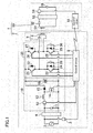
- FIG. 1 is a circuit diagram of a non-contact charging device of a first embodiment.
- a non-contact charging device 1 includes a power feeding device 2 located at a parking lot, for example, and a power receiving device 50 mounted on an electric propulsion vehicle, for example.
- the power feeding device 2 includes a commercial power supply 3, a first rectifier circuit 4, a synchronizing signal generator 5, a control circuit 6 for the power feeding device 2 (hereinafter merely referred to as a "control circuit 6"), a power feeding section 9, a power factor improvement circuit 10, and an inverter circuit 20.
- the power receiving device 50 includes a second inductor 51, a second resonant capacitor 52, a second rectifier circuit 53, a load (e.g., a battery) 18, a power reception detector 54, and a control circuit 55 for the power receiving device 50 (hereinafter merely referred to as a "control circuit 55").
- a control circuit 55 for the power receiving device 50 (hereinafter merely referred to as a "control circuit 55").
- the power factor improvement circuit 10 improves a power factor of the commercial power supply 3.
- the power factor improvement circuit 10 includes a bypass capacitor 11, an input detector 12, a choke coil 13, a first switching element 14 (a MOSFET: metal-oxide-semiconductor field-effect transistor in this embodiment), a first diode 15, and a smoothing capacitor (an electrolytic capacitor) 16.
- the commercial power supply 3 is a 200V commercial power supply which is a low-frequency AC power supply, for example, and is connected to an input end of the first rectifier circuit 4 including a bridge diode and an input filter.
- a high-side terminal of the bypass capacitor 11 and the input detector 12 are connected to a high-side (positive) output terminal of the first rectifier circuit 4.
- An output terminal of the input detector 12 is connected to an input terminal of the choke coil 13.
- a high-side terminal (drain) of the first switching element 14 is connected to a line connecting an output terminal of the choke coil 13 and an anode of the first diode 15.
- a low-side terminal of the bypass capacitor 11, a low-side terminal (source) of the first switching element 14, and a low-side terminal of the smoothing capacitor 16 are connected to a low-side (negative) output terminal of the first rectifier circuit 4.
- a high-side terminal of the smoothing capacitor 16 is connected to a cathode of the first diode 15.
- An output voltage of the first rectifier circuit 4 is input as a DC power supply to the power factor improvement circuit 10 constituted as described above.
- the bypass capacitor 11 reduces fluctuations of the output voltage of the first rectifier circuit 4.
- the output voltage of the first rectifier circuit 4 is then increased to an arbitrary voltage which is a DC voltage higher than a peak value of the output voltage by on-off action of the first switching element 14 and the choke coil 13.
- the increased voltage is fed to both ends of the smoothing capacitor 16, and is smoothed.
- the MOSFET which allows high-speed switching is used as the first switching element 14 to operate the power factor improvement circuit 10 at high frequency, thereby enhancing the effect of power factor improvement.
- a diode may be connected to the MOSFET in a reverse direction, but the diode is not shown in the figure because fundamental operation of the present embodiment is not affected even if the diode is not connected.
- An output voltage of the smoothing capacitor 16 is fed to input terminals of the inverter circuit 20.
- the input terminals of the inverter circuit 20 are connected to output terminals of the power factor improvement circuit 10, i.e., both ends of the smoothing capacitor 16.
- the power factor improvement circuit 10 i.e., both ends of the smoothing capacitor 16.
- serially-connected second and third switching elements 21 and 23 and serially-connected fourth and fifth switching elements 26 and 28 are connected in parallel.
- Second and third diodes 22 and 24 are connected in antiparallel to the second and third switching elements 21 and 23, respectively. Specifically, high-side terminals (collectors) of the switching elements and cathodes of the diodes are connected.
- a snubber capacitor 25 is connected in parallel to the third switching element 23. The snubber capacitor 25 may be connected in parallel to the second switching element 21.
- fourth and fifth diodes 27 and 29 are connected in antiparallel to fourth and fifth switching elements 26 and 28, respectively.
- high-side terminals (collectors) of the switching elements are connected to cathodes of the diodes.
- a snubber capacitor 30 is connected in parallel to the fifth switching element 28.
- the snubber capacitor 30 may be connected in parallel to the fourth switching element 26.
- the power feeding section 9 is connected to a line connecting the second switching element 21 and the third switching element 23, and a line connecting the fourth switching element 26 and the fifth switching element 28.
- the inverter circuit 20 generates an AC signal by switching the second to fifth switching elements 21, 23, 26, and 28, and outputs the signal to the power feeding section 9.
- the power feeding section 9 can be constituted of a first resonant capacitor 7 and a first inductor 8 connected in series.
- the second inductor 51 is arranged to face the first inductor 8 when the electric propulsion vehicle has moved, for example.
- the power feeding section 9 can feed power generated between the first and second inductors 8 and 51 to the power receiving device 50 based on the AC signal output by the inverter circuit 20.
- the second resonant capacitor 52 is connected to a high-side terminal of the second inductor 51.
- the second rectifier circuit 53 including a smoothing filter is connected between a low-side terminal of the second inductor 51 and the second resonant capacitor 52.
- the power reception detector 54 is connected to a high-side terminal of the second rectifier circuit 53, and a load, e.g., the battery 18, is connected between the power reception detector 54 and a low-side terminal of the second rectifier circuit 53.
- FIG. 2 is a circuit diagram illustrating an example of the input detector shown in FIG. 1 .
- the input detector 12 is constituted of a current detector 31, a voltage detector 32, and a power operation part 33.
- the power operation part 33 is connected to the control circuit 6.
- the input power can be estimated from one of the current or the voltage
- one of the current detector 31 or the voltage detector 32 may be provided.
- FIG. 3 is a circuit diagram illustrating an example of the synchronizing signal generator shown in FIG. 1 .
- the synchronizing signal generator 5 is constituted of a plurality of resistance elements 34, 35, 36, and 37, and a transistor 38 as shown in FIG. 3 .
- the synchronizing signal generator 5 generates a signal having a frequency synchronized with a frequency of the commercial power supply 3, and outputs the generated signal to the control circuit 6.
- Vdd indicates a control voltage of the control circuit 6.
- the control circuit 6 synchronizes with the synchronizing signal to perform modulation on the inverter circuit 20.
- the synchronizing signal contains delay time due to on/off action of the transistor 38, and the delay time is ⁇ relative to a cycle of the commercial power supply 3.
- the power reception detector 54 may be configured in the same manner as the input detector 12.
- the control circuit 6 wirelessly receives a power command value indicating a power value to be fed to the power receiving device 50 from the control circuit 55.
- the control circuit 6 compares power based on the input current detected by the input detector 12 and the received power command value, and controls the second and third switching elements 21 and 23 and the fourth and fifth switching elements 26 and 28 of the inverter circuit 20, and the first switching element 14 of the power factor improvement circuit 10 so that power corresponding to the power command value is output.
- an exclusive control IC may be used to control the first switching element 14.
- the control circuit 55 determines the power command value based on a remaining voltage of the battery 18 detected by the power reception detector 54, and wirelessly sends the power command value to the control circuit 6.
- the control circuit 55 changes the power command value to be sent to the control circuit 6 based on received power detected by the power reception detector 54 so that overcurrent or overvoltage is not applied to the battery 18.
- a battery for electric propulsion vehicles is used as the battery 18 of the present embodiment.
- a voltage not lower than the remaining voltage of the battery is fed.
- a charging current flows abruptly. This indicates that impedance of a load as seen from the power feeding device greatly varies depending on the remaining voltage of the battery 18 and the fed voltage.
- FIGS. 4A-4H A working mechanism of the non-contact charging device 1 configured as described above will be described below.
- FIGS. 4A-4H voltage waveforms and current waveforms of sections of a power transfer system of Patent Document 1 will be described with reference to FIGS. 4A-4H .
- the non-contact charging device 1 of the present embodiment and the power transfer system of Patent Document 1 have different configurations.
- items "output voltage of first rectifier circuit 4", "output voltage of power factor improvement circuit 10,” etc. are described to compare the non-contact charging device 1 of the present embodiment and the power transfer system of Patent Document 1, and to indicate the output voltage etc., of the corresponding parts of the power transfer system of Patent Document 1.
- FIG. 4A is a diagram showing a waveform of an AC voltage of the commercial power supply 3
- FIG. 4B is a diagram showing a waveform of an output voltage of a DC power supply, i.e., a waveform of an output voltage of the first rectifier circuit 4.
- the voltage is input to the power factor improvement circuit 10, increased, and then output to the smoothing capacitor 16.
- FIG. 4C is a diagram showing a waveform of a voltage applied to the smoothing capacitor 16, i.e., a waveform of an output voltage of the power factor improvement circuit 10 and a waveform of an input voltage of the inverter circuit 20.
- FIG. 4D is a diagram showing a waveform of a high-frequency current generated at the first inductor 8
- FIG. 4E is a diagram showing a waveform of power fed from the power feeding device 2 to the power receiving device 50.
- FIG. 4F is a diagram showing a waveform of an output current of the second rectifier circuit 53, i.e., a waveform of an input current of the load 18.
- FIGS. 4G and 4H are diagrams showing a duty factor (duty ratio) and an operating frequency of the inverter circuit 20, respectively.
- FIGS. 5A-5I show voltage waveforms, current waveforms, etc., of sections of the non-contact charging device of the present embodiment, and FIGS. 5A-5H correspond to FIGS. 4A-4H , respectively.
- the duty factor (duty ratio) and the operation frequency of the inverter circuit 20 are both fixed as shown in FIGS. 4G and 4H .
- the output of the commercial power supply 3 shown in FIG. 5A is full-wave rectified by the first rectifier circuit 4, and a DC power supply as depicted by the voltage waveform in FIG. 5B is formed.
- the DC power supply is fed between input terminals of the power factor improvement circuit 10.
- the power factor improvement circuit 10 when an instantaneous value of a voltage of the DC power supply is smaller than the voltage of the smoothing capacitor 16, the first diode 15 in the power factor improvement circuit 10 and the bridge diode of the first rectifier circuit 4 are not turned on, an input current waveform is distorted, and the power factor is significantly decreased.
- the control circuit 6 turns the first switching element 14 on/off to improve the power factor of the power factor improvement circuit 10.
- the power factor improvement circuit 10 has the functions of improving the power factor, and increasing the voltage.
- the voltage of the smoothing capacitor 16 has a peak value higher than a peak value of the commercial power supply 3, i.e., a peak value of the input voltage of the power factor improvement circuit 10, which is a peak value of the DC power supply, and the voltage is fed to the inverter circuit 20 through the smoothing capacitor 16.
- a voltage ripple having a frequency twice the frequency of the commercial power supply 3 relative to a target output voltage Vpfc of the power factor improvement circuit 10 occurs as shown in FIG. 5C .
- the power transfer system of Patent Document 1 and the non-contact charging device 1 of the present embodiment do not have significant difference in waveform of the AC voltage of the commercial power supply 3, waveform of the output voltage of the first rectifier circuit 4, and waveform of the output voltage of the power factor improvement circuit 10.
- a smoothed DC voltage output to the both ends of the smoothing capacitor 16 connected to output ends of the power factor improvement circuit 10 is fed to the inverter circuit 20 (see FIG. 5C ).
- a high-frequency current of a predetermined frequency is generated in the first resonant capacitor 7 and the first inductor 8 as shown in FIG. 5D by on/off switching of the second and third switching elements 21 and 23, and on/off switching of the fourth and fifth switching elements 26 and 28.
- the on/off control of the second and third switching elements 21 and 23, and the on/off control of the fourth and fifth switching elements 26 and 28 are performed by applying an on signal or an off signal to gates of the second to fifth switching elements 21, 23, 26, and 28 from the control circuit 6.
- FIGS. 6A-6F are enlarged diagrams of operating waveforms of the inverter circuit when input power is high
- FIGS. 7A-7F are enlarged diagrams of operating waveforms of the inverter circuit when input power is low.
- FIGS. 6A-6F and FIGS. 7A-7F show the current flowing through the second and fifth switching elements 21 and 28, and the current flowing through the second and fifth diodes 22 and 29, respectively.
- FIGS. 6B and 7B show the current flowing through the third and fourth switching elements 23 and 26, and the current flowing through the third and fourth diodes 24 and 27, respectively.
- FIGS. 6C and 7C show the voltage of the second and fifth switching elements 21 and 28.
- FIGS. 6D and 7D show a gate voltage of the second and fifth switching elements 21 and 28.
- FIGS. 6E and 7E show a gate voltage of the third and fourth switching elements 23 and 26.
- FIGS. 6F and 7F show a current IL1 flowing through the first inductor 8.
- the current flows through the second and third switching elements 21 and 28, and the second and fifth diodes 22 and 29 in a period Ton in a switching cycle.
- the current flows through the third and fourth switching elements 23 and 26, and the third and fourth diodes 24 and 27.
- Td dead time
- the serially-connected second and third switching elements 21 and 23 are exclusively energized.
- the fourth and fifth switching elements 26 and 28 are exclusively energized by a driving signal which is phase-shifted from a driving signal of the second and third switching elements 21 and 23.
- the second switching element 21 and the fifth switching element 28 are on/off controlled in synchronization.
- the third switching element 23 and the fourth switching element 26 are off.
- the third switching element 23 and the fourth switching element 26 are on.
- the third switching element 23 and the fourth switching element 26 are on/off controlled in synchronization.
- the dead time Td is provided so that the second switching element 21 and the third switching element 23 are not simultaneously turned on, the fourth switching element 26 and the fifth switching element 28 are not simultaneously turned on, and a period in which the second and fourth switching elements 21 and 26 are on does not coincide with a period in which the third and fifth switching elements 23 and 28 are on.
- the second and fifth switching elements 21 and 28 are turned off from an on state.
- the snubber capacitor 25 is slowly discharged.
- the second and fifth switching elements 21 and 28 are turned off by zero voltage switching (ZVS).
- ZVS zero voltage switching
- the snubber capacitor 30 is charged.
- the third and fourth diodes 24 and 27 are turned on.
- the third and fourth switching elements 23 and 26 are turned off from the on state.
- the snubber capacitor 30 is slowly discharged.
- the third and fourth switching elements 23 and 26 are turned off by ZVS.
- the snubber capacitor 25 is charged.
- the second and fifth diodes 22 and 29 are turned on. While the second and fifth diodes 22 and 29 are on, an on signal is sent to gates of the second and fifth switching elements 21 and 28, and the direction of the resonance current of the first inductor 8 is reversed after a predetermined time, thereby turning the fifth diode 29 off.
- the current is commutated to the second and fifth switching elements 21 and 28, and the second and fifth switching elements 21 and 28 are turned on by ZVS and ZCS.
- the inverter circuit 20 is operated as described above.
- a dead time Td of about 2 ⁇ s is set so as not to establish a short circuit in the smoothing capacitor 16, and the second and fifth switching elements 21 and 28, and the third and fourth switching elements 23 and 26 are alternately turned on/off.
- the drive frequencies (operation frequencies) of the second to fifth switching elements 21, 23, 26, and 28 are kept constant as shown in FIG. 5H , and a duty factor (duty ratio) is controlled as shown in FIG. 5G to control the high-frequency power.
- the term "duty factor" is defined as a ratio of the period when the second and fifth switching elements 21 and 28 (or the third and fourth switching elements 23 and 26) are on to a period of time required for a single on/off cycle of the second and fifth switching elements 21 and 28 (or the third and fourth switching elements 23 and 26) as shown in FIGS. 6A-6F and 7A-7F .
- FIGS. 4A-4H when the frequency of the commercial power supply 3 is 60 Hz, an input voltage containing a voltage ripple and having a frequency of 120 Hz, which is twice the frequency of the commercial power supply 3, is applied to the inverter circuit 20 as shown in FIG. 4C .
- a current ripple occurs in the current of the first inductor 8. Therefore, fed power (transferred power) fluctuates as shown in FIG. 4E , and as a result, a current ripple of 120 Hz occurs in the input current of the load 18 as shown in FIG. 4F .
- the frequency of the commercial power supply 3 is 50 Hz. In this case, a current ripple of 100 Hz occurs in the input current of the load 18.
- the duty factor (duty ratio) of the second to fifth switching elements 21, 23, 26, and 28 is modulated by the control circuit 6 in synchronization with the output of the commercial power supply 3 at a ⁇ duty factor (see FIGS. 5A-5I and FIG. 8 ) which is an amount of modulation determined based on the input current from the commercial power supply 3 detected by the input detector 12.
- the duty factor (duty ratio) is modulated so that an increment of the duty factor ( ⁇ duty factor+) is not smaller than a decrement of the duty factor ( ⁇ duty factor-).
- the modulation in this way can keep the current flowing through the first inductor 8 and the power fed by the power feeding device substantially constant as shown in FIGS. 5D and 5E . Further, switching loss of the second to fifth switching elements 21, 23, 26, and 28 of the inverter circuit 20 can be reduced.
- the inverter circuit 20 is operated to increase the switching loss.
- the duty factor (duty ratio) and the input power show a relationship as shown in FIG. 9 in which the input power is saturated when the duty factor is 50%.
- the second to fifth switching elements 21, 23, 26, and 28 are operated at a duty factor in a range where an input power characteristic curve relative to the duty factor is substantially linear (range B), e.g., at a duty factor a shown in FIG. 9 . This can facilitate the control.
- the duty factors of the second to fifth switching elements 21, 23, 26, and 28 are modulated in such a manner that the ⁇ duty factor+ is not smaller than the ⁇ duty factor- with reference to a duty factor b shown in FIG. 9 , i.e., the increment of the duty factor and the decrement of the duty factor are not equal.
- the increment and the decrement of the power can be matched, and the switching elements can be operated to reduce the switching loss.
- current ripple and voltage ripple which occur in the output of the power feeding device 2 at a frequency twice the frequency of the commercial power supply 3 can be reduced. Since the ⁇ duty factor+ and the ⁇ duty factor- shown in FIG. 8 may be constant irrespective of the frequency of the commercial power supply 3, the modulation can easily be performed.
- the voltage ripple of the smoothing capacitor 16 shown in FIG. 5C increases with the increase in input power.
- the control circuit 6 controls the inverter circuit 20 so that the ⁇ duty factor increases with the increase in input current as shown in FIG. 8 .
- the control circuit 6 stores information about a relationship between the input current and the ⁇ duty ratio as shown in FIG. 8 , and can perform feedforward control based on the input current.
- the control circuit 6 modulates the duty factor in synchronization with the output of the commercial power supply 3 based on the signal output by the synchronizing signal generator 5 shown in FIG. 5I .
- This modulation can cancel the voltage ripple of the smoothing capacitor 16 shown in FIG. 5C which occurs in synchronization with the commercial power supply 3.
- the current ripple which occurs in the output of the power receiving device 50 can precisely be reduced.
- the output of the synchronizing signal generator 5 contains delay time ⁇ shown in FIG. 5I relative to the cycle of the commercial power supply 3, and the control circuit 6 corrects the delay time ⁇ to perform the modulation.
- the delay time ⁇ can be fixed irrespective of the input power etc., and the delay time ⁇ can easily be corrected by the control circuit 6.
- the duty factor is set high when the input power is high as compared with the case where the input power is low (for example, the duty factor is 40-50% when the input power is high, and is 20%-30% when the input power is low).
- the control circuit 6 modulates the second to fifth switching elements 21, 23, 26, and 28 so that the duty factor is set low when the voltage is high, and is set high when the voltage is low (see FIG. 5G ).
- the current flowing through the first inductor 8 and the power fed to the power receiving device 50 can be kept substantially constant (see FIG. 5E ).
- the control circuit 55 determines command values of the charging current, the voltage, the power, etc., based on the remaining voltage of the battery detected by the power reception detector 54. Then, the control circuit 55 wirelessly sends the determined command value (e.g., the power command value described above) to the control circuit 6. In the charging operation, the control circuit 55 wirelessly sends information such as the charging current, the voltage, the power, etc., to the control circuit 6. Thus, the control circuit 6 controls the charging current, the voltage, the power, etc., to be fed to the power receiving device 50 based on the received information.
- the determined command value e.g., the power command value described above
- efficiency of power transfer between the first inductor 8 and the second inductor 51 can be enhanced by resonating the second inductor 51 and the second resonant capacitor 52.
- the second resonant capacitor 52 can cancel an impedance component derived from leakage inductance which is not magnetically coupled with the first inductor 8.
- impedance of a secondary part (the power receiving device) can be reduced, and as a result, the power transfer can be facilitated.
- the second resonant capacitor 52 may be omitted.
- control circuit 6 Upon receiving the power command value from the control circuit 55, the control circuit 6 performs the above-described operation to control the power factor improvement circuit 10 and the inverter circuit 20 so that the power command value corresponds with the detection result of the input detector 12.
- control circuit 6 is configured to control the second to fifth switching elements 21, 23, 26, and 28 based on the current value detected by the input detector 12.
- the amount of modulation may be determined based on the input power detected by the input detector 12.
- the inverter circuit 20 is controlled in such a manner that the increment of the duty factor is not smaller than the decrement of the duty factor.
- the inverter circuit 20 may be controlled in such a manner that the decrement of the duty factor is greater than the increment of the duty factor.
- the power feeding device of the non-contact charging device of the present disclosure can reduce superimposition of a current/voltage ripple of a harmonic content derived from a frequency of a commercial power supply on the output of the power feeding device, and can reduce parts count of the power feeding device.
- the power feeding device can be reduced in size or cost, and can reduce loss of power feed as much as possible. Therefore, the present disclosure is useful for, for example, power feeding to power receiving devices of electric propulsion vehicles.
Landscapes
- Engineering & Computer Science (AREA)
- Power Engineering (AREA)
- Computer Networks & Wireless Communication (AREA)
- Charge And Discharge Circuits For Batteries Or The Like (AREA)
- Rectifiers (AREA)
- Inverter Devices (AREA)
- Electric Propulsion And Braking For Vehicles (AREA)
- Dc-Dc Converters (AREA)
Abstract
Description
- The present disclosure relates to non-contact charging devices for charging secondary batteries mounted, for example, on electric propulsion vehicles (electric vehicles and hybrid electric vehicles) in a non-contact fashion.
- Technologies using a magnetic field, an electric field, a radio wave, etc., have been developed to achieve power transfer in a non-contact fashion. The non-contact power transfer technology does not require any wires for connecting a power feeding device and a power receiving device, and users do not have to connect the devices, and do not have to worry about leakage and an electric shock in the event of rain.
- In the non-contact power transfer, for example, positional relationship between the power feeding device and the power receiving device is important for enhanced efficiency. In this regard, a technology of providing a resonance part for resonating an AC signal in each of the power feeding device and the power receiving device has been proposed to reduce a constraint of the positional relationship between the power feeding device and the power receiving device (see, e.g., Patent Document 1).
- According to the technology taught by
Patent Document 1, a harmonic content having the same frequency as a frequency of a commercial power supply is superimposed on power output from the power feeding device. As a result, a current or voltage ripple of the harmonic content occurs in the output of the power feeding device, and a ripple occurs also in an output of the power receiving device, i.e., an output current to a battery, etc. - A system of connecting a power supply and an electric propulsion vehicle via wires has been used to charge the electric propulsion vehicle, etc. In the wired system, high-speed feedback control is available when the ripple is detected in the current output to the battery. In the non-contact charging system, however, the high-speed feedback control cannot easily be performed because the power receiving device is wirelessly notified that the ripple is detected in the output current.
- As a solution to the above problem, a technology has been proposed that three column circuits (converters) each comprising a serially-connected four stage circuit are connected in parallel to share a plurality of smoothing capacitors, and each of the column circuits is driven by shifting their phases by 2π/3(rad) (see, e.g., Patent Document 2). In this technology, the voltage ripple can be reduced by sharing a charge/discharge current to the plurality of smoothing capacitors among the column circuits.
-
- Patent Document 1: Japanese Unexamined Patent Publication No.
2009-296857 - Patent Document 2: Japanese Unexamined Patent Publication No.
2008-263715 - According to the disclosure of Patent Document 2, the voltage ripple of the smoothing capacitors can be reduced. However, the multiple column circuits (converters) are required, and parts count of the power feeding device increases. This increases size and cost of the power feeding device, and increases loss of power feed.
- In view of the foregoing, the present disclosure is intended to provide a power feeding device of a non-contact charging device which can reduce the ripple in the output, can achieve reduction in size and cost, and can reduce loss of power feed as much as possible.
- To achieve the above-described object, the present disclosure has proposed the following solution. Specifically, the present disclosure provides a power feeding device of a non-contact charging device for feeding power to a power receiving device in a non-contact fashion. The power feeding device includes a power factor improvement circuit which converts an AC power supply to DC, and improves a power factor, a smoothing capacitor connected to an output end of the power factor improvement circuit, an inverter circuit which includes a plurality of switching elements, and generates an AC signal by switching each of the switching elements using a voltage of the smoothing capacitor as a power supply, a power feeding section which includes a resonant capacitor and a first inductor connected to an output end of the inverter circuit, and feeds power generated between the first inductor and a second inductor provided in the power receiving device to the power receiving device based on the AC signal, and a control circuit which modulates a duty factor of each of the switching elements of the inverter circuit in synchronization with the AC power supply when the power feeding section feeds the power to the power receiving device. The control circuit controls the plurality of switching elements so that an increment of the modulated duty factor is not equal to a decrement of the modulated duty factor.
- According to the present disclosure, the power feeding device of the non-contact charging device can reduce the ripple in the output, can achieve reduction in size and cost, and can reduce loss of power feed.
-
- [
FIG. 1] FIG. 1 is a circuit diagram illustrating a non-contact charging device of a first embodiment. - [
FIG. 2] FIG. 2 is a circuit diagram illustrating an example of an input detector shown inFIG. 1 . - [
FIG. 3] FIG. 3 is a circuit diagram illustrating an example of a synchronizing signal generator shown inFIG. 1 . - [
FIG. 4] FIGS. 4A-4H are diagrams of waveforms obtained at sections of a conventional power transfer system for comparison with the non-contact charging device ofFIG. 1 . - [
FIG. 5] FIGS. 5A-5I are diagrams of waveforms obtained at sections of the non-contact charging device ofFIG. 1 when a duty factor of the inverter circuit shown inFIG. 1 is varied. - [
FIG. 6] FIGS. 6A-6F are enlarged diagrams of operating waveforms of the inverter circuit when input power is high. - [
FIG. 7] FIGS. 7A-7F are enlarged diagrams of operating waveforms of the inverter circuit when the input power is low. - [
FIG. 8] FIG. 8 is a graph showing a relationship between input current and Δduty factor of a feeding device shown inFIG. 1 . - [
FIG. 9] FIG. 9 is a graph showing a relationship between input power and duty factor of the feeding device shown inFIG. 1 . - The present disclosure is directed to a power feeding device of a non-contact charging device for feeding power to a power receiving device in a non-contact fashion. The power feeding device includes a power factor improvement circuit which converts an AC power supply to DC, and improves a power factor, a smoothing capacitor connected to an output end of the power factor improvement circuit, an inverter circuit which includes a plurality of switching elements, and generates an AC signal by switching each of the switching elements using a voltage of the smoothing capacitor as a power supply, a power feeding section which includes a resonant capacitor and a first inductor connected to an output end of the inverter circuit, and feeds power generated between the first inductor and a second inductor provided in the power receiving device to the power receiving device based on the AC signal, and a control circuit which modulates a duty factor of each of the switching elements of the inverter circuit in synchronization with the AC power supply when the power feeding section feeds the power to the power receiving device. The control circuit controls the plurality of switching elements so that an increment of the modulated duty factor is not equal to a decrement of the modulated duty factor.
- The control circuit increases an amount of modulation of the duty factor of the plurality of switching elements with increase in input from the AC power supply to the power feeding device.
- The control circuit modulates the duty factor in a substantially sinusoidal wave pattern at a frequency twice a frequency of the AC power supply.
- In this configuration, an output ripple of the power feeding device can be reduced not under feedback control which requires high detection accuracy, but under feedforward control. As a result, the ripple in the output of the power receiving device can be reduced, and the power feeding device no longer requires parts for detecting an output of the first inductor, or parts for detecting a voltage of the smoothing capacitor. Thus, parts count of the power feeding device is reduced, and the power feeding device can be reduced in size and cost.
- Embodiments of the present disclosure will be described below with reference to the drawings. The present disclosure is not limited by the embodiments.
-
FIG. 1 is a circuit diagram of a non-contact charging device of a first embodiment. As shown inFIG. 1 , anon-contact charging device 1 includes a power feeding device 2 located at a parking lot, for example, and apower receiving device 50 mounted on an electric propulsion vehicle, for example. The power feeding device 2 includes acommercial power supply 3, a first rectifier circuit 4, asynchronizing signal generator 5, acontrol circuit 6 for the power feeding device 2 (hereinafter merely referred to as a "control circuit 6"), apower feeding section 9, a powerfactor improvement circuit 10, and aninverter circuit 20. - The
power receiving device 50 includes asecond inductor 51, a secondresonant capacitor 52, asecond rectifier circuit 53, a load (e.g., a battery) 18, apower reception detector 54, and acontrol circuit 55 for the power receiving device 50 (hereinafter merely referred to as a "control circuit 55"). - Configurations of these circuit blocks will be described below.
- First, a configuration of the power
factor improvement circuit 10 will be described. The powerfactor improvement circuit 10 improves a power factor of thecommercial power supply 3. Specifically, the powerfactor improvement circuit 10 includes a bypass capacitor 11, aninput detector 12, achoke coil 13, a first switching element 14 (a MOSFET: metal-oxide-semiconductor field-effect transistor in this embodiment), afirst diode 15, and a smoothing capacitor (an electrolytic capacitor) 16. - The
commercial power supply 3 is a 200V commercial power supply which is a low-frequency AC power supply, for example, and is connected to an input end of the first rectifier circuit 4 including a bridge diode and an input filter. - A high-side terminal of the bypass capacitor 11 and the
input detector 12 are connected to a high-side (positive) output terminal of the first rectifier circuit 4. An output terminal of theinput detector 12 is connected to an input terminal of thechoke coil 13. - A high-side terminal (drain) of the
first switching element 14 is connected to a line connecting an output terminal of thechoke coil 13 and an anode of thefirst diode 15. A low-side terminal of the bypass capacitor 11, a low-side terminal (source) of thefirst switching element 14, and a low-side terminal of the smoothingcapacitor 16 are connected to a low-side (negative) output terminal of the first rectifier circuit 4. A high-side terminal of the smoothingcapacitor 16 is connected to a cathode of thefirst diode 15. - An output voltage of the first rectifier circuit 4 is input as a DC power supply to the power
factor improvement circuit 10 constituted as described above. First, the bypass capacitor 11 reduces fluctuations of the output voltage of the first rectifier circuit 4. The output voltage of the first rectifier circuit 4 is then increased to an arbitrary voltage which is a DC voltage higher than a peak value of the output voltage by on-off action of thefirst switching element 14 and thechoke coil 13. The increased voltage is fed to both ends of the smoothingcapacitor 16, and is smoothed. - In the present embodiment, the MOSFET which allows high-speed switching is used as the
first switching element 14 to operate the powerfactor improvement circuit 10 at high frequency, thereby enhancing the effect of power factor improvement. In this case, a diode may be connected to the MOSFET in a reverse direction, but the diode is not shown in the figure because fundamental operation of the present embodiment is not affected even if the diode is not connected. An output voltage of the smoothingcapacitor 16 is fed to input terminals of theinverter circuit 20. - The input terminals of the
inverter circuit 20 are connected to output terminals of the powerfactor improvement circuit 10, i.e., both ends of the smoothingcapacitor 16. To the both ends of the smoothingcapacitor 16, serially-connected second andthird switching elements fifth switching elements - Second and
third diodes third switching elements snubber capacitor 25 is connected in parallel to thethird switching element 23. Thesnubber capacitor 25 may be connected in parallel to thesecond switching element 21. - Likewise, fourth and
fifth diodes fifth switching elements snubber capacitor 30 is connected in parallel to thefifth switching element 28. Thesnubber capacitor 30 may be connected in parallel to thefourth switching element 26. - The
power feeding section 9 is connected to a line connecting thesecond switching element 21 and thethird switching element 23, and a line connecting thefourth switching element 26 and thefifth switching element 28. - The
inverter circuit 20 generates an AC signal by switching the second tofifth switching elements power feeding section 9. - The
power feeding section 9 can be constituted of a first resonant capacitor 7 and afirst inductor 8 connected in series. - The
second inductor 51 is arranged to face thefirst inductor 8 when the electric propulsion vehicle has moved, for example. Thus, thepower feeding section 9 can feed power generated between the first andsecond inductors power receiving device 50 based on the AC signal output by theinverter circuit 20. - The second
resonant capacitor 52 is connected to a high-side terminal of thesecond inductor 51. Thesecond rectifier circuit 53 including a smoothing filter is connected between a low-side terminal of thesecond inductor 51 and the secondresonant capacitor 52. Thepower reception detector 54 is connected to a high-side terminal of thesecond rectifier circuit 53, and a load, e.g., thebattery 18, is connected between thepower reception detector 54 and a low-side terminal of thesecond rectifier circuit 53. - A specific example of the
input detector 12 will be described below with reference toFIG. 2. FIG. 2 is a circuit diagram illustrating an example of the input detector shown inFIG. 1 . - As shown in
FIG. 2 , theinput detector 12 is constituted of acurrent detector 31, avoltage detector 32, and apower operation part 33. Thepower operation part 33 is connected to thecontrol circuit 6. When the input power can be estimated from one of the current or the voltage, one of thecurrent detector 31 or thevoltage detector 32 may be provided. -
FIG. 3 is a circuit diagram illustrating an example of the synchronizing signal generator shown inFIG. 1 . The synchronizingsignal generator 5 is constituted of a plurality ofresistance elements transistor 38 as shown inFIG. 3 . The synchronizingsignal generator 5 generates a signal having a frequency synchronized with a frequency of thecommercial power supply 3, and outputs the generated signal to thecontrol circuit 6. InFIG. 3 , Vdd indicates a control voltage of thecontrol circuit 6. - Specifically, when the output of the
commercial power supply 3 is in a positive half-wave, thetransistor 38 is on, and the synchronizingsignal generator 5 outputs a synchronizing signal of substantially 0V (=LOW). When the output of thecommercial power supply 3 is in a negative half-wave, thetransistor 38 is off, and the synchronizingsignal generator 5 outputs a synchronizing signal of Vdd (=HIGH) to thecontrol circuit 6. - The
control circuit 6 synchronizes with the synchronizing signal to perform modulation on theinverter circuit 20. As described later, the synchronizing signal contains delay time due to on/off action of thetransistor 38, and the delay time is Δθ relative to a cycle of thecommercial power supply 3. - Although not described in detail, the
power reception detector 54 may be configured in the same manner as theinput detector 12. - Then, a configuration of the
control circuit 6 will be described below. Thecontrol circuit 6 wirelessly receives a power command value indicating a power value to be fed to thepower receiving device 50 from thecontrol circuit 55. Thecontrol circuit 6 compares power based on the input current detected by theinput detector 12 and the received power command value, and controls the second andthird switching elements fifth switching elements inverter circuit 20, and thefirst switching element 14 of the powerfactor improvement circuit 10 so that power corresponding to the power command value is output. In place of thecontrol circuit 6, an exclusive control IC may be used to control thefirst switching element 14. - The
control circuit 55 determines the power command value based on a remaining voltage of thebattery 18 detected by thepower reception detector 54, and wirelessly sends the power command value to thecontrol circuit 6. When the power feeding device 2 is operated, thecontrol circuit 55 changes the power command value to be sent to thecontrol circuit 6 based on received power detected by thepower reception detector 54 so that overcurrent or overvoltage is not applied to thebattery 18. - A battery for electric propulsion vehicles is used as the
battery 18 of the present embodiment. In charging the battery, a voltage not lower than the remaining voltage of the battery is fed. However, when the fed voltage exceeds the remaining voltage of the battery, a charging current flows abruptly. This indicates that impedance of a load as seen from the power feeding device greatly varies depending on the remaining voltage of thebattery 18 and the fed voltage. - A working mechanism of the
non-contact charging device 1 configured as described above will be described below. First, voltage waveforms and current waveforms of sections of a power transfer system ofPatent Document 1 will be described with reference toFIGS. 4A-4H . As a matter of course, thenon-contact charging device 1 of the present embodiment and the power transfer system ofPatent Document 1 have different configurations. InFIGS. 4A-4H , items "output voltage of first rectifier circuit 4", "output voltage of powerfactor improvement circuit 10," etc., are described to compare thenon-contact charging device 1 of the present embodiment and the power transfer system ofPatent Document 1, and to indicate the output voltage etc., of the corresponding parts of the power transfer system ofPatent Document 1. -
FIG. 4A is a diagram showing a waveform of an AC voltage of thecommercial power supply 3, andFIG. 4B is a diagram showing a waveform of an output voltage of a DC power supply, i.e., a waveform of an output voltage of the first rectifier circuit 4. The voltage is input to the powerfactor improvement circuit 10, increased, and then output to the smoothingcapacitor 16. -
FIG. 4C is a diagram showing a waveform of a voltage applied to the smoothingcapacitor 16, i.e., a waveform of an output voltage of the powerfactor improvement circuit 10 and a waveform of an input voltage of theinverter circuit 20. -
FIG. 4D is a diagram showing a waveform of a high-frequency current generated at thefirst inductor 8, andFIG. 4E is a diagram showing a waveform of power fed from the power feeding device 2 to thepower receiving device 50. -
FIG. 4F is a diagram showing a waveform of an output current of thesecond rectifier circuit 53, i.e., a waveform of an input current of theload 18. -
FIGS. 4G and 4H are diagrams showing a duty factor (duty ratio) and an operating frequency of theinverter circuit 20, respectively. -
FIGS. 5A-5I show voltage waveforms, current waveforms, etc., of sections of the non-contact charging device of the present embodiment, andFIGS. 5A-5H correspond toFIGS. 4A-4H , respectively. In conventional technologies, the duty factor (duty ratio) and the operation frequency of theinverter circuit 20 are both fixed as shown inFIGS. 4G and 4H . - A working mechanism of the power
factor improvement circuit 10 will be described below. - The output of the
commercial power supply 3 shown inFIG. 5A is full-wave rectified by the first rectifier circuit 4, and a DC power supply as depicted by the voltage waveform inFIG. 5B is formed. The DC power supply is fed between input terminals of the powerfactor improvement circuit 10. In the powerfactor improvement circuit 10, when an instantaneous value of a voltage of the DC power supply is smaller than the voltage of the smoothingcapacitor 16, thefirst diode 15 in the powerfactor improvement circuit 10 and the bridge diode of the first rectifier circuit 4 are not turned on, an input current waveform is distorted, and the power factor is significantly decreased. At this time, thecontrol circuit 6 turns thefirst switching element 14 on/off to improve the power factor of the powerfactor improvement circuit 10. - When the
first switching element 14 is on, energy from thecommercial power supply 3 is stored in thechoke coil 13. Then, when the switchingelement 14 is turned off, the energy stored in thechoke coil 13 is fed to the smoothingcapacitor 16 through thefirst diode 15. Thus, an input current flows from thecommercial power supply 3 through thechoke coil 13, thereby preventing a distorted input current from flowing from thecommercial power supply 3. - In the present embodiment, the power
factor improvement circuit 10 has the functions of improving the power factor, and increasing the voltage. Thus, as shown inFIG. 5C , the voltage of the smoothingcapacitor 16 has a peak value higher than a peak value of thecommercial power supply 3, i.e., a peak value of the input voltage of the powerfactor improvement circuit 10, which is a peak value of the DC power supply, and the voltage is fed to theinverter circuit 20 through the smoothingcapacitor 16. In the voltage of the smoothingcapacitor 16, a voltage ripple having a frequency twice the frequency of thecommercial power supply 3 relative to a target output voltage Vpfc of the powerfactor improvement circuit 10 occurs as shown inFIG. 5C . - As indicated by comparison between
FIGS. 4A-4C andFIGS. 5A-5C , the power transfer system ofPatent Document 1 and thenon-contact charging device 1 of the present embodiment do not have significant difference in waveform of the AC voltage of thecommercial power supply 3, waveform of the output voltage of the first rectifier circuit 4, and waveform of the output voltage of the powerfactor improvement circuit 10. - A working mechanism of the
inverter circuit 20 will be described below. - A smoothed DC voltage output to the both ends of the smoothing
capacitor 16 connected to output ends of the powerfactor improvement circuit 10 is fed to the inverter circuit 20 (seeFIG. 5C ). - In the
inverter circuit 20, a high-frequency current of a predetermined frequency is generated in the first resonant capacitor 7 and thefirst inductor 8 as shown inFIG. 5D by on/off switching of the second andthird switching elements fifth switching elements - The on/off control of the second and
third switching elements fifth switching elements fifth switching elements control circuit 6. -
FIGS. 6A-6F are enlarged diagrams of operating waveforms of the inverter circuit when input power is high, andFIGS. 7A-7F are enlarged diagrams of operating waveforms of the inverter circuit when input power is low. - Among
FIGS. 6A-6F andFIGS. 7A-7F ,FIGS. 6A and7A show the current flowing through the second andfifth switching elements fifth diodes FIGS. 6B and7B show the current flowing through the third andfourth switching elements fourth diodes FIGS. 6C and7C show the voltage of the second andfifth switching elements FIGS. 6D and7D show a gate voltage of the second andfifth switching elements FIGS. 6E and7E show a gate voltage of the third andfourth switching elements -
FIGS. 6F and7F show a current IL1 flowing through thefirst inductor 8. InFIGS. 6F and7F , the current flows through the second andthird switching elements fifth diodes fourth switching elements fourth diodes first inductor 8, the first resonant capacitor 7, and thesnubber capacitors - As shown in
FIGS. 6A-6F and7A-7F , the serially-connected second andthird switching elements fifth switching elements third switching elements - Specifically, the
second switching element 21 and thefifth switching element 28 are on/off controlled in synchronization. When thesecond switching element 21 and thefifth switching element 28 are on, thethird switching element 23 and thefourth switching element 26 are off. When thesecond switching element 21 and thefifth switching element 28 are off, thethird switching element 23 and thefourth switching element 26 are on. Thus, thethird switching element 23 and thefourth switching element 26 are on/off controlled in synchronization. - The dead time Td is provided so that the
second switching element 21 and thethird switching element 23 are not simultaneously turned on, thefourth switching element 26 and thefifth switching element 28 are not simultaneously turned on, and a period in which the second andfourth switching elements fifth switching elements - How the second and
fifth switching elements first inductor 8, the first resonant capacitor 7, and thesnubber capacitor 25 resonate, thesnubber capacitor 25 is slowly discharged. Thus, the second andfifth switching elements snubber capacitor 30 is charged. When thesnubber capacitor 25 is fully discharged, the third andfourth diodes fourth diodes fourth switching elements first inductor 8 is reversed after a predetermined time, thereby turning thethird diode 24 off. Then, the current is commutated to the third andfourth switching elements fourth switching elements - Then, how the third and
fourth switching elements first inductor 8, the first resonant capacitor 7, and thesnubber capacitor 30 resonate, thesnubber capacitor 30 is slowly discharged. Thus, the third andfourth switching elements snubber capacitor 25 is charged. When thesnubber capacitor 30 is fully discharged, the second andfifth diodes fifth diodes fifth switching elements first inductor 8 is reversed after a predetermined time, thereby turning thefifth diode 29 off. Then, the current is commutated to the second andfifth switching elements fifth switching elements - The
inverter circuit 20 is operated as described above. - In the present embodiment, for example, a dead time Td of about 2 µs is set so as not to establish a short circuit in the smoothing
capacitor 16, and the second andfifth switching elements fourth switching elements - The drive frequencies (operation frequencies) of the second to
fifth switching elements FIG. 5H , and a duty factor (duty ratio) is controlled as shown inFIG. 5G to control the high-frequency power. The term "duty factor" is defined as a ratio of the period when the second andfifth switching elements 21 and 28 (or the third andfourth switching elements 23 and 26) are on to a period of time required for a single on/off cycle of the second andfifth switching elements 21 and 28 (or the third andfourth switching elements 23 and 26) as shown inFIGS. 6A-6F and7A-7F . - In a conventional example shown in
FIGS. 4A-4H , when the frequency of thecommercial power supply 3 is 60 Hz, an input voltage containing a voltage ripple and having a frequency of 120 Hz, which is twice the frequency of thecommercial power supply 3, is applied to theinverter circuit 20 as shown inFIG. 4C . Thus, as shown inFIG. 4D , a current ripple occurs in the current of thefirst inductor 8. Therefore, fed power (transferred power) fluctuates as shown inFIG. 4E , and as a result, a current ripple of 120 Hz occurs in the input current of theload 18 as shown inFIG. 4F . The same is applied to the case where the frequency of thecommercial power supply 3 is 50 Hz. In this case, a current ripple of 100 Hz occurs in the input current of theload 18. - In the present embodiment, the duty factor (duty ratio) of the second to
fifth switching elements control circuit 6 in synchronization with the output of thecommercial power supply 3 at a Δduty factor (seeFIGS. 5A-5I andFIG. 8 ) which is an amount of modulation determined based on the input current from thecommercial power supply 3 detected by theinput detector 12. The duty factor (duty ratio) is modulated so that an increment of the duty factor (Δduty factor+) is not smaller than a decrement of the duty factor (Δduty factor-). The modulation in this way can keep the current flowing through thefirst inductor 8 and the power fed by the power feeding device substantially constant as shown inFIGS. 5D and 5E . Further, switching loss of the second tofifth switching elements inverter circuit 20 can be reduced. - Detailed description will be provided with reference to
FIGS. 4A-4H ,7A-7F , and 9. As shown inFIG. 4E , positive and negative ripples occur in the fed power. To make the ripples substantially constant, the duty factor (duty ratio) needs to be modulated to match an increment and a decrement of the power. - When the duty factors of the second and
fifth switching elements FIG. 7A , i.e., energizing time Ton is short, the third andfourth switching elements fourth switching elements FIG. 7B . Thus, the charge/discharge of thesnubber capacitors fifth switching elements snubber capacitors - Specifically, for example, when the duty factor is in a range A shown in
FIG. 9 , theinverter circuit 20 is operated to increase the switching loss. - However, the duty factor (duty ratio) and the input power show a relationship as shown in
FIG. 9 in which the input power is saturated when the duty factor is 50%. Thus, in modulating the duty factor to make the Δduty factor+ and the Δduty factor- equal, the second tofifth switching elements FIG. 9 . This can facilitate the control. - In the present embodiment, as shown in
FIG. 8 , the duty factors of the second tofifth switching elements FIG. 9 , i.e., the increment of the duty factor and the decrement of the duty factor are not equal. Thus, even when the modulation is performed at the duty factor b, the increment and the decrement of the power can be matched, and the switching elements can be operated to reduce the switching loss. Further, current ripple and voltage ripple which occur in the output of the power feeding device 2 at a frequency twice the frequency of thecommercial power supply 3 can be reduced. Since the Δduty factor+ and the Δduty factor- shown inFIG. 8 may be constant irrespective of the frequency of thecommercial power supply 3, the modulation can easily be performed. - The voltage ripple of the smoothing
capacitor 16 shown inFIG. 5C increases with the increase in input power. Thus, in the present embodiment, thecontrol circuit 6 controls theinverter circuit 20 so that the Δduty factor increases with the increase in input current as shown inFIG. 8 . Thecontrol circuit 6 stores information about a relationship between the input current and the Δduty ratio as shown inFIG. 8 , and can perform feedforward control based on the input current. - The
control circuit 6 modulates the duty factor in synchronization with the output of thecommercial power supply 3 based on the signal output by the synchronizingsignal generator 5 shown inFIG. 5I . This modulation can cancel the voltage ripple of the smoothingcapacitor 16 shown inFIG. 5C which occurs in synchronization with thecommercial power supply 3. Thus, the current ripple which occurs in the output of thepower receiving device 50 can precisely be reduced. - The output of the synchronizing
signal generator 5 contains delay time Δθ shown inFIG. 5I relative to the cycle of thecommercial power supply 3, and thecontrol circuit 6 corrects the delay time Δθ to perform the modulation. The delay time Δθ can be fixed irrespective of the input power etc., and the delay time Δθ can easily be corrected by thecontrol circuit 6. - As shown in
FIGS. 6A-6F and7A-7F , the duty factor is set high when the input power is high as compared with the case where the input power is low (for example, the duty factor is 40-50% when the input power is high, and is 20%-30% when the input power is low). As shown inFIG. 5C , when the voltage ripple is present in the output voltage of the powerfactor improvement circuit 10, thecontrol circuit 6 modulates the second tofifth switching elements FIG. 5G ). Thus, the current flowing through thefirst inductor 8 and the power fed to thepower receiving device 50 can be kept substantially constant (seeFIG. 5E ). - When a charging operation starts, the
control circuit 55 determines command values of the charging current, the voltage, the power, etc., based on the remaining voltage of the battery detected by thepower reception detector 54. Then, thecontrol circuit 55 wirelessly sends the determined command value (e.g., the power command value described above) to thecontrol circuit 6. In the charging operation, thecontrol circuit 55 wirelessly sends information such as the charging current, the voltage, the power, etc., to thecontrol circuit 6. Thus, thecontrol circuit 6 controls the charging current, the voltage, the power, etc., to be fed to thepower receiving device 50 based on the received information. - In the
power receiving device 50, efficiency of power transfer between thefirst inductor 8 and thesecond inductor 51 can be enhanced by resonating thesecond inductor 51 and the secondresonant capacitor 52. Specifically, in an inductance of thesecond inductor 51, the secondresonant capacitor 52 can cancel an impedance component derived from leakage inductance which is not magnetically coupled with thefirst inductor 8. Thus, impedance of a secondary part (the power receiving device) can be reduced, and as a result, the power transfer can be facilitated. The secondresonant capacitor 52 may be omitted. - Upon receiving the power command value from the
control circuit 55, thecontrol circuit 6 performs the above-described operation to control the powerfactor improvement circuit 10 and theinverter circuit 20 so that the power command value corresponds with the detection result of theinput detector 12. - In the present embodiment, the
control circuit 6 is configured to control the second tofifth switching elements input detector 12. However, the amount of modulation may be determined based on the input power detected by theinput detector 12. - In the present embodiment, the
inverter circuit 20 is controlled in such a manner that the increment of the duty factor is not smaller than the decrement of the duty factor. However, theinverter circuit 20 may be controlled in such a manner that the decrement of the duty factor is greater than the increment of the duty factor. - The power feeding device of the non-contact charging device of the present disclosure can reduce superimposition of a current/voltage ripple of a harmonic content derived from a frequency of a commercial power supply on the output of the power feeding device, and can reduce parts count of the power feeding device. Thus, the power feeding device can be reduced in size or cost, and can reduce loss of power feed as much as possible. Therefore, the present disclosure is useful for, for example, power feeding to power receiving devices of electric propulsion vehicles.
-
- 1
- Non-contact charging device
- 2
- Feeding device
- 3
- AC power supply (commercial power supply)
- 6
- Control circuit
- 7
- Resonant capacitor
- 8
- First inductor
- 9
- Power feeding section
- 10
- Power factor improvement circuit
- 16
- Smoothing capacitor
- 20
- Inverter circuit
- 21, 23, 26, 28
- Switching element
- 50
- Power receiving device
- 51
- Second Inductor
Claims (3)
- A power feeding device of a non-contact charging device for feeding power to a power receiving device in a non-contact fashion, the power feeding device comprising:a power factor improvement circuit which converts an AC power supply to DC, and improves a power factor,a smoothing capacitor connected to an output end of the power factor improvement circuit,an inverter circuit which includes a plurality of switching elements, and generates an AC signal by switching each of the switching elements using a voltage of the smoothing capacitor as a power supply,a power feeding section which includes a resonant capacitor and a first inductor connected to an output end of the inverter circuit, and feeds power generated between the first inductor and a second inductor provided in the power receiving device to the power receiving device based on the AC signal, anda control circuit which modulates a duty factor of each of the switching elements of the inverter circuit in synchronization with the AC power supply when the power feeding section feeds the power to the power receiving device, whereinthe control circuit controls the plurality of switching elements so that an increment of the modulated duty factor is not equal to a decrement of the modulated duty factor.
- The power feeding device of the non-contact charging device of claim 1, wherein
the control circuit increases an amount of modulation of the duty factor of the plurality of switching elements with increase in input from the AC power supply to the power feeding device. - The power feeding device of the non-contact charging device of claim 1, wherein
the control circuit modulates the duty factor in a substantially sinusoidal wave pattern at a frequency twice a frequency of the AC power supply.
Applications Claiming Priority (2)
| Application Number | Priority Date | Filing Date | Title |
|---|---|---|---|
| JP2012059786 | 2012-03-16 | ||
| PCT/JP2013/001540 WO2013136755A1 (en) | 2012-03-16 | 2013-03-08 | Power feed device of inductive charging device |
Publications (3)
| Publication Number | Publication Date |
|---|---|
| EP2827485A1 true EP2827485A1 (en) | 2015-01-21 |
| EP2827485A4 EP2827485A4 (en) | 2015-09-23 |
| EP2827485B1 EP2827485B1 (en) | 2020-09-23 |
Family
ID=49160687
Family Applications (1)
| Application Number | Title | Priority Date | Filing Date |
|---|---|---|---|
| EP13760590.3A Active EP2827485B1 (en) | 2012-03-16 | 2013-03-08 | Power feed device of inductive charging device |
Country Status (4)
| Country | Link |
|---|---|
| US (1) | US9660514B2 (en) |
| EP (1) | EP2827485B1 (en) |
| JP (1) | JP6103445B2 (en) |
| WO (1) | WO2013136755A1 (en) |
Cited By (1)
| Publication number | Priority date | Publication date | Assignee | Title |
|---|---|---|---|---|
| CN105978355A (en) * | 2016-07-01 | 2016-09-28 | 深圳硅山技术有限公司 | Electric automobile vehicle-mounted DC/DC apparatus |
Families Citing this family (19)
| Publication number | Priority date | Publication date | Assignee | Title |
|---|---|---|---|---|
| US20160241159A1 (en) * | 2013-10-31 | 2016-08-18 | Mitsubishi Electric Engineering Company, Limited | Resonant type high frequency power supply device |
| JP6150003B2 (en) | 2014-02-25 | 2017-06-21 | 日産自動車株式会社 | Non-contact power supply system and power transmission device |
| MX349021B (en) | 2014-02-25 | 2017-07-07 | Nissan Motor | Non-contact power supply system and power transmission device. |
| BR112016019712B1 (en) | 2014-02-25 | 2022-04-12 | Nissan Motor Co. Ltd | WIRELESS POWER SUPPLY SYSTEM |
| EP2928038A1 (en) * | 2014-03-31 | 2015-10-07 | ABB Technology AG | Inductive power transfer system and method for operating an inductive power transfer system |
| JP6269327B2 (en) * | 2014-06-04 | 2018-01-31 | 株式会社リコー | Control device and image forming apparatus |
| RU2565664C1 (en) * | 2014-07-15 | 2015-10-20 | Самсунг Электроникс Ко., Лтд. | Control method for systems of wireless power transmission |
| WO2016084524A1 (en) * | 2014-11-27 | 2016-06-02 | 株式会社村田製作所 | Power transmission device and power transmission system |
| JP6390450B2 (en) * | 2015-01-26 | 2018-09-19 | 株式会社デンソー | Power transmission device for contactless power supply system |
| CA2974492C (en) | 2015-01-29 | 2019-09-03 | Nissan Motor Co., Ltd. | Parking assist system and parking assist method |
| US10281500B2 (en) * | 2015-02-27 | 2019-05-07 | Hamilton Sundstrand Corporation | Digitally implemented ripple detector |
| US10023057B2 (en) * | 2015-04-22 | 2018-07-17 | Cristian A. Sobota Rodriguez | Contactless charger and battery management |
| CN104901404B (en) * | 2015-05-25 | 2017-06-09 | 北京鼎汉技术股份有限公司 | A kind of charging circuit and output control method |
| US10498220B2 (en) | 2015-09-17 | 2019-12-03 | Ihi Corporation | Power transmitter and wireless power transfer system |
| JP6257873B1 (en) * | 2016-08-10 | 2018-01-10 | 三菱電機株式会社 | Power converter |
| US10432101B2 (en) | 2016-08-10 | 2019-10-01 | Mitsubishi Electric Corporation | Power conversion apparatus |
| WO2019051201A1 (en) | 2017-09-08 | 2019-03-14 | Sobota Rodriguez Cristian | Opto-inductive coupling system and method for wireless charging and data communications |
| US10630090B2 (en) | 2017-09-19 | 2020-04-21 | Witricity Corporation | Ripple current reduction for wireless electric vehicle charging |
| JP6919612B2 (en) * | 2018-03-27 | 2021-08-18 | オムロン株式会社 | Non-contact power supply device |
Family Cites Families (17)
| Publication number | Priority date | Publication date | Assignee | Title |
|---|---|---|---|---|
| US5159541A (en) * | 1991-10-31 | 1992-10-27 | Northern Telecom Limited | Asymmetrical pulse width modulated resonant DC/DC converter |
| US5656923A (en) * | 1995-04-10 | 1997-08-12 | The Whitaker Corporation | A DC power supply controller |
| JPH09308256A (en) * | 1996-05-14 | 1997-11-28 | Hitachi Ltd | Pwm inverter apparatus |
| US6097614A (en) * | 1999-05-14 | 2000-08-01 | Astec International Limited | Asymmetrical pulse width modulated resonant DC-DC converter with compensating circuitry |
| JP4488260B2 (en) * | 1999-09-17 | 2010-06-23 | オリンパス株式会社 | Electronic camera |
| US6301128B1 (en) * | 2000-02-09 | 2001-10-09 | Delta Electronics, Inc. | Contactless electrical energy transmission system |
| JP2003274656A (en) * | 2002-03-15 | 2003-09-26 | Nagano Japan Radio Co | Power source device |
| JP3955285B2 (en) * | 2003-03-27 | 2007-08-08 | 松下電器産業株式会社 | Inverter control device for motor drive and air conditioner |
| TW200533048A (en) * | 2004-03-30 | 2005-10-01 | Richtek Techohnology Corp | Control circuit and method for sectionwise adjusting conduction rate applicable in a power factor correction device |
| US7489090B2 (en) * | 2006-02-13 | 2009-02-10 | Lutron Electronics Co., Inc. | Electronic ballast having adaptive frequency shifting |
| JP5049637B2 (en) | 2007-04-12 | 2012-10-17 | 三菱電機株式会社 | DC / DC power converter |
| JP4557049B2 (en) * | 2008-06-09 | 2010-10-06 | ソニー株式会社 | Transmission system, power supply apparatus, power reception apparatus, and transmission method |
| US8164929B2 (en) * | 2009-08-17 | 2012-04-24 | Schleifring Und Apparatebau Gmbh | Controlled contactless power transmission |
| JP5633778B2 (en) * | 2010-04-01 | 2014-12-03 | ミネベア株式会社 | Switching power supply |
| EP2564502A4 (en) * | 2010-04-26 | 2018-01-24 | Queen's University At Kingston | Power converter for a power generator |
| JP2012039707A (en) * | 2010-08-05 | 2012-02-23 | Panasonic Corp | Non-contact charging device |
| US8310202B2 (en) * | 2010-08-17 | 2012-11-13 | Ut-Battelle, Llc | Off-resonance frequency operation for power transfer in a loosely coupled air core transformer |
-
2013
- 2013-03-08 WO PCT/JP2013/001540 patent/WO2013136755A1/en active Application Filing
- 2013-03-08 JP JP2014504688A patent/JP6103445B2/en active Active
- 2013-03-08 EP EP13760590.3A patent/EP2827485B1/en active Active
-
2014
- 2014-08-19 US US14/463,439 patent/US9660514B2/en active Active
Cited By (2)
| Publication number | Priority date | Publication date | Assignee | Title |
|---|---|---|---|---|
| CN105978355A (en) * | 2016-07-01 | 2016-09-28 | 深圳硅山技术有限公司 | Electric automobile vehicle-mounted DC/DC apparatus |
| CN105978355B (en) * | 2016-07-01 | 2018-09-25 | 深圳硅山技术有限公司 | A kind of vehicle-mounted DC/DC devices of electric vehicle |
Also Published As
| Publication number | Publication date |
|---|---|
| WO2013136755A1 (en) | 2013-09-19 |
| JPWO2013136755A1 (en) | 2015-08-03 |
| EP2827485B1 (en) | 2020-09-23 |
| JP6103445B2 (en) | 2017-03-29 |
| EP2827485A4 (en) | 2015-09-23 |
| US20140354074A1 (en) | 2014-12-04 |
| US9660514B2 (en) | 2017-05-23 |
Similar Documents
| Publication | Publication Date | Title |
|---|---|---|
| US9660514B2 (en) | Power feed device of inductive charging device | |
| EP2827486B1 (en) | Power feed device of inductive charging device | |
| US10097012B2 (en) | Power supplying device and wireless power-supplying system | |
| EP2814136B1 (en) | Bidirectional contactless power supply system | |
| US8461723B2 (en) | Non-contact electric power transmission circuit | |
| US10541549B2 (en) | Power supply apparatus | |
| US8488346B2 (en) | Power conversion apparatus and method | |
| JP2015159711A (en) | Switching power supply and power converter | |
| US9209698B2 (en) | Electric power conversion device | |
| US20170155325A1 (en) | Resonant power supply device | |
| US20150256089A1 (en) | Power conversion apparatus | |
| JP2013153627A (en) | Non-contact feeder circuit | |
| EP4007146A1 (en) | Power conversion device | |
| EP4007145A1 (en) | Power conversion device | |
| WO2012098867A1 (en) | Power supply device for non-contact charging device | |
| JP5412515B2 (en) | Power supply | |
| WO2012093423A1 (en) | Non-contact charging system power supply device | |
| EP3764529B1 (en) | Method for controlling resonant power conversion device, resonant power conversion device, and dc-dc converter | |
| US20110058392A1 (en) | Current-sharing power supply apparatus | |
| US11532999B2 (en) | Adapter device for bidirectional operation | |
| WO2014141661A1 (en) | Power supply device for non-contact charging device, power supply method, and non-contact charging device | |
| WO2014080671A1 (en) | Contactless power transmission system and power reception device | |
| JP2015061493A (en) | Charger | |
| KR20200097722A (en) | Isolated switching power supply | |
| EP4002643A1 (en) | Wireless power receiver for electric vehicles |
Legal Events
| Date | Code | Title | Description |
|---|---|---|---|
| PUAI | Public reference made under article 153(3) epc to a published international application that has entered the european phase |
Free format text: ORIGINAL CODE: 0009012 |
|
| 17P | Request for examination filed |
Effective date: 20140908 |
|
| AK | Designated contracting states |
Kind code of ref document: A1 Designated state(s): AL AT BE BG CH CY CZ DE DK EE ES FI FR GB GR HR HU IE IS IT LI LT LU LV MC MK MT NL NO PL PT RO RS SE SI SK SM TR |
|
| AX | Request for extension of the european patent |
Extension state: BA ME |
|
| RAP1 | Party data changed (applicant data changed or rights of an application transferred) |
Owner name: PANASONIC INTELLECTUAL PROPERTY MANAGEMENT CO., LT |
|
| RAP1 | Party data changed (applicant data changed or rights of an application transferred) |
Owner name: PANASONIC INTELLECTUAL PROPERTY MANAGEMENT CO., LT |
|
| DAX | Request for extension of the european patent (deleted) | ||
| RA4 | Supplementary search report drawn up and despatched (corrected) |
Effective date: 20150820 |
|
| RIC1 | Information provided on ipc code assigned before grant |
Ipc: H02J 17/00 20060101ALI20150814BHEP Ipc: H02M 3/28 20060101AFI20150814BHEP Ipc: H02M 7/48 20070101ALI20150814BHEP |
|
| STAA | Information on the status of an ep patent application or granted ep patent |
Free format text: STATUS: EXAMINATION IS IN PROGRESS |
|
| 17Q | First examination report despatched |
Effective date: 20190311 |
|
| GRAP | Despatch of communication of intention to grant a patent |
Free format text: ORIGINAL CODE: EPIDOSNIGR1 |
|
| STAA | Information on the status of an ep patent application or granted ep patent |
Free format text: STATUS: GRANT OF PATENT IS INTENDED |
|
| RIC1 | Information provided on ipc code assigned before grant |
Ipc: H02M 7/48 20070101ALI20200401BHEP Ipc: H02M 3/28 20060101AFI20200401BHEP |
|
| INTG | Intention to grant announced |
Effective date: 20200428 |
|
| GRAS | Grant fee paid |
Free format text: ORIGINAL CODE: EPIDOSNIGR3 |
|
| GRAA | (expected) grant |
Free format text: ORIGINAL CODE: 0009210 |
|
| STAA | Information on the status of an ep patent application or granted ep patent |
Free format text: STATUS: THE PATENT HAS BEEN GRANTED |
|
| AK | Designated contracting states |
Kind code of ref document: B1 Designated state(s): AL AT BE BG CH CY CZ DE DK EE ES FI FR GB GR HR HU IE IS IT LI LT LU LV MC MK MT NL NO PL PT RO RS SE SI SK SM TR |
|
| REG | Reference to a national code |
Ref country code: GB Ref legal event code: FG4D |
|
| REG | Reference to a national code |
Ref country code: CH Ref legal event code: EP |
|
| REG | Reference to a national code |
Ref country code: DE Ref legal event code: R096 Ref document number: 602013072768 Country of ref document: DE |
|
| REG | Reference to a national code |
Ref country code: IE Ref legal event code: FG4D |
|
| REG | Reference to a national code |
Ref country code: AT Ref legal event code: REF Ref document number: 1317390 Country of ref document: AT Kind code of ref document: T Effective date: 20201015 |
|
| PG25 | Lapsed in a contracting state [announced via postgrant information from national office to epo] |
Ref country code: GR Free format text: LAPSE BECAUSE OF FAILURE TO SUBMIT A TRANSLATION OF THE DESCRIPTION OR TO PAY THE FEE WITHIN THE PRESCRIBED TIME-LIMIT Effective date: 20201224 Ref country code: NO Free format text: LAPSE BECAUSE OF FAILURE TO SUBMIT A TRANSLATION OF THE DESCRIPTION OR TO PAY THE FEE WITHIN THE PRESCRIBED TIME-LIMIT Effective date: 20201223 Ref country code: FI Free format text: LAPSE BECAUSE OF FAILURE TO SUBMIT A TRANSLATION OF THE DESCRIPTION OR TO PAY THE FEE WITHIN THE PRESCRIBED TIME-LIMIT Effective date: 20200923 Ref country code: SE Free format text: LAPSE BECAUSE OF FAILURE TO SUBMIT A TRANSLATION OF THE DESCRIPTION OR TO PAY THE FEE WITHIN THE PRESCRIBED TIME-LIMIT Effective date: 20200923 Ref country code: HR Free format text: LAPSE BECAUSE OF FAILURE TO SUBMIT A TRANSLATION OF THE DESCRIPTION OR TO PAY THE FEE WITHIN THE PRESCRIBED TIME-LIMIT Effective date: 20200923 Ref country code: BG Free format text: LAPSE BECAUSE OF FAILURE TO SUBMIT A TRANSLATION OF THE DESCRIPTION OR TO PAY THE FEE WITHIN THE PRESCRIBED TIME-LIMIT Effective date: 20201223 |
|
| REG | Reference to a national code |
Ref country code: AT Ref legal event code: MK05 Ref document number: 1317390 Country of ref document: AT Kind code of ref document: T Effective date: 20200923 |
|
| PG25 | Lapsed in a contracting state [announced via postgrant information from national office to epo] |
Ref country code: RS Free format text: LAPSE BECAUSE OF FAILURE TO SUBMIT A TRANSLATION OF THE DESCRIPTION OR TO PAY THE FEE WITHIN THE PRESCRIBED TIME-LIMIT Effective date: 20200923 Ref country code: LV Free format text: LAPSE BECAUSE OF FAILURE TO SUBMIT A TRANSLATION OF THE DESCRIPTION OR TO PAY THE FEE WITHIN THE PRESCRIBED TIME-LIMIT Effective date: 20200923 |
|
| REG | Reference to a national code |
Ref country code: NL Ref legal event code: MP Effective date: 20200923 |
|
| REG | Reference to a national code |
Ref country code: LT Ref legal event code: MG4D |
|
| PG25 | Lapsed in a contracting state [announced via postgrant information from national office to epo] |
Ref country code: EE Free format text: LAPSE BECAUSE OF FAILURE TO SUBMIT A TRANSLATION OF THE DESCRIPTION OR TO PAY THE FEE WITHIN THE PRESCRIBED TIME-LIMIT Effective date: 20200923 Ref country code: CZ Free format text: LAPSE BECAUSE OF FAILURE TO SUBMIT A TRANSLATION OF THE DESCRIPTION OR TO PAY THE FEE WITHIN THE PRESCRIBED TIME-LIMIT Effective date: 20200923 Ref country code: PT Free format text: LAPSE BECAUSE OF FAILURE TO SUBMIT A TRANSLATION OF THE DESCRIPTION OR TO PAY THE FEE WITHIN THE PRESCRIBED TIME-LIMIT Effective date: 20210125 Ref country code: LT Free format text: LAPSE BECAUSE OF FAILURE TO SUBMIT A TRANSLATION OF THE DESCRIPTION OR TO PAY THE FEE WITHIN THE PRESCRIBED TIME-LIMIT Effective date: 20200923 Ref country code: NL Free format text: LAPSE BECAUSE OF FAILURE TO SUBMIT A TRANSLATION OF THE DESCRIPTION OR TO PAY THE FEE WITHIN THE PRESCRIBED TIME-LIMIT Effective date: 20200923 Ref country code: RO Free format text: LAPSE BECAUSE OF FAILURE TO SUBMIT A TRANSLATION OF THE DESCRIPTION OR TO PAY THE FEE WITHIN THE PRESCRIBED TIME-LIMIT Effective date: 20200923 Ref country code: SM Free format text: LAPSE BECAUSE OF FAILURE TO SUBMIT A TRANSLATION OF THE DESCRIPTION OR TO PAY THE FEE WITHIN THE PRESCRIBED TIME-LIMIT Effective date: 20200923 |
|
| PG25 | Lapsed in a contracting state [announced via postgrant information from national office to epo] |
Ref country code: PL Free format text: LAPSE BECAUSE OF FAILURE TO SUBMIT A TRANSLATION OF THE DESCRIPTION OR TO PAY THE FEE WITHIN THE PRESCRIBED TIME-LIMIT Effective date: 20200923 Ref country code: IS Free format text: LAPSE BECAUSE OF FAILURE TO SUBMIT A TRANSLATION OF THE DESCRIPTION OR TO PAY THE FEE WITHIN THE PRESCRIBED TIME-LIMIT Effective date: 20210123 Ref country code: AT Free format text: LAPSE BECAUSE OF FAILURE TO SUBMIT A TRANSLATION OF THE DESCRIPTION OR TO PAY THE FEE WITHIN THE PRESCRIBED TIME-LIMIT Effective date: 20200923 Ref country code: AL Free format text: LAPSE BECAUSE OF FAILURE TO SUBMIT A TRANSLATION OF THE DESCRIPTION OR TO PAY THE FEE WITHIN THE PRESCRIBED TIME-LIMIT Effective date: 20200923 Ref country code: ES Free format text: LAPSE BECAUSE OF FAILURE TO SUBMIT A TRANSLATION OF THE DESCRIPTION OR TO PAY THE FEE WITHIN THE PRESCRIBED TIME-LIMIT Effective date: 20200923 |
|
| REG | Reference to a national code |
Ref country code: DE Ref legal event code: R097 Ref document number: 602013072768 Country of ref document: DE |
|
| PG25 | Lapsed in a contracting state [announced via postgrant information from national office to epo] |
Ref country code: SK Free format text: LAPSE BECAUSE OF FAILURE TO SUBMIT A TRANSLATION OF THE DESCRIPTION OR TO PAY THE FEE WITHIN THE PRESCRIBED TIME-LIMIT Effective date: 20200923 |
|
| PLBE | No opposition filed within time limit |
Free format text: ORIGINAL CODE: 0009261 |
|
| STAA | Information on the status of an ep patent application or granted ep patent |
Free format text: STATUS: NO OPPOSITION FILED WITHIN TIME LIMIT |
|
| PG25 | Lapsed in a contracting state [announced via postgrant information from national office to epo] |
Ref country code: DK Free format text: LAPSE BECAUSE OF FAILURE TO SUBMIT A TRANSLATION OF THE DESCRIPTION OR TO PAY THE FEE WITHIN THE PRESCRIBED TIME-LIMIT Effective date: 20200923 Ref country code: SI Free format text: LAPSE BECAUSE OF FAILURE TO SUBMIT A TRANSLATION OF THE DESCRIPTION OR TO PAY THE FEE WITHIN THE PRESCRIBED TIME-LIMIT Effective date: 20200923 |
|
| 26N | No opposition filed |
Effective date: 20210624 |
|
| PG25 | Lapsed in a contracting state [announced via postgrant information from national office to epo] |
Ref country code: MC Free format text: LAPSE BECAUSE OF FAILURE TO SUBMIT A TRANSLATION OF THE DESCRIPTION OR TO PAY THE FEE WITHIN THE PRESCRIBED TIME-LIMIT Effective date: 20200923 Ref country code: IT Free format text: LAPSE BECAUSE OF FAILURE TO SUBMIT A TRANSLATION OF THE DESCRIPTION OR TO PAY THE FEE WITHIN THE PRESCRIBED TIME-LIMIT Effective date: 20200923 |
|
| REG | Reference to a national code |
Ref country code: CH Ref legal event code: PL |
|
| GBPC | Gb: european patent ceased through non-payment of renewal fee |
Effective date: 20210308 |
|
| REG | Reference to a national code |
Ref country code: BE Ref legal event code: MM Effective date: 20210331 |
|
| PG25 | Lapsed in a contracting state [announced via postgrant information from national office to epo] |
Ref country code: CH Free format text: LAPSE BECAUSE OF NON-PAYMENT OF DUE FEES Effective date: 20210331 Ref country code: LU Free format text: LAPSE BECAUSE OF NON-PAYMENT OF DUE FEES Effective date: 20210308 Ref country code: LI Free format text: LAPSE BECAUSE OF NON-PAYMENT OF DUE FEES Effective date: 20210331 Ref country code: GB Free format text: LAPSE BECAUSE OF NON-PAYMENT OF DUE FEES Effective date: 20210308 Ref country code: IE Free format text: LAPSE BECAUSE OF NON-PAYMENT OF DUE FEES Effective date: 20210308 Ref country code: FR Free format text: LAPSE BECAUSE OF NON-PAYMENT OF DUE FEES Effective date: 20210331 |
|
| PG25 | Lapsed in a contracting state [announced via postgrant information from national office to epo] |
Ref country code: BE Free format text: LAPSE BECAUSE OF NON-PAYMENT OF DUE FEES Effective date: 20210331 |
|
| PG25 | Lapsed in a contracting state [announced via postgrant information from national office to epo] |
Ref country code: HU Free format text: LAPSE BECAUSE OF FAILURE TO SUBMIT A TRANSLATION OF THE DESCRIPTION OR TO PAY THE FEE WITHIN THE PRESCRIBED TIME-LIMIT; INVALID AB INITIO Effective date: 20130308 |
|
| PGFP | Annual fee paid to national office [announced via postgrant information from national office to epo] |
Ref country code: DE Payment date: 20220609 Year of fee payment: 11 |
|
| PG25 | Lapsed in a contracting state [announced via postgrant information from national office to epo] |
Ref country code: CY Free format text: LAPSE BECAUSE OF FAILURE TO SUBMIT A TRANSLATION OF THE DESCRIPTION OR TO PAY THE FEE WITHIN THE PRESCRIBED TIME-LIMIT Effective date: 20200923 |
|
| REG | Reference to a national code |
Ref country code: DE Ref legal event code: R081 Ref document number: 602013072768 Country of ref document: DE Owner name: PANASONIC AUTOMOTIVE SYSTEMS CO., LTD., YOKOHA, JP Free format text: FORMER OWNER: PANASONIC INTELLECTUAL PROPERTY MANAGEMENT CO., LTD., OSAKA, JP |