EP2824820A1 - Inverter module - Google Patents
Inverter module Download PDFInfo
- Publication number
- EP2824820A1 EP2824820A1 EP13757205.3A EP13757205A EP2824820A1 EP 2824820 A1 EP2824820 A1 EP 2824820A1 EP 13757205 A EP13757205 A EP 13757205A EP 2824820 A1 EP2824820 A1 EP 2824820A1
- Authority
- EP
- European Patent Office
- Prior art keywords
- motor
- inverter
- control signal
- signal input
- switching element
- Prior art date
- Legal status (The legal status is an assumption and is not a legal conclusion. Google has not performed a legal analysis and makes no representation as to the accuracy of the status listed.)
- Granted
Links
Images




Classifications
-
- H—ELECTRICITY
- H02—GENERATION; CONVERSION OR DISTRIBUTION OF ELECTRIC POWER
- H02K—DYNAMO-ELECTRIC MACHINES
- H02K11/00—Structural association of dynamo-electric machines with electric components or with devices for shielding, monitoring or protection
- H02K11/30—Structural association with control circuits or drive circuits
- H02K11/33—Drive circuits, e.g. power electronics
-
- H—ELECTRICITY
- H02—GENERATION; CONVERSION OR DISTRIBUTION OF ELECTRIC POWER
- H02K—DYNAMO-ELECTRIC MACHINES
- H02K11/00—Structural association of dynamo-electric machines with electric components or with devices for shielding, monitoring or protection
- H02K11/20—Structural association of dynamo-electric machines with electric components or with devices for shielding, monitoring or protection for measuring, monitoring, testing, protecting or switching
-
- H—ELECTRICITY
- H02—GENERATION; CONVERSION OR DISTRIBUTION OF ELECTRIC POWER
- H02K—DYNAMO-ELECTRIC MACHINES
- H02K11/00—Structural association of dynamo-electric machines with electric components or with devices for shielding, monitoring or protection
- H02K11/30—Structural association with control circuits or drive circuits
-
- H—ELECTRICITY
- H02—GENERATION; CONVERSION OR DISTRIBUTION OF ELECTRIC POWER
- H02M—APPARATUS FOR CONVERSION BETWEEN AC AND AC, BETWEEN AC AND DC, OR BETWEEN DC AND DC, AND FOR USE WITH MAINS OR SIMILAR POWER SUPPLY SYSTEMS; CONVERSION OF DC OR AC INPUT POWER INTO SURGE OUTPUT POWER; CONTROL OR REGULATION THEREOF
- H02M7/00—Conversion of AC power input into DC power output; Conversion of DC power input into AC power output
- H02M7/003—Constructional details, e.g. physical layout, assembly, wiring or busbar connections
-
- H—ELECTRICITY
- H02—GENERATION; CONVERSION OR DISTRIBUTION OF ELECTRIC POWER
- H02K—DYNAMO-ELECTRIC MACHINES
- H02K3/00—Details of windings
- H02K3/46—Fastening of windings on the stator or rotor structure
- H02K3/52—Fastening salient pole windings or connections thereto
- H02K3/521—Fastening salient pole windings or connections thereto applicable to stators only
- H02K3/522—Fastening salient pole windings or connections thereto applicable to stators only for generally annular cores with salient poles
-
- H—ELECTRICITY
- H02—GENERATION; CONVERSION OR DISTRIBUTION OF ELECTRIC POWER
- H02M—APPARATUS FOR CONVERSION BETWEEN AC AND AC, BETWEEN AC AND DC, OR BETWEEN DC AND DC, AND FOR USE WITH MAINS OR SIMILAR POWER SUPPLY SYSTEMS; CONVERSION OF DC OR AC INPUT POWER INTO SURGE OUTPUT POWER; CONTROL OR REGULATION THEREOF
- H02M7/00—Conversion of AC power input into DC power output; Conversion of DC power input into AC power output
- H02M7/42—Conversion of DC power input into AC power output without possibility of reversal
- H02M7/44—Conversion of DC power input into AC power output without possibility of reversal by static converters
- H02M7/48—Conversion of DC power input into AC power output without possibility of reversal by static converters using discharge tubes with control electrode or semiconductor devices with control electrode
Definitions
- This invention relates to an inverter module that is integrated with a motor.
- JP 2007-116840 A there is disclosed an inverter-integrated motor in which a polyphase inverter module, which converts electric power of a DC power supply into AC power to supply the AC power to an AC motor, is mounted on a casing of the AC motor.
- This configuration reduces the size and weight of an apparatus including the motor and the inverter and reduces wiring loss.
- JP 2007-116840 A an electrical connection between the motor and the inverter module is established in the vicinity of the motor shaft center, and hence a lead wire is routed from a stator provided on an outer peripheral side of the motor to the vicinity of the motor shaft center, which needs a space for wire routing. Further, an electrical connection between a power supply and the inverter module is also established in the vicinity of the motor shaft center, and hence connection portions are concentrated on the vicinity of the motor shaft center, which needs another space for the connection work. As described above, it is necessary to provide the space for the wire routing and the space for the connection work, and hence upsizing of an inverter module portion is unavoidable.
- An inverter module is an inverter module for use in an inverter-integrated motor, and includes a plurality of power modules each having a single-phase inverter circuit mounted thereon.
- the power module has a trapezoidal shape, and includes an electrical connection terminal for a power supply arranged on a short side thereof and an electrical connection terminal for the motor arranged on a long side thereof.
- the plurality of power modules are arranged in an annular pattern so that the long side of each of the plurality of power modules faces toward an outer periphery, to thereby construct a polyphase inverter circuit.
- the electrical connection terminals for the motor are arranged on an outer peripheral side of a polyphase module.
- FIG. 1A is a schematic configuration diagram of an inverter-integrated motor according to this embodiment, and is a sectional view taken along a rotary shaft of an electric motor 1.
- FIG. 1B is a sectional view taken along the line 1B-1B of FIG. 1A .
- an inverter module 2 constructing a polyphase inverter circuit is mounted on a motor wall 1A that is provided at an end portion of the motor in the rotary shaft direction, which is a part of a motor casing 10A.
- the inverter-integrated motor 10 is, for example, an AC motor for use as a drive motor for an electric vehicle, and is driven by electric power supplied from a DC power supply, such as an on-board battery, via the inverter module 2.
- the motor 1 includes a rotor 4 and a stator 3.
- the rotor 4 rotates about the rotary shaft (not shown).
- the stator 3 is arranged so as to surround an outer periphery of the rotor 4.
- the inverter module 2 is formed by arranging a plurality of power modules 103, each of which has a single-phase inverter circuit mounted thereon, in an annular pattern as described below.
- the power module 103 has a trapezoidal cross-section, and includes power supply connection terminals 101 on its short side, which serve as electrical connection terminals for a power supply (not shown), and a motor connection terminal 102 on its long side, which serves as an electrical connection terminal for the motor 1.
- the power modules 103 are arranged on the motor wall 1A on the inverter side in an annular pattern so that the short sides face toward the shaft center. Accordingly, the motor connection terminals 102 are arranged on an outer peripheral portion of the inverter module 2 in an annular pattern.
- Wiring 104 for electrically connecting the motor 1 and the inverter module 2 to each other is extracted from the stator 3 so as to pass through the motor wall 1A to be routed linearly to the motor connection terminal 102.
- the position of the motor connection terminal 102 and the position of a through hole of the motor wall 1A for extracting the wiring 104 are aligned with each other to minimize the length of the wiring 104.
- the motor connection terminals 102 are arranged at the outer periphery of the inverter module 2 in an annular pattern, and hence the wiring 104 does not need to be bent unnecessarily but can electrically connect the motor 1 and the inverter module 2 to each other with a shorter length.
- the electrical connection to the motor 1 is established on the outer peripheral side and the electrical connection to the power supply is established on the inner peripheral side, and hence the respective connection works are performed at different locations, and the work space can be reduced as compared to the case where both connection works are performed at a single location. In other words, the space for the routing of the wiring 104 and the space for the connection work can be reduced. Further, the reduction in length of the wiring 104 can reduce cost and radiated noise.
- FIG. 1A and FIG. 1B show an example in which the inverter module 2 is formed on the motor wall 1A, but the inverter module 2 may be formed on an inverter wall 2A that is opposed to the motor wall 1A as illustrated in FIG. 2A and FIG. 2B.
- FIG. 2A and FIG. 2B are views corresponding to FIG. 1A and FIG. 1B , respectively.
- the wiring 104 becomes longer than that in FIG. 1A and FIG. 1B , but the effects of the reduction in space for the routing of the wiring 104 and space for the connection work, the reduction in cost, and the reduction in radiated noise can be similarly obtained.
- the space for the routing of the wiring 104 for electrically connecting the motor 1 and the inverter module 2 to each other and the space for the connection work can be reduced, and as a result, the inverter module 2 can be downsized while a deterioration in electrical characteristics of the inverter module 2 is suppressed.
- IGBT insulated gate bipolar transistor
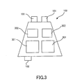
- FIG. 3 is a view illustrating an example of the arrangement of the IGBTs 301 and the diodes 302. Two IGBTs 301 are arranged closer to the long side of the power module 103, and two diodes 302 are arranged closer to the short side of the power module 103.
- the IGBT 301 tends to have a larger footprint when mounted and a larger heat generation amount than those of the diode 302. Accordingly, the IGBTs 301 are arranged closer to the long side in order to obtain a heat dissipation area for the IGBTs 301 whose heat generation amount is large. Consequently, an average temperature of the IGBTs 301 during the drive of the inverter can be reduced, and as a result, long-term reliability of the inverter module 2 can be improved.
- the IGBTs 301 whose mounting footprint is large are arranged closer to the long side, and the diodes 302 whose mounting footprint is small are arranged closer to the short side, and hence it is unnecessary to increase the short side and the long side in order only to mount the respective elements, and upsizing of the power module 103 can be avoided.
- control signal input/output terminals 401 of the power module 103 and gate pads 402 serving as control signal input pads of the IGBTs 301 is described.
- FIG. 4 is a view illustrating an example of the arrangement of the control signal input/output terminals 401 and the gate pads 402.
- the gate pad 402 of the IGBT 301 is arranged in proximity to any one of the four sides thereof.
- control signal input/output terminals 401 are arranged closer to the long side of the power module 103, and the IGBT 301 is mounted so that the gate pad 402 is located closer to the long side.
- the IGBT 301 is mounted in the state in which the gate pad 402 of the IGBT 301 is located in proximity to the control signal input/output terminals 401, and the parasitic inductance of the wiring of the gate drive circuit can be reduced to decrease the impedance generated in wiring between the gate pad 402 and the control signal input/output terminals 401. Further, it is unnecessary to newly provide an additional space for arranging the control signal input/output terminals 401, and hence the upsizing of the power module 103 can be suppressed.
- FIG. 5 is a view illustrating an example of the array of the control signal input/output terminals 401.
- the control signal input/output terminals 401 include six terminals as illustrated in FIG. 5 .
- lower arm switching element-use control signal input terminals 501 In the order starting from the terminal closest to the motor connection terminal 102, there are arranged lower arm switching element-use control signal input terminals 501, a lower arm switching element-use high potential-side potential sense terminal 502, upper arm switching element-use control signal input terminals 503, and an upper arm switching element-use high potential-side potential sense terminal 504.
- the switching element-use control signal input terminals 501 and 503 are gate and emitter sense terminals.
- the switching element-use high potential-side potential sense terminals 502 and 504 are emitter sense terminals.
- the above-mentioned terminals 501 to 504 have potentials different from one another during the operation of the inverter, and hence an insulation distance corresponding to a potential difference between the terminals needs to be secured between the terminals.
- the total sum of the insulation distances between the respective terminals can be further reduced, and as a result, the length required for the terminal array can be further reduced. Consequently, the power module 103 can be downsized to downsize the inverter module 2.
- the motor connection terminal 102 is arranged closer to the left end of the power module 103, and the terminals 501 to 504 are arranged in the above-mentioned order toward the right end thereof from the motor connection terminal 102.
- the motor connection terminal 102 may be arranged closer to the right end of FIG. 5
- the terminals 501 to 504 may be arranged in the above-mentioned order toward the left end thereof from the motor connection terminal 102.
- any of the gate and emitter terminals of the lower arm switching element-use control signal input terminals 501 may be arranged on the motor connection terminal 102 side. The same is true for the upper arm switching element-use control signal input terminals 503.
- the plurality of trapezoidal power modules 103 each of which has a single-phase inverter circuit mounted thereon and includes the power supply connection terminals 101 arranged on its short side and the motor connection terminal 102 arranged on its long side, are arranged in an annular pattern so that the long side of each of the plurality of trapezoidal power modules 103 faces toward the outer periphery, to thereby construct a polyphase inverter circuit.
- the motor connection terminals 102 are arranged at the outer periphery of the inverter module 2 in an annular pattern, and the space for the routing of the wiring 104 for electrically connecting the motor 1 and the inverter module 2 to each other and the space for the connection work can be reduced.
- the inverter module 2 can be downsized while the deterioration in electrical characteristics of the inverter module 2 is suppressed.
- the IGBT 301 is arranged closer to the long side, and the diode 302 is arranged closer to the short side, and hence the heat dissipation area for the IGBT 301 whose heat generation is particularly large can be obtained without increasing the surface area of the power module 103.
- the average temperature of the IGBTs 301 during the drive of the inverter can be reduced, and the long-term reliability of the inverter module 2 can be improved.
- the control signal input/output terminals 401 are arranged closer to the long side, and the IGBT 301 is mounted so that the gate pad 402 is located in proximity to the long side. Consequently, the parasitic inductance of the wiring of the IGBT gate drive circuit can be reduced while the upsizing of the power module 103 is suppressed. As a result, the low impedance of the IGBT gate drive circuit can be achieved, and the possibility of a malfunction of the inverter due to noise can be reduced to improve operational reliability of the inverter module 2.
- the motor connection terminal 102 and the control signal input/output terminals 401 are arranged in the order of the motor connection terminal 102, the lower arm switching element-use control signal input terminals 501, the lower arm switching element-use high potential-side potential sense terminal 502, the upper arm switching element-use control signal input terminals 503, and the upper arm switching element-use high potential-side potential sense terminal 504. Consequently, the insulation distances required for the respective terminals can be shortened, and hence the power module 301 can be downsized to further downsize the inverter module 2.
Landscapes
- Engineering & Computer Science (AREA)
- Power Engineering (AREA)
- Microelectronics & Electronic Packaging (AREA)
- Inverter Devices (AREA)
Abstract
Description
- This invention relates to an inverter module that is integrated with a motor.
- In
JP 2007-116840 A - In
JP 2007-116840 A - It is therefore an object of this invention to provide an inverter module for use in an inverter-integrated motor, which has a small space necessary for the wire routing and the connection work as described above.
- An inverter module according to one embodiment of this invention is an inverter module for use in an inverter-integrated motor, and includes a plurality of power modules each having a single-phase inverter circuit mounted thereon. The power module has a trapezoidal shape, and includes an electrical connection terminal for a power supply arranged on a short side thereof and an electrical connection terminal for the motor arranged on a long side thereof. The plurality of power modules are arranged in an annular pattern so that the long side of each of the plurality of power modules faces toward an outer periphery, to thereby construct a polyphase inverter circuit. In other words, the electrical connection terminals for the motor are arranged on an outer peripheral side of a polyphase module.
-
-
FIG. 1A is a horizontal sectional view of an inverter-integrated motor according to an embodiment of this invention. -
FIG. 1B is a sectional view taken along theline 1B-1B ofFIG. 1A . -
FIG. 2A is a horizontal sectional view of an inverter-integrated motor according to another example of the embodiment of this invention. -
FIG. 2B is a sectional view taken along theline 2B-2B ofFIG. 2A . -
FIG. 3 is a view illustrating an example of arrangement of switching elements and current reflux elements in a power module. -
FIG. 4 is a view illustrating an example of arrangement of control signal input/output terminals and control signal input pads. -
FIG. 5 is a view illustrating an example of array of the control signal input/ output terminals. - An embodiment of this invention is described below with reference to the drawings.
-
FIG. 1A is a schematic configuration diagram of an inverter-integrated motor according to this embodiment, and is a sectional view taken along a rotary shaft of anelectric motor 1.FIG. 1B is a sectional view taken along theline 1B-1B ofFIG. 1A . - In an inverter-integrated
motor 10, aninverter module 2 constructing a polyphase inverter circuit is mounted on amotor wall 1A that is provided at an end portion of the motor in the rotary shaft direction, which is a part of amotor casing 10A. It should be noted that the inverter-integratedmotor 10 is, for example, an AC motor for use as a drive motor for an electric vehicle, and is driven by electric power supplied from a DC power supply, such as an on-board battery, via theinverter module 2. - The
motor 1 includes a rotor 4 and astator 3. The rotor 4 rotates about the rotary shaft (not shown). Thestator 3 is arranged so as to surround an outer periphery of the rotor 4. - The
inverter module 2 is formed by arranging a plurality ofpower modules 103, each of which has a single-phase inverter circuit mounted thereon, in an annular pattern as described below. - As illustrated in
FIG. 1B , thepower module 103 has a trapezoidal cross-section, and includes powersupply connection terminals 101 on its short side, which serve as electrical connection terminals for a power supply (not shown), and amotor connection terminal 102 on its long side, which serves as an electrical connection terminal for themotor 1. Then, thepower modules 103 are arranged on themotor wall 1A on the inverter side in an annular pattern so that the short sides face toward the shaft center. Accordingly, themotor connection terminals 102 are arranged on an outer peripheral portion of theinverter module 2 in an annular pattern. - Wiring 104 for electrically connecting the
motor 1 and theinverter module 2 to each other is extracted from thestator 3 so as to pass through themotor wall 1A to be routed linearly to themotor connection terminal 102. InFIG. 1A and FIG. 1B , the position of themotor connection terminal 102 and the position of a through hole of themotor wall 1A for extracting thewiring 104 are aligned with each other to minimize the length of thewiring 104. - As described above, the
motor connection terminals 102 are arranged at the outer periphery of theinverter module 2 in an annular pattern, and hence thewiring 104 does not need to be bent unnecessarily but can electrically connect themotor 1 and theinverter module 2 to each other with a shorter length. Further, the electrical connection to themotor 1 is established on the outer peripheral side and the electrical connection to the power supply is established on the inner peripheral side, and hence the respective connection works are performed at different locations, and the work space can be reduced as compared to the case where both connection works are performed at a single location. In other words, the space for the routing of thewiring 104 and the space for the connection work can be reduced. Further, the reduction in length of thewiring 104 can reduce cost and radiated noise. - It should be noted that
FIG. 1A and FIG. 1B show an example in which theinverter module 2 is formed on themotor wall 1A, but theinverter module 2 may be formed on aninverter wall 2A that is opposed to themotor wall 1A as illustrated inFIG. 2A and FIG. 2B. FIG. 2A and FIG. 2B are views corresponding toFIG. 1A and FIG. 1B , respectively. - In this case, the
wiring 104 becomes longer than that inFIG. 1A and FIG. 1B , but the effects of the reduction in space for the routing of thewiring 104 and space for the connection work, the reduction in cost, and the reduction in radiated noise can be similarly obtained. - As described above, according to the configuration of
FIG. 1A and FIG. 1B orFIG. 2A and FIG. 2B , the space for the routing of thewiring 104 for electrically connecting themotor 1 and theinverter module 2 to each other and the space for the connection work can be reduced, and as a result, theinverter module 2 can be downsized while a deterioration in electrical characteristics of theinverter module 2 is suppressed. - Next, a switching element and a current reflux element to be mounted in the
power module 103 are described. A description is herein given using an insulated gate bipolar transistor (IGBT) 301 as an example of the switching element and adiode 302 as an example of the current reflux element. -
FIG. 3 is a view illustrating an example of the arrangement of theIGBTs 301 and thediodes 302. TwoIGBTs 301 are arranged closer to the long side of thepower module 103, and twodiodes 302 are arranged closer to the short side of thepower module 103. - In general, the
IGBT 301 tends to have a larger footprint when mounted and a larger heat generation amount than those of thediode 302. Accordingly, theIGBTs 301 are arranged closer to the long side in order to obtain a heat dissipation area for theIGBTs 301 whose heat generation amount is large. Consequently, an average temperature of theIGBTs 301 during the drive of the inverter can be reduced, and as a result, long-term reliability of theinverter module 2 can be improved. - Further, the
IGBTs 301 whose mounting footprint is large are arranged closer to the long side, and thediodes 302 whose mounting footprint is small are arranged closer to the short side, and hence it is unnecessary to increase the short side and the long side in order only to mount the respective elements, and upsizing of thepower module 103 can be avoided. - Next, the arrangement of control signal input/
output terminals 401 of thepower module 103 andgate pads 402 serving as control signal input pads of theIGBTs 301 is described. -
FIG. 4 is a view illustrating an example of the arrangement of the control signal input/output terminals 401 and thegate pads 402. In this case, thegate pad 402 of theIGBT 301 is arranged in proximity to any one of the four sides thereof. - In an inverter configured to perform switching operation, noise due to an abrupt change in voltage and current is generated in principle. In order to suppress a malfunction of the inverter itself due to the noise, it is necessary to design an IGBT gate drive circuit to have low impedance. In particular, reducing parasitic inductance of wiring of the gate drive circuit is a primary design factor for achieving low impedance.
- Then, as illustrated in
FIG. 4 , the control signal input/output terminals 401 are arranged closer to the long side of thepower module 103, and theIGBT 301 is mounted so that thegate pad 402 is located closer to the long side. - Accordingly, the
IGBT 301 is mounted in the state in which thegate pad 402 of theIGBT 301 is located in proximity to the control signal input/output terminals 401, and the parasitic inductance of the wiring of the gate drive circuit can be reduced to decrease the impedance generated in wiring between thegate pad 402 and the control signal input/output terminals 401. Further, it is unnecessary to newly provide an additional space for arranging the control signal input/output terminals 401, and hence the upsizing of thepower module 103 can be suppressed. - Next, the array of the control signal input/
output terminals 401 is described. -
FIG. 5 is a view illustrating an example of the array of the control signal input/output terminals 401. The control signal input/output terminals 401 include six terminals as illustrated inFIG. 5 . In the order starting from the terminal closest to themotor connection terminal 102, there are arranged lower arm switching element-use controlsignal input terminals 501, a lower arm switching element-use high potential-sidepotential sense terminal 502, upper arm switching element-use controlsignal input terminals 503, and an upper arm switching element-use high potential-sidepotential sense terminal 504. - Taking the
IGBT 301 as an example, the switching element-use controlsignal input terminals IGBT 301 as an example, the switching element-use high potential-sidepotential sense terminals - The above-mentioned
terminals 501 to 504 have potentials different from one another during the operation of the inverter, and hence an insulation distance corresponding to a potential difference between the terminals needs to be secured between the terminals. By arraying theterminals 501 to 504 as illustrated inFIG. 5 , the total sum of the insulation distances between the respective terminals can be further reduced, and as a result, the length required for the terminal array can be further reduced. Consequently, thepower module 103 can be downsized to downsize theinverter module 2. - It should be noted that in
FIG. 5 themotor connection terminal 102 is arranged closer to the left end of thepower module 103, and theterminals 501 to 504 are arranged in the above-mentioned order toward the right end thereof from themotor connection terminal 102. Alternatively, however, themotor connection terminal 102 may be arranged closer to the right end ofFIG. 5 , and theterminals 501 to 504 may be arranged in the above-mentioned order toward the left end thereof from themotor connection terminal 102. Further, any of the gate and emitter terminals of the lower arm switching element-use controlsignal input terminals 501 may be arranged on themotor connection terminal 102 side. The same is true for the upper arm switching element-use controlsignal input terminals 503. - The actions and effects of this embodiment described above are summarized below.
- The plurality of
trapezoidal power modules 103, each of which has a single-phase inverter circuit mounted thereon and includes the powersupply connection terminals 101 arranged on its short side and themotor connection terminal 102 arranged on its long side, are arranged in an annular pattern so that the long side of each of the plurality oftrapezoidal power modules 103 faces toward the outer periphery, to thereby construct a polyphase inverter circuit. Accordingly, themotor connection terminals 102 are arranged at the outer periphery of theinverter module 2 in an annular pattern, and the space for the routing of thewiring 104 for electrically connecting themotor 1 and theinverter module 2 to each other and the space for the connection work can be reduced. As a result, theinverter module 2 can be downsized while the deterioration in electrical characteristics of theinverter module 2 is suppressed. - In the
power module 103, theIGBT 301 is arranged closer to the long side, and thediode 302 is arranged closer to the short side, and hence the heat dissipation area for theIGBT 301 whose heat generation is particularly large can be obtained without increasing the surface area of thepower module 103. As a result, the average temperature of theIGBTs 301 during the drive of the inverter can be reduced, and the long-term reliability of theinverter module 2 can be improved. - The control signal input/
output terminals 401 are arranged closer to the long side, and theIGBT 301 is mounted so that thegate pad 402 is located in proximity to the long side. Consequently, the parasitic inductance of the wiring of the IGBT gate drive circuit can be reduced while the upsizing of thepower module 103 is suppressed. As a result, the low impedance of the IGBT gate drive circuit can be achieved, and the possibility of a malfunction of the inverter due to noise can be reduced to improve operational reliability of theinverter module 2. - The
motor connection terminal 102 and the control signal input/output terminals 401 are arranged in the order of themotor connection terminal 102, the lower arm switching element-use controlsignal input terminals 501, the lower arm switching element-use high potential-sidepotential sense terminal 502, the upper arm switching element-use controlsignal input terminals 503, and the upper arm switching element-use high potential-sidepotential sense terminal 504. Consequently, the insulation distances required for the respective terminals can be shortened, and hence thepower module 301 can be downsized to further downsize theinverter module 2. - Although a description above has been given of the embodiment of this invention, the embodiment above describes only a part of application examples of this invention, and is not intended to limit the technical scope of this invention to the specific configurations of the above-mentioned embodiment.
- This application claims priority from Japanese Patent Application No.
2012-51928, filed on March 8, 2012
Claims (2)
- An inverter module for use in an inverter-integrated motor,
the inverter module being arranged at an axial end portion of a motor,
the inverter module comprising trapezoidal power modules, each of which has a single-phase inverter circuit mounted thereon, and includes an electrical connection terminal for a power supply arranged on a short side thereof and an electrical connection terminal for the motor arranged on a long side thereof,
wherein a polyphase inverter circuit is constructed by arranging a plurality of the trapezoidal power modules in an annular pattern so that the long side of the each of the plurality of the power modules faces toward an outer periphery. - The inverter module according to claim 1,
wherein the power modules comprises:control signal input/output terminals arranged on the long side; anda switching element mounted closer to the long side in a direction in which a control signal input pad is located in proximity to the long side, and a current reflux element mounted closer to the short side, the current reflux element being electrically connected in parallel to the switching element, andwherein the electrical connection terminal for the motor and the control signal input/output terminals are arranged in order of the electrical connection terminal for the motor, a lower arm switching element-use control signal input terminal, a lower arm switching element-use high potential-side potential sense terminal, an upper arm switching element-use control signal input terminal, and an upper arm switching element-use high potential-side potential sense terminal.
Applications Claiming Priority (2)
| Application Number | Priority Date | Filing Date | Title |
|---|---|---|---|
| JP2012051928A JP5888010B2 (en) | 2012-03-08 | 2012-03-08 | Inverter module |
| PCT/JP2013/054091 WO2013133014A1 (en) | 2012-03-08 | 2013-02-20 | Inverter module |
Publications (3)
| Publication Number | Publication Date |
|---|---|
| EP2824820A1 true EP2824820A1 (en) | 2015-01-14 |
| EP2824820A4 EP2824820A4 (en) | 2015-11-18 |
| EP2824820B1 EP2824820B1 (en) | 2016-09-14 |
Family
ID=49116497
Family Applications (1)
| Application Number | Title | Priority Date | Filing Date |
|---|---|---|---|
| EP13757205.3A Active EP2824820B1 (en) | 2012-03-08 | 2013-02-20 | Inverter module |
Country Status (5)
| Country | Link |
|---|---|
| US (1) | US9502946B2 (en) |
| EP (1) | EP2824820B1 (en) |
| JP (1) | JP5888010B2 (en) |
| CN (1) | CN104205599B (en) |
| WO (1) | WO2013133014A1 (en) |
Cited By (2)
| Publication number | Priority date | Publication date | Assignee | Title |
|---|---|---|---|---|
| DE102015014509A1 (en) * | 2015-11-11 | 2017-05-11 | Bergische Universität Wuppertal | Electric drive system |
| DE102016220617A1 (en) * | 2016-10-20 | 2018-04-26 | Mahle International Gmbh | Electric motor for a motor vehicle |
Families Citing this family (9)
| Publication number | Priority date | Publication date | Assignee | Title |
|---|---|---|---|---|
| JP6149663B2 (en) * | 2013-10-03 | 2017-06-21 | 日産自動車株式会社 | Mechanical and electric integrated motor |
| CN106165280B (en) | 2014-04-08 | 2018-12-14 | 三菱电机株式会社 | It is molded module |
| US10491083B2 (en) | 2015-05-29 | 2019-11-26 | Shindengen Electric Manufacturing Co., Ltd. | Semiconductor device and semiconductor device mounting method |
| EP3321117B1 (en) * | 2015-07-07 | 2020-05-13 | Nissan Motor Co., Ltd. | Arrangement structure for wheel drive device |
| JP2017199827A (en) * | 2016-04-28 | 2017-11-02 | 三菱電機株式会社 | Power semiconductor device |
| JP6576502B1 (en) * | 2018-04-11 | 2019-09-18 | 三菱電機株式会社 | Power semiconductor device |
| JP7159618B2 (en) | 2018-05-25 | 2022-10-25 | 富士電機株式会社 | Semiconductor modules and power converters |
| JP7202979B2 (en) | 2019-06-13 | 2023-01-12 | 株式会社Soken | power converter |
| JP7601301B2 (en) * | 2020-11-30 | 2024-12-17 | ニデックエレシス株式会社 | Capacitor module, inverter module and motor unit |
Family Cites Families (26)
| Publication number | Priority date | Publication date | Assignee | Title |
|---|---|---|---|---|
| US5512790A (en) * | 1994-07-21 | 1996-04-30 | Delco Electronics Corporation | Triaxial double switch module |
| US6377478B1 (en) * | 1999-05-28 | 2002-04-23 | Toshiba International Corporation | Inverter device |
| JP4054137B2 (en) * | 1999-06-03 | 2008-02-27 | 株式会社東京アールアンドデー | Power semiconductor element power supply and heat dissipation device |
| JP4009056B2 (en) * | 2000-05-25 | 2007-11-14 | 三菱電機株式会社 | Power module |
| JP3743433B2 (en) * | 2003-03-25 | 2006-02-08 | 日産自動車株式会社 | Power converter |
| JP4034766B2 (en) * | 2004-08-18 | 2008-01-16 | 東芝コンシューママーケティング株式会社 | Circuit board and electric blower |
| US7210304B2 (en) * | 2005-02-09 | 2007-05-01 | General Motors Corporation | Cooling arrangements for integrated electric motor-inverters |
| JP4478049B2 (en) * | 2005-03-15 | 2010-06-09 | 三菱電機株式会社 | Semiconductor device |
| JP4708951B2 (en) * | 2005-10-21 | 2011-06-22 | ニチコン株式会社 | Inverter module and inverter-integrated AC motor using the same |
| JP2008099460A (en) * | 2006-10-13 | 2008-04-24 | Nissan Motor Co Ltd | Power converter |
| JP4899819B2 (en) * | 2006-11-22 | 2012-03-21 | 日産自動車株式会社 | Power conversion device for motor / electric motor |
| JP5205595B2 (en) * | 2006-12-07 | 2013-06-05 | 日産自動車株式会社 | Power converter and motor drive system |
| FR2911444B1 (en) * | 2006-12-22 | 2016-02-12 | Valeo Equip Electr Moteur | CURRENT RECTIFIER DEVICE FOR ROTATING ELECTRIC MACHINE AND ROTATING ELECTRIC MACHINE COMPRISING SUCH A DEVICE |
| JP5211544B2 (en) * | 2007-05-07 | 2013-06-12 | 日産自動車株式会社 | Semiconductor device |
| JP5333814B2 (en) * | 2007-09-12 | 2013-11-06 | アイシン精機株式会社 | Power semiconductor module, inverter device, and inverter-integrated motor |
| JP4811749B2 (en) * | 2009-06-24 | 2011-11-09 | 株式会社デンソー | Drive device |
| JP5327646B2 (en) * | 2009-06-24 | 2013-10-30 | 株式会社デンソー | Motor with built-in electronic circuit |
| JP5471114B2 (en) * | 2009-07-24 | 2014-04-16 | 日産自動車株式会社 | Inverter device |
| GB2462940B8 (en) * | 2009-09-03 | 2012-03-28 | Protean Holdings Corp | Electric motor and electric generator. |
| CN102142756B (en) * | 2010-01-28 | 2013-11-06 | 株式会社电装 | Motor |
| JP5126277B2 (en) * | 2010-04-16 | 2013-01-23 | 株式会社デンソー | Electric device |
| JP5719524B2 (en) * | 2010-04-16 | 2015-05-20 | 株式会社デンソー | Electric device |
| JP5516187B2 (en) | 2010-07-27 | 2014-06-11 | 日産自動車株式会社 | Power converter |
| US9123693B2 (en) * | 2011-04-07 | 2015-09-01 | Mitsubishi Electric Corporation | Mold module utilized as power unit of electric power steering apparatus and electric power steering apparatus |
| JP5805513B2 (en) * | 2011-12-14 | 2015-11-04 | 三菱電機株式会社 | Power semiconductor device |
| JP2013187998A (en) * | 2012-03-07 | 2013-09-19 | Nissan Motor Co Ltd | Electric power conversion system |
-
2012
- 2012-03-08 JP JP2012051928A patent/JP5888010B2/en active Active
-
2013
- 2013-02-20 WO PCT/JP2013/054091 patent/WO2013133014A1/en not_active Ceased
- 2013-02-20 EP EP13757205.3A patent/EP2824820B1/en active Active
- 2013-02-20 CN CN201380012460.XA patent/CN104205599B/en active Active
- 2013-02-20 US US14/382,466 patent/US9502946B2/en active Active
Cited By (2)
| Publication number | Priority date | Publication date | Assignee | Title |
|---|---|---|---|---|
| DE102015014509A1 (en) * | 2015-11-11 | 2017-05-11 | Bergische Universität Wuppertal | Electric drive system |
| DE102016220617A1 (en) * | 2016-10-20 | 2018-04-26 | Mahle International Gmbh | Electric motor for a motor vehicle |
Also Published As
| Publication number | Publication date |
|---|---|
| WO2013133014A1 (en) | 2013-09-12 |
| JP2013188027A (en) | 2013-09-19 |
| CN104205599B (en) | 2017-03-08 |
| CN104205599A (en) | 2014-12-10 |
| EP2824820A4 (en) | 2015-11-18 |
| JP5888010B2 (en) | 2016-03-16 |
| US9502946B2 (en) | 2016-11-22 |
| EP2824820B1 (en) | 2016-09-14 |
| US20150097470A1 (en) | 2015-04-09 |
Similar Documents
| Publication | Publication Date | Title |
|---|---|---|
| EP2824820B1 (en) | Inverter module | |
| US8693193B2 (en) | Power converter | |
| CN108137084B (en) | Integrated electric power steering device and manufacturing method thereof | |
| JP3760887B2 (en) | Inverter integrated motor for vehicles | |
| JP4583191B2 (en) | Rotating electric machine | |
| CN101617460B (en) | Brushless motor | |
| US10523091B2 (en) | Control unit and electric power steering device employing control unit | |
| JPWO2017046940A1 (en) | Integrated electric power steering system | |
| JPH10322973A (en) | Electric motor with power converter | |
| US20180191220A1 (en) | Electric compressor | |
| CN111108668B (en) | Electric power steering apparatus | |
| CN105406652A (en) | Power Conversion Device | |
| JP6362770B2 (en) | Control device | |
| JP5558534B2 (en) | Rotating electric machine | |
| JP2015095486A (en) | Semiconductor device | |
| JP4045923B2 (en) | Electric motor | |
| CN113826315B (en) | Power conversion device | |
| JP2008099397A (en) | Smoothing capacitor module and power converter using the same | |
| US10629521B2 (en) | Molded module | |
| JP4946241B2 (en) | AC controller structure | |
| US11990799B2 (en) | Capacitor module, inverter module, and motor unit | |
| KR102393490B1 (en) | Motor | |
| CN111245167A (en) | Integrated motor | |
| JPWO2014045499A1 (en) | Power converter | |
| KR20230141145A (en) | Inverter Package |
Legal Events
| Date | Code | Title | Description |
|---|---|---|---|
| PUAI | Public reference made under article 153(3) epc to a published international application that has entered the european phase |
Free format text: ORIGINAL CODE: 0009012 |
|
| 17P | Request for examination filed |
Effective date: 20141008 |
|
| AK | Designated contracting states |
Kind code of ref document: A1 Designated state(s): AL AT BE BG CH CY CZ DE DK EE ES FI FR GB GR HR HU IE IS IT LI LT LU LV MC MK MT NL NO PL PT RO RS SE SI SK SM TR |
|
| AX | Request for extension of the european patent |
Extension state: BA ME |
|
| DAX | Request for extension of the european patent (deleted) | ||
| RA4 | Supplementary search report drawn up and despatched (corrected) |
Effective date: 20151016 |
|
| RIC1 | Information provided on ipc code assigned before grant |
Ipc: H02M 7/00 20060101ALI20151012BHEP Ipc: H02M 7/48 20070101AFI20151012BHEP Ipc: H02K 3/52 20060101ALI20151012BHEP Ipc: H02K 11/00 20060101ALI20151012BHEP |
|
| GRAP | Despatch of communication of intention to grant a patent |
Free format text: ORIGINAL CODE: EPIDOSNIGR1 |
|
| INTG | Intention to grant announced |
Effective date: 20160122 |
|
| RAP1 | Party data changed (applicant data changed or rights of an application transferred) |
Owner name: NISSAN MOTOR CO., LTD. |
|
| RIN1 | Information on inventor provided before grant (corrected) |
Inventor name: MIZUKOSHI, YUKIO Inventor name: SASAKI, KENSUKE Inventor name: NAKAYAMA, HIROYUKI |
|
| GRAP | Despatch of communication of intention to grant a patent |
Free format text: ORIGINAL CODE: EPIDOSNIGR1 |
|
| RIC1 | Information provided on ipc code assigned before grant |
Ipc: H02M 7/48 20070101AFI20160429BHEP Ipc: H02K 3/52 20060101ALI20160429BHEP Ipc: H02M 7/00 20060101ALI20160429BHEP Ipc: H02K 11/33 20160101ALI20160429BHEP |
|
| INTG | Intention to grant announced |
Effective date: 20160520 |
|
| GRAS | Grant fee paid |
Free format text: ORIGINAL CODE: EPIDOSNIGR3 |
|
| GRAA | (expected) grant |
Free format text: ORIGINAL CODE: 0009210 |
|
| AK | Designated contracting states |
Kind code of ref document: B1 Designated state(s): AL AT BE BG CH CY CZ DE DK EE ES FI FR GB GR HR HU IE IS IT LI LT LU LV MC MK MT NL NO PL PT RO RS SE SI SK SM TR |
|
| REG | Reference to a national code |
Ref country code: GB Ref legal event code: FG4D |
|
| REG | Reference to a national code |
Ref country code: CH Ref legal event code: EP |
|
| REG | Reference to a national code |
Ref country code: IE Ref legal event code: FG4D |
|
| REG | Reference to a national code |
Ref country code: AT Ref legal event code: REF Ref document number: 829967 Country of ref document: AT Kind code of ref document: T Effective date: 20161015 |
|
| REG | Reference to a national code |
Ref country code: DE Ref legal event code: R096 Ref document number: 602013011653 Country of ref document: DE |
|
| REG | Reference to a national code |
Ref country code: FR Ref legal event code: PLFP Year of fee payment: 5 |
|
| REG | Reference to a national code |
Ref country code: LT Ref legal event code: MG4D |
|
| REG | Reference to a national code |
Ref country code: NL Ref legal event code: MP Effective date: 20160914 |
|
| PG25 | Lapsed in a contracting state [announced via postgrant information from national office to epo] |
Ref country code: NO Free format text: LAPSE BECAUSE OF FAILURE TO SUBMIT A TRANSLATION OF THE DESCRIPTION OR TO PAY THE FEE WITHIN THE PRESCRIBED TIME-LIMIT Effective date: 20161214 Ref country code: FI Free format text: LAPSE BECAUSE OF FAILURE TO SUBMIT A TRANSLATION OF THE DESCRIPTION OR TO PAY THE FEE WITHIN THE PRESCRIBED TIME-LIMIT Effective date: 20160914 Ref country code: LT Free format text: LAPSE BECAUSE OF FAILURE TO SUBMIT A TRANSLATION OF THE DESCRIPTION OR TO PAY THE FEE WITHIN THE PRESCRIBED TIME-LIMIT Effective date: 20160914 Ref country code: HR Free format text: LAPSE BECAUSE OF FAILURE TO SUBMIT A TRANSLATION OF THE DESCRIPTION OR TO PAY THE FEE WITHIN THE PRESCRIBED TIME-LIMIT Effective date: 20160914 Ref country code: RS Free format text: LAPSE BECAUSE OF FAILURE TO SUBMIT A TRANSLATION OF THE DESCRIPTION OR TO PAY THE FEE WITHIN THE PRESCRIBED TIME-LIMIT Effective date: 20160914 |
|
| REG | Reference to a national code |
Ref country code: AT Ref legal event code: MK05 Ref document number: 829967 Country of ref document: AT Kind code of ref document: T Effective date: 20160914 |
|
| PG25 | Lapsed in a contracting state [announced via postgrant information from national office to epo] |
Ref country code: GR Free format text: LAPSE BECAUSE OF FAILURE TO SUBMIT A TRANSLATION OF THE DESCRIPTION OR TO PAY THE FEE WITHIN THE PRESCRIBED TIME-LIMIT Effective date: 20161215 Ref country code: LV Free format text: LAPSE BECAUSE OF FAILURE TO SUBMIT A TRANSLATION OF THE DESCRIPTION OR TO PAY THE FEE WITHIN THE PRESCRIBED TIME-LIMIT Effective date: 20160914 Ref country code: NL Free format text: LAPSE BECAUSE OF FAILURE TO SUBMIT A TRANSLATION OF THE DESCRIPTION OR TO PAY THE FEE WITHIN THE PRESCRIBED TIME-LIMIT Effective date: 20160914 Ref country code: SE Free format text: LAPSE BECAUSE OF FAILURE TO SUBMIT A TRANSLATION OF THE DESCRIPTION OR TO PAY THE FEE WITHIN THE PRESCRIBED TIME-LIMIT Effective date: 20160914 |
|
| PG25 | Lapsed in a contracting state [announced via postgrant information from national office to epo] |
Ref country code: EE Free format text: LAPSE BECAUSE OF FAILURE TO SUBMIT A TRANSLATION OF THE DESCRIPTION OR TO PAY THE FEE WITHIN THE PRESCRIBED TIME-LIMIT Effective date: 20160914 Ref country code: RO Free format text: LAPSE BECAUSE OF FAILURE TO SUBMIT A TRANSLATION OF THE DESCRIPTION OR TO PAY THE FEE WITHIN THE PRESCRIBED TIME-LIMIT Effective date: 20160914 |
|
| PG25 | Lapsed in a contracting state [announced via postgrant information from national office to epo] |
Ref country code: BE Free format text: LAPSE BECAUSE OF FAILURE TO SUBMIT A TRANSLATION OF THE DESCRIPTION OR TO PAY THE FEE WITHIN THE PRESCRIBED TIME-LIMIT Effective date: 20160914 Ref country code: ES Free format text: LAPSE BECAUSE OF FAILURE TO SUBMIT A TRANSLATION OF THE DESCRIPTION OR TO PAY THE FEE WITHIN THE PRESCRIBED TIME-LIMIT Effective date: 20160914 Ref country code: PL Free format text: LAPSE BECAUSE OF FAILURE TO SUBMIT A TRANSLATION OF THE DESCRIPTION OR TO PAY THE FEE WITHIN THE PRESCRIBED TIME-LIMIT Effective date: 20160914 Ref country code: CZ Free format text: LAPSE BECAUSE OF FAILURE TO SUBMIT A TRANSLATION OF THE DESCRIPTION OR TO PAY THE FEE WITHIN THE PRESCRIBED TIME-LIMIT Effective date: 20160914 Ref country code: IS Free format text: LAPSE BECAUSE OF FAILURE TO SUBMIT A TRANSLATION OF THE DESCRIPTION OR TO PAY THE FEE WITHIN THE PRESCRIBED TIME-LIMIT Effective date: 20170114 Ref country code: SK Free format text: LAPSE BECAUSE OF FAILURE TO SUBMIT A TRANSLATION OF THE DESCRIPTION OR TO PAY THE FEE WITHIN THE PRESCRIBED TIME-LIMIT Effective date: 20160914 Ref country code: SM Free format text: LAPSE BECAUSE OF FAILURE TO SUBMIT A TRANSLATION OF THE DESCRIPTION OR TO PAY THE FEE WITHIN THE PRESCRIBED TIME-LIMIT Effective date: 20160914 Ref country code: AT Free format text: LAPSE BECAUSE OF FAILURE TO SUBMIT A TRANSLATION OF THE DESCRIPTION OR TO PAY THE FEE WITHIN THE PRESCRIBED TIME-LIMIT Effective date: 20160914 Ref country code: PT Free format text: LAPSE BECAUSE OF FAILURE TO SUBMIT A TRANSLATION OF THE DESCRIPTION OR TO PAY THE FEE WITHIN THE PRESCRIBED TIME-LIMIT Effective date: 20170116 Ref country code: BG Free format text: LAPSE BECAUSE OF FAILURE TO SUBMIT A TRANSLATION OF THE DESCRIPTION OR TO PAY THE FEE WITHIN THE PRESCRIBED TIME-LIMIT Effective date: 20161214 |
|
| REG | Reference to a national code |
Ref country code: DE Ref legal event code: R097 Ref document number: 602013011653 Country of ref document: DE |
|
| PG25 | Lapsed in a contracting state [announced via postgrant information from national office to epo] |
Ref country code: IT Free format text: LAPSE BECAUSE OF FAILURE TO SUBMIT A TRANSLATION OF THE DESCRIPTION OR TO PAY THE FEE WITHIN THE PRESCRIBED TIME-LIMIT Effective date: 20160914 |
|
| PLBE | No opposition filed within time limit |
Free format text: ORIGINAL CODE: 0009261 |
|
| STAA | Information on the status of an ep patent application or granted ep patent |
Free format text: STATUS: NO OPPOSITION FILED WITHIN TIME LIMIT |
|
| PG25 | Lapsed in a contracting state [announced via postgrant information from national office to epo] |
Ref country code: DK Free format text: LAPSE BECAUSE OF FAILURE TO SUBMIT A TRANSLATION OF THE DESCRIPTION OR TO PAY THE FEE WITHIN THE PRESCRIBED TIME-LIMIT Effective date: 20160914 |
|
| 26N | No opposition filed |
Effective date: 20170615 |
|
| PG25 | Lapsed in a contracting state [announced via postgrant information from national office to epo] |
Ref country code: MC Free format text: LAPSE BECAUSE OF FAILURE TO SUBMIT A TRANSLATION OF THE DESCRIPTION OR TO PAY THE FEE WITHIN THE PRESCRIBED TIME-LIMIT Effective date: 20160914 |
|
| REG | Reference to a national code |
Ref country code: CH Ref legal event code: PL |
|
| PG25 | Lapsed in a contracting state [announced via postgrant information from national office to epo] |
Ref country code: LI Free format text: LAPSE BECAUSE OF NON-PAYMENT OF DUE FEES Effective date: 20170228 Ref country code: CH Free format text: LAPSE BECAUSE OF NON-PAYMENT OF DUE FEES Effective date: 20170228 |
|
| REG | Reference to a national code |
Ref country code: IE Ref legal event code: MM4A |
|
| PG25 | Lapsed in a contracting state [announced via postgrant information from national office to epo] |
Ref country code: SI Free format text: LAPSE BECAUSE OF FAILURE TO SUBMIT A TRANSLATION OF THE DESCRIPTION OR TO PAY THE FEE WITHIN THE PRESCRIBED TIME-LIMIT Effective date: 20160914 |
|
| PG25 | Lapsed in a contracting state [announced via postgrant information from national office to epo] |
Ref country code: LU Free format text: LAPSE BECAUSE OF NON-PAYMENT OF DUE FEES Effective date: 20170220 |
|
| REG | Reference to a national code |
Ref country code: FR Ref legal event code: PLFP Year of fee payment: 6 |
|
| PG25 | Lapsed in a contracting state [announced via postgrant information from national office to epo] |
Ref country code: IE Free format text: LAPSE BECAUSE OF NON-PAYMENT OF DUE FEES Effective date: 20170220 |
|
| PG25 | Lapsed in a contracting state [announced via postgrant information from national office to epo] |
Ref country code: MT Free format text: LAPSE BECAUSE OF NON-PAYMENT OF DUE FEES Effective date: 20170220 |
|
| PG25 | Lapsed in a contracting state [announced via postgrant information from national office to epo] |
Ref country code: AL Free format text: LAPSE BECAUSE OF FAILURE TO SUBMIT A TRANSLATION OF THE DESCRIPTION OR TO PAY THE FEE WITHIN THE PRESCRIBED TIME-LIMIT Effective date: 20160914 |
|
| PG25 | Lapsed in a contracting state [announced via postgrant information from national office to epo] |
Ref country code: HU Free format text: LAPSE BECAUSE OF FAILURE TO SUBMIT A TRANSLATION OF THE DESCRIPTION OR TO PAY THE FEE WITHIN THE PRESCRIBED TIME-LIMIT; INVALID AB INITIO Effective date: 20130220 |
|
| PG25 | Lapsed in a contracting state [announced via postgrant information from national office to epo] |
Ref country code: CY Free format text: LAPSE BECAUSE OF FAILURE TO SUBMIT A TRANSLATION OF THE DESCRIPTION OR TO PAY THE FEE WITHIN THE PRESCRIBED TIME-LIMIT Effective date: 20160914 |
|
| PG25 | Lapsed in a contracting state [announced via postgrant information from national office to epo] |
Ref country code: MK Free format text: LAPSE BECAUSE OF FAILURE TO SUBMIT A TRANSLATION OF THE DESCRIPTION OR TO PAY THE FEE WITHIN THE PRESCRIBED TIME-LIMIT Effective date: 20160914 |
|
| PG25 | Lapsed in a contracting state [announced via postgrant information from national office to epo] |
Ref country code: TR Free format text: LAPSE BECAUSE OF FAILURE TO SUBMIT A TRANSLATION OF THE DESCRIPTION OR TO PAY THE FEE WITHIN THE PRESCRIBED TIME-LIMIT Effective date: 20160914 |
|
| PGFP | Annual fee paid to national office [announced via postgrant information from national office to epo] |
Ref country code: GB Payment date: 20260121 Year of fee payment: 14 |
|
| PGFP | Annual fee paid to national office [announced via postgrant information from national office to epo] |
Ref country code: DE Payment date: 20260121 Year of fee payment: 14 |
|
| PGFP | Annual fee paid to national office [announced via postgrant information from national office to epo] |
Ref country code: FR Payment date: 20260121 Year of fee payment: 14 |