EP2820678B1 - Integration of gallium nitride leds with aluminum gallium nitride/gallium nitride devices on silicon substrates for ac leds - Google Patents
Integration of gallium nitride leds with aluminum gallium nitride/gallium nitride devices on silicon substrates for ac leds Download PDFInfo
- Publication number
- EP2820678B1 EP2820678B1 EP13718387.7A EP13718387A EP2820678B1 EP 2820678 B1 EP2820678 B1 EP 2820678B1 EP 13718387 A EP13718387 A EP 13718387A EP 2820678 B1 EP2820678 B1 EP 2820678B1
- Authority
- EP
- European Patent Office
- Prior art keywords
- gan
- layer
- over
- stack
- substrate
- Prior art date
- Legal status (The legal status is an assumption and is not a legal conclusion. Google has not performed a legal analysis and makes no representation as to the accuracy of the status listed.)
- Active
Links
Images



Classifications
-
- H—ELECTRICITY
- H10—SEMICONDUCTOR DEVICES; ELECTRIC SOLID-STATE DEVICES NOT OTHERWISE PROVIDED FOR
- H10H—INORGANIC LIGHT-EMITTING SEMICONDUCTOR DEVICES HAVING POTENTIAL BARRIERS
- H10H20/00—Individual inorganic light-emitting semiconductor devices having potential barriers, e.g. light-emitting diodes [LED]
- H10H20/01—Manufacture or treatment
- H10H20/011—Manufacture or treatment of bodies, e.g. forming semiconductor layers
- H10H20/013—Manufacture or treatment of bodies, e.g. forming semiconductor layers having light-emitting regions comprising only Group III-V materials
- H10H20/0133—Manufacture or treatment of bodies, e.g. forming semiconductor layers having light-emitting regions comprising only Group III-V materials with a substrate not being Group III-V materials
- H10H20/01335—Manufacture or treatment of bodies, e.g. forming semiconductor layers having light-emitting regions comprising only Group III-V materials with a substrate not being Group III-V materials the light-emitting regions comprising nitride materials
-
- H—ELECTRICITY
- H10—SEMICONDUCTOR DEVICES; ELECTRIC SOLID-STATE DEVICES NOT OTHERWISE PROVIDED FOR
- H10H—INORGANIC LIGHT-EMITTING SEMICONDUCTOR DEVICES HAVING POTENTIAL BARRIERS
- H10H29/00—Integrated devices, or assemblies of multiple devices, comprising at least one light-emitting semiconductor element covered by group H10H20/00
- H10H29/10—Integrated devices comprising at least one light-emitting semiconductor component covered by group H10H20/00
-
- H—ELECTRICITY
- H10—SEMICONDUCTOR DEVICES; ELECTRIC SOLID-STATE DEVICES NOT OTHERWISE PROVIDED FOR
- H10D—INORGANIC ELECTRIC SEMICONDUCTOR DEVICES
- H10D88/00—Three-dimensional [3D] integrated devices
- H10D88/101—Three-dimensional [3D] integrated devices comprising components on opposite major surfaces of semiconductor substrates
-
- H—ELECTRICITY
- H10—SEMICONDUCTOR DEVICES; ELECTRIC SOLID-STATE DEVICES NOT OTHERWISE PROVIDED FOR
- H10D—INORGANIC ELECTRIC SEMICONDUCTOR DEVICES
- H10D84/00—Integrated devices formed in or on semiconductor substrates that comprise only semiconducting layers, e.g. on Si wafers or on GaAs-on-Si wafers
- H10D84/01—Manufacture or treatment
-
- H—ELECTRICITY
- H10—SEMICONDUCTOR DEVICES; ELECTRIC SOLID-STATE DEVICES NOT OTHERWISE PROVIDED FOR
- H10H—INORGANIC LIGHT-EMITTING SEMICONDUCTOR DEVICES HAVING POTENTIAL BARRIERS
- H10H20/00—Individual inorganic light-emitting semiconductor devices having potential barriers, e.g. light-emitting diodes [LED]
- H10H20/052—Light-emitting semiconductor devices having Schottky type light-emitting regions; Light emitting semiconductor devices having Metal-Insulator-Semiconductor type light-emitting regions
-
- H—ELECTRICITY
- H10—SEMICONDUCTOR DEVICES; ELECTRIC SOLID-STATE DEVICES NOT OTHERWISE PROVIDED FOR
- H10H—INORGANIC LIGHT-EMITTING SEMICONDUCTOR DEVICES HAVING POTENTIAL BARRIERS
- H10H20/00—Individual inorganic light-emitting semiconductor devices having potential barriers, e.g. light-emitting diodes [LED]
- H10H20/80—Constructional details
- H10H20/81—Bodies
- H10H20/811—Bodies having quantum effect structures or superlattices, e.g. tunnel junctions
-
- H—ELECTRICITY
- H10—SEMICONDUCTOR DEVICES; ELECTRIC SOLID-STATE DEVICES NOT OTHERWISE PROVIDED FOR
- H10H—INORGANIC LIGHT-EMITTING SEMICONDUCTOR DEVICES HAVING POTENTIAL BARRIERS
- H10H20/00—Individual inorganic light-emitting semiconductor devices having potential barriers, e.g. light-emitting diodes [LED]
- H10H20/80—Constructional details
- H10H20/81—Bodies
- H10H20/811—Bodies having quantum effect structures or superlattices, e.g. tunnel junctions
- H10H20/812—Bodies having quantum effect structures or superlattices, e.g. tunnel junctions within the light-emitting regions, e.g. having quantum confinement structures
-
- H—ELECTRICITY
- H10—SEMICONDUCTOR DEVICES; ELECTRIC SOLID-STATE DEVICES NOT OTHERWISE PROVIDED FOR
- H10H—INORGANIC LIGHT-EMITTING SEMICONDUCTOR DEVICES HAVING POTENTIAL BARRIERS
- H10H20/00—Individual inorganic light-emitting semiconductor devices having potential barriers, e.g. light-emitting diodes [LED]
- H10H20/80—Constructional details
- H10H20/81—Bodies
- H10H20/819—Bodies characterised by their shape, e.g. curved or truncated substrates
- H10H20/82—Roughened surfaces, e.g. at the interface between epitaxial layers
-
- H—ELECTRICITY
- H10—SEMICONDUCTOR DEVICES; ELECTRIC SOLID-STATE DEVICES NOT OTHERWISE PROVIDED FOR
- H10H—INORGANIC LIGHT-EMITTING SEMICONDUCTOR DEVICES HAVING POTENTIAL BARRIERS
- H10H20/00—Individual inorganic light-emitting semiconductor devices having potential barriers, e.g. light-emitting diodes [LED]
- H10H20/80—Constructional details
- H10H20/81—Bodies
- H10H20/822—Materials of the light-emitting regions
- H10H20/824—Materials of the light-emitting regions comprising only Group III-V materials, e.g. GaP
-
- H—ELECTRICITY
- H10—SEMICONDUCTOR DEVICES; ELECTRIC SOLID-STATE DEVICES NOT OTHERWISE PROVIDED FOR
- H10H—INORGANIC LIGHT-EMITTING SEMICONDUCTOR DEVICES HAVING POTENTIAL BARRIERS
- H10H20/00—Individual inorganic light-emitting semiconductor devices having potential barriers, e.g. light-emitting diodes [LED]
- H10H20/80—Constructional details
- H10H20/83—Electrodes
- H10H20/831—Electrodes characterised by their shape
- H10H20/8312—Electrodes characterised by their shape extending at least partially through the bodies
-
- H—ELECTRICITY
- H10—SEMICONDUCTOR DEVICES; ELECTRIC SOLID-STATE DEVICES NOT OTHERWISE PROVIDED FOR
- H10W—GENERIC PACKAGES, INTERCONNECTIONS, CONNECTORS OR OTHER CONSTRUCTIONAL DETAILS OF DEVICES COVERED BY CLASS H10
- H10W90/00—Package configurations
-
- H—ELECTRICITY
- H10—SEMICONDUCTOR DEVICES; ELECTRIC SOLID-STATE DEVICES NOT OTHERWISE PROVIDED FOR
- H10H—INORGANIC LIGHT-EMITTING SEMICONDUCTOR DEVICES HAVING POTENTIAL BARRIERS
- H10H20/00—Individual inorganic light-emitting semiconductor devices having potential barriers, e.g. light-emitting diodes [LED]
- H10H20/80—Constructional details
- H10H20/81—Bodies
- H10H20/8215—Bodies characterised by crystalline imperfections, e.g. dislocations; characterised by the distribution of dopants, e.g. delta-doping
Definitions
- the present disclosure relates to semiconductor light emitting diodes, and more particular to gallium nitride light emitting diodes with aluminum gallium nitride/gallium nitride devices on a substrate.
- a light emitting diode is a direct current (DC) device that needs a constant voltage supply.
- a LED-based light fixture runs from a mains supply of alternating voltage (AC).
- AC alternating voltage
- the LED-based light fixture includes a LED driver that is able to handle large AC and convert it to DC voltage.
- the LED driver is usually made of silicon devices such as laterally diffused metal oxide semiconductors (LDMOS) or power metal-oxide-semiconductor field-effect transistors (MOSFETs).
- Present invention describes a method for fabricating an epitaxial structure, according to the independent claim 1, and a corresponding epitaxial structure according to the independent claim 9. Further preferred embodiments are defined in the dependent claims.
- GaN transistors As gallium nitride (GaN) has a higher band gap than silicon (Si), GaN transistors have a much higher breakdown voltage than Si transistors so GaN transistors can handle much higher voltage and current density. This allows smaller GaN transistors to handle the same voltage as larger Si-based power transistors. With the advent of GaN-on-Si technology, GaN transistors grown on 150 mm (6-inch) silicon substrates are price-competitive with silicon-based power devices and offer better performance. By integrating GaN light emitting diodes (LEDs) with GaN transistors on silicon substrates, the combined architecture will be more economical and have higher AC-DC conversion efficiency than the conventional approach that pairs GaN LEDs with a discrete Si-based electric driver.
- LEDs light emitting diodes
- an epitaxial structure is made by forming GaN LEDs on one side of a substrate and forming aluminum gallium nitride (AlGaN)/GaN devices (or vice versa) on the other side of the substrate.
- AlGaN/GaN devices may be heterojunction field-effect transistors (HFETs) and Schottky diodes used for AC-DC conversion or DC-DC down conversion (high-voltage to low-voltage conversion).
- HFETs heterojunction field-effect transistors
- Schottky diodes used for AC-DC conversion or DC-DC down conversion (high-voltage to low-voltage conversion).
- Several LEDs and the AlGaN/GaN devices may be connected in series or in parallel depending on the conversion scheme.
- over includes forming one layer or a stack of layers directly on another layer or stack of layers. Depending on if a structure is located on a top or backside of a substrate, “over” may indicate one layer or a stack of layers above or below another layer or stack of layers, respectively. The term stack or stack of layers may be used interchangeably.
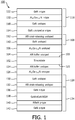
- Fig. 1 is a cross-sectional view of an epitaxial structure 100 for integrating GaN LEDs with AlGaN/GaN devices on a silicon (Si) substrate 102 in one or more embodiments of the present disclosure.
- GaN is not well suited for direct epitaxial growth on Si substrates due to the fact that Ga and Si form an eutectic material that destroys the Si substrate
- an undoped aluminum nitride (A1N) buffer layer 104 is first formed over a first side 105 of silicon substrate 102 (e.g., a topside as shown) to serve as a barrier between GaN and silicon.
- a thin AlN buffer layer 104 e.g., 100 angstroms to 2 microns
- An undoped Al x Ga 1-x N layer 106 may be formed over undoped AlN buffer layer 104 to provide additional separation between Si and GaN.
- a strain engineered stack 108 may be formed over Al x Ga 1-x N layer 106. Strain engineered stack 108 accommodates the strain due to a thermal expansion difference between Si and GaN in structure 100. Strain engineered stack 108 includes an undoped or doped GaN layer 110 and an undoped or doped AlN strain-releasing layer 112 over GaN layer 110. GaN layer 110 of stack 108 is formed directly over Al x Ga 1-x N layer 106. A second strain engineered stack 108A (not shown) maybe formed over first engineered stack 108.
- GaN layer 114 is formed over AlN strain-releasing layer 112 of strain engineered stack 108 to separate strain engineered stack 108 from an AlGaN/GaN heterojunction stack 116.
- GaN layer 114 may be doped with n-type dopant such as iron (Fe) to increase its resistance.
- GaN layer 114 is a non-conducting layer which prevents lateral leakage current from any HFET formed in an AlGaN/GaN heterojunction stack 116 (described later) above GaN layer 114 when the HFET is turned off. Isolation trenches may be etched down to GaN layer 114 to electrically insulate devices formed above GaN layer 114.
- AlGaN/GaN heterojunction stack 116 is formed over GaN layer 114.
- AlGaN/GaN heterojunction stack 116 includes an undoped GaN layer 118, a heavily doped, n-type Al x Ga 1-x N layer 120 on undoped GaN layer 118, and a passivation layer 122 (e.g., an n-type GaN) over n-type Al x Ga 1-x N layer 120.
- Undoped GaN layer 118 of heterojunction stack 116 is directly over GaN layer 114.
- AlGaN/GaN heterojunction stack 116 may be further processed to form devices including HFETs and Schottky diodes.
- Additional circuit elements may be integrated with, or built in layers over, AlGaN/GaN heterojunction stack 116.
- a resistor may be made utilizing a semiconductor layer of AlGaN/GaN heterojunction stack 116 (e.g., GaN layer 118) by forming two metal contacts at a certain distance between them.
- a capacitor may be made of a dielectric layer (silicon dioxide or silicon nitride) deposited above AlGaN/GaN heterojunction stack 116 and sandwiched between two metal layers, and an inductor may be made by forming a long winding metal pattern atop a semiconductor layer of AlGaN/GaN heterojunction stack 116 (e.g., GaN layer 118).
- An undoped AlN buffer layer 124 is formed over a second side 125 of silicon substrate 102 to serve as a barrier layer between GaN and silicon.
- An undoped Al x Ga 1-x N layer 126 is formed over undoped AlN buffer layer 124 to provide stress relief due to difference in thermal expansion and lattice constants between GaN and Si.
- a strain engineered stack 128 may be formed over undoped Al x Ga 1-x N layer 126. Strain engineered stack 128 includes an undoped GaN layer 130 and an undoped AlN strain-releasing layer 132 over undoped GaN layer 130. Undoped GaN layer 130 of stack 128 is directly over Al x Ga 1-x N layer 126. The structure of strain engineered stack 128 may be repeated over another engineered stack 128.
- GaN LED stack 134 is formed over undoped AlN strain-releasing layer 132 of strain engineering stack 128.
- GaN LED stack 134 includes an n-type GaN layer 136, GaN/ In y Ga 1-y N multiple quantum well (MQW) layers 138 over n-type GaN layer 136, a p-type Al x Ga 1-x N layer 140 over GaN/ In y Ga 1-y N MQW layers 138, and a p-type GaN layer 142 over p-type Al x Ga 1-x N layer 140.
- MQW multiple quantum well
- Al x Ga 1-x N and In y Ga 1-y N in different layers may be of different compositions and may be generally indicated as AlGaN and InGaN, respectively.
- N-type GaN layer 136 of stack 134 is directly over undoped AlN strain-releasing layer 132.
- GaN LED stack 134 may be further processed to exposed areas of n-type GaN layer 136 and p-type GaN layer 142 for forming n- and p-contacts. Additional circuit elements may be integrated with, or built in layers over, GaN LED stack 134.
- GaN LED stack 134 is not formed over a non-conducting GaN layer like heterojunction stack 116 because LEDs are vertical devices so lateral leakage current is not of great concern.
- Fig. 2 is a cross-sectional view of an epitaxial structure 200 for integrating GaN LEDs with AlGaN/GaN devices on a sapphire substrate 202 in one or more embodiments of the present disclosure.
- An undoped buffer layer 204 is first formed over a first side 205 of sapphire substrate 202 (e.g., a topside as shown) to provide a seed for growing other layers.
- Undoped buffer layer 204 maybe composed of GaN or AIN.
- An undoped GaN layer 206 is next formed on undoped buffer layer 204.
- GaN layer 206 maybe doped with n-type dopant such as Fe to increase its resistance.
- GaN layer 206 is non-conducting so it prevents lateral leakage current from any HFET device above the layer when the HFET is turned off. Isolation trenches may be etched down to GaN layer 206 to electrically insulate devices formed above the layer.
- AlGaN/GaN heterojunction stack 116 (described earlier) is formed over GaN layer 206. Undoped GaN layer 118 of heterojunction stack 116 is directly over GaN layer 206. AlGaN/GaN heterojunction stack 116 may be further processed to form devices including HFETs and Schottky diodes. Additional circuit elements may be integrated with, or built in layers over, AlGaN/GaN heterojunction stack 116.
- Undoped nucleation layer 208 is formed over a second side 209 of sapphire substrate 202 (e.g., a backside as shown) to seed other layers.
- Undoped nucleation layer 208 may be composed of GaN or AlN.
- GaN LED stack 134 (described earlier) is formed over undoped nucleation layer 208.
- N-type GaN layer 136 of stack 134 is directly over undoped nucleation layer 208.
- GaN LED stack 134 may be further processed to exposed areas of n-type GaN layer 136 and p-type GaN layer 142 for forming n- and p-contacts. Additional circuit elements may be integrated with, or built in layers over, GaN LED stack 134.
- Fig. 3 is a cross-sectional view of an epitaxial structure 300 for integrating GaN LEDs with AlGaN/GaN devices on a silicon carbon (SiC) substrate 302 in one or more embodiments of the present disclosure.
- An undoped nucleation layer 304 is first formed over a first side 305 of SiC substrate 302 (e.g., a topside as shown) to seed other layers.
- Undoped nucleation layer 304 may be composed of AlN or Al x Ga 1-x N.
- An undoped GaN layer 306 is next formed on undoped nucleation layer 304.
- GaN layer 306 maybe doped with n-type dopant such Fe to increase its resistance.
- GaN layer 306 is non-conducting so it prevents lateral leakage current from any HFET device above the layer when the HFET is turned off. Isolation trenches may be etched down to GaN layer 306 to electrically insulate devices formed above the layer.
- AlGaN/GaN heterojunction stack 116 (described earlier) is formed over GaN layer 306. Undoped GaN layer 118 of heterojunction stack 116 is directly over GaN layer 306. AlGaN/GaN heterojunction stack 116 may be further processed to form devices including HFETs and Schottky diodes. Additional circuit elements may be integrated with, or built in layers over, AlGaN/GaN heterojunction stack 116.
- Undoped nucleation layer 308 is formed over a second side (e.g., a backside as shown) 309 of SiC substrate 302 to seed other layers.
- Undoped nucleation layer 308 may be composed of AlN or Al x Ga 1-x N.
- GaN LED stack 134 (described earlier) is formed over undoped nucleation layer 308.
- N-type GaN layer 136 of stack 134 is directly over undoped nucleation layer 308.
- GaN LED stack 134 may be further processed to expose areas of n-type GaN layer 136 and p-type GaN layer 142 for forming n- and p-contacts. Additional circuit elements may be integrated with, or built in layers over, GaN LED stack 134.
- Fig. 4 is a cross-sectional view of an epitaxial structure 400 for integrating GaN LEDs with AlGaN/GaN devices on a GaN substrate 402 in one or more embodiments of the present disclosure.
- An undoped GaN layer 404 may be formed on a first side 405 of GaN substrate 402 (e.g., a topside as shown).
- GaN layer 404 maybe doped with n-type dopant such Fe to increase its resistance.
- GaN layer 404 is non-conducting so it prevents lateral leakage current from any HFET device above the layer when the HFET is turned off. Isolation trenches may be etched down to GaN layer 404 to electrically insulate devices formed above the layer.
- AlGaN/GaN heterojunction stack 116 (described earlier) is formed over GaN layer 404. Undoped GaN layer 118 of heterojunction stack 116 is directly over GaN layer 404. AlGaN/GaN heterojunction stack 116 may be further processed to form devices including HFETs and Schottky diodes. Additional circuit elements may be integrated with, or built in layers over, AlGaN/GaN heterojunction stack 116.
- GaN LED stack 134 (described earlier) is formed on a second side 406 of GaN substrate 402 (e.g., a backside as shown). N-type GaN layer 136 of stack 134 is directly over GaN substrate 402. GaN LED stack 134 may be further processed to exposed areas of n-type GaN layer 136 and p-type GaN layer 142 for forming n- and p-contacts. Additional circuit elements may be integrated with, or built in layers over, GaN LED stack 134.
- Fig. 5 shows a cross-sectional view of a structure 500 resulting from structure 200 ( Fig. 2 ) undergoing additional processing to form an AlGaN/GaN HFETs 506 and an AlGaN/GaN Schottky diode 508 in one or more embodiments of the present disclosure.
- P-type GaN layer 142 in GaN LED stack 134 may be roughened to improve light extraction.
- a p-contact 501 is formed on p-type GaN layer 142.
- One or more portions of structure 200 are removed down into n-type GaN layer 136 to form an n-contact 502 for an LED in GaN LED stack 134.
- portion of layers 116, 206, 204, 202, and 208 may be removed to form n-contact 502.
- layers 206, 204 202, 208, and all layers of GaN LED stack 134 except p-type GaN layer 142 may be removed to form p-contact 501. Locating all contacts on one side of the device enables a flip-chip configuration.
- An isolation trench 504 is etched through AlGaN/GaN heterojunction stack 116, GaN layer 206, and GaN or AlN buffer layer 204 down to sapphire substrate 202 to electrically insulate an HFET 506 and a Schottky diode 508.
- HFET 506 and Schottky diode 508 are connected by interconnects (not shown) to form a driver circuit for the LED in GaN LED stack 134.
- Other circuit elements such as resistors, capacitors, and inductors may also be formed in AlGaN/GaN heterojunction stack 116.
- HFET 506 includes a gate 512 and a source 514 and a drain 516 on the opposite sides of gate 512.
- Gate 512 contacts n-type Al x Ga 1-x N layer 120, and source 514 and drain 516 contact undoped GaN layer 118.
- an opening is etched in n-type GaN passivation layer 122 and metal is deposited on n-type Al x Ga 1-x N layer 120.
- metal is deposited on n-type GaN passivation layer 122 and diffused down to undoped GaN layer 118 by annealing.
- Schottky diode 508 includes an anode electrode 518 and a cathode electrode 520.
- Anode electrode 518 contacts n-type Al x Ga 1-x N layer 120.
- an opening is etched in n-type GaN passivation layer 122 and metal is deposited on n-type Al x Ga 1-x N layer 120.
- Cathode electrode 520 contacts undoped GaN layer 118.
- metal is deposited on n-type GaN passivation layer 122 and diffused down to undoped GaN layer 118 by annealing.
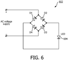
- Fig. 6 is a circuit diagram of a bridge rectifier circuit 602 connected to an LED 604.
- Bridge rectifier circuit 602 converts an AC voltage supply to DC voltage in order to power the LED in one or more embodiments of the present disclosure.
- Circuit 602 includes diodes D1, D2, D3, and D4 arranged in a typical diamond configuration where the cathode of diode D1 is connected to the anode of diode D2 and one side of the AC supply voltage, the cathode of diode D4 is connected to the anode of diode D3 and the other side of the AC supply voltage.
- the anodes of diodes D1 and D4 are the negative side of the rectified supply voltage for LED 604 and are connected to the cathode of LED 604.
- the cathodes of diodes D2 and D3 are the positive side of the rectified voltage and are connected to the anode of LED 604.
- Fig. 7 shows a cross-sectional view of a structure 700 resulting from structure 200 ( Fig. 2 ) undergoing additional processing to form bridge rectifier circuit 602 ( Fig. 6 ) in one or more embodiments of the present disclosure.
- Each diode in circuit 602 is implemented as an AlGaN/GaN Schottky diode in heterojunction stack 116.
- Diode D1 includes an anode electrode 702 and a cathode electrode 704.
- Diode D2 has an anode electrode 706 and shares a cathode electrode 708 with diode D3 because they are connected in series through undoped GaN layer 118.
- Diode D3 has an anode electrode 710 and cathode electrode 708.
- Diode D4 has an anode electrode 712 and a cathode electrode 714. Each anode electrode contacts n-type Al x Ga 1-x N layer 120, and each cathode electrode contacts undoped GaN layer 118. Diodes D1, D2, D3, and D4 are formed by the method described for forming diode 508 in structure 500 ( Fig. 5 ).
- Portions of AlGaN/GaN heterojunction stack 116, GaN layer 206, and GaN or AlN buffer layer 204 are removed to expose areas of sapphire substrate 202.
- an n-contact 722 is formed by etching an opening through sapphire substrate 202 and GaN or AlN buffer layer 208 and partially into n-type GaN layer 136 in GaN LED stack 134, and depositing metal in the opening.
- a p-contact 726 is formed by etching a hole through sapphire substrate 202, GaN or AlN buffer layer 208, and GaN LED stack 134, and depositing metal in the hole to contact p-type GaN layer 142 in GaN LED stack 134.
- the sidewalls of the holes for n-contact 722 and p-contact 726 are covered with an insulator such an oxide.
- the openings for n-contact 722 and p-contact 726 are each wide enough to allow a pillar of metal to be deposited without contacting the "sides" of the opening.
- a portion of p-type GaN layer 142 is left at the bottom of the opening and p-contact is 726 is deposited on the non-roughened surface of p-type GaN layer 142.
- Diodes D1, diodes D2, D3, and diodes D4 are electrically insulated from each other by isolation trenches 716.
- Isolation trenches 716 are etched through AlGaN/GaN heterojunction stack 116, GaN layer 206, and GaN or AlN buffer layer 204 down to sapphire substrate 202 to electrically insulate diodes D1, the pair of diodes D2, D3, and D4 from each other.
- Interconnects connect diodes D1, D2, D3, and D4 as shown in Fig. 6 .
- interconnects connect cathode electrode 708 (the cathodes of D2 and D3) to p-contact 726, the anode, of the LED in GaN LED stack 126, and anode electrodes 702 and 712 to n-contact 722, the cathode, of the LED in GaN LED stack 134.
- One side of the AC voltage is supplied to cathode electrode 704 of diode D1 and also to anode electrode 706 of diode D2.
- the other side of the AC voltage is supplied to anode electrode 710 of diode D3 and also to cathode electrode 714 of diode D4.
- Embodiments of the present disclosure offer the following advantages over the conventional LED-based light fixtures.
- the embodiments of the present disclosure integrate LEDs with the LED driver circuit on the same substrate template. Devices will be integrated on wafer-level with metal interconnects instead of the conventional method of making discrete LEDs and the LED driver circuit separately and then combining them at the die level.
- GaN transistor switches have lower specific-on-resistance than Si-based devices, providing less ohmic losses due to switching.
- the embodiments of the present disclosure have a smaller footprint.
- GaN transistors can handle higher operating voltage than Si-based devices so switching transistors can be made smaller.
- Necessary capacitors or inductors can also be made on wafer levels, thus reducing overall area.
- Die level interconnect such as wire bonding and soldering, is no longer needed between the LED driver circuit and LEDs as they are now done at wafer level.
- the embodiments of the present disclosure provide better temperature stability and prevent thermal runaway.
- LED current tends to have a positive temperature coefficient when driven at constant voltage because the LED's turn-on voltage becomes smaller when the LED warms up.
- FET field-effect transistor
- a field-effect transistor FET
- the embodiments of the present disclosure allow easier manufacturing for LED companies.
- An LED company may procure epitaxial wafers with AlGaN/GaN transistor structures grown on Si, sapphire, or SiC substrates from other companies and focus on improving LED structures on the other side of the substrates without worrying about optimizing the transistor structures.
- the thickness of the LED structures would not interfere with the transistor structures grown on the other side of the substrates. In other words, wafer processing of LEDs and transistors would not severely impact each other.
Landscapes
- Led Devices (AREA)
- Junction Field-Effect Transistors (AREA)
- Electrodes Of Semiconductors (AREA)
Description
- The present disclosure relates to semiconductor light emitting diodes, and more particular to gallium nitride light emitting diodes with aluminum gallium nitride/gallium nitride devices on a substrate.
- A light emitting diode (LED) is a direct current (DC) device that needs a constant voltage supply. However, a LED-based light fixture runs from a mains supply of alternating voltage (AC). As a result, the LED-based light fixture includes a LED driver that is able to handle large AC and convert it to DC voltage. The LED driver is usually made of silicon devices such as laterally diffused metal oxide semiconductors (LDMOS) or power metal-oxide-semiconductor field-effect transistors (MOSFETs).
- Prior art documents
WO2011079645 A1 andJP2002305327 A - Prior art documents
JP2000036639 A JP2003086784 A - Present invention describes a method for fabricating an epitaxial structure, according to the
independent claim 1, and a corresponding epitaxial structure according to the independent claim 9. Further preferred embodiments are defined in the dependent claims. - In the drawings:
-
FIG. 1 is a cross-sectional view of an epitaxial structure for integrating gallium nitride (GaN) light emitting diodes (LEDs) with aluminum gallium nitride(A1GaN)/GaN devices on a silicon substrate; -
FIG. 2 is a cross-sectional view of an epitaxial structure for integrating GaN LEDs with AlGaN/GaN devices on a sapphire substrate; -
FIG. 3 is a cross-sectional view of an epitaxial structure for integrating GaN LEDs with AlGaN/GaN devices on a silicon carbon (SiC) substrate; -
FIG. 4 is a cross-sectional view of an epitaxial structure for integrating GaN LEDs with AlGaN/GaN devices on a GaN substrate; -
Fig. 5 shows a cross-sectional view of a structure resulting from the structure ofFig. 2 undergoing additional processing to form an AlGaN/GaN heterojunction field-effect transistor (HFET) and an AlGaN/GaN Schottky diode; -
Fig. 6 is a circuit diagram of a bridge rectifier circuit connected in series with an LED; and -
Fig. 7 shows a cross-sectional view of a structure resulting from the structure ofFig. 2 undergoing additional processing to form the bridge rectifier circuit ofFig. 6 , all arranged in accordance with embodiments of the invention. - Use of the same reference numbers in different figures indicates similar or identical elements.
- As gallium nitride (GaN) has a higher band gap than silicon (Si), GaN transistors have a much higher breakdown voltage than Si transistors so GaN transistors can handle much higher voltage and current density. This allows smaller GaN transistors to handle the same voltage as larger Si-based power transistors. With the advent of GaN-on-Si technology, GaN transistors grown on 150 mm (6-inch) silicon substrates are price-competitive with silicon-based power devices and offer better performance. By integrating GaN light emitting diodes (LEDs) with GaN transistors on silicon substrates, the combined architecture will be more economical and have higher AC-DC conversion efficiency than the conventional approach that pairs GaN LEDs with a discrete Si-based electric driver.
- In accordance with embodiments of the present disclosure, an epitaxial structure is made by forming GaN LEDs on one side of a substrate and forming aluminum gallium nitride (AlGaN)/GaN devices (or vice versa) on the other side of the substrate. The AlGaN/GaN devices may be heterojunction field-effect transistors (HFETs) and Schottky diodes used for AC-DC conversion or DC-DC down conversion (high-voltage to low-voltage conversion). Several LEDs and the AlGaN/GaN devices may be connected in series or in parallel depending on the conversion scheme.
- Note the use of "over" includes forming one layer or a stack of layers directly on another layer or stack of layers. Depending on if a structure is located on a top or backside of a substrate, "over" may indicate one layer or a stack of layers above or below another layer or stack of layers, respectively. The term stack or stack of layers may be used interchangeably.
-
Fig. 1 is a cross-sectional view of anepitaxial structure 100 for integrating GaN LEDs with AlGaN/GaN devices on a silicon (Si)substrate 102 in one or more embodiments of the present disclosure. As GaN is not well suited for direct epitaxial growth on Si substrates due to the fact that Ga and Si form an eutectic material that destroys the Si substrate, an undoped aluminum nitride (A1N)buffer layer 104 is first formed over afirst side 105 of silicon substrate 102 (e.g., a topside as shown) to serve as a barrier between GaN and silicon. A thin AlN buffer layer 104 (e.g., 100 angstroms to 2 microns) is used to reduce defect density. An undoped AlxGa1-xN layer 106 may be formed over undopedAlN buffer layer 104 to provide additional separation between Si and GaN. - A strain engineered
stack 108 may be formed over AlxGa1-xNlayer 106. Strain engineeredstack 108 accommodates the strain due to a thermal expansion difference between Si and GaN instructure 100. Strain engineeredstack 108 includes an undoped or doped GaNlayer 110 and an undoped or doped AlN strain-releasinglayer 112 over GaNlayer 110. GaNlayer 110 ofstack 108 is formed directly over AlxGa1-xNlayer 106. A second strain engineered stack 108A (not shown) maybe formed over first engineeredstack 108. - An undoped GaN
layer 114 is formed over AlN strain-releasinglayer 112 of strain engineeredstack 108 to separate strain engineeredstack 108 from an AlGaN/GaN heterojunction stack 116. Alternatively GaNlayer 114 may be doped with n-type dopant such as iron (Fe) to increase its resistance. GaNlayer 114 is a non-conducting layer which prevents lateral leakage current from any HFET formed in an AlGaN/GaN heterojunction stack 116 (described later) aboveGaN layer 114 when the HFET is turned off. Isolation trenches may be etched down to GaNlayer 114 to electrically insulate devices formed aboveGaN layer 114. - AlGaN/GaN
heterojunction stack 116 is formed over GaNlayer 114. AlGaN/GaNheterojunction stack 116 includes anundoped GaN layer 118, a heavily doped, n-type AlxGa1-xN layer 120 on undopedGaN layer 118, and a passivation layer 122 (e.g., an n-type GaN) over n-type AlxGa1-xN layer 120. Undoped GaNlayer 118 ofheterojunction stack 116 is directly over GaNlayer 114. AlGaN/GaN heterojunction stack 116 may be further processed to form devices including HFETs and Schottky diodes. Additional circuit elements may be integrated with, or built in layers over, AlGaN/GaNheterojunction stack 116. For example, a resistor may be made utilizing a semiconductor layer of AlGaN/GaN heterojunction stack 116 (e.g., GaN layer 118) by forming two metal contacts at a certain distance between them. Also, a capacitor may be made of a dielectric layer (silicon dioxide or silicon nitride) deposited above AlGaN/GaN heterojunction stack 116 and sandwiched between two metal layers, and an inductor may be made by forming a long winding metal pattern atop a semiconductor layer of AlGaN/GaN heterojunction stack 116 (e.g., GaN layer 118). - An undoped
AlN buffer layer 124 is formed over asecond side 125 ofsilicon substrate 102 to serve as a barrier layer between GaN and silicon. An undoped AlxGa1-xNlayer 126 is formed over undopedAlN buffer layer 124 to provide stress relief due to difference in thermal expansion and lattice constants between GaN and Si. - A strain engineered
stack 128 may be formed over undoped AlxGa1-xNlayer 126. Strain engineeredstack 128 includes an undoped GaNlayer 130 and an undoped AlN strain-releasinglayer 132 over undoped GaNlayer 130. Undoped GaNlayer 130 ofstack 128 is directly over AlxGa1-xNlayer 126. The structure of strain engineeredstack 128 may be repeated over another engineeredstack 128. - A GaN
LED stack 134 is formed over undoped AlN strain-releasinglayer 132 ofstrain engineering stack 128. GaNLED stack 134 includes an n-type GaN layer 136, GaN/ InyGa1-yN multiple quantum well (MQW)layers 138 over n-type GaN layer 136, a p-type AlxGa1-xN layer 140 over GaN/ InyGa1-yN MQW layers 138, and a p-type GaN layer 142 over p-type AlxGa1-xN layer 140. Note that AlxGa1-xN and InyGa1-yN in different layers may be of different compositions and may be generally indicated as AlGaN and InGaN, respectively. N-type GaN layer 136 ofstack 134 is directly over undoped AlN strain-releasinglayer 132. GaNLED stack 134 may be further processed to exposed areas of n-type GaN layer 136 and p-type GaN layer 142 for forming n- and p-contacts. Additional circuit elements may be integrated with, or built in layers over, GaNLED stack 134. - Note that
GaN LED stack 134 is not formed over a non-conducting GaN layer likeheterojunction stack 116 because LEDs are vertical devices so lateral leakage current is not of great concern. -
Fig. 2 is a cross-sectional view of anepitaxial structure 200 for integrating GaN LEDs with AlGaN/GaN devices on asapphire substrate 202 in one or more embodiments of the present disclosure. Anundoped buffer layer 204 is first formed over afirst side 205 of sapphire substrate 202 (e.g., a topside as shown) to provide a seed for growing other layers.Undoped buffer layer 204 maybe composed of GaN or AIN. Anundoped GaN layer 206 is next formed onundoped buffer layer 204. AlternativelyGaN layer 206 maybe doped with n-type dopant such as Fe to increase its resistance.GaN layer 206 is non-conducting so it prevents lateral leakage current from any HFET device above the layer when the HFET is turned off. Isolation trenches may be etched down toGaN layer 206 to electrically insulate devices formed above the layer. - AlGaN/GaN heterojunction stack 116 (described earlier) is formed over
GaN layer 206.Undoped GaN layer 118 ofheterojunction stack 116 is directly overGaN layer 206. AlGaN/GaN heterojunction stack 116 may be further processed to form devices including HFETs and Schottky diodes. Additional circuit elements may be integrated with, or built in layers over, AlGaN/GaN heterojunction stack 116. - An
undoped nucleation layer 208 is formed over asecond side 209 of sapphire substrate 202 (e.g., a backside as shown) to seed other layers.Undoped nucleation layer 208 may be composed of GaN or AlN. GaN LED stack 134 (described earlier) is formed overundoped nucleation layer 208. N-type GaN layer 136 ofstack 134 is directly overundoped nucleation layer 208.GaN LED stack 134 may be further processed to exposed areas of n-type GaN layer 136 and p-type GaN layer 142 for forming n- and p-contacts. Additional circuit elements may be integrated with, or built in layers over,GaN LED stack 134. -
Fig. 3 is a cross-sectional view of anepitaxial structure 300 for integrating GaN LEDs with AlGaN/GaN devices on a silicon carbon (SiC)substrate 302 in one or more embodiments of the present disclosure. Anundoped nucleation layer 304 is first formed over afirst side 305 of SiC substrate 302 (e.g., a topside as shown) to seed other layers.Undoped nucleation layer 304 may be composed of AlN or AlxGa1-xN. Anundoped GaN layer 306 is next formed onundoped nucleation layer 304. AlternativelyGaN layer 306 maybe doped with n-type dopant such Fe to increase its resistance.GaN layer 306 is non-conducting so it prevents lateral leakage current from any HFET device above the layer when the HFET is turned off. Isolation trenches may be etched down toGaN layer 306 to electrically insulate devices formed above the layer. - AlGaN/GaN heterojunction stack 116 (described earlier) is formed over
GaN layer 306.Undoped GaN layer 118 ofheterojunction stack 116 is directly overGaN layer 306. AlGaN/GaN heterojunction stack 116 may be further processed to form devices including HFETs and Schottky diodes. Additional circuit elements may be integrated with, or built in layers over, AlGaN/GaN heterojunction stack 116. - An
undoped nucleation layer 308 is formed over a second side (e.g., a backside as shown) 309 ofSiC substrate 302 to seed other layers.Undoped nucleation layer 308 may be composed of AlN or AlxGa1-xN. GaN LED stack 134 (described earlier) is formed overundoped nucleation layer 308. N-type GaN layer 136 ofstack 134 is directly overundoped nucleation layer 308.GaN LED stack 134 may be further processed to expose areas of n-type GaN layer 136 and p-type GaN layer 142 for forming n- and p-contacts. Additional circuit elements may be integrated with, or built in layers over,GaN LED stack 134. -
Fig. 4 is a cross-sectional view of anepitaxial structure 400 for integrating GaN LEDs with AlGaN/GaN devices on aGaN substrate 402 in one or more embodiments of the present disclosure. Anundoped GaN layer 404 may be formed on afirst side 405 of GaN substrate 402 (e.g., a topside as shown). AlternativelyGaN layer 404 maybe doped with n-type dopant such Fe to increase its resistance.GaN layer 404 is non-conducting so it prevents lateral leakage current from any HFET device above the layer when the HFET is turned off. Isolation trenches may be etched down toGaN layer 404 to electrically insulate devices formed above the layer. - AlGaN/GaN heterojunction stack 116 (described earlier) is formed over
GaN layer 404.Undoped GaN layer 118 ofheterojunction stack 116 is directly overGaN layer 404. AlGaN/GaN heterojunction stack 116 may be further processed to form devices including HFETs and Schottky diodes. Additional circuit elements may be integrated with, or built in layers over, AlGaN/GaN heterojunction stack 116. - GaN LED stack 134 (described earlier) is formed on a
second side 406 of GaN substrate 402 (e.g., a backside as shown). N-type GaN layer 136 ofstack 134 is directly overGaN substrate 402.GaN LED stack 134 may be further processed to exposed areas of n-type GaN layer 136 and p-type GaN layer 142 for forming n- and p-contacts. Additional circuit elements may be integrated with, or built in layers over,GaN LED stack 134. -
Fig. 5 shows a cross-sectional view of astructure 500 resulting from structure 200 (Fig. 2 ) undergoing additional processing to form an AlGaN/GaN HFETs 506 and an AlGaN/GaN Schottky diode 508 in one or more embodiments of the present disclosure. - P-
type GaN layer 142 inGaN LED stack 134 may be roughened to improve light extraction. A p-contact 501 is formed on p-type GaN layer 142. One or more portions of structure 200 (Fig. 2 ) are removed down into n-type GaN layer 136 to form an n-contact 502 for an LED inGaN LED stack 134. In the alternative, portion oflayers contact 502. In yet another alternative, layers 206, 204 202, 208, and all layers ofGaN LED stack 134 except p-type GaN layer 142 may be removed to form p-contact 501. Locating all contacts on one side of the device enables a flip-chip configuration. - An
isolation trench 504 is etched through AlGaN/GaN heterojunction stack 116,GaN layer 206, and GaN orAlN buffer layer 204 down tosapphire substrate 202 to electrically insulate anHFET 506 and aSchottky diode 508.HFET 506 andSchottky diode 508 are connected by interconnects (not shown) to form a driver circuit for the LED inGaN LED stack 134. Other circuit elements such as resistors, capacitors, and inductors may also be formed in AlGaN/GaN heterojunction stack 116. -
HFET 506 includes agate 512 and asource 514 and adrain 516 on the opposite sides ofgate 512.Gate 512 contacts n-type AlxGa1-xN layer 120, andsource 514 and drain 516 contactundoped GaN layer 118. Forgate 512, an opening is etched in n-typeGaN passivation layer 122 and metal is deposited on n-type AlxGa1-xN layer 120. Forsource 514 and drain 516, metal is deposited on n-typeGaN passivation layer 122 and diffused down toundoped GaN layer 118 by annealing. -
Schottky diode 508 includes ananode electrode 518 and acathode electrode 520.Anode electrode 518 contacts n-type AlxGa1-xN layer 120. Toform anode electrode 518, an opening is etched in n-typeGaN passivation layer 122 and metal is deposited on n-type AlxGa1-xN layer 120.Cathode electrode 520 contactsundoped GaN layer 118. To formcathode electrode 520, metal is deposited on n-typeGaN passivation layer 122 and diffused down toundoped GaN layer 118 by annealing. -
Fig. 6 is a circuit diagram of abridge rectifier circuit 602 connected to anLED 604.Bridge rectifier circuit 602 converts an AC voltage supply to DC voltage in order to power the LED in one or more embodiments of the present disclosure.Circuit 602 includes diodes D1, D2, D3, and D4 arranged in a typical diamond configuration where the cathode of diode D1 is connected to the anode of diode D2 and one side of the AC supply voltage, the cathode of diode D4 is connected to the anode of diode D3 and the other side of the AC supply voltage. The anodes of diodes D1 and D4 are the negative side of the rectified supply voltage forLED 604 and are connected to the cathode ofLED 604. The cathodes of diodes D2 and D3 are the positive side of the rectified voltage and are connected to the anode ofLED 604. -
Fig. 7 shows a cross-sectional view of astructure 700 resulting from structure 200 (Fig. 2 ) undergoing additional processing to form bridge rectifier circuit 602 (Fig. 6 ) in one or more embodiments of the present disclosure. Each diode incircuit 602 is implemented as an AlGaN/GaN Schottky diode inheterojunction stack 116. Diode D1 includes ananode electrode 702 and acathode electrode 704. Diode D2 has ananode electrode 706 and shares acathode electrode 708 with diode D3 because they are connected in series throughundoped GaN layer 118. Diode D3 has ananode electrode 710 andcathode electrode 708. Diode D4 has ananode electrode 712 and acathode electrode 714. Each anode electrode contacts n-type AlxGa1-xN layer 120, and each cathode electrode contacts undopedGaN layer 118. Diodes D1, D2, D3, and D4 are formed by the method described for formingdiode 508 in structure 500 (Fig. 5 ). - Portions of AlGaN/
GaN heterojunction stack 116,GaN layer 206, and GaN orAlN buffer layer 204 are removed to expose areas ofsapphire substrate 202. In one exposed area, an n-contact 722 is formed by etching an opening throughsapphire substrate 202 and GaN orAlN buffer layer 208 and partially into n-type GaN layer 136 inGaN LED stack 134, and depositing metal in the opening. In another exposed area, a p-contact 726 is formed by etching a hole throughsapphire substrate 202, GaN orAlN buffer layer 208, andGaN LED stack 134, and depositing metal in the hole to contact p-type GaN layer 142 inGaN LED stack 134. Although not shown, the sidewalls of the holes for n-contact 722 and p-contact 726 are covered with an insulator such an oxide. In an alternative embodiment the openings for n-contact 722 and p-contact 726 are each wide enough to allow a pillar of metal to be deposited without contacting the "sides" of the opening. In another alternative a portion of p-type GaN layer 142 is left at the bottom of the opening and p-contact is 726 is deposited on the non-roughened surface of p-type GaN layer 142. In this last embodiment there is no p-contact blocking any of the light from the LED formed byGaN LED stack 134. - Diodes D1, diodes D2, D3, and diodes D4 are electrically insulated from each other by
isolation trenches 716.Isolation trenches 716 are etched through AlGaN/GaN heterojunction stack 116,GaN layer 206, and GaN orAlN buffer layer 204 down tosapphire substrate 202 to electrically insulate diodes D1, the pair of diodes D2, D3, and D4 from each other. Interconnects connect diodes D1, D2, D3, and D4 as shown inFig. 6 . In particular, interconnects connect cathode electrode 708 (the cathodes of D2 and D3) to p-contact 726, the anode, of the LED inGaN LED stack 126, andanode electrodes contact 722, the cathode, of the LED inGaN LED stack 134. One side of the AC voltage is supplied tocathode electrode 704 of diode D1 and also toanode electrode 706 of diode D2. The other side of the AC voltage is supplied toanode electrode 710 of diode D3 and also tocathode electrode 714 of diode D4. - Embodiments of the present disclosure offer the following advantages over the conventional LED-based light fixtures. The embodiments of the present disclosure integrate LEDs with the LED driver circuit on the same substrate template. Devices will be integrated on wafer-level with metal interconnects instead of the conventional method of making discrete LEDs and the LED driver circuit separately and then combining them at the die level.
- The embodiments of the present disclosure improve AC-DC conversion efficiency. GaN transistor switches have lower specific-on-resistance than Si-based devices, providing less ohmic losses due to switching.
- The embodiments of the present disclosure have a smaller footprint. GaN transistors can handle higher operating voltage than Si-based devices so switching transistors can be made smaller. Necessary capacitors or inductors can also be made on wafer levels, thus reducing overall area.
- The embodiments of the present disclosure are more economical. Die level interconnect, such as wire bonding and soldering, is no longer needed between the LED driver circuit and LEDs as they are now done at wafer level.
- The embodiments of the present disclosure provide better temperature stability and prevent thermal runaway. LED current tends to have a positive temperature coefficient when driven at constant voltage because the LED's turn-on voltage becomes smaller when the LED warms up. In contrast, a field-effect transistor (FET) tends to have negative temperature coefficient due to drop in carrier mobility as the FET warms up. By placing LEDs and the LED driver circuit on the same substrate, the temperature effect is self-compensated, thereby preventing thermal runaway.
- The embodiments of the present disclosure allow easier manufacturing for LED companies. An LED company may procure epitaxial wafers with AlGaN/GaN transistor structures grown on Si, sapphire, or SiC substrates from other companies and focus on improving LED structures on the other side of the substrates without worrying about optimizing the transistor structures. Furthermore, the thickness of the LED structures would not interfere with the transistor structures grown on the other side of the substrates. In other words, wafer processing of LEDs and transistors would not severely impact each other.
- Various other adaptations and combinations of features of the embodiments disclosed are possible within the scope of the invention as defined in the appended claims. Numerous embodiments are encompassed by the following claims.
Claims (15)
- A method for fabricating an epitaxial structure, comprising:providing a substrate (102,202,302,402) and a heterojunction stack (116) over a first side (105,205,305,405) of the substrate, the heterojunction stack comprising an undoped gallium nitride, GaN, layer (118) over the first side of the substrate and a doped aluminum gallium nitride, AlGaN, layer (120) on the undoped GaN layer;forming a GaN light emitting diode stack (134) over a second side (125,209,309,406) of the substrate, the GaN light emitting diode stack comprising an n-type GaN layer (136) over the second side of the substrate, a GaN/indium gallium nitride, InGaN, multiple quantum well, MQW, structure (138) over the n-type GaN layer, a p-type AlGaN layer (140) over the n-type GaN/InGaN MQW structure, and a p-type GaN layer (142) over the p-type AlGaN layer,and further processing the heterojunction stack to form one or more devices electrically coupled to the light emitting diode stack, to form a driver circuit, the one or more devices including one or more of an AlGaN/GaN heterojunction field effect transistor, HFET, (506) and an AlGaN/GaN Schottky diode (508).
- The method of claim 1, wherein:the substrate is a silicon substrate (102);providing the substrate and the heterojunction stack over the first side (105) of the substrate comprises:forming a first strain engineered stack (108) over the first side of the substrate, the first strain engineered stack accommodating strain between silicon and GaN; andforming the heterojunction stack over the first strain engineered stack; andthe method further comprises forming a second strain engineered stack (128) over the second side (125) of the substrate, the GaN light emitting diode stack (134) being formed over the second strain engineered stack; and whereinthe first strain engineered stack (108) comprises:a first GaN layer (110) over the first side (105) of the substrate; anda first aluminum nitride, AlN, strain-releasing layer (112) on the first GaN layer; andthe second strain engineered stack (128) comprises:a second GaN layer (130) over the second side (205) of the substrate; anda second AlN strain-releasing layer (132) on the second GaN layer.
- The method of claim 2, further comprising:forming a first undoped AlN buffer layer (104) over the first side (105) of the substrate; andforming a first undoped AlGaN layer (106) over the first undoped AlN buffer layer (104), wherein the first strain engineered stack (108) is formed over the first undoped AlGaN layer (106);forming a second undoped AlN buffer layer (124) over the second side (125) of the substrate; andforming a second undoped AlGaN layer (126) over the second undoped AlN buffer layer (124), wherein the second strain engineered stack (128) is formed over the second undoped AlGaN layer (126).
- The method of claim 3, further comprising:
between the first strain engineered stack (108) and the heterojunction stack (116), forming a non-conducting GaN layer (114). - The method of claim 1, wherein the substrate comprises a sapphire substrate (202), the method further comprising:forming a first GaN or AlN nucleation layer (204) over the first side (205) of the substrate; andforming a non-conducting GaN layer (206) over the GaN or AlN nucleation layer (204), wherein the heterojunction stack (116) is formed over the non-conducting GaN layer (206); andforming a second GaN or AlN nucleation layer (208) over the second side (209) of the substrate, wherein the GaN light emitting diode stack (134) is formed over the second GaN or AlN buffer layer (208).
- The method of claim 1, wherein the substrate comprises a silicon carbon, SiC, substrate (302), the method further comprising:forming a first AlN or AlGaN nucleation layer (304) over the first side (305) of the substrate;forming a non-conducting GaN layer (306) over the first AlN or AlGaN nucleation layer (304), the heterojunction stack (116) being formed over the non-conducting GaN layer (306); andforming a second AlN or AlGaN nucleation layer (308) over the second side (309) of the substrate, the GaN light emitting diode stack (134) being formed over the second AlN or AlGaN nucleation layer (308).
- The method of claim 1, wherein the substrate comprises a GaN substrate (402), the method further comprising:
forming a non-conducting GaN layer (404) over the first side (405) of the substrate, the heterojunction stack (116) being formed over the non-conducting GaN layer (404). - The method of claim 1, wherein said processing the heterojunction stack (116) comprises:forming a source (514) for the AlGaN/GaN HFET (506) that contacts the undoped GaN layer (118);forming a drain (516) for the AlGaN/GaN HFET (506) that contacts the undoped GaN layer (118);forming a gate (512) for the AlGaN/GaN HFET (506) that contacts the doped AlGaN layer (120);forming an anode (518) for the AlGaN/GaN Schottky diode (508) that contacts the doped AlGaN layer (120); andforming a cathode (520) for the AlGaN/GaN Schottky diode (508) that contacts the undoped GaN layer (118).
- An epitaxial structure, comprising:a substrate (102,202,302,402);a heterojunction stack (116) over a first side (105,205,305,405) of the substrate, the heterojunction stack comprising an undoped GaN layer (118) over the first side of the substrate and a doped AlGaN layer (120) on the undoped GaN layer;a GaN light emitting diode stack (134) over a second side (125,209,309,406) of the substrate, the GaN light emitting diode stack comprising an n-type GaN layer (136) over the second side of the substrate, a GaN/InGaN MQW structure (138) over the n-type GaN layer, a p-type AlGaN layer (140) over the n-type GaN/InGaN MQW structure, and a p-type GaN layer (142) over the p-type AlGaN layer,wherein the heterojunction stack comprises one or more devices electrically coupled to the light emitting diode stack, to form a driver circuit, the one or more devices including one or more of an AlGaN/GaN heterojunction field effect transistor, HFET, (506) and an AlGaN/GaN Schottky diode (508).
- The structure of claim 11, wherein the substrate is a silicon substrate (102), the structure further comprising:a first strain engineered stack (108) over the first side (105) of the substrate, the first strain engineered stack accommodating the strain between silicon and GaN, the heterojunction stack being over the first strain engineered stack; anda second strain engineered stack (128) over the second side (125) of the substrate, the GaN light emitting diode stack (134) being over the second strain engineered stack,wherein:the first strain engineered stack (108) comprises:a first GaN layer (110) over the first side (105) of the substrate; anda first aluminum nitride, AlN, strain-releasing layer (112) on the first GaN layer; andthe second strain engineered stack (128) comprises:a second GaN layer (130) over the second side (205) of the substrate; anda second AlN strain-releasing layer (132) on the second GaN layer.
- The structure of claim 10, further comprising:a first undoped AlN buffer layer (104) over the first side (105) of the substrate; anda first undoped AlGaN layer (106) over the first undoped AlN buffer layer, the first strain engineered stack (108) being over the first undoped AlGaN layer (106);a second undoped AlN buffer layer (124) over the second side (125) of the substrate;a second undoped AlGaN layer (126) over the second undoped AlN buffer layer (124), the GaN light emitting diode stack (134) being over the second undoped AlGaN layer (126), anda non-conducting GaN layer (114) over the first strain engineered stack (108), the heterojunction stack (116) being over the first non-conducting GaN layer (114).
- The structure of claim 9, wherein the substrate comprises a sapphire substrate (202), the structure further comprising:a first GaN or AlN nucleation layer (204) over the first side (205) of the substrate; anda non-conducting GaN layer (206) over the first GaN or AlN nucleation layer (204), the heterojunction stack (116) being over the non-conducting GaN layer (206); anda second GaN or AlN nucleation layer (208) over the second side (209) of the substrate, the GaN light emitting diode stack (134) being over the second GaN or AlN nucleation layer (208).
- The structure of claim 9, wherein the substrate comprises a SiC substrate (302), the structure further comprising:a first AlN or AlGaN nucleation layer (304) over the first side (305) of the substrate;a non-conducting GaN layer (306) over the first AlN or AlGaN nucleation layer (304), the heterojunction stack (116) being over the non-conducting GaN layer (306); anda second AlN or AlGaN nucleation layer (308) over the second side (309) of the substrate, the GaN light emitting diode stack (134) being over the second AlN or AlGaN nucleation layer (308).
- The structure of claim 11, wherein the substrate comprises a GaN substrate (402), the structure further comprising:
a non-conducting GaN layer (404) over the first side (405) of the substrate, the heterojunction stack (116) being over the non-conducting GaN layer (404). - The structure of claim 9, wherein the heterojunction stack comprises:a source (514) for the AlGaN/GaN HFET (506) that contacts the undoped GaN layer (118);a drain (516) for the AlGaN/GaN HFET (506) that contacts the undoped GaN layer (118);a gate (512) for the AlGaN/GaN HFET (506) that contacts the doped AlGaN layer (120);an anode (518) for the AlGaN/GaN Schottky diode (508) that contacts the doped AlGaN layer (120); anda cathode (520) for the AlGaN/GaN Schottky diode (508) that contacts the undoped GaN layer (118).
Applications Claiming Priority (2)
| Application Number | Priority Date | Filing Date | Title |
|---|---|---|---|
| US201261603985P | 2012-02-28 | 2012-02-28 | |
| PCT/IB2013/051613 WO2013128410A1 (en) | 2012-02-28 | 2013-02-28 | Integration of gallium nitride leds with aluminum gallium nitride/gallium nitride devices on silicon substrates for ac leds |
Publications (2)
| Publication Number | Publication Date |
|---|---|
| EP2820678A1 EP2820678A1 (en) | 2015-01-07 |
| EP2820678B1 true EP2820678B1 (en) | 2019-05-08 |
Family
ID=48182957
Family Applications (1)
| Application Number | Title | Priority Date | Filing Date |
|---|---|---|---|
| EP13718387.7A Active EP2820678B1 (en) | 2012-02-28 | 2013-02-28 | Integration of gallium nitride leds with aluminum gallium nitride/gallium nitride devices on silicon substrates for ac leds |
Country Status (8)
| Country | Link |
|---|---|
| US (1) | US9054232B2 (en) |
| EP (1) | EP2820678B1 (en) |
| JP (1) | JP6316210B2 (en) |
| KR (1) | KR102032437B1 (en) |
| CN (1) | CN104170089B (en) |
| RU (1) | RU2615215C2 (en) |
| TW (1) | TWI591846B (en) |
| WO (1) | WO2013128410A1 (en) |
Families Citing this family (30)
| Publication number | Priority date | Publication date | Assignee | Title |
|---|---|---|---|---|
| US9660043B2 (en) | 2012-06-04 | 2017-05-23 | Sensor Electronic Technology, Inc. | Ohmic contact to semiconductor layer |
| US9793439B2 (en) * | 2012-07-12 | 2017-10-17 | Sensor Electronic Technology, Inc. | Metallic contact for optoelectronic semiconductor device |
| FR3024010A1 (en) * | 2014-07-17 | 2016-01-22 | Commissariat Energie Atomique | DEVICE INCLUDING A LIGHT EMITTING DIODE AND A TRANSFORMER THEREFOR |
| CN107004705B (en) | 2014-11-14 | 2021-03-16 | 香港科技大学 | Transistors with on-chip integrated photonic sources or photonic ohmic drains to facilitate detrapping of electrons trapped in the transistor's deep traps |
| TWI577046B (en) * | 2014-12-23 | 2017-04-01 | 錼創科技股份有限公司 | Semiconductor light emitting element and manufacturing method thereof |
| CN106299095A (en) * | 2015-06-12 | 2017-01-04 | 映瑞光电科技(上海)有限公司 | A kind of high pressure flip LED chips and preparation method thereof |
| WO2017062056A1 (en) * | 2015-10-09 | 2017-04-13 | Hrl Laboratories, Llc | GaN-ON-SAPPHIRE MONOLITHICALLY INTEGRATED POWER CONVERTER |
| CN105445854B (en) * | 2015-11-06 | 2018-09-25 | 南京邮电大学 | Hanging LED light waveguide integrated photonic device of silicon substrate and preparation method thereof |
| WO2017096032A1 (en) * | 2015-12-04 | 2017-06-08 | Quora Technology, Inc. | Wide band gap device integrated circuit architecture on engineered substrate |
| CN105938864B (en) * | 2016-06-22 | 2018-05-29 | 厦门乾照光电股份有限公司 | A kind of AC-LED chips and its manufacturing method |
| JP6825251B2 (en) * | 2016-07-12 | 2021-02-03 | 富士ゼロックス株式会社 | Light emitting element |
| TWI605552B (en) | 2016-12-08 | 2017-11-11 | 新唐科技股份有限公司 | Semiconductor element, semiconductor substrate and method of forming same |
| CN107195801B (en) * | 2017-05-22 | 2019-08-16 | 茆胜 | A kind of OLED minitype displayer and its anode linkage method |
| CN111201616B (en) * | 2017-09-18 | 2020-12-11 | 阿卜杜拉国王科技大学 | Photoelectric device with boron nitride alloy electron blocking layer and manufacturing method |
| US10748881B2 (en) * | 2017-12-05 | 2020-08-18 | Seoul Viosys Co., Ltd. | Light emitting device with LED stack for display and display apparatus having the same |
| CN118173571A (en) * | 2017-12-07 | 2024-06-11 | 黎子兰 | LED display unit, display and manufacturing method thereof |
| FR3077160B1 (en) * | 2018-01-19 | 2022-01-21 | Commissariat Energie Atomique | OPTOELECTRONIC DEVICE COMPRISING A GRID AND A CATHODE COUPLED TO EACH OTHER |
| JP2019161172A (en) * | 2018-03-16 | 2019-09-19 | 株式会社ブイ・テクノロジー | Led-transistor composite element |
| US10201051B1 (en) * | 2018-04-10 | 2019-02-05 | Nthdegree Technologies Worldwide Inc. | Active LED module with LED and vertical MOS transistor formed on same substrate |
| KR102778196B1 (en) | 2019-10-17 | 2025-03-10 | 삼성전자주식회사 | Light emitting device including driving device and method of manufacturing the same |
| US11569182B2 (en) | 2019-10-22 | 2023-01-31 | Analog Devices, Inc. | Aluminum-based gallium nitride integrated circuits |
| KR102767850B1 (en) | 2019-11-19 | 2025-02-14 | 삼성전자주식회사 | Semiconductor device, transistor including the same and method of manufacturing the transistor |
| CN111710692A (en) * | 2020-06-19 | 2020-09-25 | 中国工程物理研究院电子工程研究所 | A kind of integrated epitaxial wafer of LED and HFET and its selective area removal method |
| CN112054130B (en) * | 2020-09-19 | 2021-11-02 | 福州大学 | Stretchable light-emitting device and method based on AC electric field driving semiconductor PN junction |
| LV15627B (en) | 2020-09-30 | 2023-07-20 | Storm Adventures, Sia | Horizontal wind tunnel |
| TWI808759B (en) * | 2022-05-13 | 2023-07-11 | 天光材料科技股份有限公司 | Electrode connection structure and method of forming the same |
| CN115548012B (en) * | 2022-09-26 | 2025-10-17 | 山东大学 | High-reliability AlGaN/GaN HEMT and preparation method thereof |
| CN115863382B (en) * | 2023-02-27 | 2023-06-06 | 长沙湘计海盾科技有限公司 | Novel GaN epitaxial structure and preparation method and application thereof |
| KR102668094B1 (en) | 2023-03-13 | 2024-05-22 | 웨이브로드 주식회사 | Vertical stacked microdisplay panel without color filter and manufacturing method thereof |
| KR102655449B1 (en) * | 2023-11-24 | 2024-04-09 | 주식회사 멤스 | Schottky diode and method thereof |
Family Cites Families (23)
| Publication number | Priority date | Publication date | Assignee | Title |
|---|---|---|---|---|
| JPH0793419B2 (en) * | 1992-11-04 | 1995-10-09 | 日本電気株式会社 | Light receiving and emitting integrated device |
| JPH11214800A (en) * | 1998-01-28 | 1999-08-06 | Sony Corp | Semiconductor device and manufacturing method thereof |
| JP3709077B2 (en) * | 1998-07-21 | 2005-10-19 | シャープ株式会社 | Semiconductor laser device, method for manufacturing the same, and pickup device |
| JP2002305327A (en) * | 2001-04-09 | 2002-10-18 | Sharp Corp | Nitride based semiconductor light emitting device |
| TW492202B (en) * | 2001-06-05 | 2002-06-21 | South Epitaxy Corp | Structure of III-V light emitting diode (LED) arranged in flip chip configuration having structure for preventing electrostatic discharge |
| JP2003086784A (en) * | 2001-09-13 | 2003-03-20 | Furukawa Electric Co Ltd:The | GaN-based semiconductor device |
| TWI243399B (en) * | 2003-09-24 | 2005-11-11 | Sanken Electric Co Ltd | Nitride semiconductor device |
| TWI229463B (en) * | 2004-02-02 | 2005-03-11 | South Epitaxy Corp | Light-emitting diode structure with electro-static discharge protection |
| JP4189386B2 (en) * | 2005-01-27 | 2008-12-03 | ローム株式会社 | Method for growing nitride semiconductor crystal layer and method for producing nitride semiconductor light emitting device |
| JP2007243006A (en) * | 2006-03-10 | 2007-09-20 | Kyocera Corp | Nitride semiconductor vapor phase growth method, epitaxial substrate and semiconductor device using the same |
| JP2007305959A (en) * | 2006-04-10 | 2007-11-22 | Seiko Epson Corp | Optical device and manufacturing method thereof |
| US7534638B2 (en) * | 2006-12-22 | 2009-05-19 | Philips Lumiled Lighting Co., Llc | III-nitride light emitting devices grown on templates to reduce strain |
| US7547908B2 (en) * | 2006-12-22 | 2009-06-16 | Philips Lumilieds Lighting Co, Llc | III-nitride light emitting devices grown on templates to reduce strain |
| JP2009071220A (en) * | 2007-09-18 | 2009-04-02 | Toyoda Gosei Co Ltd | Group III nitride compound semiconductor light emitting device |
| US8076699B2 (en) * | 2008-04-02 | 2011-12-13 | The Hong Kong Univ. Of Science And Technology | Integrated HEMT and lateral field-effect rectifier combinations, methods, and systems |
| US20090261346A1 (en) | 2008-04-16 | 2009-10-22 | Ding-Yuan Chen | Integrating CMOS and Optical Devices on a Same Chip |
| WO2010024436A1 (en) * | 2008-08-29 | 2010-03-04 | 株式会社 東芝 | Semiconductor device |
| EP2390903B1 (en) * | 2009-01-23 | 2016-11-02 | Nichia Corporation | Method of producing a semiconductor device by bonding silver oxide or silver on a surface of a semiconductor element with silver oxide or silver on a surface of a lead frame or of a wiring substrate, at least one of said surfaces being provided with silver oxide |
| US8338837B2 (en) | 2009-06-08 | 2012-12-25 | Epistar Corporation | Light emitting device |
| JP4681684B1 (en) * | 2009-08-24 | 2011-05-11 | Dowaエレクトロニクス株式会社 | Nitride semiconductor device and manufacturing method thereof |
| CN102117771B (en) * | 2009-12-31 | 2013-05-08 | 比亚迪股份有限公司 | LED epitaxial wafer and LED chip as well as manufacturing method thereof |
| JP2012023280A (en) * | 2010-07-16 | 2012-02-02 | Seiwa Electric Mfg Co Ltd | Semiconductor light-emitting element, light-emitting device, lighting device, display device, signal light and road information device |
| US9252330B2 (en) * | 2010-08-06 | 2016-02-02 | Panasonic Intellectual Property Management Co., Ltd. | Semiconductor light emitting element |
-
2013
- 2013-02-28 EP EP13718387.7A patent/EP2820678B1/en active Active
- 2013-02-28 JP JP2014558266A patent/JP6316210B2/en active Active
- 2013-02-28 RU RU2014138822A patent/RU2615215C2/en not_active IP Right Cessation
- 2013-02-28 WO PCT/IB2013/051613 patent/WO2013128410A1/en not_active Ceased
- 2013-02-28 US US14/378,113 patent/US9054232B2/en active Active
- 2013-02-28 KR KR1020147027229A patent/KR102032437B1/en active Active
- 2013-02-28 CN CN201380011427.5A patent/CN104170089B/en active Active
- 2013-03-01 TW TW102107416A patent/TWI591846B/en not_active IP Right Cessation
Non-Patent Citations (1)
| Title |
|---|
| None * |
Also Published As
| Publication number | Publication date |
|---|---|
| WO2013128410A1 (en) | 2013-09-06 |
| TW201347228A (en) | 2013-11-16 |
| CN104170089B (en) | 2017-05-31 |
| RU2615215C2 (en) | 2017-04-04 |
| RU2014138822A (en) | 2016-04-20 |
| CN104170089A (en) | 2014-11-26 |
| US20150014628A1 (en) | 2015-01-15 |
| KR20140136012A (en) | 2014-11-27 |
| US9054232B2 (en) | 2015-06-09 |
| JP2015508238A (en) | 2015-03-16 |
| KR102032437B1 (en) | 2019-10-16 |
| TWI591846B (en) | 2017-07-11 |
| JP6316210B2 (en) | 2018-04-25 |
| EP2820678A1 (en) | 2015-01-07 |
Similar Documents
| Publication | Publication Date | Title |
|---|---|---|
| US9054232B2 (en) | Integration of gallium nitride LEDs with aluminum nitride/gallium nitride devices on silicon substrates for AC LEDs | |
| US7842974B2 (en) | Gallium nitride heterojunction schottky diode | |
| TWI525753B (en) | Gallium nitride power device utilizing island shape | |
| TWI726085B (en) | Led driver | |
| KR101922122B1 (en) | Normally off high electron mobility transistor | |
| US8552471B2 (en) | Semiconductor apparatus having reverse blocking characteristics and method of manufacturing the same | |
| KR101919422B1 (en) | Nitride semiconductor based power converting device | |
| JP5240966B2 (en) | Gallium nitride semiconductor device | |
| CN103367356B (en) | There is the semiconductor element of nitride layer | |
| US9231093B2 (en) | High electron mobility transistor and method of manufacturing the same | |
| US9231056B2 (en) | Semiconductor device and fabrication method therefor, and power supply apparatus | |
| US8426895B2 (en) | Semiconductor device and manufacturing method of the same | |
| JP2015043414A (en) | Monolithic composite group III nitride transistor with high voltage group IV enable switch | |
| US20120043588A1 (en) | Semiconductor device | |
| CN103579329A (en) | High electron mobility transistors and methods of manufacturing the same | |
| JP5643783B2 (en) | Stacked composite device comprising a III-V transistor and a group IV diode | |
| WO2014108945A1 (en) | Nitride semiconductor device | |
| Lu et al. | High performance monolithically integrated GaN driving VMOSFET on LED | |
| KR20130031690A (en) | Power device and method of manufacturing the same | |
| KR20150044326A (en) | Semiconductor device including high electron mobility transistor integrated with Schottky barrier diode and method of manufacturing the same | |
| WO2023082203A1 (en) | Nitride-based semiconductor device and method for manufacturing thereof | |
| CN108696959B (en) | Driver of light emitting diode | |
| KR20150016667A (en) | Nitnide based field effect transistor and method of fabricating the same |
Legal Events
| Date | Code | Title | Description |
|---|---|---|---|
| PUAI | Public reference made under article 153(3) epc to a published international application that has entered the european phase |
Free format text: ORIGINAL CODE: 0009012 |
|
| 17P | Request for examination filed |
Effective date: 20140929 |
|
| AK | Designated contracting states |
Kind code of ref document: A1 Designated state(s): AL AT BE BG CH CY CZ DE DK EE ES FI FR GB GR HR HU IE IS IT LI LT LU LV MC MK MT NL NO PL PT RO RS SE SI SK SM TR |
|
| AX | Request for extension of the european patent |
Extension state: BA ME |
|
| DAX | Request for extension of the european patent (deleted) | ||
| RAP1 | Party data changed (applicant data changed or rights of an application transferred) |
Owner name: LUMILEDS HOLDING B.V. |
|
| GRAP | Despatch of communication of intention to grant a patent |
Free format text: ORIGINAL CODE: EPIDOSNIGR1 |
|
| STAA | Information on the status of an ep patent application or granted ep patent |
Free format text: STATUS: GRANT OF PATENT IS INTENDED |
|
| INTG | Intention to grant announced |
Effective date: 20181218 |
|
| RAP1 | Party data changed (applicant data changed or rights of an application transferred) |
Owner name: LUMILEDS HOLDING B.V. |
|
| GRAS | Grant fee paid |
Free format text: ORIGINAL CODE: EPIDOSNIGR3 |
|
| GRAA | (expected) grant |
Free format text: ORIGINAL CODE: 0009210 |
|
| STAA | Information on the status of an ep patent application or granted ep patent |
Free format text: STATUS: THE PATENT HAS BEEN GRANTED |
|
| AK | Designated contracting states |
Kind code of ref document: B1 Designated state(s): AL AT BE BG CH CY CZ DE DK EE ES FI FR GB GR HR HU IE IS IT LI LT LU LV MC MK MT NL NO PL PT RO RS SE SI SK SM TR |
|
| REG | Reference to a national code |
Ref country code: GB Ref legal event code: FG4D |
|
| REG | Reference to a national code |
Ref country code: CH Ref legal event code: EP Ref country code: AT Ref legal event code: REF Ref document number: 1131575 Country of ref document: AT Kind code of ref document: T Effective date: 20190515 |
|
| REG | Reference to a national code |
Ref country code: DE Ref legal event code: R096 Ref document number: 602013054992 Country of ref document: DE Ref country code: IE Ref legal event code: FG4D |
|
| REG | Reference to a national code |
Ref country code: NL Ref legal event code: MP Effective date: 20190508 |
|
| REG | Reference to a national code |
Ref country code: LT Ref legal event code: MG4D |
|
| PG25 | Lapsed in a contracting state [announced via postgrant information from national office to epo] |
Ref country code: LT Free format text: LAPSE BECAUSE OF FAILURE TO SUBMIT A TRANSLATION OF THE DESCRIPTION OR TO PAY THE FEE WITHIN THE PRESCRIBED TIME-LIMIT Effective date: 20190508 Ref country code: HR Free format text: LAPSE BECAUSE OF FAILURE TO SUBMIT A TRANSLATION OF THE DESCRIPTION OR TO PAY THE FEE WITHIN THE PRESCRIBED TIME-LIMIT Effective date: 20190508 Ref country code: FI Free format text: LAPSE BECAUSE OF FAILURE TO SUBMIT A TRANSLATION OF THE DESCRIPTION OR TO PAY THE FEE WITHIN THE PRESCRIBED TIME-LIMIT Effective date: 20190508 Ref country code: AL Free format text: LAPSE BECAUSE OF FAILURE TO SUBMIT A TRANSLATION OF THE DESCRIPTION OR TO PAY THE FEE WITHIN THE PRESCRIBED TIME-LIMIT Effective date: 20190508 Ref country code: NO Free format text: LAPSE BECAUSE OF FAILURE TO SUBMIT A TRANSLATION OF THE DESCRIPTION OR TO PAY THE FEE WITHIN THE PRESCRIBED TIME-LIMIT Effective date: 20190808 Ref country code: PT Free format text: LAPSE BECAUSE OF FAILURE TO SUBMIT A TRANSLATION OF THE DESCRIPTION OR TO PAY THE FEE WITHIN THE PRESCRIBED TIME-LIMIT Effective date: 20190908 Ref country code: SE Free format text: LAPSE BECAUSE OF FAILURE TO SUBMIT A TRANSLATION OF THE DESCRIPTION OR TO PAY THE FEE WITHIN THE PRESCRIBED TIME-LIMIT Effective date: 20190508 Ref country code: ES Free format text: LAPSE BECAUSE OF FAILURE TO SUBMIT A TRANSLATION OF THE DESCRIPTION OR TO PAY THE FEE WITHIN THE PRESCRIBED TIME-LIMIT Effective date: 20190508 Ref country code: NL Free format text: LAPSE BECAUSE OF FAILURE TO SUBMIT A TRANSLATION OF THE DESCRIPTION OR TO PAY THE FEE WITHIN THE PRESCRIBED TIME-LIMIT Effective date: 20190508 |
|
| PG25 | Lapsed in a contracting state [announced via postgrant information from national office to epo] |
Ref country code: BG Free format text: LAPSE BECAUSE OF FAILURE TO SUBMIT A TRANSLATION OF THE DESCRIPTION OR TO PAY THE FEE WITHIN THE PRESCRIBED TIME-LIMIT Effective date: 20190808 Ref country code: RS Free format text: LAPSE BECAUSE OF FAILURE TO SUBMIT A TRANSLATION OF THE DESCRIPTION OR TO PAY THE FEE WITHIN THE PRESCRIBED TIME-LIMIT Effective date: 20190508 Ref country code: LV Free format text: LAPSE BECAUSE OF FAILURE TO SUBMIT A TRANSLATION OF THE DESCRIPTION OR TO PAY THE FEE WITHIN THE PRESCRIBED TIME-LIMIT Effective date: 20190508 Ref country code: GR Free format text: LAPSE BECAUSE OF FAILURE TO SUBMIT A TRANSLATION OF THE DESCRIPTION OR TO PAY THE FEE WITHIN THE PRESCRIBED TIME-LIMIT Effective date: 20190809 |
|
| REG | Reference to a national code |
Ref country code: AT Ref legal event code: MK05 Ref document number: 1131575 Country of ref document: AT Kind code of ref document: T Effective date: 20190508 |
|
| PG25 | Lapsed in a contracting state [announced via postgrant information from national office to epo] |
Ref country code: EE Free format text: LAPSE BECAUSE OF FAILURE TO SUBMIT A TRANSLATION OF THE DESCRIPTION OR TO PAY THE FEE WITHIN THE PRESCRIBED TIME-LIMIT Effective date: 20190508 Ref country code: SK Free format text: LAPSE BECAUSE OF FAILURE TO SUBMIT A TRANSLATION OF THE DESCRIPTION OR TO PAY THE FEE WITHIN THE PRESCRIBED TIME-LIMIT Effective date: 20190508 Ref country code: AT Free format text: LAPSE BECAUSE OF FAILURE TO SUBMIT A TRANSLATION OF THE DESCRIPTION OR TO PAY THE FEE WITHIN THE PRESCRIBED TIME-LIMIT Effective date: 20190508 Ref country code: DK Free format text: LAPSE BECAUSE OF FAILURE TO SUBMIT A TRANSLATION OF THE DESCRIPTION OR TO PAY THE FEE WITHIN THE PRESCRIBED TIME-LIMIT Effective date: 20190508 Ref country code: RO Free format text: LAPSE BECAUSE OF FAILURE TO SUBMIT A TRANSLATION OF THE DESCRIPTION OR TO PAY THE FEE WITHIN THE PRESCRIBED TIME-LIMIT Effective date: 20190508 Ref country code: CZ Free format text: LAPSE BECAUSE OF FAILURE TO SUBMIT A TRANSLATION OF THE DESCRIPTION OR TO PAY THE FEE WITHIN THE PRESCRIBED TIME-LIMIT Effective date: 20190508 |
|
| REG | Reference to a national code |
Ref country code: DE Ref legal event code: R097 Ref document number: 602013054992 Country of ref document: DE |
|
| PG25 | Lapsed in a contracting state [announced via postgrant information from national office to epo] |
Ref country code: SM Free format text: LAPSE BECAUSE OF FAILURE TO SUBMIT A TRANSLATION OF THE DESCRIPTION OR TO PAY THE FEE WITHIN THE PRESCRIBED TIME-LIMIT Effective date: 20190508 Ref country code: IT Free format text: LAPSE BECAUSE OF FAILURE TO SUBMIT A TRANSLATION OF THE DESCRIPTION OR TO PAY THE FEE WITHIN THE PRESCRIBED TIME-LIMIT Effective date: 20190508 |
|
| PLBE | No opposition filed within time limit |
Free format text: ORIGINAL CODE: 0009261 |
|
| STAA | Information on the status of an ep patent application or granted ep patent |
Free format text: STATUS: NO OPPOSITION FILED WITHIN TIME LIMIT |
|
| PG25 | Lapsed in a contracting state [announced via postgrant information from national office to epo] |
Ref country code: TR Free format text: LAPSE BECAUSE OF FAILURE TO SUBMIT A TRANSLATION OF THE DESCRIPTION OR TO PAY THE FEE WITHIN THE PRESCRIBED TIME-LIMIT Effective date: 20190508 |
|
| 26N | No opposition filed |
Effective date: 20200211 |
|
| PG25 | Lapsed in a contracting state [announced via postgrant information from national office to epo] |
Ref country code: PL Free format text: LAPSE BECAUSE OF FAILURE TO SUBMIT A TRANSLATION OF THE DESCRIPTION OR TO PAY THE FEE WITHIN THE PRESCRIBED TIME-LIMIT Effective date: 20190508 |
|
| PG25 | Lapsed in a contracting state [announced via postgrant information from national office to epo] |
Ref country code: SI Free format text: LAPSE BECAUSE OF FAILURE TO SUBMIT A TRANSLATION OF THE DESCRIPTION OR TO PAY THE FEE WITHIN THE PRESCRIBED TIME-LIMIT Effective date: 20190508 |
|
| REG | Reference to a national code |
Ref country code: CH Ref legal event code: PL |
|
| REG | Reference to a national code |
Ref country code: BE Ref legal event code: MM Effective date: 20200229 |
|
| PG25 | Lapsed in a contracting state [announced via postgrant information from national office to epo] |
Ref country code: LU Free format text: LAPSE BECAUSE OF NON-PAYMENT OF DUE FEES Effective date: 20200228 Ref country code: MC Free format text: LAPSE BECAUSE OF FAILURE TO SUBMIT A TRANSLATION OF THE DESCRIPTION OR TO PAY THE FEE WITHIN THE PRESCRIBED TIME-LIMIT Effective date: 20190508 |
|
| PG25 | Lapsed in a contracting state [announced via postgrant information from national office to epo] |
Ref country code: LI Free format text: LAPSE BECAUSE OF NON-PAYMENT OF DUE FEES Effective date: 20200229 Ref country code: CH Free format text: LAPSE BECAUSE OF NON-PAYMENT OF DUE FEES Effective date: 20200229 |
|
| PG25 | Lapsed in a contracting state [announced via postgrant information from national office to epo] |
Ref country code: IE Free format text: LAPSE BECAUSE OF NON-PAYMENT OF DUE FEES Effective date: 20200228 |
|
| PG25 | Lapsed in a contracting state [announced via postgrant information from national office to epo] |
Ref country code: BE Free format text: LAPSE BECAUSE OF NON-PAYMENT OF DUE FEES Effective date: 20200229 |
|
| PG25 | Lapsed in a contracting state [announced via postgrant information from national office to epo] |
Ref country code: MT Free format text: LAPSE BECAUSE OF FAILURE TO SUBMIT A TRANSLATION OF THE DESCRIPTION OR TO PAY THE FEE WITHIN THE PRESCRIBED TIME-LIMIT Effective date: 20190508 Ref country code: CY Free format text: LAPSE BECAUSE OF FAILURE TO SUBMIT A TRANSLATION OF THE DESCRIPTION OR TO PAY THE FEE WITHIN THE PRESCRIBED TIME-LIMIT Effective date: 20190508 |
|
| PG25 | Lapsed in a contracting state [announced via postgrant information from national office to epo] |
Ref country code: MK Free format text: LAPSE BECAUSE OF FAILURE TO SUBMIT A TRANSLATION OF THE DESCRIPTION OR TO PAY THE FEE WITHIN THE PRESCRIBED TIME-LIMIT Effective date: 20190508 Ref country code: IS Free format text: LAPSE BECAUSE OF FAILURE TO SUBMIT A TRANSLATION OF THE DESCRIPTION OR TO PAY THE FEE WITHIN THE PRESCRIBED TIME-LIMIT Effective date: 20190908 |
|
| P01 | Opt-out of the competence of the unified patent court (upc) registered |
Effective date: 20230530 |
|
| REG | Reference to a national code |
Ref country code: DE Ref legal event code: R079 Ref document number: 602013054992 Country of ref document: DE Free format text: PREVIOUS MAIN CLASS: H01L0027150000 Ipc: H10H0029140000 |
|
| PGFP | Annual fee paid to national office [announced via postgrant information from national office to epo] |
Ref country code: GB Payment date: 20260223 Year of fee payment: 14 |
|
| PGFP | Annual fee paid to national office [announced via postgrant information from national office to epo] |
Ref country code: DE Payment date: 20260220 Year of fee payment: 14 |
|
| PGFP | Annual fee paid to national office [announced via postgrant information from national office to epo] |
Ref country code: FR Payment date: 20260224 Year of fee payment: 14 |