EP2816615A1 - Light emitting device and lighting system - Google Patents
Light emitting device and lighting system Download PDFInfo
- Publication number
- EP2816615A1 EP2816615A1 EP14172841.0A EP14172841A EP2816615A1 EP 2816615 A1 EP2816615 A1 EP 2816615A1 EP 14172841 A EP14172841 A EP 14172841A EP 2816615 A1 EP2816615 A1 EP 2816615A1
- Authority
- EP
- European Patent Office
- Prior art keywords
- layer
- light emitting
- concentration
- emitting device
- conductive
- Prior art date
- Legal status (The legal status is an assumption and is not a legal conclusion. Google has not performed a legal analysis and makes no representation as to the accuracy of the status listed.)
- Granted
Links
Images




Classifications
-
- H—ELECTRICITY
- H10—SEMICONDUCTOR DEVICES; ELECTRIC SOLID-STATE DEVICES NOT OTHERWISE PROVIDED FOR
- H10H—INORGANIC LIGHT-EMITTING SEMICONDUCTOR DEVICES HAVING POTENTIAL BARRIERS
- H10H20/00—Individual inorganic light-emitting semiconductor devices having potential barriers, e.g. light-emitting diodes [LED]
- H10H20/80—Constructional details
- H10H20/84—Coatings, e.g. passivation layers or antireflective coatings
-
- H—ELECTRICITY
- H10—SEMICONDUCTOR DEVICES; ELECTRIC SOLID-STATE DEVICES NOT OTHERWISE PROVIDED FOR
- H10H—INORGANIC LIGHT-EMITTING SEMICONDUCTOR DEVICES HAVING POTENTIAL BARRIERS
- H10H20/00—Individual inorganic light-emitting semiconductor devices having potential barriers, e.g. light-emitting diodes [LED]
- H10H20/80—Constructional details
- H10H20/81—Bodies
- H10H20/814—Bodies having reflecting means, e.g. semiconductor Bragg reflectors
-
- H—ELECTRICITY
- H10—SEMICONDUCTOR DEVICES; ELECTRIC SOLID-STATE DEVICES NOT OTHERWISE PROVIDED FOR
- H10H—INORGANIC LIGHT-EMITTING SEMICONDUCTOR DEVICES HAVING POTENTIAL BARRIERS
- H10H20/00—Individual inorganic light-emitting semiconductor devices having potential barriers, e.g. light-emitting diodes [LED]
- H10H20/80—Constructional details
- H10H20/81—Bodies
- H10H20/816—Bodies having carrier transport control structures, e.g. highly-doped semiconductor layers or current-blocking structures
-
- H—ELECTRICITY
- H10—SEMICONDUCTOR DEVICES; ELECTRIC SOLID-STATE DEVICES NOT OTHERWISE PROVIDED FOR
- H10H—INORGANIC LIGHT-EMITTING SEMICONDUCTOR DEVICES HAVING POTENTIAL BARRIERS
- H10H20/00—Individual inorganic light-emitting semiconductor devices having potential barriers, e.g. light-emitting diodes [LED]
- H10H20/80—Constructional details
- H10H20/81—Bodies
- H10H20/8215—Bodies characterised by crystalline imperfections, e.g. dislocations; characterised by the distribution of dopants, e.g. delta-doping
-
- H—ELECTRICITY
- H10—SEMICONDUCTOR DEVICES; ELECTRIC SOLID-STATE DEVICES NOT OTHERWISE PROVIDED FOR
- H10H—INORGANIC LIGHT-EMITTING SEMICONDUCTOR DEVICES HAVING POTENTIAL BARRIERS
- H10H20/00—Individual inorganic light-emitting semiconductor devices having potential barriers, e.g. light-emitting diodes [LED]
- H10H20/80—Constructional details
- H10H20/81—Bodies
- H10H20/822—Materials of the light-emitting regions
- H10H20/824—Materials of the light-emitting regions comprising only Group III-V materials, e.g. GaP
Definitions
- the embodiment relates to a light emitting device, a method of fabricating the light emitting device, a light emitting device package, and a lighting system.
- a light emitting device includes a P-N junction diode having a characteristic of converting electrical energy into light energy.
- the light emitting device may include compound semiconductors belonging to group III and V on the periodic table.
- the light emitting device can represent various colors by adjusting the compositional ratio of the compound semiconductors.
- a nitride semiconductor represents superior thermal stability and wide bandgap energy so that the nitride semiconductor has been spotlighted in the field of optical devices and high-power electronic devices.
- blue, green, and UV light emitting devices employing the nitride semiconductor have already been commercialized and extensively used.
- a light emitting diode (red LED) having a wavelength representing high utilization is a red element, which represents a superior visibility in the same brightness as compared with green and yellow elements. Accordingly, the red element has been extensively used for various fields such as traffic lights, stop lamps of vehicles, and various displays.
- the embodiment provides a light emitting device capable of improving the reliability thereof by preventing Po of an AlGaInP-based LED from being reduced, a method of fabricating the light emitting device, a light emitting device package, and a lighting system.
- a light emitting device including a first conductive semiconductor layer, an AlGaInP-based active layer on the first conductive semiconductor layer, a second conductive clad layer on the AlGaInP-based active layer, a second conductive GaP layer having first concentration on the second conductive clad layer, and a second conductive GaP layer having second concentration higher than the first concentration on the second conductive GaP layer having the first concentration.
- the light emitting system may include a light emitting unit having the light emitting device.
- the embodiment can provide the light emitting device capable of improving the reliability thereof by preventing the Po of the AlGaInP-based LED from being reduced, the method of fabricating the light emitting device, the light emitting device package, and the lighting system.
- a layer or film
- it can be directly on another layer or substrate, or intervening layers may also be present.
- intervening layers may also be present.
- a layer when a layer is referred to as being 'under' another layer, it can be directly under another layer, and one or more intervening layers may also be present.
- a layer when referred to as being 'between' two layers, it can be the only layer between the two layers, or one or more intervening layers may also be present.
- FIG. 1 is a sectional view showing a light emitting device 100 according to a first embodiment
- FIG. 2 is a bandgap energy diagram of the light emitting device according to the first embodiment.
- the light emitting device 100 may include a first conductive semiconductor layer 130, an AlGaInP-based active layer 140 on the first conductive semiconductor layer 130, a second conductive clad layer 150 on the AlGaInP-based active layer 140, a second conductive GaP layer 162 having first concentration on the second conductive clad layer 150, and a second conductive GaP layer 164 having second concentration on the second conductive GaP layer 162.
- FIG. 3 is a graph showing secondary ion mass spectrometry (SIMS) analysis data of a light emitting device according to a comparative example
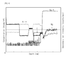
- FIG. 4 is a view showing SIMS analysis data of the light emitting device according to the embodiment.
- SIMS secondary ion mass spectrometry
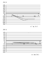
- FIGS. 5 and 6 are graphs showing reliability measurement data of the light emitting device according to the comparative example and the embodiment.
- FIG. 5 is a graph showing light output power (Po) variation data of the light emitting device according to the comparative example
- FIG. 6 is a graph showing Po variation data of the light emitting device according to the embodiment.
- FIGS. 5 and 6 are graphs showing reliability test results for two samples subject to a reliability test according to the comparative example and the embodiment.
- an AlGaInP Red LED employs a GaP window layer, and Mg is heavily doped into the GaP window layer.
- Mg existing in the GaP window layer is diffused into the active region, so that Po drop may occur.
- Mg when Mg is doped into the GaP layer, Mg is doped into the entire portion of the GaP layer at a predetermined level.
- the doping profile causes Mg diffusion into the active layer as current is applied in the LED operating/life time test (see part R).
- the Mg diffusion occurs, so that Mg profile may be adjacent to an active region on the SIMS.
- the light output power (Po) may be out of the range of ⁇ 10% when comparing with that of the initial stage of the reliability test.
- the second conductive GaP layer 162 having the first concentration and the second conductive GaP layer 164 having the second concentration higher than the first concentration may be provided on the second conductive clad layer 150.
- the second conductive GaP layer 162 having the first concentration, which is lower concentration, is grown before the second conductive GaP layer 164 having the second concentration to trap diffused Mg.
- Mg is trapped in the second conductive GaP layer 162 having the first concentration as shown in a part E of FIG. 4 to prevent Mg diffusion, so that an Mg free region is formed.
- the Po may be in the range of ⁇ 10% when comparing with that of the initial stage (0 hr) of the reliability test, which represents a stable result.
- the concentration of the second conductive GaP layer 162 may be about 10% to about 30% based on the concentration of the second conductive GaP layer 164.
- the second conductive GaP layer 164 having the second concentration may have Mg doping concentration of about 1 ⁇ 10 17 atoms/cm3 to 9 ⁇ 10 17 atoms/cm3, and the concentration of the second conductive GaP layer 162 may be about 10% to about 30% based on the Mg doping concentration of the second conductive GaP layer 164, but the embodiment is not limited thereto.
- the function of Mg trap may be difficult. If the first concentration is less than 10% based on the second concentration, the hole injection may be failed.
- FIGS. 4 and 6 show results when the first concentration is in the range of 10% to 30% based on the second concentration.
- a light emitting device which can prevent the Po drop when the reliability evaluation of the AlGaInP-based LED is performed, can be provided.
- the thickness of the second conductive GaP layer 162 having the first concentration may be about 1% to about 10% based on the thickness of the second conductive GaP layer 164 having the second concentration.
- the thickness of the second conductive GaP layer 164 having the second concentration may be in the range of about 3 ⁇ m to 4.5 ⁇ m, and the thickness of the second conductive semiconductor layer 162 having the first concentration may be in the range of about 1% to 10% based on the thickness of the second conductive GaP layer 164.
- the second conductive semiconductor layer 162 having the first concentration may serve as a hole injection barrier. If the thickness of the second conductive semiconductor layer 162 having the first concentration is less than 1% based on the thickness of the second conductive semiconductor layer 164 having the second concentration, a function of preventing the Mg diffusion may be difficult.
- the second conductive GaP layer 162 having the first concentration and the second conductive GaP layer 164 having the second concentration higher than the first concentration are provided on the second conductive clad layer 150, so that the second conductive GaP layer 162 having the first concentration prevents Mg diffusion. Accordingly, a light emitting device capable of preventing the Po drop when the reliability evaluation of the AlGaInP-based LED is performed, a method of fabricating the light emitting device, a light emitting device package, and a lighting system can be provided.
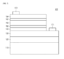
- FIG. 7 is a sectional view showing a light emitting device 102 according to a second embodiment
- FIG. 8 is a view showing a bandgap energy diagram of the light emitting device according to the second embodiment.
- the second embodiment may employ the technical feature of the first embodiment.
- an undoped AlInP-based layer 152 may be further interposed between the AlGaInP-based active layer 140 and the second conductive clad layer 150.
- a light emitting device capable of effectively preventing the Po drop by additionally preventing Mg diffusion by the undoped AlInP-based layer 152, the method of fabricating the light emitting device, a light emitting device package, and a lighting system can be provided.
- the undoped AlInP-based layer 152 may have an energy level the substantially same as that of the second conductive clad layer 150.
- the energy level of the undoped AlInP-based layer 152 is higher than the energy level of the active layer 140 to perform an electron blocking function, so that the light emission efficiency can be improved.
- the undoped AlInP-based layer 152 may have a thickness thinner than that of the second conductive clad layer 150.
- the thickness of the undoped AlInP-based layer 152 may be thinner than that of the second conductive GaP layer 162 having the first concentration.
- the substrate 110 may be a conductive substrate, but the embodiment is not limited thereto.
- the substrate 110 may include an insulating substrate.
- the substrate 110 may include a GaAs substrate, but the embodiment is not limited thereto.
- a reflective layer 120 is formed on the substrate 110 to increase the light extraction efficiency.
- the GaAs substrate absorbs the light emitted from the active layer to lower the light efficiency. Accordingly, the reflective layer 120 is formed on the substrate 110, so that the light extraction efficiency can be increased.
- the reflective layer 120 may have a distributed bragg-reflector (DBR) mirror structure in which an AlAs/AlGaAs layer and an AlGaInP/AlInP layer are sequentially deposited at a thickness of 1 ⁇ 4 wavelength (quarter-wavelength), but the embodiment is not limited thereto.
- DBR distributed bragg-reflector
- the first conductive semiconductor layer 130, the AlGaInP-based active layer 140, the undoped AlInP-based layer 152, the second conductive clad layer 150, the second conductive GaP layer 162 having the first concentration, and the second conductive GaP layer 164 having the second concentration may be sequentially formed on the reflective layer 120.
- the first conductive semiconductor layer 130 which serves as an N type contact layer, may include an N type AlGaInP-based layer or an N type AlInP layer, but the embodiment is not limited thereto.
- the AlGaInP-based active layer 140 represents higher light emission efficiency among red LED materials.
- the AlGaInP-based active layer 140 may be grown on a GaAs substrate with a compositional condition having lattice constant matching, and may be grown in the range of energy bandgap for direct transition.
- the AlGaInP-based active layer 140 may be grown through a low-pressure metal-organic chemical vapor deposition (MOCVD).
- MOCVD metal-organic chemical vapor deposition
- the undoped AlInP-based layer 152 may be additionally interposed between the AlGaInP-based active layer 140 and the second conductive clad layer 150 to be formed in the subsequent process.
- the light emitting device capable of effectively preventing the Po drop by preventing Mg diffusion by the undoped AlInP-based layer 152 can be provided.
- the undoped AlInP-based layer 152 may have the energy level the substantially same as that of the second conductive clad layer 150.
- the energy level of the undoped AlInP-based layer 152 is higher than the energy level of the active layer 140 so that the undoped AlInP-based layer 152 can serve as an electron blocking function, thereby improving the light emission efficiency.
- the undoped AlInP-based layer 152 may have a thickness thinner than that of the second conductive clad layer 150.
- the thickness of the undoped AlInP-based layer 152 may be thinner than that of the second conductive GaP layer 162 having the first concentration.
- the second conductive clad layer 150, the second conductive GaP layer 162 having the first concentration, and the second conductive GaP layer 164 having the second concentration may be formed on the undoped AlInP-based layer 152.
- the reflective layer 120, the first conductive semiconductor layer 130, the AlGaInP-based active layer 140, the undoped AlInP-based layer 152, the second conductive clad layer 150, and the second conductive GaP layer 162 having the first concentration, and the second conductive GaP layer 164 having the second concentration may include the same material composition or similar material compositions.
- the distributed bragg-reflectors rather than a metallic reflective layer are grown to have a lattice structure layer the same as that of the light emitting diode, so that a crystal can be easily grown, and the light emitting diodes have the same material composition or similar material compositions.
- the second conductive GaP layer 162 having the first concentration, which is low concentration, is grown before the second conductive GaP layer 164 having the second concentration to trap diffused Mg.
- Mg is trapped in the second conductive GaP layer 162 having the first concentration as shown in a part E of FIG. 4 to prevent Mg diffusion, so that an Mg free region is formed.
- the first concentration of the second conductive GaP layer 162 may be in the range of about 10% to about 30% based on the second concentration of the second conductive GaP layer 164.
- the second conductive GaP layer 164 having the second concentration may have Mg doping concentration of about 1 ⁇ 10 17 atoms/cm 3 to 9 ⁇ 10 17 atoms/cm 3 , and the concentration of the second conductive GaP layer 162 may be about 10% to about 30% based on the Mg doping concentration of the second conductive GaP layer 164, but the embodiment is not limited thereto.
- the function of Mg trap may not be difficult. If the first concentration is less than 10% based on the second concentration, the hole injection may be failed.
- the thickness of the second conductive GaP layer 162 having the first concentration may be in the range of about 1% to about 10% based on the thickness of the second conductive GaP layer 164 having the second concentration.
- the thickness of the second conductive GaP layer 164 having the second concentration may be in the range of about 3 ⁇ m to 4.5 ⁇ m, and may be in the range of about 1% to 10% based on the thickness of the second conductive semiconductor layer 162 having the first concentration.
- the second conductive semiconductor layer 162 having the first concentration may serve as a hole injection barrier. If the thickness of the second conductive semiconductor layer 162 having the first concentration is less than 1% based on the thickness of the second conductive semiconductor layer 164 having the second concentration, a function of preventing the Mg diffusion may be difficult.
- the second conductive GaP layer 162 having the first concentration and the second conductive GaP layer 164 having the second concentration higher than the first concentration are provided on the second conductive clad layer 150, so that the second conductive GaP layer 162 having the first concentration prevents Mg diffusion. Accordingly, a light emitting device capable of preventing the Po drop when the reliability evaluation of the AlGaInP-based LED is performed, a method of fabricating the light emitting device, a light emitting device package, and a lighting system can be provided.
- the second conductive GaP layer 164 having the second concentration, the second conductive GaP layer 162 having the first concentration, the undoped AlInP-based layer 152, the second conductive clad layer 150, the AlGaInP-based active layer 140, and the first conductive semiconductor layer 130, which are provided on the substrate 110, are sequentially etched to form a mesa structure, and first and second electrodes 171 and 172 may be formed on the second conductive semiconductor layer 130 and the second conductive GaP layer 164 having the second concentration, which are exposed to the outside, respectively.
- the substrate 110 may include a conductive substrate such as a GaAs substrate, but the embodiment is not limited thereto.
- the first electrode 171 may be formed under the substrate 110, and the second electrode 172 may be formed on the second conductive GaP layer 164 having the second concentration.
- the embodiment can provide the light emitting device capable of improving the reliability thereof by preventing the Po of the AlGaInP-based LED from being reduced, the method of fabricating the light emitting device, the light emitting device package, and the lighting system.
- FIG. 11 is a sectional view illustrating a light emitting device package 200 according to the embodiment.
- the light emitting device package 200 includes a package body 205, third and fourth electrode layers 213 and 214 formed on the package body 205, the light emitting device 100 provided on the package body 205 and electrically connected to the third and fourth electrode layers 213 and 214, and a molding member 240 that surrounds the light emitting device 100.
- the package body 205 may include silicon, synthetic resin or metallic material.
- An inclined surface may be formed around the light emitting device 100.
- the third and fourth electrode layers 213 and 214 may be electrically isolated from each other to supply power to the light emitting device 100.
- the third and fourth electrode layers 213 and 214 reflect the light emitted from the light emitting device 100 to improve the light efficiency and dissipate heat generated from the light emitting device 100 to the outside.
- the lateral type light emitting device shown in FIG. 1 can be employed as the light emitting device 100, but the embodiment is not limited thereto.
- the light emitting device 100 may be installed on the package body 205 or the third and fourth electrode layers 213 and 214.
- the light emitting device 100 is electrically connected to the third electrode layer 213 and/or the fourth electrode layer 214 through at least one of a wire bonding scheme, a flip chip bonding scheme and a die bonding scheme. According to the embodiment, the light emitting device 100 is electrically connected to the third electrode layer 213 through a wire and electrically connected to the fourth electrode layer 214 through the die bonding scheme, but the embodiment is not limited thereto.
- the molding member 230 surrounds the light emitting device 100 to protect the light emitting device 100.
- the molding member 230 may include phosphors to change the wavelength of the light emitted from the light emitting device 100.
- a plurality of light emitting device packages according to the embodiment may be arrayed on a substrate, and an optical member including a light guide plate, a prism sheet, a diffusion sheet or a fluorescent sheet may be provided on the optical path of the light emitted from the light emitting device package.
- the light emitting device package, the substrate, and the optical member may serve as a backlight unit or a lighting unit.
- the lighting system may include a backlight unit, a lighting unit, an indicator, a lamp or a streetlamp.
- FIG. 12 is an exploded perspective view an example of a lighting system including the light emitting device according to the embodiment.
- the lighting system according to the embodiment may include a cover 2100, a light source module 2200, a radiator 2400, a power supply part 2600, an inner case 2700, and a socket 2800.
- the lighting system according to the embodiment may further include at least one of a member 2300 and a holder 2500.
- the light source module 2200 may include the light emitting device 100 or the light emitting device module 200 according to the embodiment.
- the cover 2100 may have a blub shape, a hemisphere shape, a partially-open hollow shape.
- the cover 2100 may be optically coupled with the light source module 2200.
- the cover 2100 may diffuse, scatter, or excite light provided from the light source module.
- the cover 2100 may be a type of optical member.
- the cover 2100 may be coupled with the radiator 2400.
- the cover 2100 may include a coupling part which is coupled with the radiator 2400.
- the cover 2100 may include an inner surface coated with a milk-white paint.
- the milk-white paint may include a diffusion material to diffuse light.
- the cover 2100 may have the inner surface of which surface roughness is greater than that of the outer surface thereof. The surface roughness is provided for the purpose of sufficiently scattering and diffusing the light from the light source module 2200.
- a material of the cover 2100 may include glass, plastic, polypropylene (PP), polyethylene (PE), and polycarbonate (PC).
- the polycarbonate (PC) has the superior light resistance, heat resistance and strength among the above materials.
- the cover 2100 may be transparent so that a user may view the light source module 2200 from the outside, or opaque.
- the cover 2100 may be formed through a blow molding scheme.
- the light source module 220 may be disposed at one surface of the radiator 2400. Accordingly, the heat from the light source module 220 is transferred to the radiator 2400.
- the light source module 2200 may include a light source 2210, a connection plate 2230, and a connector 2250.
- the member 2300 is disposed at a top surface of the radiator 2400, and includes guide grooves 2310 into which a plurality of light sources 2210 and the connector 2250 are inserted.
- the guide grooves 2310 correspond to a substrate of the light source 2210 and the connector 2250.
- a surface of the member 2300 may be coated with a light reflective material.
- the surface of the member 2300 may be coated with white paint.
- the member 2300 again reflects light, which is reflected by the inner surface of the cover 2100 and is returned to the direction of the light source module 2200, to the direction of the cover 2100. Accordingly, the light efficiency of the lighting system according to the embodiment may be improved.
- the member 2300 may include an insulating material.
- the connection plate 2230 of the light source module 2200 may include an electrically conductive material.
- the radiator 2400 may be electrically connected to the connection plate 2230.
- the member 2300 may be configured by an insulating material, thereby preventing the connection plate 2230 from being electrically shorted with the radiator 2400.
- the radiator 2400 receives heat from the light source module 2200 and the power supply part 2600 and radiates the heat.
- the holder 2500 covers a receiving groove 2719 of an insulating part 2710 of an inner case 2700. Accordingly, the power supply part 2600 received in the insulating part 2710 of the inner case 2700 is closed.
- the holder 2500 includes a guide protrusion 2510.
- the guide protrusion 2510 has a hole through a protrusion of the power supply part 2600.
- the power supply part 2600 processes or converts an electric signal received from the outside and provides the processed or converted electric signal to the light source module 2200.
- the power supply part 2600 is received in the receiving groove of the inner case 2700, and is closed inside the inner case 2700 by the holder 2500.
- the power supply part 2600 may include a protrusion 2610, a guide part 2630, a base 2650, and an extension part 2670.
- the guide part 2630 has a shape protruding from one side of the base 2650 to the outside.
- the guide part 2630 may be inserted into the holder 2500.
- a plurality of components may be disposed above one surface of the base 2650.
- the components may include a DC converter converting AC power provided from an external power supply into DC power, a driving chip controlling driving of the light source module 2200, and an electrostatic discharge (ESD) protection device protecting the light source module 2200, but the embodiment is not limited thereto.
- the extension part 2670 has a shape protruding from an opposite side of the base 2650 to the outside.
- the extension part 2670 is inserted into an inside of the connection part 2750 of the inner case 2700, and receives an electric signal from the outside.
- a width of the extension part 2670 may be smaller than or equal to a width of the connection part 2750 of the inner case 2700.
- First terminals of a "+ electric wire” and a "- electric wire” are electrically connected to the extension part 2670 and second terminals of the "+ electric wire” and the "-electric wire” may be electrically connected to a socket 2800.
- the inner case 2700 may include a molding part therein together with the power supply part 2600.
- the molding part is prepared by hardening molding liquid, and the power supply part 2600 may be fixed inside the inner case 2700 by the molding part.
- the light extraction efficiency can be increased.
- the optical efficiency can be increased.
- any reference in this specification to "one embodiment,” “an embodiment,” “example embodiment,” etc. means that a particular feature, structure, or characteristic described in connection with the embodiment is included in at least one embodiment of the invention.
- the appearances of such phrases in various places in the specification are not necessarily all referring to the same embodiment.
Landscapes
- Led Devices (AREA)
- Non-Portable Lighting Devices Or Systems Thereof (AREA)
Abstract
Description
- The embodiment relates to a light emitting device, a method of fabricating the light emitting device, a light emitting device package, and a lighting system.
- A light emitting device includes a P-N junction diode having a characteristic of converting electrical energy into light energy. The light emitting device may include compound semiconductors belonging to group III and V on the periodic table. The light emitting device can represent various colors by adjusting the compositional ratio of the compound semiconductors.
- When forward voltage is applied to the LED, electrons of an N layer are combined with holes of a P layer, so that energy corresponding to an energy gap between a conduction band and a valance band may be generated. The energy is mainly emitted in the form of heat or light. In the case of the LED, the energy is generated in the form of light.
- For example, a nitride semiconductor represents superior thermal stability and wide bandgap energy so that the nitride semiconductor has been spotlighted in the field of optical devices and high-power electronic devices. In particular, blue, green, and UV light emitting devices employing the nitride semiconductor have already been commercialized and extensively used.
- Among light emitting diodes having a visible ray region, a light emitting diode (red LED) having a wavelength representing high utilization is a red element, which represents a superior visibility in the same brightness as compared with green and yellow elements. Accordingly, the red element has been extensively used for various fields such as traffic lights, stop lamps of vehicles, and various displays.
- Meanwhile, in the case of a red LED according to the related art, since low power is required, low current is applied, so that magnesium (Mg) diffusion issues may not be important. However, recently, as the demand for a high-power red LED chip is increased, high current is applied, so that the Mg diffusion issue into the active region has been spotlighted, and Mg existing in a GaP window layer is diffused in an active region when a reliability test is performed, so that light output power drip (Po drop) may occur.
- The embodiment provides a light emitting device capable of improving the reliability thereof by preventing Po of an AlGaInP-based LED from being reduced, a method of fabricating the light emitting device, a light emitting device package, and a lighting system.
- According to the embodiment, there is provided a light emitting device including a first conductive semiconductor layer, an AlGaInP-based active layer on the first conductive semiconductor layer, a second conductive clad layer on the AlGaInP-based active layer, a second conductive GaP layer having first concentration on the second conductive clad layer, and a second conductive GaP layer having second concentration higher than the first concentration on the second conductive GaP layer having the first concentration.
- In addition, the light emitting system according to the embodiment may include a light emitting unit having the light emitting device.
- As described above, the embodiment can provide the light emitting device capable of improving the reliability thereof by preventing the Po of the AlGaInP-based LED from being reduced, the method of fabricating the light emitting device, the light emitting device package, and the lighting system.
-
-
FIG. 1 is a sectional view showing a light emitting device according to a first embodiment. -
FIG. 2 is a bandgap energy diagram of the light emitting device according to the first embodiment. -
FIG. 3 is a graph showing SIMS analysis data of a light emitting device according to the comparative example. -
FIG. 4 is a graph showing SIMS analysis data of a light emitting device according to the embodiment. -
FIGS. 5 and 6 are graphs showing reliability measurement data of the light emitting device according to the comparative example and the embodiment. -
FIG. 7 is a sectional view showing a light emitting device according to a second embodiment. -
FIG. 8 is a bandgap energy diagram of the light emitting device according to the second embodiment. -
FIGS. 9 to 10 are sectional views showing a method of fabricating the light emitting device according to the embodiment. -
FIG. 11 is a sectional view illustrating a light emitting device package according to the embodiment. -
FIG. 12 is an exploded perspective view an example of a lighting system including the light emitting device according to the embodiment. - Hereinafter, a light emitting device, a light emitting device package, and a lighting system according to the embodiment will be described with reference to accompanying drawings.
- In the description of embodiments, it will be understood that when a layer (or film) is referred to as being 'on' another layer or substrate, it can be directly on another layer or substrate, or intervening layers may also be present. Further, it will be understood that when a layer is referred to as being 'under' another layer, it can be directly under another layer, and one or more intervening layers may also be present. In addition, it will also be understood that when a layer is referred to as being 'between' two layers, it can be the only layer between the two layers, or one or more intervening layers may also be present.
-
FIG. 1 is a sectional view showing alight emitting device 100 according to a first embodiment, andFIG. 2 is a bandgap energy diagram of the light emitting device according to the first embodiment. - The
light emitting device 100 according to the embodiment may include a firstconductive semiconductor layer 130, an AlGaInP-basedactive layer 140 on the firstconductive semiconductor layer 130, a secondconductive clad layer 150 on the AlGaInP-basedactive layer 140, a secondconductive GaP layer 162 having first concentration on the secondconductive clad layer 150, and a secondconductive GaP layer 164 having second concentration on the secondconductive GaP layer 162. -
FIG. 3 is a graph showing secondary ion mass spectrometry (SIMS) analysis data of a light emitting device according to a comparative example, andFIG. 4 is a view showing SIMS analysis data of the light emitting device according to the embodiment. -
FIGS. 5 and 6 are graphs showing reliability measurement data of the light emitting device according to the comparative example and the embodiment. - In detail,
FIG. 5 is a graph showing light output power (Po) variation data of the light emitting device according to the comparative example, andFIG. 6 is a graph showing Po variation data of the light emitting device according to the embodiment. -
FIGS. 5 and 6 are graphs showing reliability test results for two samples subject to a reliability test according to the comparative example and the embodiment. - As described above, since a red LED according to the related art requires low power, low current is applied, so that the Mg diffusion issue is not important. However, recently, as the demand for a high-power red LED chip is increased, high current is applied, so that the Mg diffusion issue into the active region has been spotlighted.
- For example, generally, an AlGaInP Red LED employs a GaP window layer, and Mg is heavily doped into the GaP window layer.
- Therefore, when the reliability test is performed, Mg existing in the GaP window layer is diffused into the active region, so that Po drop may occur.
- In detail, according to the related art, when Mg is doped into the GaP layer, Mg is doped into the entire portion of the GaP layer at a predetermined level. The doping profile causes Mg diffusion into the active layer as current is applied in the LED operating/life time test (see part R).
- For example, as shown in
FIG. 3 , the Mg diffusion (part R) occurs, so that Mg profile may be adjacent to an active region on the SIMS. - Therefore, as shown in
FIG. 5 , when the reliability test is performed, as the operating/life time test is performed, Mg is infiltrated into the active region, so that the light output power (Po) is dropped, thereby causing the reliability problem. - In other words, in terms of the light output power (Po), as 65 hours or 165 hours are elapsed, the light output power (Po) may be out of the range of ±10% when comparing with that of the initial stage of the reliability test.
- Meanwhile, in order to compensate for the above light output power, the second
conductive GaP layer 162 having the first concentration and the secondconductive GaP layer 164 having the second concentration higher than the first concentration may be provided on the secondconductive clad layer 150. - In other words, according to the embodiment, the second
conductive GaP layer 162 having the first concentration, which is lower concentration, is grown before the secondconductive GaP layer 164 having the second concentration to trap diffused Mg. - In detail, according to the embodiment, Mg is trapped in the second
conductive GaP layer 162 having the first concentration as shown in a part E ofFIG. 4 to prevent Mg diffusion, so that an Mg free region is formed. - In addition, therefore, as shown in
FIG. 6 , when the reliability test is performed, that is, when the LED operation/life time test is performed, the stable Po characteristic is ensured, so that the high reliability can be obtained. - In other words, in terms of the Po, as 65 hours or 165 hours are elapsed, the Po may be in the range of ±10% when comparing with that of the initial stage (0 hr) of the reliability test, which represents a stable result.
- According to the embodiment, the concentration of the second
conductive GaP layer 162 may be about 10% to about 30% based on the concentration of the secondconductive GaP layer 164. - For example, the second
conductive GaP layer 164 having the second concentration may have Mg doping concentration of about 1×10¹⁷ atoms/cm3 to 9×10¹⁷ atoms/cm3, and the concentration of the secondconductive GaP layer 162 may be about 10% to about 30% based on the Mg doping concentration of the secondconductive GaP layer 164, but the embodiment is not limited thereto. - If the first concentration exceeds 30% based on the second concentration, the function of Mg trap may be difficult. If the first concentration is less than 10% based on the second concentration, the hole injection may be failed.
-
FIGS. 4 and6 show results when the first concentration is in the range of 10% to 30% based on the second concentration. When the first concentration is in the range of 10% to 30% based on the second concentration, a light emitting device, which can prevent the Po drop when the reliability evaluation of the AlGaInP-based LED is performed, can be provided. - In addition, according to the embodiment, the thickness of the second
conductive GaP layer 162 having the first concentration may be about 1% to about 10% based on the thickness of the secondconductive GaP layer 164 having the second concentration. - For example, the thickness of the second
conductive GaP layer 164 having the second concentration may be in the range of about 3 µm to 4.5µm, and the thickness of the secondconductive semiconductor layer 162 having the first concentration may be in the range of about 1% to 10% based on the thickness of the secondconductive GaP layer 164. - If the thickness of the second
conductive semiconductor layer 162 having the first concentration exceeds 10% based on the thickness of the secondconductive semiconductor layer 164 having the second concentration, the secondconductive semiconductor layer 162 having the first concentration may serve as a hole injection barrier. If the thickness of the secondconductive semiconductor layer 162 having the first concentration is less than 1% based on the thickness of the secondconductive semiconductor layer 164 having the second concentration, a function of preventing the Mg diffusion may be difficult. - According to the embodiment, the second
conductive GaP layer 162 having the first concentration and the secondconductive GaP layer 164 having the second concentration higher than the first concentration are provided on the second conductive cladlayer 150, so that the secondconductive GaP layer 162 having the first concentration prevents Mg diffusion. Accordingly, a light emitting device capable of preventing the Po drop when the reliability evaluation of the AlGaInP-based LED is performed, a method of fabricating the light emitting device, a light emitting device package, and a lighting system can be provided. -
FIG. 7 is a sectional view showing alight emitting device 102 according to a second embodiment, andFIG. 8 is a view showing a bandgap energy diagram of the light emitting device according to the second embodiment. - The second embodiment may employ the technical feature of the first embodiment.
- According to the second embodiment, an undoped AlInP-based
layer 152 may be further interposed between the AlGaInP-basedactive layer 140 and the second conductive cladlayer 150. - Therefore, a light emitting device capable of effectively preventing the Po drop by additionally preventing Mg diffusion by the undoped AlInP-based
layer 152, the method of fabricating the light emitting device, a light emitting device package, and a lighting system can be provided. - According to the embodiment, the undoped AlInP-based
layer 152 may have an energy level the substantially same as that of the second conductive cladlayer 150. - Accordingly, the energy level of the undoped AlInP-based
layer 152 is higher than the energy level of theactive layer 140 to perform an electron blocking function, so that the light emission efficiency can be improved. - In addition, according to the embodiment, the undoped AlInP-based
layer 152 may have a thickness thinner than that of the second conductive cladlayer 150. - In addition, the thickness of the undoped AlInP-based
layer 152 may be thinner than that of the secondconductive GaP layer 162 having the first concentration. - Hereinafter, the method of fabricating the light emitting device according to the embodiment will be described with reference to
FIGS. 9 to 10 . - First, as shown in
FIG. 9 , asubstrate 110 is prepared. Thesubstrate 110 may be a conductive substrate, but the embodiment is not limited thereto. In other words, thesubstrate 110 may include an insulating substrate. For example, thesubstrate 110 may include a GaAs substrate, but the embodiment is not limited thereto. - Therefore, according to the embodiment, a
reflective layer 120 is formed on thesubstrate 110 to increase the light extraction efficiency. - In general, since a GaAs substrate is opaque, the GaAs substrate absorbs the light emitted from the active layer to lower the light efficiency. Accordingly, the
reflective layer 120 is formed on thesubstrate 110, so that the light extraction efficiency can be increased. - For example, the
reflective layer 120 may have a distributed bragg-reflector (DBR) mirror structure in which an AlAs/AlGaAs layer and an AlGaInP/AlInP layer are sequentially deposited at a thickness of ¼ wavelength (quarter-wavelength), but the embodiment is not limited thereto. - Next, the first
conductive semiconductor layer 130, the AlGaInP-basedactive layer 140, the undoped AlInP-basedlayer 152, the second conductive cladlayer 150, the secondconductive GaP layer 162 having the first concentration, and the secondconductive GaP layer 164 having the second concentration may be sequentially formed on thereflective layer 120. - The first
conductive semiconductor layer 130, which serves as an N type contact layer, may include an N type AlGaInP-based layer or an N type AlInP layer, but the embodiment is not limited thereto. - The AlGaInP-based
active layer 140 represents higher light emission efficiency among red LED materials. The AlGaInP-basedactive layer 140 may be grown on a GaAs substrate with a compositional condition having lattice constant matching, and may be grown in the range of energy bandgap for direct transition. - The AlGaInP-based
active layer 140 may be grown through a low-pressure metal-organic chemical vapor deposition (MOCVD). - According to the embodiment, the undoped AlInP-based
layer 152 may be additionally interposed between the AlGaInP-basedactive layer 140 and the second conductive cladlayer 150 to be formed in the subsequent process. - Accordingly, the light emitting device capable of effectively preventing the Po drop by preventing Mg diffusion by the undoped AlInP-based
layer 152 can be provided. - According to the embodiment, the undoped AlInP-based
layer 152 may have the energy level the substantially same as that of the second conductive cladlayer 150. - Accordingly, the energy level of the undoped AlInP-based
layer 152 is higher than the energy level of theactive layer 140 so that the undoped AlInP-basedlayer 152 can serve as an electron blocking function, thereby improving the light emission efficiency. - In addition, according to the embodiment, the undoped AlInP-based
layer 152 may have a thickness thinner than that of the second conductive cladlayer 150. - In addition, the thickness of the undoped AlInP-based
layer 152 may be thinner than that of the secondconductive GaP layer 162 having the first concentration. - Next, according to the embodiment, the second conductive clad
layer 150, the secondconductive GaP layer 162 having the first concentration, and the secondconductive GaP layer 164 having the second concentration may be formed on the undoped AlInP-basedlayer 152. - According to the embodiment, the
reflective layer 120, the firstconductive semiconductor layer 130, the AlGaInP-basedactive layer 140, the undoped AlInP-basedlayer 152, the second conductive cladlayer 150, and the secondconductive GaP layer 162 having the first concentration, and the secondconductive GaP layer 164 having the second concentration may include the same material composition or similar material compositions. - When the
reflective layer 120 is formed by taking into consideration the fabricating processes of the light emitting diodes through a growing scheme, the distributed bragg-reflectors rather than a metallic reflective layer are grown to have a lattice structure layer the same as that of the light emitting diode, so that a crystal can be easily grown, and the light emitting diodes have the same material composition or similar material compositions. - In other words, according to the embodiment, the second
conductive GaP layer 162 having the first concentration, which is low concentration, is grown before the secondconductive GaP layer 164 having the second concentration to trap diffused Mg. - In detail, according to the embodiment, Mg is trapped in the second
conductive GaP layer 162 having the first concentration as shown in a part E ofFIG. 4 to prevent Mg diffusion, so that an Mg free region is formed. - In addition, therefore, according to the embodiment, when the LED operation/life time test is performed, the stable Po characteristic is ensured.
- According to the embodiment, the first concentration of the second
conductive GaP layer 162 may be in the range of about 10% to about 30% based on the second concentration of the secondconductive GaP layer 164. - For example, the second
conductive GaP layer 164 having the second concentration may have Mg doping concentration of about 1×10¹⁷ atoms/cm3 to 9×10¹⁷ atoms/cm3, and the concentration of the secondconductive GaP layer 162 may be about 10% to about 30% based on the Mg doping concentration of the secondconductive GaP layer 164, but the embodiment is not limited thereto. - If the first concentration exceeds 30% based on the second concentration, the function of Mg trap may not be difficult. If the first concentration is less than 10% based on the second concentration, the hole injection may be failed.
- In addition, according to the embodiment, the thickness of the second
conductive GaP layer 162 having the first concentration may be in the range of about 1% to about 10% based on the thickness of the secondconductive GaP layer 164 having the second concentration. - For example, the thickness of the second
conductive GaP layer 164 having the second concentration may be in the range of about 3 µm to 4.5µm, and may be in the range of about 1% to 10% based on the thickness of the secondconductive semiconductor layer 162 having the first concentration. - If the thickness of the second
conductive semiconductor layer 162 having the first concentration exceeds 10% based on the thickness of the secondconductive semiconductor layer 164 having the second concentration, the secondconductive semiconductor layer 162 having the first concentration may serve as a hole injection barrier. If the thickness of the secondconductive semiconductor layer 162 having the first concentration is less than 1% based on the thickness of the secondconductive semiconductor layer 164 having the second concentration, a function of preventing the Mg diffusion may be difficult. - According to the embodiment, the second
conductive GaP layer 162 having the first concentration and the secondconductive GaP layer 164 having the second concentration higher than the first concentration are provided on the second conductive cladlayer 150, so that the secondconductive GaP layer 162 having the first concentration prevents Mg diffusion. Accordingly, a light emitting device capable of preventing the Po drop when the reliability evaluation of the AlGaInP-based LED is performed, a method of fabricating the light emitting device, a light emitting device package, and a lighting system can be provided. - Thereafter, when a light emitting device chip is formed in a lateral-type structure, the second
conductive GaP layer 164 having the second concentration, the secondconductive GaP layer 162 having the first concentration, the undoped AlInP-basedlayer 152, the second conductive cladlayer 150, the AlGaInP-basedactive layer 140, and the firstconductive semiconductor layer 130, which are provided on thesubstrate 110, are sequentially etched to form a mesa structure, and first andsecond electrodes conductive semiconductor layer 130 and the secondconductive GaP layer 164 having the second concentration, which are exposed to the outside, respectively. In addition, a portion of thereflective layer 120 may be removed to expose thesubstrate 110, so that thefirst electrode 171 may be formed on thesubstrate 110. In this case, thesubstrate 110 may include a conductive substrate such as a GaAs substrate, but the embodiment is not limited thereto. - Meanwhile, differently from the structure shown in
FIG. 10 , when the light emitting device is formed in a vertical-type chip structure, thefirst electrode 171 may be formed under thesubstrate 110, and thesecond electrode 172 may be formed on the secondconductive GaP layer 164 having the second concentration. - The embodiment can provide the light emitting device capable of improving the reliability thereof by preventing the Po of the AlGaInP-based LED from being reduced, the method of fabricating the light emitting device, the light emitting device package, and the lighting system.
-
FIG. 11 is a sectional view illustrating a light emittingdevice package 200 according to the embodiment. - The light emitting
device package 200 according to the embodiment includes apackage body 205, third and fourth electrode layers 213 and 214 formed on thepackage body 205, thelight emitting device 100 provided on thepackage body 205 and electrically connected to the third and fourth electrode layers 213 and 214, and a molding member 240 that surrounds thelight emitting device 100. - The
package body 205 may include silicon, synthetic resin or metallic material. An inclined surface may be formed around thelight emitting device 100. - The third and fourth electrode layers 213 and 214 may be electrically isolated from each other to supply power to the
light emitting device 100. In addition, the third and fourth electrode layers 213 and 214 reflect the light emitted from thelight emitting device 100 to improve the light efficiency and dissipate heat generated from thelight emitting device 100 to the outside. - The lateral type light emitting device shown in
FIG. 1 can be employed as thelight emitting device 100, but the embodiment is not limited thereto. - The
light emitting device 100 may be installed on thepackage body 205 or the third and fourth electrode layers 213 and 214. - The
light emitting device 100 is electrically connected to thethird electrode layer 213 and/or thefourth electrode layer 214 through at least one of a wire bonding scheme, a flip chip bonding scheme and a die bonding scheme. According to the embodiment, thelight emitting device 100 is electrically connected to thethird electrode layer 213 through a wire and electrically connected to thefourth electrode layer 214 through the die bonding scheme, but the embodiment is not limited thereto. - The
molding member 230 surrounds thelight emitting device 100 to protect thelight emitting device 100. In addition, themolding member 230 may include phosphors to change the wavelength of the light emitted from thelight emitting device 100. - A plurality of light emitting device packages according to the embodiment may be arrayed on a substrate, and an optical member including a light guide plate, a prism sheet, a diffusion sheet or a fluorescent sheet may be provided on the optical path of the light emitted from the light emitting device package. The light emitting device package, the substrate, and the optical member may serve as a backlight unit or a lighting unit. For instance, the lighting system may include a backlight unit, a lighting unit, an indicator, a lamp or a streetlamp.
-
FIG. 12 is an exploded perspective view an example of a lighting system including the light emitting device according to the embodiment. - As shown in
FIG. 12 , the lighting system according to the embodiment may include acover 2100, alight source module 2200, aradiator 2400, apower supply part 2600, aninner case 2700, and asocket 2800. The lighting system according to the embodiment may further include at least one of amember 2300 and aholder 2500. Thelight source module 2200 may include thelight emitting device 100 or the light emittingdevice module 200 according to the embodiment. - For example, the
cover 2100 may have a blub shape, a hemisphere shape, a partially-open hollow shape. Thecover 2100 may be optically coupled with thelight source module 2200. For example, thecover 2100 may diffuse, scatter, or excite light provided from the light source module. Thecover 2100 may be a type of optical member. Thecover 2100 may be coupled with theradiator 2400. Thecover 2100 may include a coupling part which is coupled with theradiator 2400. - The
cover 2100 may include an inner surface coated with a milk-white paint. The milk-white paint may include a diffusion material to diffuse light. Thecover 2100 may have the inner surface of which surface roughness is greater than that of the outer surface thereof. The surface roughness is provided for the purpose of sufficiently scattering and diffusing the light from thelight source module 2200. - For example, a material of the
cover 2100 may include glass, plastic, polypropylene (PP), polyethylene (PE), and polycarbonate (PC). The polycarbonate (PC) has the superior light resistance, heat resistance and strength among the above materials. Thecover 2100 may be transparent so that a user may view thelight source module 2200 from the outside, or opaque. Thecover 2100 may be formed through a blow molding scheme. - The light source module 220 may be disposed at one surface of the
radiator 2400. Accordingly, the heat from the light source module 220 is transferred to theradiator 2400. Thelight source module 2200 may include alight source 2210, aconnection plate 2230, and aconnector 2250. - The
member 2300 is disposed at a top surface of theradiator 2400, and includesguide grooves 2310 into which a plurality oflight sources 2210 and theconnector 2250 are inserted. Theguide grooves 2310 correspond to a substrate of thelight source 2210 and theconnector 2250. - A surface of the
member 2300 may be coated with a light reflective material. For example, the surface of themember 2300 may be coated with white paint. Themember 2300 again reflects light, which is reflected by the inner surface of thecover 2100 and is returned to the direction of thelight source module 2200, to the direction of thecover 2100. Accordingly, the light efficiency of the lighting system according to the embodiment may be improved. - For example, the
member 2300 may include an insulating material. Theconnection plate 2230 of thelight source module 2200 may include an electrically conductive material. Accordingly, theradiator 2400 may be electrically connected to theconnection plate 2230. Themember 2300 may be configured by an insulating material, thereby preventing theconnection plate 2230 from being electrically shorted with theradiator 2400. Theradiator 2400 receives heat from thelight source module 2200 and thepower supply part 2600 and radiates the heat. - The
holder 2500 covers a receivinggroove 2719 of aninsulating part 2710 of aninner case 2700. Accordingly, thepower supply part 2600 received in the insulatingpart 2710 of theinner case 2700 is closed. Theholder 2500 includes aguide protrusion 2510. Theguide protrusion 2510 has a hole through a protrusion of thepower supply part 2600. - The
power supply part 2600 processes or converts an electric signal received from the outside and provides the processed or converted electric signal to thelight source module 2200. Thepower supply part 2600 is received in the receiving groove of theinner case 2700, and is closed inside theinner case 2700 by theholder 2500. - The
power supply part 2600 may include aprotrusion 2610, aguide part 2630, abase 2650, and anextension part 2670. - The
guide part 2630 has a shape protruding from one side of the base 2650 to the outside. Theguide part 2630 may be inserted into theholder 2500. A plurality of components may be disposed above one surface of thebase 2650. For example, the components may include a DC converter converting AC power provided from an external power supply into DC power, a driving chip controlling driving of thelight source module 2200, and an electrostatic discharge (ESD) protection device protecting thelight source module 2200, but the embodiment is not limited thereto. - The
extension part 2670 has a shape protruding from an opposite side of the base 2650 to the outside. Theextension part 2670 is inserted into an inside of theconnection part 2750 of theinner case 2700, and receives an electric signal from the outside. For example, a width of theextension part 2670 may be smaller than or equal to a width of theconnection part 2750 of theinner case 2700. First terminals of a "+ electric wire" and a "- electric wire" are electrically connected to theextension part 2670 and second terminals of the "+ electric wire" and the "-electric wire" may be electrically connected to asocket 2800. - The
inner case 2700 may include a molding part therein together with thepower supply part 2600. The molding part is prepared by hardening molding liquid, and thepower supply part 2600 may be fixed inside theinner case 2700 by the molding part. - According to the light emitting device, the method of manufacturing the same, the light emitting package, and the lighting system of the embodiment, the light extraction efficiency can be increased.
- In addition, according to the embodiment, the optical efficiency can be increased.
- Any reference in this specification to "one embodiment," "an embodiment," "example embodiment," etc., means that a particular feature, structure, or characteristic described in connection with the embodiment is included in at least one embodiment of the invention. The appearances of such phrases in various places in the specification are not necessarily all referring to the same embodiment. Further, when a particular feature, structure, or characteristic is described in connection with any embodiment, it is submitted that it is within the purview of one skilled in the art to effect such feature, structure, or characteristic in connection with other ones of the embodiments.
- Although embodiments have been described with reference to a number of illustrative embodiments thereof, it should be understood that numerous other modifications and embodiments can be devised by those skilled in the art that will fall within the spirit and scope of the principles of this disclosure. More particularly, various variations and modifications are possible in the component parts and/or arrangements of the subject combination arrangement within the scope of the disclosure, the drawings and the appended claims. In addition to variations and modifications in the component parts and/or arrangements, alternative uses will also be apparent to those skilled in the art.
Claims (15)
- A light emitting device comprising:a first conductive semiconductor layer (130);an AlGaInP-based active layer (140) on the first conductive semiconductor layer (130);a second conductive clad layer (150) on the AlGaInP-based active layer (140);a second conductive GaP layer (162) having first concentration on the second conductive clad layer (150); anda second conductive GaP layer (164) having second concentration higher than the first concentration on the second conductive GaP layer (162) having the first concentration.
- The light emitting device of claim 1, wherein the first concentration of the second conductive GaP layer (162) is in a range of 10% to 30% based on the second concentration of the second conductive GaP layer (164).
- The light emitting device of claim 1 or claim 2, wherein the second conductive GaP layer (164) having the second concentration has Mg doping concentration in a range of 1×10¹⁷ atoms/cm3 to 9×10¹⁷ atoms/cm3.
- The light emitting device of at least one of claims 1 to 3, wherein the second conductive GaP layer (162) having the first concentration traps magnesium (Mg) therein to prevent Mg diffusion, such that an Mg free region is formed.
- The light emitting device of at least one of claims 1 to 4, wherein the second conductive GaP layer (162) having the first concentration has a thickness thinner than a thickness of the second conductive GaP layer (164) having the second concentration.
- The light emitting device of at least one of claims 1 to 5, wherein the thickness of the second conductive GaP layer (162) having the first concentration is in a range of 1% to 10% based on the thickness of the second conductive GaP layer (164) having the second concentration.
- The light emitting device of at least one of claims 1 to 6, wherein the thickness of the second conductive GaP layer (164) having the second concentration is in a range of 3 µm to 4.5 µm.
- The light emitting device of at least one of claims 1 to 7, further comprising an undoped AlInP-based layer (152) interposed between the AlGaInP-based active layer (140) and the second conductive clad layer (150).
- The light emitting device of claim 8, wherein the undoped AlInP-based layer (152) prevents Mg diffusion.
- The light emitting device of claim 8, wherein the undoped AlInP-based layer (152) has an energy level substantially equal to an energy level of the second conductive clad layer (150).
- The light emitting device of claim 8, wherein the undoped AlInP-based layer (152) is thinner than the second conductive clad layer (150).
- The light emitting device of claim 8, wherein the undoped AlInP-based layer (152) is thinner than the second conductive GaP layer(162) having the first concentration.
- The light emitting device of at least one of claims 1 to 12, further comprising a reflective layer (120) on a bottom surface of the first conductive semiconductor layer (130).
- The light emitting device of at least one of claims 1 to 13, wherein the first conductive semiconductor layer (130), the AlGaInP-based active layer (140), the second conductive clad layer (150), and the second conductive GaP layer (162) having the first concentration, and the second conductive GaP layer (164) having the second concentration comprise a same material composition or similar material compositions.
- A lighting system comprising a lighting unit including the light emitting device according to at least one of claims 1 to 14.
Applications Claiming Priority (1)
| Application Number | Priority Date | Filing Date | Title |
|---|---|---|---|
| KR1020130069663A KR102101356B1 (en) | 2013-06-18 | 2013-06-18 | Light emitting device, and lighting system |
Publications (2)
| Publication Number | Publication Date |
|---|---|
| EP2816615A1 true EP2816615A1 (en) | 2014-12-24 |
| EP2816615B1 EP2816615B1 (en) | 2019-09-11 |
Family
ID=51210224
Family Applications (1)
| Application Number | Title | Priority Date | Filing Date |
|---|---|---|---|
| EP14172841.0A Active EP2816615B1 (en) | 2013-06-18 | 2014-06-17 | Light emitting device and lighting system |
Country Status (5)
| Country | Link |
|---|---|
| US (1) | US9147811B2 (en) |
| EP (1) | EP2816615B1 (en) |
| JP (1) | JP6426377B2 (en) |
| KR (1) | KR102101356B1 (en) |
| CN (1) | CN104241474B (en) |
Families Citing this family (5)
| Publication number | Priority date | Publication date | Assignee | Title |
|---|---|---|---|---|
| US11557693B2 (en) | 2017-07-31 | 2023-01-17 | Xiamen San'an Optoelectronics Co., Ltd. | Semiconductor light emitting device |
| CN107394019B (en) * | 2017-07-31 | 2019-07-12 | 安徽三安光电有限公司 | A kind of semiconductor light-emitting element and preparation method thereof |
| US10978612B2 (en) | 2017-07-31 | 2021-04-13 | Xiamen San'an Optoelectronics Co., Ltd | Semiconductor light emitting device |
| CN110379898B (en) * | 2019-05-22 | 2020-11-17 | 华灿光电(苏州)有限公司 | Light emitting diode epitaxial wafer and growth method thereof |
| KR20240112402A (en) * | 2023-01-11 | 2024-07-19 | 삼성디스플레이 주식회사 | Display device and manufacturing method thereof |
Citations (4)
| Publication number | Priority date | Publication date | Assignee | Title |
|---|---|---|---|---|
| US20060163603A1 (en) * | 2003-02-10 | 2006-07-27 | Ryouichi Takeuchi | Light-emitting diode device and production method thereof |
| US20070023768A1 (en) * | 2005-08-01 | 2007-02-01 | Hitachi Cable, Ltd. | Semiconductor light emitting element |
| US20090140273A1 (en) * | 2007-11-30 | 2009-06-04 | Hitachi Cable, Ltd. | Epitaxial Wafer for Semiconductor Light Emitting Diode and Semiconductor Light Emitting Diode Using Same |
| US20110198634A1 (en) * | 2010-02-16 | 2011-08-18 | Stanley Electric Co., Ltd. | Semiconductor light-emitting apparatus and method of manufacturing the same |
Family Cites Families (15)
| Publication number | Priority date | Publication date | Assignee | Title |
|---|---|---|---|---|
| JP3164478B2 (en) * | 1994-08-31 | 2001-05-08 | 京セラ株式会社 | Semiconductor device and method of manufacturing the same |
| JP3122324B2 (en) * | 1995-02-20 | 2001-01-09 | 三菱電線工業株式会社 | Semiconductor light emitting device |
| JPH0945959A (en) * | 1995-07-28 | 1997-02-14 | Toshiba Corp | Light emitting element |
| JP3966962B2 (en) * | 1997-10-16 | 2007-08-29 | スタンレー電気株式会社 | Light emitting diode and manufacturing method thereof |
| JP2000174338A (en) * | 1998-12-02 | 2000-06-23 | Matsushita Electric Ind Co Ltd | Gallium nitride based compound semiconductor light emitting device |
| US6608328B2 (en) * | 2001-02-05 | 2003-08-19 | Uni Light Technology Inc. | Semiconductor light emitting diode on a misoriented substrate |
| JP4255710B2 (en) * | 2003-02-10 | 2009-04-15 | 昭和電工株式会社 | Semiconductor light emitting device |
| TWI231053B (en) * | 2003-02-10 | 2005-04-11 | Showa Denko Kk | Semiconductor light emitting device and the manufacturing method thereof |
| US8399948B2 (en) * | 2009-12-04 | 2013-03-19 | Lg Innotek Co., Ltd. | Light emitting device, light emitting device package and lighting system |
| KR101028286B1 (en) * | 2009-12-28 | 2011-04-11 | 엘지이노텍 주식회사 | Semiconductor light emitting device and manufacturing method thereof |
| KR101028251B1 (en) * | 2010-01-19 | 2011-04-11 | 엘지이노텍 주식회사 | Semiconductor light emitting device and manufacturing method thereof |
| JP2011222950A (en) * | 2010-03-24 | 2011-11-04 | Showa Denko Kk | Light emitting diode |
| JP5648475B2 (en) | 2010-12-28 | 2015-01-07 | 信越半導体株式会社 | Light emitting element |
| KR20120103817A (en) | 2011-03-11 | 2012-09-20 | 서울옵토디바이스주식회사 | Method of manufacturing light emitting diode |
| JP2013042082A (en) * | 2011-08-19 | 2013-02-28 | Hitachi Cable Ltd | Semiconductor light-emitting element |
-
2013
- 2013-06-18 KR KR1020130069663A patent/KR102101356B1/en active Active
-
2014
- 2014-06-16 JP JP2014123447A patent/JP6426377B2/en active Active
- 2014-06-17 CN CN201410270175.4A patent/CN104241474B/en active Active
- 2014-06-17 EP EP14172841.0A patent/EP2816615B1/en active Active
- 2014-06-17 US US14/307,038 patent/US9147811B2/en active Active
Patent Citations (4)
| Publication number | Priority date | Publication date | Assignee | Title |
|---|---|---|---|---|
| US20060163603A1 (en) * | 2003-02-10 | 2006-07-27 | Ryouichi Takeuchi | Light-emitting diode device and production method thereof |
| US20070023768A1 (en) * | 2005-08-01 | 2007-02-01 | Hitachi Cable, Ltd. | Semiconductor light emitting element |
| US20090140273A1 (en) * | 2007-11-30 | 2009-06-04 | Hitachi Cable, Ltd. | Epitaxial Wafer for Semiconductor Light Emitting Diode and Semiconductor Light Emitting Diode Using Same |
| US20110198634A1 (en) * | 2010-02-16 | 2011-08-18 | Stanley Electric Co., Ltd. | Semiconductor light-emitting apparatus and method of manufacturing the same |
Also Published As
| Publication number | Publication date |
|---|---|
| JP6426377B2 (en) | 2018-11-21 |
| KR102101356B1 (en) | 2020-04-17 |
| US9147811B2 (en) | 2015-09-29 |
| US20140367715A1 (en) | 2014-12-18 |
| KR20140146839A (en) | 2014-12-29 |
| CN104241474A (en) | 2014-12-24 |
| EP2816615B1 (en) | 2019-09-11 |
| CN104241474B (en) | 2017-11-14 |
| JP2015005745A (en) | 2015-01-08 |
Similar Documents
| Publication | Publication Date | Title |
|---|---|---|
| US9660160B2 (en) | Light emitting device | |
| US9496457B2 (en) | Light emitting device and light emitting device package | |
| US20110095263A1 (en) | Light emitting device and light emitting device package | |
| EP2816615B1 (en) | Light emitting device and lighting system | |
| US11227973B2 (en) | Semiconductor device | |
| KR20150012950A (en) | Light Emitting Device Package | |
| US9559257B2 (en) | Light emitting device and lighting system | |
| CN110537262A (en) | Semiconductor device | |
| KR20120079668A (en) | Led package and method thereof | |
| KR102187501B1 (en) | Light emitting device | |
| US20150123158A1 (en) | Light emitting device | |
| KR20150069824A (en) | Light emitting device | |
| US10008633B2 (en) | Light-emitting diode and lighting system | |
| KR102140277B1 (en) | Light Emitting Device | |
| US9246058B2 (en) | Light emitting device | |
| KR102187514B1 (en) | Light emitting device | |
| KR20150092478A (en) | Light Emitting Device | |
| KR20160066368A (en) | Light emitting device, light emitting device package having the same, and light system having the same | |
| KR102212730B1 (en) | Light emitting device | |
| KR102187508B1 (en) | Light emitting device | |
| KR102109039B1 (en) | Light emitting device and light emitting device package including the same | |
| US9837588B2 (en) | Light-emitting device package and lighting apparatus including the package | |
| KR102107523B1 (en) | Light Emitting Device Package | |
| KR20160019799A (en) | Light emitting device | |
| KR20200048778A (en) | Light emitting device |
Legal Events
| Date | Code | Title | Description |
|---|---|---|---|
| PUAI | Public reference made under article 153(3) epc to a published international application that has entered the european phase |
Free format text: ORIGINAL CODE: 0009012 |
|
| 17P | Request for examination filed |
Effective date: 20140710 |
|
| AK | Designated contracting states |
Kind code of ref document: A1 Designated state(s): AL AT BE BG CH CY CZ DE DK EE ES FI FR GB GR HR HU IE IS IT LI LT LU LV MC MK MT NL NO PL PT RO RS SE SI SK SM TR |
|
| AX | Request for extension of the european patent |
Extension state: BA ME |
|
| RBV | Designated contracting states (corrected) |
Designated state(s): AL AT BE BG CH CY CZ DE DK EE ES FI FR GB GR HR HU IE IS IT LI LT LU LV MC MK MT NL NO PL PT RO RS SE SI SK SM TR |
|
| 17Q | First examination report despatched |
Effective date: 20160616 |
|
| RAP1 | Party data changed (applicant data changed or rights of an application transferred) |
Owner name: LG INNOTEK CO., LTD. |
|
| STAA | Information on the status of an ep patent application or granted ep patent |
Free format text: STATUS: EXAMINATION IS IN PROGRESS |
|
| GRAP | Despatch of communication of intention to grant a patent |
Free format text: ORIGINAL CODE: EPIDOSNIGR1 |
|
| STAA | Information on the status of an ep patent application or granted ep patent |
Free format text: STATUS: GRANT OF PATENT IS INTENDED |
|
| RIC1 | Information provided on ipc code assigned before grant |
Ipc: H01L 33/30 20100101ALI20190315BHEP Ipc: H01L 33/02 20100101AFI20190315BHEP Ipc: H01L 33/10 20100101ALI20190315BHEP Ipc: H01L 33/14 20100101ALI20190315BHEP |
|
| INTG | Intention to grant announced |
Effective date: 20190417 |
|
| GRAS | Grant fee paid |
Free format text: ORIGINAL CODE: EPIDOSNIGR3 |
|
| GRAA | (expected) grant |
Free format text: ORIGINAL CODE: 0009210 |
|
| STAA | Information on the status of an ep patent application or granted ep patent |
Free format text: STATUS: THE PATENT HAS BEEN GRANTED |
|
| AK | Designated contracting states |
Kind code of ref document: B1 Designated state(s): AL AT BE BG CH CY CZ DE DK EE ES FI FR GB GR HR HU IE IS IT LI LT LU LV MC MK MT NL NO PL PT RO RS SE SI SK SM TR |
|
| REG | Reference to a national code |
Ref country code: GB Ref legal event code: FG4D |
|
| REG | Reference to a national code |
Ref country code: CH Ref legal event code: EP |
|
| REG | Reference to a national code |
Ref country code: AT Ref legal event code: REF Ref document number: 1179603 Country of ref document: AT Kind code of ref document: T Effective date: 20190915 |
|
| REG | Reference to a national code |
Ref country code: DE Ref legal event code: R096 Ref document number: 602014053311 Country of ref document: DE Ref country code: IE Ref legal event code: FG4D |
|
| REG | Reference to a national code |
Ref country code: NL Ref legal event code: FP |
|
| REG | Reference to a national code |
Ref country code: LT Ref legal event code: MG4D |
|
| PG25 | Lapsed in a contracting state [announced via postgrant information from national office to epo] |
Ref country code: LT Free format text: LAPSE BECAUSE OF FAILURE TO SUBMIT A TRANSLATION OF THE DESCRIPTION OR TO PAY THE FEE WITHIN THE PRESCRIBED TIME-LIMIT Effective date: 20190911 Ref country code: HR Free format text: LAPSE BECAUSE OF FAILURE TO SUBMIT A TRANSLATION OF THE DESCRIPTION OR TO PAY THE FEE WITHIN THE PRESCRIBED TIME-LIMIT Effective date: 20190911 Ref country code: NO Free format text: LAPSE BECAUSE OF FAILURE TO SUBMIT A TRANSLATION OF THE DESCRIPTION OR TO PAY THE FEE WITHIN THE PRESCRIBED TIME-LIMIT Effective date: 20191211 Ref country code: FI Free format text: LAPSE BECAUSE OF FAILURE TO SUBMIT A TRANSLATION OF THE DESCRIPTION OR TO PAY THE FEE WITHIN THE PRESCRIBED TIME-LIMIT Effective date: 20190911 Ref country code: SE Free format text: LAPSE BECAUSE OF FAILURE TO SUBMIT A TRANSLATION OF THE DESCRIPTION OR TO PAY THE FEE WITHIN THE PRESCRIBED TIME-LIMIT Effective date: 20190911 Ref country code: BG Free format text: LAPSE BECAUSE OF FAILURE TO SUBMIT A TRANSLATION OF THE DESCRIPTION OR TO PAY THE FEE WITHIN THE PRESCRIBED TIME-LIMIT Effective date: 20191211 |
|
| PG25 | Lapsed in a contracting state [announced via postgrant information from national office to epo] |
Ref country code: RS Free format text: LAPSE BECAUSE OF FAILURE TO SUBMIT A TRANSLATION OF THE DESCRIPTION OR TO PAY THE FEE WITHIN THE PRESCRIBED TIME-LIMIT Effective date: 20190911 Ref country code: LV Free format text: LAPSE BECAUSE OF FAILURE TO SUBMIT A TRANSLATION OF THE DESCRIPTION OR TO PAY THE FEE WITHIN THE PRESCRIBED TIME-LIMIT Effective date: 20190911 Ref country code: AL Free format text: LAPSE BECAUSE OF FAILURE TO SUBMIT A TRANSLATION OF THE DESCRIPTION OR TO PAY THE FEE WITHIN THE PRESCRIBED TIME-LIMIT Effective date: 20190911 Ref country code: ES Free format text: LAPSE BECAUSE OF FAILURE TO SUBMIT A TRANSLATION OF THE DESCRIPTION OR TO PAY THE FEE WITHIN THE PRESCRIBED TIME-LIMIT Effective date: 20190911 Ref country code: GR Free format text: LAPSE BECAUSE OF FAILURE TO SUBMIT A TRANSLATION OF THE DESCRIPTION OR TO PAY THE FEE WITHIN THE PRESCRIBED TIME-LIMIT Effective date: 20191212 |
|
| REG | Reference to a national code |
Ref country code: AT Ref legal event code: MK05 Ref document number: 1179603 Country of ref document: AT Kind code of ref document: T Effective date: 20190911 |
|
| PG25 | Lapsed in a contracting state [announced via postgrant information from national office to epo] |
Ref country code: AT Free format text: LAPSE BECAUSE OF FAILURE TO SUBMIT A TRANSLATION OF THE DESCRIPTION OR TO PAY THE FEE WITHIN THE PRESCRIBED TIME-LIMIT Effective date: 20190911 Ref country code: PT Free format text: LAPSE BECAUSE OF FAILURE TO SUBMIT A TRANSLATION OF THE DESCRIPTION OR TO PAY THE FEE WITHIN THE PRESCRIBED TIME-LIMIT Effective date: 20200113 Ref country code: PL Free format text: LAPSE BECAUSE OF FAILURE TO SUBMIT A TRANSLATION OF THE DESCRIPTION OR TO PAY THE FEE WITHIN THE PRESCRIBED TIME-LIMIT Effective date: 20190911 Ref country code: RO Free format text: LAPSE BECAUSE OF FAILURE TO SUBMIT A TRANSLATION OF THE DESCRIPTION OR TO PAY THE FEE WITHIN THE PRESCRIBED TIME-LIMIT Effective date: 20190911 Ref country code: IT Free format text: LAPSE BECAUSE OF FAILURE TO SUBMIT A TRANSLATION OF THE DESCRIPTION OR TO PAY THE FEE WITHIN THE PRESCRIBED TIME-LIMIT Effective date: 20190911 Ref country code: EE Free format text: LAPSE BECAUSE OF FAILURE TO SUBMIT A TRANSLATION OF THE DESCRIPTION OR TO PAY THE FEE WITHIN THE PRESCRIBED TIME-LIMIT Effective date: 20190911 |
|
| PG25 | Lapsed in a contracting state [announced via postgrant information from national office to epo] |
Ref country code: SM Free format text: LAPSE BECAUSE OF FAILURE TO SUBMIT A TRANSLATION OF THE DESCRIPTION OR TO PAY THE FEE WITHIN THE PRESCRIBED TIME-LIMIT Effective date: 20190911 Ref country code: CZ Free format text: LAPSE BECAUSE OF FAILURE TO SUBMIT A TRANSLATION OF THE DESCRIPTION OR TO PAY THE FEE WITHIN THE PRESCRIBED TIME-LIMIT Effective date: 20190911 Ref country code: IS Free format text: LAPSE BECAUSE OF FAILURE TO SUBMIT A TRANSLATION OF THE DESCRIPTION OR TO PAY THE FEE WITHIN THE PRESCRIBED TIME-LIMIT Effective date: 20200224 Ref country code: SK Free format text: LAPSE BECAUSE OF FAILURE TO SUBMIT A TRANSLATION OF THE DESCRIPTION OR TO PAY THE FEE WITHIN THE PRESCRIBED TIME-LIMIT Effective date: 20190911 |
|
| REG | Reference to a national code |
Ref country code: DE Ref legal event code: R097 Ref document number: 602014053311 Country of ref document: DE |
|
| PLBE | No opposition filed within time limit |
Free format text: ORIGINAL CODE: 0009261 |
|
| STAA | Information on the status of an ep patent application or granted ep patent |
Free format text: STATUS: NO OPPOSITION FILED WITHIN TIME LIMIT |
|
| PG2D | Information on lapse in contracting state deleted |
Ref country code: IS |
|
| PG25 | Lapsed in a contracting state [announced via postgrant information from national office to epo] |
Ref country code: DK Free format text: LAPSE BECAUSE OF FAILURE TO SUBMIT A TRANSLATION OF THE DESCRIPTION OR TO PAY THE FEE WITHIN THE PRESCRIBED TIME-LIMIT Effective date: 20190911 Ref country code: IS Free format text: LAPSE BECAUSE OF FAILURE TO SUBMIT A TRANSLATION OF THE DESCRIPTION OR TO PAY THE FEE WITHIN THE PRESCRIBED TIME-LIMIT Effective date: 20200112 |
|
| 26N | No opposition filed |
Effective date: 20200615 |
|
| PG25 | Lapsed in a contracting state [announced via postgrant information from national office to epo] |
Ref country code: SI Free format text: LAPSE BECAUSE OF FAILURE TO SUBMIT A TRANSLATION OF THE DESCRIPTION OR TO PAY THE FEE WITHIN THE PRESCRIBED TIME-LIMIT Effective date: 20190911 |
|
| PG25 | Lapsed in a contracting state [announced via postgrant information from national office to epo] |
Ref country code: MC Free format text: LAPSE BECAUSE OF FAILURE TO SUBMIT A TRANSLATION OF THE DESCRIPTION OR TO PAY THE FEE WITHIN THE PRESCRIBED TIME-LIMIT Effective date: 20190911 |
|
| REG | Reference to a national code |
Ref country code: CH Ref legal event code: PL |
|
| GBPC | Gb: european patent ceased through non-payment of renewal fee |
Effective date: 20200617 |
|
| PG25 | Lapsed in a contracting state [announced via postgrant information from national office to epo] |
Ref country code: LU Free format text: LAPSE BECAUSE OF NON-PAYMENT OF DUE FEES Effective date: 20200617 |
|
| REG | Reference to a national code |
Ref country code: BE Ref legal event code: MM Effective date: 20200630 |
|
| PG25 | Lapsed in a contracting state [announced via postgrant information from national office to epo] |
Ref country code: GB Free format text: LAPSE BECAUSE OF NON-PAYMENT OF DUE FEES Effective date: 20200617 Ref country code: LI Free format text: LAPSE BECAUSE OF NON-PAYMENT OF DUE FEES Effective date: 20200630 Ref country code: IE Free format text: LAPSE BECAUSE OF NON-PAYMENT OF DUE FEES Effective date: 20200617 Ref country code: CH Free format text: LAPSE BECAUSE OF NON-PAYMENT OF DUE FEES Effective date: 20200630 Ref country code: FR Free format text: LAPSE BECAUSE OF NON-PAYMENT OF DUE FEES Effective date: 20200630 |
|
| PG25 | Lapsed in a contracting state [announced via postgrant information from national office to epo] |
Ref country code: BE Free format text: LAPSE BECAUSE OF NON-PAYMENT OF DUE FEES Effective date: 20200630 |
|
| REG | Reference to a national code |
Ref country code: NL Ref legal event code: PD Owner name: SUZHOU LEKIN SEMICONDUCTOR CO., LTD.; CN Free format text: DETAILS ASSIGNMENT: CHANGE OF OWNER(S), ASSIGNMENT; FORMER OWNER NAME: LG INNOTEK CO., LTD. Effective date: 20210719 |
|
| REG | Reference to a national code |
Ref country code: DE Ref legal event code: R081 Ref document number: 602014053311 Country of ref document: DE Owner name: SUZHOU LEKIN SEMICONDUCTOR CO. LTD., TAICANG, CN Free format text: FORMER OWNER: LG INNOTEK CO., LTD., SEOUL, KR |
|
| PG25 | Lapsed in a contracting state [announced via postgrant information from national office to epo] |
Ref country code: TR Free format text: LAPSE BECAUSE OF FAILURE TO SUBMIT A TRANSLATION OF THE DESCRIPTION OR TO PAY THE FEE WITHIN THE PRESCRIBED TIME-LIMIT Effective date: 20190911 Ref country code: MT Free format text: LAPSE BECAUSE OF FAILURE TO SUBMIT A TRANSLATION OF THE DESCRIPTION OR TO PAY THE FEE WITHIN THE PRESCRIBED TIME-LIMIT Effective date: 20190911 Ref country code: CY Free format text: LAPSE BECAUSE OF FAILURE TO SUBMIT A TRANSLATION OF THE DESCRIPTION OR TO PAY THE FEE WITHIN THE PRESCRIBED TIME-LIMIT Effective date: 20190911 |
|
| PG25 | Lapsed in a contracting state [announced via postgrant information from national office to epo] |
Ref country code: MK Free format text: LAPSE BECAUSE OF FAILURE TO SUBMIT A TRANSLATION OF THE DESCRIPTION OR TO PAY THE FEE WITHIN THE PRESCRIBED TIME-LIMIT Effective date: 20190911 |
|
| PGFP | Annual fee paid to national office [announced via postgrant information from national office to epo] |
Ref country code: NL Payment date: 20220513 Year of fee payment: 9 |
|
| PGFP | Annual fee paid to national office [announced via postgrant information from national office to epo] |
Ref country code: DE Payment date: 20230502 Year of fee payment: 10 |
|
| REG | Reference to a national code |
Ref country code: NL Ref legal event code: MM Effective date: 20230701 |
|
| PG25 | Lapsed in a contracting state [announced via postgrant information from national office to epo] |
Ref country code: NL Free format text: LAPSE BECAUSE OF NON-PAYMENT OF DUE FEES Effective date: 20230701 |
|
| REG | Reference to a national code |
Ref country code: DE Ref legal event code: R079 Ref document number: 602014053311 Country of ref document: DE Free format text: PREVIOUS MAIN CLASS: H01L0033020000 Ipc: H10H0020810000 |
|
| REG | Reference to a national code |
Ref country code: DE Ref legal event code: R119 Ref document number: 602014053311 Country of ref document: DE |
|
| PG25 | Lapsed in a contracting state [announced via postgrant information from national office to epo] |
Ref country code: DE Free format text: LAPSE BECAUSE OF NON-PAYMENT OF DUE FEES Effective date: 20250101 |