EP2815462B1 - Device for contacting a printed circuit - Google Patents
Device for contacting a printed circuit Download PDFInfo
- Publication number
- EP2815462B1 EP2815462B1 EP13702340.4A EP13702340A EP2815462B1 EP 2815462 B1 EP2815462 B1 EP 2815462B1 EP 13702340 A EP13702340 A EP 13702340A EP 2815462 B1 EP2815462 B1 EP 2815462B1
- Authority
- EP
- European Patent Office
- Prior art keywords
- circuit board
- contact
- contact elements
- intake
- housing
- Prior art date
- Legal status (The legal status is an assumption and is not a legal conclusion. Google has not performed a legal analysis and makes no representation as to the accuracy of the status listed.)
- Active
Links
- 239000004020 conductor Substances 0.000 claims description 13
- 230000005540 biological transmission Effects 0.000 claims description 6
- 238000003780 insertion Methods 0.000 description 11
- 230000037431 insertion Effects 0.000 description 11
- 210000003811 finger Anatomy 0.000 description 4
- 239000004033 plastic Substances 0.000 description 4
- 238000012360 testing method Methods 0.000 description 4
- 238000006073 displacement reaction Methods 0.000 description 2
- 238000011990 functional testing Methods 0.000 description 2
- 238000009413 insulation Methods 0.000 description 2
- 239000002184 metal Substances 0.000 description 2
- 229910052751 metal Inorganic materials 0.000 description 2
- RYGMFSIKBFXOCR-UHFFFAOYSA-N Copper Chemical compound [Cu] RYGMFSIKBFXOCR-UHFFFAOYSA-N 0.000 description 1
- 238000004026 adhesive bonding Methods 0.000 description 1
- 238000006243 chemical reaction Methods 0.000 description 1
- 230000006835 compression Effects 0.000 description 1
- 238000007906 compression Methods 0.000 description 1
- 229910052802 copper Inorganic materials 0.000 description 1
- 239000010949 copper Substances 0.000 description 1
- 230000001419 dependent effect Effects 0.000 description 1
- 238000013461 design Methods 0.000 description 1
- 230000005489 elastic deformation Effects 0.000 description 1
- 239000013013 elastic material Substances 0.000 description 1
- 230000013011 mating Effects 0.000 description 1
- 238000000034 method Methods 0.000 description 1
- 230000036316 preload Effects 0.000 description 1
- 230000000630 rising effect Effects 0.000 description 1
- 229920001169 thermoplastic Polymers 0.000 description 1
- 239000004416 thermosoftening plastic Substances 0.000 description 1
- 210000003813 thumb Anatomy 0.000 description 1
- 238000012546 transfer Methods 0.000 description 1
Images


Classifications
-
- H—ELECTRICITY
- H01—ELECTRIC ELEMENTS
- H01R—ELECTRICALLY-CONDUCTIVE CONNECTIONS; STRUCTURAL ASSOCIATIONS OF A PLURALITY OF MUTUALLY-INSULATED ELECTRICAL CONNECTING ELEMENTS; COUPLING DEVICES; CURRENT COLLECTORS
- H01R12/00—Structural associations of a plurality of mutually-insulated electrical connecting elements, specially adapted for printed circuits, e.g. printed circuit boards [PCB], flat or ribbon cables, or like generally planar structures, e.g. terminal strips, terminal blocks; Coupling devices specially adapted for printed circuits, flat or ribbon cables, or like generally planar structures; Terminals specially adapted for contact with, or insertion into, printed circuits, flat or ribbon cables, or like generally planar structures
- H01R12/70—Coupling devices
- H01R12/82—Coupling devices connected with low or zero insertion force
- H01R12/83—Coupling devices connected with low or zero insertion force connected with pivoting of printed circuits or like after insertion
-
- H—ELECTRICITY
- H01—ELECTRIC ELEMENTS
- H01R—ELECTRICALLY-CONDUCTIVE CONNECTIONS; STRUCTURAL ASSOCIATIONS OF A PLURALITY OF MUTUALLY-INSULATED ELECTRICAL CONNECTING ELEMENTS; COUPLING DEVICES; CURRENT COLLECTORS
- H01R12/00—Structural associations of a plurality of mutually-insulated electrical connecting elements, specially adapted for printed circuits, e.g. printed circuit boards [PCB], flat or ribbon cables, or like generally planar structures, e.g. terminal strips, terminal blocks; Coupling devices specially adapted for printed circuits, flat or ribbon cables, or like generally planar structures; Terminals specially adapted for contact with, or insertion into, printed circuits, flat or ribbon cables, or like generally planar structures
- H01R12/70—Coupling devices
- H01R12/77—Coupling devices for flexible printed circuits, flat or ribbon cables or like structures
- H01R12/81—Coupling devices for flexible printed circuits, flat or ribbon cables or like structures connecting to another cable except for flat or ribbon cable
-
- H—ELECTRICITY
- H01—ELECTRIC ELEMENTS
- H01R—ELECTRICALLY-CONDUCTIVE CONNECTIONS; STRUCTURAL ASSOCIATIONS OF A PLURALITY OF MUTUALLY-INSULATED ELECTRICAL CONNECTING ELEMENTS; COUPLING DEVICES; CURRENT COLLECTORS
- H01R13/00—Details of coupling devices of the kinds covered by groups H01R12/70 or H01R24/00 - H01R33/00
- H01R13/64—Means for preventing incorrect coupling
-
- H—ELECTRICITY
- H01—ELECTRIC ELEMENTS
- H01R—ELECTRICALLY-CONDUCTIVE CONNECTIONS; STRUCTURAL ASSOCIATIONS OF A PLURALITY OF MUTUALLY-INSULATED ELECTRICAL CONNECTING ELEMENTS; COUPLING DEVICES; CURRENT COLLECTORS
- H01R4/00—Electrically-conductive connections between two or more conductive members in direct contact, i.e. touching one another; Means for effecting or maintaining such contact; Electrically-conductive connections having two or more spaced connecting locations for conductors and using contact members penetrating insulation
- H01R4/28—Clamped connections, spring connections
- H01R4/48—Clamped connections, spring connections utilising a spring, clip, or other resilient member
-
- H—ELECTRICITY
- H01—ELECTRIC ELEMENTS
- H01R—ELECTRICALLY-CONDUCTIVE CONNECTIONS; STRUCTURAL ASSOCIATIONS OF A PLURALITY OF MUTUALLY-INSULATED ELECTRICAL CONNECTING ELEMENTS; COUPLING DEVICES; CURRENT COLLECTORS
- H01R11/00—Individual connecting elements providing two or more spaced connecting locations for conductive members which are, or may be, thereby interconnected, e.g. end pieces for wires or cables supported by the wire or cable and having means for facilitating electrical connection to some other wire, terminal, or conductive member, blocks of binding posts
- H01R11/11—End pieces or tapping pieces for wires, supported by the wire and for facilitating electrical connection to some other wire, terminal or conductive member
- H01R11/22—End pieces terminating in a spring clip
- H01R11/24—End pieces terminating in a spring clip with gripping jaws, e.g. crocodile clip
-
- H—ELECTRICITY
- H01—ELECTRIC ELEMENTS
- H01R—ELECTRICALLY-CONDUCTIVE CONNECTIONS; STRUCTURAL ASSOCIATIONS OF A PLURALITY OF MUTUALLY-INSULATED ELECTRICAL CONNECTING ELEMENTS; COUPLING DEVICES; CURRENT COLLECTORS
- H01R12/00—Structural associations of a plurality of mutually-insulated electrical connecting elements, specially adapted for printed circuits, e.g. printed circuit boards [PCB], flat or ribbon cables, or like generally planar structures, e.g. terminal strips, terminal blocks; Coupling devices specially adapted for printed circuits, flat or ribbon cables, or like generally planar structures; Terminals specially adapted for contact with, or insertion into, printed circuits, flat or ribbon cables, or like generally planar structures
- H01R12/70—Coupling devices
- H01R12/77—Coupling devices for flexible printed circuits, flat or ribbon cables or like structures
- H01R12/771—Details
- H01R12/774—Retainers
-
- H—ELECTRICITY
- H01—ELECTRIC ELEMENTS
- H01R—ELECTRICALLY-CONDUCTIVE CONNECTIONS; STRUCTURAL ASSOCIATIONS OF A PLURALITY OF MUTUALLY-INSULATED ELECTRICAL CONNECTING ELEMENTS; COUPLING DEVICES; CURRENT COLLECTORS
- H01R2201/00—Connectors or connections adapted for particular applications
- H01R2201/20—Connectors or connections adapted for particular applications for testing or measuring purposes
Definitions
- the invention relates to a device for contacting a printed circuit board, which is to be connected at least temporarily with, for example, a measuring device or any circuit according to the preamble of claim 1.
- the publication EP 0 131 410 A2 discloses an apparatus for reading an external memory card.
- the memory card is inserted into a receptacle of a housing part and then the receptacle is pressed about a rotation axis in a contact state.
- the publication US 2006/0279317 A1 describes a device for testing a test object.
- the device has a movable pusher with a receptacle for receiving the test object for guiding the test object into an electrical contact position.
- the present invention seeks to provide a device that allows a simple, fast contacting a circuit board and in particular avoids the use of high plug or contact forces, so that damage to the circuit board can be avoided even then when the circuit board is built on a flexible carrier plate.
- the invention is based on the idea to contact a circuit board quickly, easily, safely and in particular under the action of low contact forces with mating contacts by first fixed the circuit board or the corresponding portion to be contacted the circuit board in a receptacle and then by a guided movement or Moving the circuit board or the relevant portion, preferably fixed in the receptacle, contacting of printed circuit board and contact elements is effected.
- the device further comprises (at least) a centering element, through which the circuit board is centered before contacting the contact elements. This is preferably done by the guided movement or displacement of the printed circuit board relative to the contact elements.
- (at least) one (preferably tapered in at least one section) centering be provided on which an opening of the circuit board is pushed, whereby it is centered. This can ensure that the conductor tracks of the printed circuit board are aligned exactly with the associated contact elements.
- At least two centering pins can be provided, which differ with respect to their shape, arrangement and / or dimensioning and can engage in correspondingly arranged and / or dimensioned openings of the printed circuit board.
- a coding can be created that can prevent incorrect insertion of the circuit board.
- the circuit board is moved or moved together with the receptacle to contact the contact elements.
- the circuit board is moved or moved together with the receptacle to contact the contact elements.
- the receptacle is resiliently mounted. This can be achieved on the one hand, that the recording in the unloaded state, i. if it is not acted upon by the means for moving with a force causing a movement, is acted upon by the resilient mounting in an initial position in which the circuit board does not contact the contact elements. This can ensure that the circuit board does not make contact with the contact elements when plugged into the receptacle.
- the displacement of the printed circuit board including the receptacle with the aim of contacting the contact elements can then take place counter to the reaction force of the resilient mounting of the recording.
- the spring preload generated thereby can also be used to fix the circuit board in the contact elements contacting position (contact position).
- the device according to the invention has a housing with a first housing part forming the receptacle and a second housing part comprising the contact elements, wherein the two housing parts are rotatable relative to one another.
- the two housing parts are connected to each other such that in a first rotational position inserted into the recording circuit board would contact the contact elements and contacted and in a second rotational position inserted into the recording circuit board contact elements would not contact or joriert.Weiterhin are the both housing parts acted upon by means of a spring element in the first rotational position.
- the two housing parts would then rotated relative to each other in the second rotational position (eg manually), so that insertion of the circuit board without contacting the contact elements can be done. Relieving the two housing parts can then cause the two housing parts are automatically moved due to the spring load in the first rotational position and are fixed in this by the spring load.
- At least one DC contact element can be provided for the transmission of direct current.
- the HF contact element may advantageously comprise a center contact part which is arranged coplanar between two outer contact parts.
- coaxial cables are advantageously suitable for the transmission of high-frequency signals, it may furthermore be preferred for the center contact part to be electrically connected to an inner conductor and the outer contact parts to be electrically connected to an outer conductor of a coaxial cable which leaves the device.
- the device or the RF contact element (s) can be connected, for example, to a measuring device.
- the DC contact element can be electrically connected to a preferably flat flexible conductor which leads away from the device.
- This can be characterized by low costs and a small footprint.
- a direct contact with one or more copper strands is also possible.
- RF signals high-frequency signals
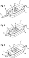
- the in the Fig. 1 to 5 Device shown comprises a housing 1. Within the housing 1, a support plate 2 is arranged, on the surface of which a plurality of electrical contact elements 3 are arranged. Each of these contact elements 3 is connected to a signal line 4, which are led out through an opening on one side of the housing 1 from this.
- the signal lines 4 may, for example, lead to a measuring device (not shown) via which a functional test of a printed circuit board 5 is to take place. For the functional test is provided to contact the printed circuit board 5 defined with the contact elements 3, so that each of the contact elements 3 a e predetermined position on one of Conductors of the circuit board 5 contacted.
- one end of the printed circuit board 5 is inserted into a receptacle 6 which is formed by a receiving element 7 arranged inside the housing 1.
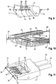
- the receiving element 7, which is preferably made of plastic, comprises two parts (cf. Fig. 5 ), the receptacle 6 and a resiliently connected mounting plate 8, which is fixed immovably within the housing 1.
- the receptacle 6 is designed so that it at least partially encloses the inserted therein portion of the circuit board 5 on five sides (plug-side end, top, both side surfaces and bottom) and in particular leaves free only a portion on its underside, on which the to be contacted interconnects are located.
- the circuit board 5 is inserted so far into the receiving slot formed by the receptacle 6 until its end abuts the bottom of the receiving slot.
- the device further comprises an actuating element in the form of a slider 9.
- the slider 9 forms a survey 10, which is guided in a corresponding recess of the housing 1. By means of the elevation 10, the slider 9 can be moved manually in the directions defined by the recess of the housing 1. Parallel grooves in the surface of the survey 10 ensure sufficient slip resistance when the slide is operated, for example, with the thumb of one hand.
- the circuit board 5 is first positioned exactly to the contact elements 3 by several s pitz tapered positioning pins (not shown) in corresponding positioning holes of the circuit board 5 (see. Fig. 1 ) intervene. Only after the intervention of the positioning pins in the positioning and the resulting positioning of the circuit board 5, ie after a further pivoting of the receptacle 6 and the recorded portion of the circuit board 5, contacting the arranged on the underside of the circuit board 5 interconnects with the contact elements 3. This ensures that the contacting takes place exactly at the intended positions of the tracks.
- the frictional fixing of the slide 9 is effected by the friction which prevails between contact surfaces of the slide 9 and associated contact surfaces of the housing 1 and the receiving element 7.
- This friction can readily be chosen so large that the desired non-positive fixation is achieved, since the slider 9 is clamped by the resilient loading of the receptacle 6 between this and the housing 1.
- This resilient load not only results from the deformation of the connection of the receptacle 6 to the mounting plate 8, but in addition from restoring forces that transmit the contact elements 3 on the circuit board 5 and this in turn on the receptacle 6.
- the contact elements 3 can be resiliently mounted or in the form of spring contact pins, in which at least two parts against the bias of a spring element (in particular telescopically) are mutually displaceable, be formed.
- the contact elements 3 may be formed, for example, as conventional coplanar LIGA contacts. If, on the other hand, a transfer of direct current takes place, the contacts may in particular be conventional Fe derromeroche. Of course, a combination of different contact elements (e.g., LIGA contacts and spring contact pins) may also be used.
- the in the Fig. 6 to 13 illustrated embodiment of a device according to the invention comprises a two-part housing.
- a main body 11 (second housing part) of the housing is part of a lower part of the device.
- a cover 12 (first housing part) of the housing is part of an upper part of the device.
- Base body 11 and lid 12 are pivotally connected to each other via two cylindrical dowel pins 13.
- the main body 11 of the housing forms a receiving recess, in which two (electrically conductive) RF contact elements 14 are arranged.
- the RF contact elements 14 are formed as coplanar contact elements made of metal and each comprise a center contact part 15 and two laterally adjacent to the center contact part 15 arranged outer contact parts 16 in coplanar alignment.
- Their position relative to one another is secured by two respective insulation bodies 17 which are fastened to the RF contact elements 14 in the vicinity of the cable end (for example by gluing).
- the HF contact elements 14 are connected to the base body 11 of the housing (for example adhesively bonded).
- the contact points of the HF contact elements 14 formed on the contact-side end can be in contact with associated contact points of a printed circuit board 18 to be tested (cf. Fig. 8 ) Dodge spring loaded. This provides for a defined contact pressure and for one Tolerance compensation.
- the RF contact elements 14 are each connected to a coaxial cable 19.
- an end tapered inner conductor 20 of each coaxial cable 19 contacts the center contact part 15 of the associated RF contact elements 14, while the two outer contact parts 16 of each of the RF contact elements 14 (via the electrically conductive base body 11) with an outer conductor 39 of the associated coaxial cable 19 electrically are conductively connected.
- High-frequency signals are to be transmitted between the printed circuit board 18 and a measuring device (not shown) via the HF contact elements 14 and the coaxial cables 19.
- a measuring device not shown
- the main body 11 of the housing in an electrically conductive manner, for example made of metal or else of a metallised (for example metallic coated) plastic.
- the design of the RF contact elements 14 as KoplanarKeyimplantation and the transmission by means of the coaxial cable 19 contributes to a good shielding of the high-frequency signals.
- the main body 11 also comprises two positioning pins 21, which engage in associated positioning openings 22 of the printed circuit board 18 in order to position them exactly in the device and to fix them therein. Different diameters of the two positioning pins / positioning pairs ensure that the printed circuit board 18 is inserted into the device in the correct orientation.
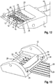
- the lower part of the device further comprises a spring element in the form of a spring comb 23 (see. Fig. 11 ).
- This has a base body, via which the spring comb 23 is fixed to the base body 11 of the housing.
- a plurality of spring fingers 24 extend from the base body.
- the spring comb 23 is intended to ensure reliable contacting of the printed circuit board 18 with contact regions (DC contact elements) formed by the upper part of the device.
- Two lateral support arms 25 prevent tilting of the spring comb 23 at a load of the spring fingers 24.
- the spring comb 23 may advantageously be formed of plastic.
- the cover 12 of the housing forms a receptacle 26 for the printed circuit board 18.
- Two lateral guide slots 27 lead the insertion and withdrawal movement of the printed circuit board 18.
- a flex board 28 (flat conductor) protrudes with one of its ends into the receptacle 26.
- the end contact areas (DC contact elements 30) form. These should contact the associated contact areas of printed conductors 31 of the printed circuit board 18.
- the cover 12 of the housing can therefore also advantageously be made of plastic (for example thermoplastic).
- the flexplate 28 has positioning openings for its positioning and fixing, in which positioning pins 32 of the cover 12 protrude.
- the attachment of the flex board 28 to the cover 12 is also carried out by a distortion between the lid 12 and a spring element 33 with the interposition of an elastomeric element 34.
- the connection of these elements with the lid 12 can be done for example by formed by the lid 12 rivet dome 35, which extend through attachment openings of the spring element 33.
- the free ends of the rivet domes 35 can then be deformed thermally or by pressure, thereby increasing their diameter in the end region. This results in a positive connection with the spring element 33.
- the deformation of the rivet mandrel 35 takes place with simultaneous application of pressure to the spring element 33 and consequent compression of the elastomeric element 34, which remains at least partially upright after forming the rivet mandrel 35.
- the housing or the device In the assembled state of the device acts as a leg spring spring element 33, the housing or the device in its closed position (first rotational position), as shown for example in the Fig. 1 is shown. In this position, the circuit board 18 can not be inserted into the receptacle 26, since the positioning pins 21 protrude into the receptacle 26.
- the housing can be relieved.
- the spring element 33 then moves the two housing parts back into their closed position and holds (fixes) it in this position.
- the positioning pins 21 of the lower part engage in the positioning openings 22 of the printed circuit board 18.
- the printed circuit board 18 is thereby accurately positioned and fixed in the device.
- Two stop pins 36 rest against the printed circuit board 18 and thus limit the elastic deformation of the RF contact elements 14, whereby their damage can be avoided.
- the RF contact elements 14 protrude beyond the stop pins 36 by a defined amount.
- the elastically deformed by the closing of the device spring fingers 24 of the spring comb 23 provide for a sufficient contact pressure and a tolerance compensation.
- a spring finger 24 is provided per DC contact pair. This can ensure that each DC contact pair loaded even with a flexible support plate 38 of the circuit board 18 with the required contact pressure and for each individual tolerance compensation is achieved.
- a corresponding functionality can also be achieved by a (not shown) spring element as a substitute for the spring comb 23 having a common spring body (eg in the form of a leg spring), wherein on the circuit board 18 facing edge (as a continuous pressure edge) individual contact knobs an elastic material are applied.
- the spring body can then provide substantially for the contact pressure, while the contact knobs ensure the individual tolerance compensation.
Description
Die Erfindung betrifft eine Vorrichtung zur Kontaktierung einer Leiterplatte, die zumindest temporär mit beispielsweise einem Messgerät oder einer beliebigen Schaltung verbunden werden soll gemäß dem Oberbegriff von Anspruch 1.The invention relates to a device for contacting a printed circuit board, which is to be connected at least temporarily with, for example, a measuring device or any circuit according to the preamble of claim 1.
Derzeit ist bekannt, solche Leiterplatten durch das Aufstecken eines oder mehrerer Konnektorköpfe zu kontaktieren, was jedoch regelmäßig mit dem Nachteil einer relativ großen Steckkraft verbunden ist, die im Wesentlichen aus der mechanischen Verriegelung der Konnektorköpfe mittels Federelementen resultiert. Eine Kontaktierung mittels Konnektorköpfen ist daher zumindest bei Leiterplatten mit flexibler Trägerplatte ungeeignet. Durch das Stecken der einzelnen Konnektorköpfe können zudem Fehlsteckungen erfolgen, wodurch Beschädigungen der Leiterplatte oder des damit verbundenen elektrischen Systems einhergehen können.At present, it is known to contact such circuit boards by plugging one or more connector heads, which, however, is regularly associated with the disadvantage of a relatively large insertion force, which essentially results from the mechanical locking of the connector heads by means of spring elements. A contact by Konnektorköpfen is therefore unsuitable, at least for printed circuit boards with flexible support plate. By plugging the individual Konnektorköpfe also incorrect connections can be made, which may be accompanied by damage to the circuit board or the associated electrical system.
Die Druckschrift
Die Druckschrift
Ausgehend von diesem Stand der Technik lag der Erfindung die Aufgabe zugrunde, eine Vorrichtung anzugeben, die ein einfaches, schnelles Kontaktieren einer Leiterplatte ermöglicht und insbesondere den Einsatz hoher Steck- bzw. Kontaktkräfte vermeidet, so dass eine Beschädigung der Leiterplatte auch dann vermieden werden kann, wenn die Leiterplatte auf einer flexiblen Trägerplatte aufbaut.Based on this prior art, the present invention seeks to provide a device that allows a simple, fast contacting a circuit board and in particular avoids the use of high plug or contact forces, so that damage to the circuit board can be avoided even then when the circuit board is built on a flexible carrier plate.
Diese Aufgabe wird durch eine Vorrichtung gemäß dem unabhängigen Anspruch 1 gelöst. Vorteilhafte Ausführungsformen der erfindungsgemäßen Vorrichtung sind Gegenstand der abhängigen Ansprüche und ergeben sich aus der nachfolgenden Beschreibung der Erfindung.This object is achieved by a device according to independent claim 1. Advantageous embodiments of the device according to the invention are the subject of the dependent claims and will become apparent from the following description of the invention.
Der Erfindung liegt der Gedanke zugrunde, eine Leiterplatte schnell, einfach, sicher und insbesondere unter Einwirkung geringer Kontaktkräfte mit Gegenkontakten zu kontaktieren, indem die Leiterplatte bzw. der entsprechende zu kontaktierende Abschnitt der Leiterplatte zunächst in einer Aufnahme fixiert und dann durch ein geführtes Bewegen bzw. Verschieben der Leiterplatte bzw. des relevanten Abschnitts, vorzugsweise fixiert in der Aufnahme, ein Kontaktieren von Leiterplatte und Kontaktelementen bewirkt wird.The invention is based on the idea to contact a circuit board quickly, easily, safely and in particular under the action of low contact forces with mating contacts by first fixed the circuit board or the corresponding portion to be contacted the circuit board in a receptacle and then by a guided movement or Moving the circuit board or the relevant portion, preferably fixed in the receptacle, contacting of printed circuit board and contact elements is effected.
Dementsprechend umfasst eine erfindungsgemäße Vorrichtung zur Kontaktierung einer Leiterplatte zumindest folgende Elemente:
- ein oder mehrere HF-Kontaktelemente zur Übertragung von Hochfrequenzsignalen, die vorzugsweise unbeweglich positioniert in der Vorrichtung und insbesondere innerhalb eines (Teils eines) Gehäuses der Vorrichtung angeordnet sind;
- (mindestens) eine Aufnahme, in die zumindest ein Abschnitt der Leiterplatte steckbar ist; die Aufnahme umgreift die Leiterplatte bzw. den Abschnitt der Leiterplatte vorzugsweise möglichst großflächig und lässt insbesondere lediglich den Abschnitt der Leiterplatten frei, auf dem diejenigen (Abschnitte der) Leiterbahnen angeordnet sind, die kontaktiert werden sollen;
- Mittel zum Bewegen der Leiterplatte relativ zu den Kontaktelementen bis zu einem Kontaktieren mit den Kontaktelementen; durch das geführte Bewegen der Leiterplatte wird sichergestellt, dass sich diese definiert auf die Kontaktelemente zubewegt, wodurch Fehlkontaktierungen ausgeschlossen werden und zudem ein Verkanten der Leiterplatte relativ zu den Kontaktelementen vermieden werden kann, das mit höheren Kontaktkräften einhergehen könnte; und
- Mittel zum Fixieren der Leiterplatte in der die Kontaktelemente kontaktierenden Position, wodurch die dauerhafte Kontaktierung sichergestellt werden kann.
- one or more RF contact elements for transmitting radio-frequency signals, which are preferably arranged immovably positioned in the device and in particular within a (part of) a housing of the device;
- (At least) a receptacle into which at least a portion of the circuit board is pluggable; the receptacle preferably surrounds the printed circuit board or the section of the printed circuit board over as large a surface as possible and, in particular, exposes only the section of the printed circuit boards on which those (sections of) interconnects to be contacted are arranged;
- Means for moving the circuit board relative to the contact elements until contacting with the contact elements; the guided movement of the printed circuit board ensures that it moves toward the contact elements in a defined manner, thereby precluding misconnections and, moreover, avoiding tilting of the printed circuit board relative to the contact elements, which could be accompanied by higher contact forces; and
- Means for fixing the circuit board in the contact elements contacting position, whereby the permanent contact can be ensured.
In einer bevorzugten Ausführungsform der erfindungsgemäßen Vorrichtung ist vorgesehen, dass die Vorrichtung weiterhin (mindestens) ein Zentrierelement aufweist, durch das die Leiterplatte noch vor dem Kontaktieren der Kontaktelemente zentriert wird. Dies erfolgt vorzugsweise durch das geführte Bewegen bzw. Verschieben der Leiterplatte relativ zu den Kontaktelementen.In a preferred embodiment of the device according to the invention it is provided that the device further comprises (at least) a centering element, through which the circuit board is centered before contacting the contact elements. This is preferably done by the guided movement or displacement of the printed circuit board relative to the contact elements.
Beispielsweise kann (mindestens) ein (vorzugsweise sich in zumindest einem Abschnitt verjüngender) Zentrierstift vorgesehen sein, auf den eine Öffnung der Leiterplatte aufgeschoben wird, wodurch diese zentriert wird. Dadurch kann sichergestellt werden, dass die Leiterbahnen der Leiterplatte exakt zu den dazugehörigen Kontaktelementen ausgerichtet werden.For example, (at least) one (preferably tapered in at least one section) centering be provided on which an opening of the circuit board is pushed, whereby it is centered. This can ensure that the conductor tracks of the printed circuit board are aligned exactly with the associated contact elements.
Besonders bevorzugt können mindestens zwei Zentrierstifte vorgesehen sein, die sich hinsichtlich ihrer Form, Anordnung und/oder Dimensionierung unterscheiden und in entsprechend angeordnete und/oder dimensionierte Öffnungen der Leiterplatte eingreifen können. Dadurch kann eine Kodierung geschaffen werden, die ein falsches Einsetzen der Leiterplatte verhindern kann.Particularly preferably, at least two centering pins can be provided, which differ with respect to their shape, arrangement and / or dimensioning and can engage in correspondingly arranged and / or dimensioned openings of the printed circuit board. As a result, a coding can be created that can prevent incorrect insertion of the circuit board.
Vorzugsweise kann vorgesehen sein, dass die Leiterplatte zusammen mit der Aufnahme bewegt bzw. verschoben wird, um die Kontaktelemente zu kontaktieren. Dadurch besteht die Möglichkeit, die für das Bewegen aufzubringenden Kräfte auf die Aufnahme und nicht auf die Leiterplatte auszuüben. Die Übertragung dieser Kräfte von der Aufnahme auf die Leiterplatte kann dann über eine relativ große Fläche und folglich mit geringerem Druck erfolgen.Preferably, it can be provided that the circuit board is moved or moved together with the receptacle to contact the contact elements. As a result, it is possible to apply the forces to be applied for moving to exercise the recording and not on the circuit board. The transmission of these forces from the recording on the circuit board can then take place over a relatively large area and consequently with less pressure.
Weiterhin bevorzugt kann vorgesehen sein, dass die Aufnahme federnd gelagert ist. Dadurch kann zum einen erreicht werden, dass die Aufnahme im unbelasteten Zustand, d.h. wenn diese von den Mitteln zum Verschieben nicht mit einer eine Bewegung hervorrufenden Kraft beaufschlagt ist, von der federnden Lagerung in eine Ausgangslage beaufschlagt wird, in der die Leiterplatte die Kontaktelemente nicht kontaktiert. Dadurch kann sichergestellt werden, dass die Leiterplatte bei einem Einstecken in die Aufnahme noch keinen Kontakt zu den Kontaktelementen herstellt. Das Verschieben der Leiterplatte einschließlich der Aufnahme mit dem Ziel einer Kontaktierung der Kontaktelemente kann dann entgegen der Reaktionskraft der federnden Lagerung der Aufnahme erfolgen. Die dabei erzeugte Federvorspannung kann zudem dazu verwendet werden, die Leiterplatte in der die Kontaktelemente kontaktierenden Stellung (Kontaktstellung) zu fixieren.Further preferably, it can be provided that the receptacle is resiliently mounted. This can be achieved on the one hand, that the recording in the unloaded state, i. if it is not acted upon by the means for moving with a force causing a movement, is acted upon by the resilient mounting in an initial position in which the circuit board does not contact the contact elements. This can ensure that the circuit board does not make contact with the contact elements when plugged into the receptacle. The displacement of the printed circuit board including the receptacle with the aim of contacting the contact elements can then take place counter to the reaction force of the resilient mounting of the recording. The spring preload generated thereby can also be used to fix the circuit board in the contact elements contacting position (contact position).
Die erfindungsgemäße Vorrichtung weist ein Gehäuse mit einem ersten, die Aufnahme ausbildenden Gehäuseteil und einem zweiten, die Kontaktelemente umfassenden Gehäuseteil auf, wobei die beiden Gehäuseteile zueinander drehbar sind. Die beiden Gehäuseteile sind dabei derart miteinander verbunden, dass in einer ersten Drehstellung eine in die Aufnahme gesteckte Leiterplatte die Kontaktelemente kontaktieren würde bzw. kontaktiert und in einer zweiten Drehstellung eine in die Aufnahme gesteckte Leiterplatte die Kontaktelemente nicht kontaktieren würde bzw. kontaktiert.Weiterhin sind die beiden Gehäuseteile mittels eines Federelements in die erste Drehstellung beaufschlagt. Für ein Einstecken der Leiterplatte würden die beiden Gehäuseteile dann relativ zueinander in die zweite Drehstellung verdreht (z.B. manuell), so dass ein Einstecken der Leiterplatte ohne Kontaktierung der Kontaktelemente erfolgen kann. Ein Entlasten der beiden Gehäuseteile kann dann dazu führen, dass die beiden Gehäuseteile infolge der Federbelastung selbsttätig in die erste Drehstellung bewegt werden und in dieser durch die Federbelastung fixiert sind.The device according to the invention has a housing with a first housing part forming the receptacle and a second housing part comprising the contact elements, wherein the two housing parts are rotatable relative to one another. The two housing parts are connected to each other such that in a first rotational position inserted into the recording circuit board would contact the contact elements and contacted and in a second rotational position inserted into the recording circuit board contact elements would not contact or kontaktiert.Weiterhin are the both housing parts acted upon by means of a spring element in the first rotational position. For insertion of the printed circuit board, the two housing parts would then rotated relative to each other in the second rotational position (eg manually), so that insertion of the circuit board without contacting the contact elements can be done. Relieving the two housing parts can then cause the two housing parts are automatically moved due to the spring load in the first rotational position and are fixed in this by the spring load.
Da ein Einstecken der Leiterplatte in die Aufnahme in der ersten Drehstellung die Kontaktelemente und/oder die Leiterplatte beschädigen könnte, kann weiterhin bevorzugt vorgesehen sein, dass Mittel, die ein Einstecken der Leiterplatte in die Aufnahme in der ersten Drehstellung verhindern, vorgesehen sind. Bei diesen Mitteln kann es sich vorzugsweise um den oder die Zentrierstifte handeln, die in der ersten Drehstellung in einem Einführschlitz der Aufnahme angeordnet sind und dadurch ein Einstecken der Leiterplatte in die Aufnahme verhindern.Since plugging the printed circuit board into the receptacle in the first rotational position could damage the contact elements and / or the printed circuit board, it can furthermore preferably be provided that means which prevent insertion of the printed circuit board into the receptacle in the first rotational position are provided. These means may preferably be the one or more centering pins, which are arranged in the first rotational position in an insertion slot of the receptacle and thereby prevent insertion of the circuit board into the receptacle.
In einer weiterhin bevorzugten Ausgestaltung der erfindungsgemäßen Vorrichtung kann mindestens ein DC-Kontaktelement zur Übertragung von Gleichstrom vorgesehen sein. Dabei kann das HF-Kontaktelement vorteilhafterweise einen Mittelkontaktteil umfassen, der koplanar zwischen zwei Außenkontaktteilen angeordnet ist.In a further preferred embodiment of the device according to the invention, at least one DC contact element can be provided for the transmission of direct current. In this case, the HF contact element may advantageously comprise a center contact part which is arranged coplanar between two outer contact parts.
Da sich Koaxialkabel vorteilhaft zur Übertragung von Hochfrequenzsignalen eignen, kann weiterhin bevorzugt vorgesehen sein, dass der Mittelkontaktteil mit einem Innenleiter und die Außenkontaktteile mit einem Außenleiter eines von der Vorrichtung abgehenden Koaxialkabels elektrisch verbunden sind. Mittels des Koaxialkabels kann die Vorrichtung bzw. können das oder die HF-Kontaktelemente beispielsweise mit einer Messvorrichtung verbunden sein.Since coaxial cables are advantageously suitable for the transmission of high-frequency signals, it may furthermore be preferred for the center contact part to be electrically connected to an inner conductor and the outer contact parts to be electrically connected to an outer conductor of a coaxial cable which leaves the device. By means of the coaxial cable, the device or the RF contact element (s) can be connected, for example, to a measuring device.
Vorteilhafterweise kann dagegen das DC-Kontaktelement mit einem von der Vorrichtung abgehenden, vorzugsweise flexiblen Flachleiter elektrisch verbunden sein. Dieser kann sich durch geringe Kosten und einen geringen Platzbedarf auszeichnen. Eine direkte Kontaktierung auf eine oder mehrere Kupferlitzen ist ebenfalls möglich.Advantageously, on the other hand, the DC contact element can be electrically connected to a preferably flat flexible conductor which leads away from the device. This can be characterized by low costs and a small footprint. A direct contact with one or more copper strands is also possible.
Durch die Kontaktierung der Leiterplatte mit den Kontaktelementen der erfindungsgemäßen Vorrichtung sollen insbesondere Hochfrequenzsignale (HF-Signale) übertragen werden.By contacting the circuit board with the contact elements of the device according to the invention in particular high-frequency signals (RF signals) are to be transmitted.
Die Erfindung wird nachfolgend anhand von in den Zeichnungen dargestellten Ausführungsbeispielen näher erläutert. In den Zeichnungen zeigt:
- Fig. 1 bis Fig. 3:
- verschiedene Schritte bei der Verwendung einer nicht beanspruchten Vorrichtung zur Kontaktierung einer Leiterplatte;
- Fig. 4:
- einen Abschnitt der Vorrichtung gemäß den
Fig. 1 bis 3 in einem isometrischen Längsschnitt; - Fig. 5:
- ein Aufnahmeelement der Vorrichtung gemäß den
Fig. 1 bis 4 in einer isometrischen Darstellung; - Fig. 6:
- eine erste Ausführungsform einer erfindungsgemäßen Vorrichtung (ohne Leiterplatte) im geschlossenen Zustand in einer perspektivischen Darstellung;
- Fig. 7:
- die Vorrichtung gemäß
Fig. 6 im geschlossenen Zustand; - Fig. 8:
- eine Leiterplatte zur Verwendung mit der Vorrichtung gemäß den
Fig. 6 und 7 in einer perspektivischen Darstellung; - Fig. 9:
- die Vorrichtung gemäß den
Fig. 6 und 7 mit teilweise eingesteckter Leiterplatte gemäßFig. 8 in einer perspektivischen Darstellung; - Fig. 10:
- einen perspektivischen Längsschnitt durch die Vorrichtung gemäß der
Fig. 9 mit vollständig eingesteckter Leiterplatte; - Fig. 11:
- ein Unterteil der Vorrichtung gemäß den
Fig. 6 und 7 in einer perspektivischen Darstellung; - Fig. 12:
- das Unterteil gemäß der
Fig. 10 mit integriertem Kontaktfederkamm; und - Fig. 13:
- ein Oberteil der Vorrichtung gemäß den
Fig. 6 und 7 in einer perspektivischen Darstellung.
- Fig. 1 to Fig. 3:
- various steps in the use of an unclaimed device for contacting a printed circuit board;
- 4:
- a portion of the device according to the
Fig. 1 to 3 in an isometric longitudinal section; - Fig. 5:
- a receiving element of the device according to the
Fig. 1 to 4 in an isometric view; - Fig. 6:
- a first embodiment of a device according to the invention (without circuit board) in the closed state in a perspective view;
- Fig. 7:
- the device according to
Fig. 6 when closed; - Fig. 8:
- a printed circuit board for use with the device according to the
6 and 7 in a perspective view; - Fig. 9:
- the device according to the
6 and 7 with partially inserted circuit board according toFig. 8 in a perspective view; - Fig. 10:
- a perspective longitudinal section through the device according to the
Fig. 9 with fully inserted circuit board; - Fig. 11:
- a lower part of the device according to the
6 and 7 in a perspective view; - Fig. 12:
- the lower part according to the
Fig. 10 with integrated contact spring comb; and - Fig. 13:
- an upper part of the device according to the
6 and 7 in a perspective view.
Die in den
Für die Kontaktierung mit den Kontaktelementen 3 wird ein Ende der Leiterplatte 5 in eine Aufnahme 6 eingeschoben, die von einem innerhalb des Gehäuses 1 angeordneten Aufnahmeelement 7 ausgebildet ist. Das vorzugsweise aus Kunststoff gefertigte Aufnahmeelement 7 umfasst zwei Teile (vgl. insbesondere
Die Vorrichtung umfasst zudem noch ein Betätigungselement in Form eines Schiebers 9. Der Schieber 9 bildet eine Erhebung 10 aus, die in einer entsprechenden Aussparung des Gehäuses 1 geführt ist. Mittels der Erhebung 10 kann der Schieber 9 manuell in den durch die Aussparung des Gehäuses 1 definierten Richtungen bewegt werden. Parallel verlaufende Nuten in der Oberfläche der Erhebung 10 sorgen dabei für eine ausreichende Rutschfestigkeit, wenn der Schieber beispielsweise mit dem Daumen einer Hand betätigt wird.The device further comprises an actuating element in the form of a
Beim Bewegen des Schiebers 9 gleitet dieser auf der Oberseite der Aufnahmeplatte 7. Durch ein Bewegen des Schiebers 9 ausgehend von der in den
Im Verlauf dieser Bewegung wird die Leiterplatte 5 zunächst exakt zu den Kontaktelementen 3 positioniert, indem mehrere s pitz zulaufende Positionierstifte (nicht dargestellt) in entsprechende Positionieröffnungen der Leiterplatte 5 (vgl.
In der in der
Die kraftschlüssige Fixierung des Schiebers 9 erfolgt durch die Reibung, die zwischen Kontaktflächen des Schiebers 9 und dazugehörigen Kontaktflächen des Gehäuses 1 bzw. des Aufnahmeelements 7 herrscht. Diese Reibung kann ohne Weiteres so groß gewählt werden, dass die gewünschte kraftschlüssige Fixierung erreicht wird, da der Schieber 9 durch die federnde Belastung der Aufnahme 6 zwischen dieser und dem Gehäuse 1 verspannt ist. Diese federnde Belastung resultiert nicht nur aus der Deformation der Anbindung der Aufnahme 6 an die Befestigungsplatte 8, sondern zusätzlich aus Rückstellkräften, die die Kontaktelemente 3 auf die Leiterplatte 5 und diese wiederum auf die Aufnahme 6 übertragen. Hierzu können die Kontaktelemente 3 federnd gelagert oder in Form von Federkontaktstiften, bei denen zumindest zwei Teile entgegen der Vorspannung eines Federelements (insbesondere teleskopartig) zueinander verschiebbar sind, ausgebildet sein.The frictional fixing of the
Sofern mittels der Kontaktierung von Leiterplatte 5 und Kontaktelementen 3 HF-Signale übertragen werden sollen, können die Kontaktelemente 3 beispielsweise als konventionelle koplanare LIGA-Kontakte ausgebildet sein. Soll dagegen eine Übertragung von Gleichstrom erfolgen, kann es sich bei den Kontakten insbesondere um konventionelle Fe derkontaktstifte handeln. Selbstverständlich kann auch eine Kombination verschiedener Kontaktelemente (z.B. LIGA-Kontakte und Federkontaktstifte) zum Einsatz kommen.If 3 HF signals are to be transmitted by means of the contacting of printed circuit board 5 and contact elements, the
Die in den
Der Grundkörper 11 des Gehäuses bildet eine Aufnahmevertiefung aus, in der zwei (elektrisch leitfähige) HF-Kontaktelemente 14 angeordnet sind. Die HF-Kontaktelemente 14 sind als Koplanarkontaktelemente aus Metall ausgebildet und umfassen jeweils ein Mittelkontaktteil 15 sowie zwei seitlich neben dem Mittelkontaktteil 15 angeordnete Außenkontaktteile 16 in koplanarer Ausrichtung. Die Mittel- 15 und Außenkontaktteile 16, die beispielsweise mittels eines sogenannten LIGA-Verfahrens hergestellt worden sein können, bilden zwischen sich elektrisch isolierenden Luftspalte aus. Ihre Position zueinander ist durch jeweils zwei Isolationskörper 17 gesichert, die in der Nähe des kabelseitigen Endes an den HF-Kontaktelementen 14 befestigt (z.B. durch Verkleben) sind. Mittels jeweils eines der Isolationskörper 17 sind die HF-Kontaktelemente 14 mit dem Grundkörper 11 des Gehäuses verbunden (z.B. verklebt).The
Der Abschnitt der HF-Kontaktelemente 14, der sich zwischen ihrem jeweiligen kontaktseitigen Ende und den dazugehörigen Isolationskörpern 17 befindet, ragt frei in den Raum. Dadurch können die am kontaktseitigen Ende ausgebildeten Kontaktstellen der HF-Kontaktelemente 14 bei einem Kontakt mit dazugehörigen Kontaktstellen einer zu testenden Leiterplatte 18 (vgl.
Am ihren kabelseitigen Enden sind die HF-Kontaktelemente 14 jeweils mit einem Koaxialkabel 19 verbunden. Hierzu kontaktiert ein endseitig spitz zulaufender Innenleiter 20 jedes Koaxialkabels 19 den Mittelkontaktteil 15 des dazugehörigen HF-Kontaktelemente 14, während die beiden Außenkontaktteile 16 jedes der HF-Kontaktelemente 14 (über den elektrisch leitfähig ausgebildeten Grundkörper 11) mit einem Außenleiter 39 des dazugehörigen Koaxialkabels 19 elektrisch leitend verbunden sind.At their cable-side ends, the
Über die HF-Kontaktelemente 14 sowie die Koaxialkabel 19 sollen Hochfrequenzsignale zwischen der Leiterplatte 18 und einer nicht dargestellten Messvorrichtung übertragen werden. Für eine gute Abschirmung der Hochfrequenzsignale ist vorgesehen, den Grundkörper 11 des Gehäuses elektrisch leitend auszubilden, beispielsweise aus Metall oder auch aus einem metallisierten (z.B. metallisch beschichteten) Kunststoff. Auch die Ausgestaltung der HF-Kontaktelemente 14 als Koplanarkontaktelemente sowie die Übertragung mittels der Koaxialkabel 19 trägt zu einer guten Abschirmung der Hochfrequenzsignale bei.High-frequency signals are to be transmitted between the printed
Der Grundkörper 11 umfasst noch zwei Positionierzapfen 21, die in dazugehörige Positionieröffnungen 22 der Leiterplatte 18 eingreifen, um diese exakt in der Vorrichtung zu positionieren sowie darin zu fixieren. Unterschiedliche Durchmesser der beiden Positionierzapfen/Positionieröffnungen-Paare stellen sicher, dass die Leiterplatte 18 in der richtigen Ausrichtung in die Vorrichtung eingesetzt wird.The
Das Unterteil der Vorrichtung umfasst weiterhin noch ein Federelement in Form eines Federkamms 23 (vgl.
Der Deckel 12 des Gehäuses bildet eine Aufnahme 26 für die Leiterplatte 18 aus. Zwei seitliche Führungsschlitze 27 führen dabei die Einsteck- und Herausziehbewegung der Leiterplatte 18. Eine Flexplatine 28 (Flachleiter) ragt mit einem seiner Enden in die Aufnahme 26. Auf der dem Unterteil bzw. der eingesteckten Leiterplatte 18 zugewandten Seite der Flexplatine 28 sind mehrere Leiterbahnen 29 angeordnet, die endseitig Kontaktbereiche (DC-Kontaktelemente 30) ausbilden. Diese sollen mit dazugehörigen Kontaktbereichen von Leiterbahnen 31 der Leiterplatte 18 kontaktieren. Über die Leiterbahnen 29, 31 sollen im Betrieb der Vorrichtung lediglich Gleichströme übertragen werden, so dass kein Aufwand für eine Abschirmung getroffen werden muss. Der Deckel 12 des Gehäuses kann daher auch vorteilhaft aus Kunststoff (z.B. Thermoplast) ausgebildet sein. Die Flexplatine 28 weist zu ihrer Positionierung und Fixierung Positionieröffnungen auf, in die Positionierzapfen 32 des Deckels 12 ragen. Die Befestigung der Flexplatine 28 an dem Deckel 12 erfolgt zudem durch ein Verspannen zwischen dem Deckel 12 sowie einem Federelement 33 unter Zwischenschaltung eines Elastomerelements 34. Die Verbindung dieser Elemente mit dem Deckel 12 kann beispielsweise durch von dem Deckel 12 ausgebildete Nietdome 35 erfolgen, die sich durch Befestigungsöffnungen des Federelements 33 erstrecken. Die freien Enden der Nietdome 35 können dann thermisch oder durch Druck verformt werden, wodurch deren Durchmesser im Endbereich vergrößert wird. Dadurch ergibt sich eine formschlüssige Verbindung mit dem Federelement 33. Vorzugsweise erfolgt das Verformen der Nietdome 35 bei gleichzeitiger Druckausübung auf das Federelement 33 und einer dadurch bedingten Kompression des Elastomerelements 34, die nach dem Umformen der Nietdome 35 zumindest teilweise aufrecht gehalten bleibt. Dadurch ergibt sich eine weitgehend spielfreie Befestigung der Flexplatine 28 an dem Deckel 12.The
Im montierten Zustand der Vorrichtung beaufschlagt das als Schenkelfeder ausgebildete Federelement 33 das Gehäuse bzw. die Vorrichtung in seine/ihre geschlossene Stellung (erste Drehstellung), wie dies z.B. in der
Ein Einschieben der Leiterplatte 18 in die Aufnahme 26 ist lediglich in der in der
Nach einem vollständigen Einschieben der Leiterplatte 18 kann das Gehäuse entlastet werden. Das Federelement 33 bewegt die beiden Gehäuseteile dann wieder in ihre geschlossene Stellung und hält (fixiert) es in dieser Stellung. Dabei greifen die Positionierzapfen 21 des Unterteils in die Positionieröffnungen 22 der Leiterplatte 18. Die Leiterplatte 18 ist dadurch in der Vorrichtung exakt positioniert sowie fixiert. Gleichzeitig kontaktieren die HF-Kontaktelemente 14 entsprechende HF-Kontaktstellen 38 an der Unterseite der Leiterplatte 18, wobei dabei die HF-Kontaktelemente 14 geringfügig elastisch deformiert werden, um einen ausreichenden Kontaktdruck und Toleranzausgleich zu erzeugen. Zwei Anschlagzapfen 36 liegen dabei an der Leiterplatte 18 an und begrenzen somit die elastische Verformung der HF-Kontaktelemente 14, wodurch deren Beschädigung vermieden werden kann Dazu ragen die HF-Kontaktelemente 14 um ein definiertes Maß über die Anschlagzapfen 36 hinaus. Ebenso kontaktieren die DC-Kontaktelemente 30 der Flexplatine 28 die dazugehörigen Leiterbahnen 31 auf der Oberseite der Leiterplatte 18 (DC-Kontaktpaare). Die durch das Schließen der Vorrichtung elastisch deformierten Federfinger 24 des Federkamms 23 sorgen dabei für einen ausreichenden Kontaktdruck und einen Toleranzausgleich. Im vorliegenden Ausführungsbeispiel ist je DC-Kontaktpaar ein Federfinger 24 vorgesehen. Dadurch kann sichergestellt werden, dass jedes DC-Kontaktpaar auch bei einer flexiblen Trägerplatte 38 der Leiterplatte 18 mit dem benötigten Kontaktdruck belastet und für jedes ein individueller Toleranzausgleich erreicht wird.After a complete insertion of the
Eine entsprechende Funktionalität kann auch durch ein (nicht gezeigtes) Federelement als Ersatz für den Federkamm 23 erreicht werden, das einen gemeinsamen Federgrundkörper (z.B. in Form einer Schenkelfeder) aufweist, wobei auf der der Leiterplatte 18 zugewandten Kante (als durchgehende Andrückkante) einzelne Kontaktnoppen aus einem elastischen Material aufgebracht sind. Der Federgrundkörper kann dann im Wesentlichen für den Kontaktdruck sorgen, während die Kontaktnoppen den individuellen Toleranzausgleich sicherstellen.A corresponding functionality can also be achieved by a (not shown) spring element as a substitute for the
Claims (12)
- Device for contacting a circuit board (18) comprising- one or more HF contact elements (14), for the transmission of high frequency signals,- an intake (26) into which at least one section of the circuit board (18) can be inserted,- a housing comprising a first housing part forming the intake (26) and a second housing part containing at least one of the contact elements (14), whereby the two housing parts can be moved relative to one another,- means for moving the intake (26) together with the circuit board (18) relative to the contact elements (14) until the contact elements (14) are contacted, and- means for fixing the circuit board (18) in the position in which the contact elements (14) are contacted,whereby the two housing parts can rotate relative to one another, whereby in a first rotary position a circuit board (18) plugged into the intake (26) contacts the contact elements (14) and in a second rotary position the circuit board (18) plugged into the intake (26) does not contact the contact elements (14), characterised in that the two housing parts are biased in the first rotary position by means of a spring element (33).
- Device according to claim 1, characterised in that on being moved the circuit board (18) is centred before contacting the contact elements (14).
- Device according to claim 2, characterised through a centring pin (21) onto which an opening in the circuit board (18) is pushed.
- Device according to claim 3, characterised through at least two centring pins (21) which differ in their form and/or dimensioning.
- Device according to one of the preceding claims, characterised in that the intake (26) is spring-mounted.
- Device according to one of the preceding claims, characterised through means which prevent the circuit board (18) from being plugged into the intake (26) in the first rotary position.
- Device according to claims 3 or 4 and 6, characterised in that the centring pin or pins (21) prevent the circuit board (18) from being plugged into the intake (26) in the first rotary position.
- Device according to one of the preceding claims, characterised through at least one DC contact element (30) for the transmission of direct current.
- Device according to one of the preceding claims, characterised in that the HF contact element (14) comprises a central contact part (15) which is arranged in coplanar alignment between two outer contact parts (16).
- Device according to claim 9, characterised in that the central contact part (15) is electrically connected with an inner conductor (20) and the outer contact parts (16) are electrically connected with an outer conductor of a coaxial cable (19) leading away from the device.
- Device according to claim 8, characterised in that the DC contact element (30) is electrically connected with a ribbon conductor leading away from the device.
- System which includes a device according to one of the preceding claims and a circuit board (18).
Applications Claiming Priority (2)
| Application Number | Priority Date | Filing Date | Title |
|---|---|---|---|
| DE202012001645U DE202012001645U1 (en) | 2012-02-17 | 2012-02-17 | Device for contacting a printed circuit board |
| PCT/EP2013/000214 WO2013120580A1 (en) | 2012-02-17 | 2013-01-24 | Device for contacting a circuit board |
Publications (2)
| Publication Number | Publication Date |
|---|---|
| EP2815462A1 EP2815462A1 (en) | 2014-12-24 |
| EP2815462B1 true EP2815462B1 (en) | 2018-08-08 |
Family
ID=47632970
Family Applications (1)
| Application Number | Title | Priority Date | Filing Date |
|---|---|---|---|
| EP13702340.4A Active EP2815462B1 (en) | 2012-02-17 | 2013-01-24 | Device for contacting a printed circuit |
Country Status (10)
| Country | Link |
|---|---|
| US (1) | US9240643B2 (en) |
| EP (1) | EP2815462B1 (en) |
| JP (1) | JP6254537B2 (en) |
| KR (1) | KR101901743B1 (en) |
| CN (1) | CN104115336B (en) |
| CA (1) | CA2876631C (en) |
| DE (1) | DE202012001645U1 (en) |
| HK (1) | HK1201993A1 (en) |
| TW (1) | TWM462374U (en) |
| WO (1) | WO2013120580A1 (en) |
Families Citing this family (7)
| Publication number | Priority date | Publication date | Assignee | Title |
|---|---|---|---|---|
| US9568499B2 (en) * | 2013-11-22 | 2017-02-14 | Tektronix, Inc. | High performance LIGA spring interconnect system for probing application |
| US9142903B2 (en) | 2013-11-22 | 2015-09-22 | Tektronix, Inc. | High performance multiport connector system using LIGA springs |
| CN104319505B (en) * | 2014-11-17 | 2018-01-19 | 合肥京东方光电科技有限公司 | Flexible printed circuit board grafting tool |
| JP6821918B2 (en) * | 2016-02-18 | 2021-01-27 | 大日本印刷株式会社 | Light guide plate and display device |
| US10847912B2 (en) | 2018-03-19 | 2020-11-24 | Rohde & Schwarz Gmbh & Co. Kg | Broadband socket connector, broadband plug connector, and system thereof |
| TWI718610B (en) * | 2018-08-09 | 2021-02-11 | 日商歐姆龍股份有限公司 | Probe unit |
| CN114778902B (en) * | 2022-06-27 | 2022-11-11 | 武汉永鼎光通科技有限公司 | PCBA adds electric testing arrangement and prevents crossing anchor clamps of inserting |
Citations (1)
| Publication number | Priority date | Publication date | Assignee | Title |
|---|---|---|---|---|
| EP0131410A2 (en) * | 1983-07-06 | 1985-01-16 | Tokyo Tatsuno Company Limited | Device for reading and writing IC-external storage card |
Family Cites Families (18)
| Publication number | Priority date | Publication date | Assignee | Title |
|---|---|---|---|---|
| FR1174063A (en) | 1957-03-30 | 1959-03-05 | Electrical terminal couplers | |
| FR2492213A1 (en) * | 1980-10-15 | 1982-04-16 | Labo Electronique Physique | Reader for plastic transaction or data cards with tilt locking - uses sleeve into which card is inserted and electromagnet to allow sleeve to tip so card is trapped and positioned against reader |
| JPS5972753U (en) * | 1982-11-04 | 1984-05-17 | 株式会社東芝 | Attached equipment |
| JPS59187162U (en) * | 1983-05-30 | 1984-12-12 | 三菱電機株式会社 | printed wiring board equipment |
| JPS6022795A (en) * | 1983-07-18 | 1985-02-05 | Tokyo Tatsuno Co Ltd | Reading and writing device of plate-shaped memory medium |
| US4700997A (en) * | 1986-11-14 | 1987-10-20 | Minnesota Mining And Manufacturing Company | Electrical connector |
| GB2235078B (en) * | 1989-08-19 | 1993-09-08 | Technophone Ltd | Card reader |
| US6447305B1 (en) * | 1996-05-14 | 2002-09-10 | Miraco, Inc. | Circuit to printed circuit board stored energy connector |
| JP2000277218A (en) * | 1999-03-19 | 2000-10-06 | Ace Five:Kk | Cable assembly |
| US6447317B1 (en) * | 2001-07-11 | 2002-09-10 | Hon Hai Precision Ind. Co., Ltd. | Backplane connector |
| US6623312B2 (en) * | 2001-10-04 | 2003-09-23 | Unilead International | Precordial electrocardiogram electrode connector |
| JP3976276B2 (en) * | 2005-06-10 | 2007-09-12 | 日本航空電子工業株式会社 | Inspection device |
| JP4558588B2 (en) * | 2005-06-14 | 2010-10-06 | 第一電子工業株式会社 | connector |
| JP2008135209A (en) * | 2006-11-27 | 2008-06-12 | Fujifilm Corp | Clip-type connector |
| JP4908374B2 (en) * | 2007-10-17 | 2012-04-04 | 日本航空電子工業株式会社 | Connector device |
| JP5436088B2 (en) * | 2008-08-19 | 2014-03-05 | 矢崎総業株式会社 | Flexible aggregation wiring connector |
| US20100105230A1 (en) * | 2008-10-23 | 2010-04-29 | Sony Ericsson Mobile Communications Ab | Connector |
| JP5410872B2 (en) * | 2009-07-27 | 2014-02-05 | モレックス インコーポレイテド | Hybrid connector |
-
2012
- 2012-02-17 DE DE202012001645U patent/DE202012001645U1/en not_active Expired - Lifetime
-
2013
- 2013-01-24 KR KR1020147026013A patent/KR101901743B1/en active IP Right Grant
- 2013-01-24 EP EP13702340.4A patent/EP2815462B1/en active Active
- 2013-01-24 CN CN201380009752.8A patent/CN104115336B/en active Active
- 2013-01-24 JP JP2014556943A patent/JP6254537B2/en active Active
- 2013-01-24 CA CA2876631A patent/CA2876631C/en active Active
- 2013-01-24 US US14/379,033 patent/US9240643B2/en active Active
- 2013-01-24 WO PCT/EP2013/000214 patent/WO2013120580A1/en active Application Filing
- 2013-02-18 TW TW102203123U patent/TWM462374U/en not_active IP Right Cessation
-
2015
- 2015-03-10 HK HK15102439.8A patent/HK1201993A1/en not_active IP Right Cessation
Patent Citations (1)
| Publication number | Priority date | Publication date | Assignee | Title |
|---|---|---|---|---|
| EP0131410A2 (en) * | 1983-07-06 | 1985-01-16 | Tokyo Tatsuno Company Limited | Device for reading and writing IC-external storage card |
Also Published As
| Publication number | Publication date |
|---|---|
| US20150024619A1 (en) | 2015-01-22 |
| CA2876631C (en) | 2018-04-10 |
| JP2015507341A (en) | 2015-03-05 |
| CN104115336B (en) | 2017-02-22 |
| CA2876631A1 (en) | 2013-08-22 |
| JP6254537B2 (en) | 2017-12-27 |
| DE202012001645U1 (en) | 2013-05-21 |
| EP2815462A1 (en) | 2014-12-24 |
| KR101901743B1 (en) | 2018-09-28 |
| CN104115336A (en) | 2014-10-22 |
| US9240643B2 (en) | 2016-01-19 |
| HK1201993A1 (en) | 2015-09-11 |
| WO2013120580A1 (en) | 2013-08-22 |
| KR20140125442A (en) | 2014-10-28 |
| TWM462374U (en) | 2013-09-21 |
Similar Documents
| Publication | Publication Date | Title |
|---|---|---|
| EP2815462B1 (en) | Device for contacting a printed circuit | |
| DE2845234C2 (en) | ||
| EP2037536A2 (en) | Connection terminal | |
| WO1997043886A1 (en) | Electrical connector | |
| EP2983255B1 (en) | Jack for telecommunication and/or data transmission systems | |
| EP3482465B1 (en) | Spring-loaded inner-conductor contact element | |
| EP0150327B1 (en) | Contact device | |
| DE102007017059B4 (en) | Socket for electrical components | |
| EP3286805B1 (en) | Plug system having low-wear contacting | |
| DE102011110637B4 (en) | Connectors | |
| EP1249895B1 (en) | Electrical connector | |
| DE112012001361T5 (en) | connector device | |
| DE102010034975A1 (en) | Electronic circuit for e.g. transmission and/or receiving device in motor car, has printed circuit boards held by fixing pins that are arranged in housing, where fixing pins include set of layers that is arranged corresponding to boards | |
| DE19944909A1 (en) | Electrical connection unit for electrically driven system, esp. positional measurement system, has first and second electrical contacts connected together in pairs | |
| EP3076188B1 (en) | Test contactor, method and use | |
| EP1761975A1 (en) | Coaxial plug-in connector comprising a contact mechanism for electrical contact | |
| WO2021191061A1 (en) | Electrical connection device and method for mounting an electrical connection device | |
| DE112021001561T5 (en) | Floating header and PCB assembly | |
| WO2004032589A1 (en) | Electronic appliance comprising a floating circuit carrier | |
| WO1999014995A1 (en) | Electrical device with an adjusting element | |
| EP3605746A1 (en) | Plug connector and connection with such a connector | |
| DE4327986C2 (en) | Coaxial connector | |
| EP2562885B1 (en) | Connector with a spring member for electric direct contacting of a circuit board | |
| EP0578099A1 (en) | Coaxial plug connector component | |
| EP2078964A1 (en) | Connector contact, IC test socket and method |
Legal Events
| Date | Code | Title | Description |
|---|---|---|---|
| PUAI | Public reference made under article 153(3) epc to a published international application that has entered the european phase |
Free format text: ORIGINAL CODE: 0009012 |
|
| 17P | Request for examination filed |
Effective date: 20140731 |
|
| AK | Designated contracting states |
Kind code of ref document: A1 Designated state(s): AL AT BE BG CH CY CZ DE DK EE ES FI FR GB GR HR HU IE IS IT LI LT LU LV MC MK MT NL NO PL PT RO RS SE SI SK SM TR |
|
| AX | Request for extension of the european patent |
Extension state: BA ME |
|
| DAX | Request for extension of the european patent (deleted) | ||
| 17Q | First examination report despatched |
Effective date: 20151211 |
|
| GRAP | Despatch of communication of intention to grant a patent |
Free format text: ORIGINAL CODE: EPIDOSNIGR1 |
|
| STAA | Information on the status of an ep patent application or granted ep patent |
Free format text: STATUS: GRANT OF PATENT IS INTENDED |
|
| RIC1 | Information provided on ipc code assigned before grant |
Ipc: H01R 12/77 20110101ALN20180309BHEP Ipc: H01R 11/24 20060101ALN20180309BHEP Ipc: H01R 12/81 20110101AFI20180309BHEP |
|
| INTG | Intention to grant announced |
Effective date: 20180326 |
|
| GRAS | Grant fee paid |
Free format text: ORIGINAL CODE: EPIDOSNIGR3 |
|
| GRAA | (expected) grant |
Free format text: ORIGINAL CODE: 0009210 |
|
| STAA | Information on the status of an ep patent application or granted ep patent |
Free format text: STATUS: THE PATENT HAS BEEN GRANTED |
|
| AK | Designated contracting states |
Kind code of ref document: B1 Designated state(s): AL AT BE BG CH CY CZ DE DK EE ES FI FR GB GR HR HU IE IS IT LI LT LU LV MC MK MT NL NO PL PT RO RS SE SI SK SM TR |
|
| REG | Reference to a national code |
Ref country code: GB Ref legal event code: FG4D Free format text: NOT ENGLISH |
|
| REG | Reference to a national code |
Ref country code: CH Ref legal event code: EP Ref country code: AT Ref legal event code: REF Ref document number: 1028062 Country of ref document: AT Kind code of ref document: T Effective date: 20180815 |
|
| REG | Reference to a national code |
Ref country code: IE Ref legal event code: FG4D Free format text: LANGUAGE OF EP DOCUMENT: GERMAN |
|
| REG | Reference to a national code |
Ref country code: DE Ref legal event code: R096 Ref document number: 502013010773 Country of ref document: DE |
|
| REG | Reference to a national code |
Ref country code: NL Ref legal event code: FP |
|
| REG | Reference to a national code |
Ref country code: LT Ref legal event code: MG4D |
|
| PG25 | Lapsed in a contracting state [announced via postgrant information from national office to epo] |
Ref country code: FI Free format text: LAPSE BECAUSE OF FAILURE TO SUBMIT A TRANSLATION OF THE DESCRIPTION OR TO PAY THE FEE WITHIN THE PRESCRIBED TIME-LIMIT Effective date: 20180808 Ref country code: LT Free format text: LAPSE BECAUSE OF FAILURE TO SUBMIT A TRANSLATION OF THE DESCRIPTION OR TO PAY THE FEE WITHIN THE PRESCRIBED TIME-LIMIT Effective date: 20180808 Ref country code: PL Free format text: LAPSE BECAUSE OF FAILURE TO SUBMIT A TRANSLATION OF THE DESCRIPTION OR TO PAY THE FEE WITHIN THE PRESCRIBED TIME-LIMIT Effective date: 20180808 Ref country code: GR Free format text: LAPSE BECAUSE OF FAILURE TO SUBMIT A TRANSLATION OF THE DESCRIPTION OR TO PAY THE FEE WITHIN THE PRESCRIBED TIME-LIMIT Effective date: 20181109 Ref country code: BG Free format text: LAPSE BECAUSE OF FAILURE TO SUBMIT A TRANSLATION OF THE DESCRIPTION OR TO PAY THE FEE WITHIN THE PRESCRIBED TIME-LIMIT Effective date: 20181108 Ref country code: SE Free format text: LAPSE BECAUSE OF FAILURE TO SUBMIT A TRANSLATION OF THE DESCRIPTION OR TO PAY THE FEE WITHIN THE PRESCRIBED TIME-LIMIT Effective date: 20180808 Ref country code: RS Free format text: LAPSE BECAUSE OF FAILURE TO SUBMIT A TRANSLATION OF THE DESCRIPTION OR TO PAY THE FEE WITHIN THE PRESCRIBED TIME-LIMIT Effective date: 20180808 Ref country code: IS Free format text: LAPSE BECAUSE OF FAILURE TO SUBMIT A TRANSLATION OF THE DESCRIPTION OR TO PAY THE FEE WITHIN THE PRESCRIBED TIME-LIMIT Effective date: 20181208 Ref country code: NO Free format text: LAPSE BECAUSE OF FAILURE TO SUBMIT A TRANSLATION OF THE DESCRIPTION OR TO PAY THE FEE WITHIN THE PRESCRIBED TIME-LIMIT Effective date: 20181108 |
|
| PG25 | Lapsed in a contracting state [announced via postgrant information from national office to epo] |
Ref country code: HR Free format text: LAPSE BECAUSE OF FAILURE TO SUBMIT A TRANSLATION OF THE DESCRIPTION OR TO PAY THE FEE WITHIN THE PRESCRIBED TIME-LIMIT Effective date: 20180808 Ref country code: AL Free format text: LAPSE BECAUSE OF FAILURE TO SUBMIT A TRANSLATION OF THE DESCRIPTION OR TO PAY THE FEE WITHIN THE PRESCRIBED TIME-LIMIT Effective date: 20180808 Ref country code: LV Free format text: LAPSE BECAUSE OF FAILURE TO SUBMIT A TRANSLATION OF THE DESCRIPTION OR TO PAY THE FEE WITHIN THE PRESCRIBED TIME-LIMIT Effective date: 20180808 |
|
| PG25 | Lapsed in a contracting state [announced via postgrant information from national office to epo] |
Ref country code: ES Free format text: LAPSE BECAUSE OF FAILURE TO SUBMIT A TRANSLATION OF THE DESCRIPTION OR TO PAY THE FEE WITHIN THE PRESCRIBED TIME-LIMIT Effective date: 20180808 Ref country code: CZ Free format text: LAPSE BECAUSE OF FAILURE TO SUBMIT A TRANSLATION OF THE DESCRIPTION OR TO PAY THE FEE WITHIN THE PRESCRIBED TIME-LIMIT Effective date: 20180808 Ref country code: RO Free format text: LAPSE BECAUSE OF FAILURE TO SUBMIT A TRANSLATION OF THE DESCRIPTION OR TO PAY THE FEE WITHIN THE PRESCRIBED TIME-LIMIT Effective date: 20180808 Ref country code: EE Free format text: LAPSE BECAUSE OF FAILURE TO SUBMIT A TRANSLATION OF THE DESCRIPTION OR TO PAY THE FEE WITHIN THE PRESCRIBED TIME-LIMIT Effective date: 20180808 |
|
| REG | Reference to a national code |
Ref country code: DE Ref legal event code: R097 Ref document number: 502013010773 Country of ref document: DE |
|
| PG25 | Lapsed in a contracting state [announced via postgrant information from national office to epo] |
Ref country code: DK Free format text: LAPSE BECAUSE OF FAILURE TO SUBMIT A TRANSLATION OF THE DESCRIPTION OR TO PAY THE FEE WITHIN THE PRESCRIBED TIME-LIMIT Effective date: 20180808 Ref country code: SK Free format text: LAPSE BECAUSE OF FAILURE TO SUBMIT A TRANSLATION OF THE DESCRIPTION OR TO PAY THE FEE WITHIN THE PRESCRIBED TIME-LIMIT Effective date: 20180808 Ref country code: SM Free format text: LAPSE BECAUSE OF FAILURE TO SUBMIT A TRANSLATION OF THE DESCRIPTION OR TO PAY THE FEE WITHIN THE PRESCRIBED TIME-LIMIT Effective date: 20180808 |
|
| PLBE | No opposition filed within time limit |
Free format text: ORIGINAL CODE: 0009261 |
|
| STAA | Information on the status of an ep patent application or granted ep patent |
Free format text: STATUS: NO OPPOSITION FILED WITHIN TIME LIMIT |
|
| 26N | No opposition filed |
Effective date: 20190509 |
|
| PG25 | Lapsed in a contracting state [announced via postgrant information from national office to epo] |
Ref country code: MC Free format text: LAPSE BECAUSE OF FAILURE TO SUBMIT A TRANSLATION OF THE DESCRIPTION OR TO PAY THE FEE WITHIN THE PRESCRIBED TIME-LIMIT Effective date: 20180808 Ref country code: SI Free format text: LAPSE BECAUSE OF FAILURE TO SUBMIT A TRANSLATION OF THE DESCRIPTION OR TO PAY THE FEE WITHIN THE PRESCRIBED TIME-LIMIT Effective date: 20180808 |
|
| REG | Reference to a national code |
Ref country code: CH Ref legal event code: PL |
|
| PG25 | Lapsed in a contracting state [announced via postgrant information from national office to epo] |
Ref country code: LU Free format text: LAPSE BECAUSE OF NON-PAYMENT OF DUE FEES Effective date: 20190124 |
|
| REG | Reference to a national code |
Ref country code: IE Ref legal event code: MM4A |
|
| PG25 | Lapsed in a contracting state [announced via postgrant information from national office to epo] |
Ref country code: LI Free format text: LAPSE BECAUSE OF NON-PAYMENT OF DUE FEES Effective date: 20190131 Ref country code: CH Free format text: LAPSE BECAUSE OF NON-PAYMENT OF DUE FEES Effective date: 20190131 |
|
| PG25 | Lapsed in a contracting state [announced via postgrant information from national office to epo] |
Ref country code: IE Free format text: LAPSE BECAUSE OF NON-PAYMENT OF DUE FEES Effective date: 20190124 |
|
| PG25 | Lapsed in a contracting state [announced via postgrant information from national office to epo] |
Ref country code: TR Free format text: LAPSE BECAUSE OF FAILURE TO SUBMIT A TRANSLATION OF THE DESCRIPTION OR TO PAY THE FEE WITHIN THE PRESCRIBED TIME-LIMIT Effective date: 20180808 |
|
| PG25 | Lapsed in a contracting state [announced via postgrant information from national office to epo] |
Ref country code: MT Free format text: LAPSE BECAUSE OF FAILURE TO SUBMIT A TRANSLATION OF THE DESCRIPTION OR TO PAY THE FEE WITHIN THE PRESCRIBED TIME-LIMIT Effective date: 20180808 Ref country code: PT Free format text: LAPSE BECAUSE OF FAILURE TO SUBMIT A TRANSLATION OF THE DESCRIPTION OR TO PAY THE FEE WITHIN THE PRESCRIBED TIME-LIMIT Effective date: 20181208 |
|
| PG25 | Lapsed in a contracting state [announced via postgrant information from national office to epo] |
Ref country code: CY Free format text: LAPSE BECAUSE OF FAILURE TO SUBMIT A TRANSLATION OF THE DESCRIPTION OR TO PAY THE FEE WITHIN THE PRESCRIBED TIME-LIMIT Effective date: 20180808 |
|
| PG25 | Lapsed in a contracting state [announced via postgrant information from national office to epo] |
Ref country code: HU Free format text: LAPSE BECAUSE OF FAILURE TO SUBMIT A TRANSLATION OF THE DESCRIPTION OR TO PAY THE FEE WITHIN THE PRESCRIBED TIME-LIMIT; INVALID AB INITIO Effective date: 20130124 |
|
| PG25 | Lapsed in a contracting state [announced via postgrant information from national office to epo] |
Ref country code: MK Free format text: LAPSE BECAUSE OF FAILURE TO SUBMIT A TRANSLATION OF THE DESCRIPTION OR TO PAY THE FEE WITHIN THE PRESCRIBED TIME-LIMIT Effective date: 20180808 |
|
| PGFP | Annual fee paid to national office [announced via postgrant information from national office to epo] |
Ref country code: FR Payment date: 20230124 Year of fee payment: 11 Ref country code: AT Payment date: 20230118 Year of fee payment: 11 |
|
| PGFP | Annual fee paid to national office [announced via postgrant information from national office to epo] |
Ref country code: IT Payment date: 20230120 Year of fee payment: 11 Ref country code: GB Payment date: 20230124 Year of fee payment: 11 Ref country code: DE Payment date: 20230127 Year of fee payment: 11 Ref country code: BE Payment date: 20230124 Year of fee payment: 11 |
|
| P01 | Opt-out of the competence of the unified patent court (upc) registered |
Effective date: 20230524 |
|
| PGFP | Annual fee paid to national office [announced via postgrant information from national office to epo] |
Ref country code: NL Payment date: 20230124 Year of fee payment: 11 |
|
| REG | Reference to a national code |
Ref country code: DE Ref legal event code: R082 Ref document number: 502013010773 Country of ref document: DE Representative=s name: KANDLBINDER, MARKUS, DIPL.-PHYS., DE |
|
| PGFP | Annual fee paid to national office [announced via postgrant information from national office to epo] |
Ref country code: NL Payment date: 20240125 Year of fee payment: 12 |