JP6254537B2 - Device for contacting circuit boards - Google Patents
Device for contacting circuit boards Download PDFInfo
- Publication number
- JP6254537B2 JP6254537B2 JP2014556943A JP2014556943A JP6254537B2 JP 6254537 B2 JP6254537 B2 JP 6254537B2 JP 2014556943 A JP2014556943 A JP 2014556943A JP 2014556943 A JP2014556943 A JP 2014556943A JP 6254537 B2 JP6254537 B2 JP 6254537B2
- Authority
- JP
- Japan
- Prior art keywords
- circuit board
- contact
- intake
- contact element
- housing
- Prior art date
- Legal status (The legal status is an assumption and is not a legal conclusion. Google has not performed a legal analysis and makes no representation as to the accuracy of the status listed.)
- Active
Links
- 239000004020 conductor Substances 0.000 claims description 16
- 230000005540 biological transmission Effects 0.000 claims description 9
- 238000003780 insertion Methods 0.000 description 11
- 230000037431 insertion Effects 0.000 description 11
- 238000012937 correction Methods 0.000 description 5
- 210000003811 finger Anatomy 0.000 description 4
- 239000002184 metal Substances 0.000 description 4
- 229910052751 metal Inorganic materials 0.000 description 4
- 239000004033 plastic Substances 0.000 description 4
- 229920001971 elastomer Polymers 0.000 description 3
- 239000000806 elastomer Substances 0.000 description 3
- 239000012212 insulator Substances 0.000 description 3
- 238000004026 adhesive bonding Methods 0.000 description 2
- 238000000034 method Methods 0.000 description 2
- RYGMFSIKBFXOCR-UHFFFAOYSA-N Copper Chemical compound [Cu] RYGMFSIKBFXOCR-UHFFFAOYSA-N 0.000 description 1
- 230000001154 acute effect Effects 0.000 description 1
- 230000006835 compression Effects 0.000 description 1
- 238000007906 compression Methods 0.000 description 1
- 229910052802 copper Inorganic materials 0.000 description 1
- 239000010949 copper Substances 0.000 description 1
- 230000001419 dependent effect Effects 0.000 description 1
- 238000013461 design Methods 0.000 description 1
- 230000005489 elastic deformation Effects 0.000 description 1
- 239000013013 elastic material Substances 0.000 description 1
- 238000000605 extraction Methods 0.000 description 1
- 239000006260 foam Substances 0.000 description 1
- 238000011990 functional testing Methods 0.000 description 1
- 238000012360 testing method Methods 0.000 description 1
- 229920001169 thermoplastic Polymers 0.000 description 1
- 239000004416 thermosoftening plastic Substances 0.000 description 1
- 210000003813 thumb Anatomy 0.000 description 1
Images


Classifications
-
- H—ELECTRICITY
- H01—ELECTRIC ELEMENTS
- H01R—ELECTRICALLY-CONDUCTIVE CONNECTIONS; STRUCTURAL ASSOCIATIONS OF A PLURALITY OF MUTUALLY-INSULATED ELECTRICAL CONNECTING ELEMENTS; COUPLING DEVICES; CURRENT COLLECTORS
- H01R12/00—Structural associations of a plurality of mutually-insulated electrical connecting elements, specially adapted for printed circuits, e.g. printed circuit boards [PCB], flat or ribbon cables, or like generally planar structures, e.g. terminal strips, terminal blocks; Coupling devices specially adapted for printed circuits, flat or ribbon cables, or like generally planar structures; Terminals specially adapted for contact with, or insertion into, printed circuits, flat or ribbon cables, or like generally planar structures
- H01R12/70—Coupling devices
- H01R12/82—Coupling devices connected with low or zero insertion force
- H01R12/83—Coupling devices connected with low or zero insertion force connected with pivoting of printed circuits or like after insertion
-
- H—ELECTRICITY
- H01—ELECTRIC ELEMENTS
- H01R—ELECTRICALLY-CONDUCTIVE CONNECTIONS; STRUCTURAL ASSOCIATIONS OF A PLURALITY OF MUTUALLY-INSULATED ELECTRICAL CONNECTING ELEMENTS; COUPLING DEVICES; CURRENT COLLECTORS
- H01R12/00—Structural associations of a plurality of mutually-insulated electrical connecting elements, specially adapted for printed circuits, e.g. printed circuit boards [PCB], flat or ribbon cables, or like generally planar structures, e.g. terminal strips, terminal blocks; Coupling devices specially adapted for printed circuits, flat or ribbon cables, or like generally planar structures; Terminals specially adapted for contact with, or insertion into, printed circuits, flat or ribbon cables, or like generally planar structures
- H01R12/70—Coupling devices
- H01R12/77—Coupling devices for flexible printed circuits, flat or ribbon cables or like structures
- H01R12/81—Coupling devices for flexible printed circuits, flat or ribbon cables or like structures connecting to another cable except for flat or ribbon cable
-
- H—ELECTRICITY
- H01—ELECTRIC ELEMENTS
- H01R—ELECTRICALLY-CONDUCTIVE CONNECTIONS; STRUCTURAL ASSOCIATIONS OF A PLURALITY OF MUTUALLY-INSULATED ELECTRICAL CONNECTING ELEMENTS; COUPLING DEVICES; CURRENT COLLECTORS
- H01R13/00—Details of coupling devices of the kinds covered by groups H01R12/70 or H01R24/00 - H01R33/00
- H01R13/64—Means for preventing incorrect coupling
-
- H—ELECTRICITY
- H01—ELECTRIC ELEMENTS
- H01R—ELECTRICALLY-CONDUCTIVE CONNECTIONS; STRUCTURAL ASSOCIATIONS OF A PLURALITY OF MUTUALLY-INSULATED ELECTRICAL CONNECTING ELEMENTS; COUPLING DEVICES; CURRENT COLLECTORS
- H01R4/00—Electrically-conductive connections between two or more conductive members in direct contact, i.e. touching one another; Means for effecting or maintaining such contact; Electrically-conductive connections having two or more spaced connecting locations for conductors and using contact members penetrating insulation
- H01R4/28—Clamped connections, spring connections
- H01R4/48—Clamped connections, spring connections utilising a spring, clip, or other resilient member
-
- H—ELECTRICITY
- H01—ELECTRIC ELEMENTS
- H01R—ELECTRICALLY-CONDUCTIVE CONNECTIONS; STRUCTURAL ASSOCIATIONS OF A PLURALITY OF MUTUALLY-INSULATED ELECTRICAL CONNECTING ELEMENTS; COUPLING DEVICES; CURRENT COLLECTORS
- H01R11/00—Individual connecting elements providing two or more spaced connecting locations for conductive members which are, or may be, thereby interconnected, e.g. end pieces for wires or cables supported by the wire or cable and having means for facilitating electrical connection to some other wire, terminal, or conductive member, blocks of binding posts
- H01R11/11—End pieces or tapping pieces for wires, supported by the wire and for facilitating electrical connection to some other wire, terminal or conductive member
- H01R11/22—End pieces terminating in a spring clip
- H01R11/24—End pieces terminating in a spring clip with gripping jaws, e.g. crocodile clip
-
- H—ELECTRICITY
- H01—ELECTRIC ELEMENTS
- H01R—ELECTRICALLY-CONDUCTIVE CONNECTIONS; STRUCTURAL ASSOCIATIONS OF A PLURALITY OF MUTUALLY-INSULATED ELECTRICAL CONNECTING ELEMENTS; COUPLING DEVICES; CURRENT COLLECTORS
- H01R12/00—Structural associations of a plurality of mutually-insulated electrical connecting elements, specially adapted for printed circuits, e.g. printed circuit boards [PCB], flat or ribbon cables, or like generally planar structures, e.g. terminal strips, terminal blocks; Coupling devices specially adapted for printed circuits, flat or ribbon cables, or like generally planar structures; Terminals specially adapted for contact with, or insertion into, printed circuits, flat or ribbon cables, or like generally planar structures
- H01R12/70—Coupling devices
- H01R12/77—Coupling devices for flexible printed circuits, flat or ribbon cables or like structures
- H01R12/771—Details
- H01R12/774—Retainers
-
- H—ELECTRICITY
- H01—ELECTRIC ELEMENTS
- H01R—ELECTRICALLY-CONDUCTIVE CONNECTIONS; STRUCTURAL ASSOCIATIONS OF A PLURALITY OF MUTUALLY-INSULATED ELECTRICAL CONNECTING ELEMENTS; COUPLING DEVICES; CURRENT COLLECTORS
- H01R2201/00—Connectors or connections adapted for particular applications
- H01R2201/20—Connectors or connections adapted for particular applications for testing or measuring purposes
Description
本発明は、例えば測定装置又は何らかの種類の回路に接続されるべき回路基板を、少なくとも一時的に、接触させるための装置に関する。 The present invention relates to a device for contacting, for example at least temporarily, a circuit board to be connected to a measuring device or some kind of circuit, for example.
現在、1つ以上のコネクタヘッドを差し込むことにより、このような回路基板が接触されることは周知であるが、これは概して、比較的大きい差し込み力を必要とするという短所と関連しており、この差し込み力は、実質的に、スプリング要素を用いることにより、コネクタヘッドのメカニカルロックから結果的に生じるものである。したがって、少なくとも可撓性キャリアプレートを有する回路基板の事例では、コネクタヘッドを用いることによる接触は不向きである。また、回路基板へのダメージ、又はこれに接続される電気システムへのダメージにつながり得る接続エラーが、個々のコネクタヘッドを差し込むことで結果的に生じる可能性がある。 Currently, it is well known that such circuit boards are brought into contact by inserting one or more connector heads, but this is generally associated with the disadvantage of requiring a relatively large insertion force, This insertion force results essentially from the mechanical locking of the connector head by using a spring element. Therefore, in the case of a circuit board having at least a flexible carrier plate, contact using a connector head is unsuitable. Also, connection errors that can lead to damage to the circuit board or damage to the electrical system connected to it can result from the insertion of individual connector heads.
この先行技術を出発点として、本発明は、回路基板の簡単かつ迅速な接触を可能にし、高い差し込み力又は接触力の付加を特に回避するため、回路基板が可撓性キャリアプレートに基づく場合でも回路基板へのダメージが回避されることが可能な装置を特徴付けるという問題に基づくものであった。 Starting from this prior art, the present invention enables simple and quick contact of the circuit board, and especially avoids the application of high insertion force or contact force, even when the circuit board is based on a flexible carrier plate. It was based on the problem of characterizing a device capable of avoiding damage to the circuit board.
この問題は、独立請求項1に記載の装置により解決される。本発明による装置の有利な実施形態は、従属請求項の主題であり、本発明についての以下の記載で説明される。 This problem is solved by the device according to independent claim 1. Advantageous embodiments of the device according to the invention are the subject matter of the dependent claims and are explained in the following description of the invention.
本発明は、接触されるべき回路基板又は回路基板の対応するセクションがインテークに固定されてから、好ましくはインテークに固定される回路基板又は関連するセクションの案内動作又は摺動により回路基板と接触要素との接触がもたらされることで、迅速かつ確実に、特に低接触力の付加により回路基板と適合接点とを接触させるという概念に基づいている。 The invention relates to a circuit board and a contact element by means of a guiding action or sliding of the circuit board or the associated section which is preferably fixed to the intake after the circuit board or the corresponding section of the circuit board to be contacted is fixed to the intake. Is based on the concept of bringing the circuit board into contact with the matching contact quickly and reliably, in particular with the addition of a low contact force.
したがって、回路基板を接触させるための本発明による装置は、少なくとも以下の要素を含む。
好ましくは、装置に移動不能に位置決めされ、特に装置のハウジング(の一部)の内部に配置される1つ以上の接触要素。
回路基板の少なくとも1つのセクションが挿入することが可能な(少なくとも)1つのインテーク。好ましくはできる限り広いエリアにわたって回路基板又は回路基板のセクションを収納し、特に、接触されるべき回路経路(のセクション)が配置される回路基板のセクションのみを露出した状態にするインテーク。
接触要素との接触が行われるまで、回路基板を接触要素に対して移動又は摺動させるための手段。回路基板の案内動作は、回路基板が定義された方法により接触要素へ移動することを保証し、これは接触エラーを排除し、また高い接触力が使用される際に発生するように回路基板が接触要素に対して傾斜することを防止する。
接触要素が接触している位置に回路基板を固定又は保持して永久接触を保証するための手段。
Accordingly, the device according to the invention for contacting a circuit board comprises at least the following elements:
One or more contact elements which are preferably positioned immovably on the device and in particular arranged inside (part of) the housing of the device.
One (at least) intake into which at least one section of the circuit board can be inserted. Intake, preferably containing a circuit board or a section of the circuit board over as large an area as possible, in particular leaving only the section of the circuit board in which the circuit path to be contacted is located.
Means for moving or sliding the circuit board relative to the contact element until contact with the contact element is made. The guiding action of the circuit board ensures that the circuit board moves to the contact element in a defined way, which eliminates contact errors and also causes the circuit board to occur when high contact forces are used. Prevents tilting with respect to the contact element.
Means for securing or holding the circuit board in a position where the contact element is in contact to assure permanent contact.
本発明による装置の好適な実施形態において、装置は、接触要素に接触する前に回路基板がセンタリングされる(少なくとも)1つのセンタリング要素も備える。これは、好ましくは、接触要素に対する回路基板の案内動作又は摺動により達成される。 In a preferred embodiment of the device according to the invention, the device also comprises (at least) one centering element in which the circuit board is centered before contacting the contact element. This is preferably achieved by a guiding action or sliding of the circuit board relative to the contact element.
例えば、(少なくとも)1つのセンタリングピン(好ましくは、少なくとも1つのセクションにテーパ状のセンタリングピン)が設けられ、回路基板の開口部がこれに押圧されて、回路基板がセンタリングされる。こうして、回路基板の回路経路が対応する接触要素に対して正確に位置合わせされることが保証され得る。 For example, (at least) one centering pin (preferably a tapered centering pin in at least one section) is provided, and the opening of the circuit board is pressed against it, thereby centering the circuit board. In this way it can be ensured that the circuit path of the circuit board is accurately aligned with the corresponding contact element.
形状、配置、及び/又は寸法が異なる、少なくとも2つのセンタリングピンが設けられて、対応する配置及び/又は寸法を持つ回路基板の開口部に嵌合し得ることが特に好ましい。これは、回路基板の不正確な挿入が防止するコーディングを形成することができる。 It is particularly preferred that at least two centering pins with different shapes, arrangements and / or dimensions are provided so that they can be fitted into openings in circuit boards with corresponding arrangements and / or dimensions. This can form a coding that prevents inaccurate insertion of the circuit board.
接触要素に接触するために、回路基板はインテークとともに移動又は摺動することが可能であることが好ましい。これは、移動に必要な力を回路基板ではなくインテークに付加することを可能にする。インテークから回路基板へのこれらの力の伝達は、この時、比較的広い表面エリアにわたって、結果的に低い圧力で実行することが可能である。 The circuit board is preferably capable of moving or sliding with the intake in order to contact the contact element. This allows the force required for movement to be applied to the intake rather than the circuit board. The transmission of these forces from the intake to the circuit board can then be performed over a relatively large surface area and consequently with a low pressure.
インテークは、ばね装着されることも好ましい。これは、一方では、無負荷状態では、つまり力を生じる移動を摺動手段によって受けない時には、インテークは、ばね負荷装着により、回路基板が接触要素と接触しない初期位置へ付勢されることを意味する。こうして、インテークへ差し込まれる際に、回路基板は接触要素との接触をまだ確立していないことを保証することができる。接触要素との接触を目的とするインテークを含めた回路基板の摺動は、この時、インテークのばね負荷装着の反力に抵抗して実行することができる。加えて、結果的に生じるばねの予備張力は、接触要素が接触する位置(接触位置)に回路基板を固定するために使用することができる。 The intake is also preferably spring mounted. On the one hand, this means that the intake is biased to the initial position where the circuit board does not come into contact with the contact element by means of a spring load when there is no load, i.e. when no sliding movement is received by the sliding means. means. Thus, when inserted into the intake, it can be ensured that the circuit board has not yet established contact with the contact element. At this time, the sliding of the circuit board including the intake intended for contact with the contact element can be executed while resisting the reaction force of the intake mounted on the spring load. In addition, the resulting pre-tension of the spring can be used to fix the circuit board in the position where the contact element contacts (contact position).
回路基板の摺動は、好ましくはスライダーを用いることでもたらされ、スライダーの移動方向と回路基板の移動方向とは好ましくは非平行(また非同軸)である。このスライダー及び回路基板の移動の非平行性は、簡単な手段により比較的大きな伝達比を実現するこが可能であるため、初期位置から接触位置への回路基板の好ましくは比較的短い移動をもたらすためには、スライダーの非常に大きな摺動が必要であるという利点を有する。これは、好ましくは手動操作のスライダーの取り扱いを容易にする。 The sliding of the circuit board is preferably effected by using a slider, and the moving direction of the slider and the moving direction of the circuit board are preferably non-parallel (and non-coaxial). This non-parallel nature of the movement of the slider and the circuit board allows a relatively large transmission ratio to be achieved by simple means, and thus preferably results in a relatively short movement of the circuit board from the initial position to the contact position. This has the advantage that a very large slide of the slider is required. This facilitates the handling of the preferably manually operated slider.
スライダーの接触面が回路基板及び/又はインテークの接触面上を摺動することにより、相対移動の方向に関して、接触面が相互に対して0°を超過し(>0°)、且つ90°未満(<90°)となる角度で位置合わせされることで、スライダーと回路基板との非平行移動が簡単な方式で達成することが可能である。これは、「傾斜面」の機能に対応する簡単な方式でスライダー及び回路基板の所望の非平行移動が実現できることを意味する。加えて、2つの移動の伝達比は、接触面の間に形成される角度の選択により簡単に調節することができる。 By sliding the contact surface of the slider on the contact surface of the circuit board and / or the intake, the contact surfaces exceed 0 ° (> 0 °) and less than 90 ° relative to each other in the direction of relative movement. By aligning at an angle of (<90 °), non-parallel movement between the slider and the circuit board can be achieved in a simple manner. This means that the desired non-parallel movement of the slider and the circuit board can be realized in a simple manner corresponding to the function of the “inclined surface”. In addition, the transmission ratio of the two movements can be easily adjusted by selecting the angle formed between the contact surfaces.
さらに、回路基板が接触要素と接触する位置でのスライダーのフォースロック固定が、本実施形態により実現できる。これは、スライダーの移動の結果としての回路基板の移動が、スプリング要素の弾性力に反して行われることで達成できる。この弾性力は、2つの接触面の間の摩擦を増加させ、結果的に、装置の接触位置でのスライダーのフォースロック固定を可能にする。例えば、インテークが回路基板とともに変位される場合には、伸縮弾性力は、インテークのばね負荷装着により付加することができる。代替的又は付加的に、例えば接触要素がばね装着されるか、変形の結果として自身で弾性力を発生させることで、接触要素により付加される弾性力を有するという有利な可能性も存在する。 Furthermore, the force lock fixing of the slider at the position where the circuit board contacts the contact element can be realized by this embodiment. This can be achieved by moving the circuit board as a result of the movement of the slider against the elastic force of the spring element. This elastic force increases the friction between the two contact surfaces, and as a result, enables the force-locking of the slider at the contact position of the device. For example, when the intake is displaced together with the circuit board, the elastic elastic force can be applied by mounting the intake with a spring load. Alternatively or additionally, there is also the advantageous possibility that the contact element has an elastic force added by the contact element, for example by spring mounting or by generating an elastic force itself as a result of deformation.
本発明による装置の好適な実施形態では、インテークを形成する第1ハウジング部品と、接触要素を収納する第2ハウジング部品とを含み、2つのハウジング部品が相互に対して移動することが可能なハウジングを装置が備える。 In a preferred embodiment of the device according to the invention, a housing comprising a first housing part forming an intake and a second housing part containing a contact element, the two housing parts being movable relative to one another The device is equipped with.
2つのハウジング部品は、特に好ましくは、相互に対して回転するように設計され、特に、インテークへ差し込まれた回路基板は第1回転位置で接触要素と接触する又は接触する予定であり、インテークへ差し込まれた回路基板は第2回転位置で接触要素と接触しない又は接触しない予定であるような方式で相互に接続することができる。 The two housing parts are particularly preferably designed to rotate relative to each other, in particular the circuit board inserted into the intake is in contact with or will contact the contact element in the first rotational position. The inserted circuit boards can be connected to each other in such a way that they do not contact or will not contact the contact elements in the second rotational position.
2つのハウジング部品がスプリング要素を用いることにより、第1回転位置に付勢されることも好ましい。回路基板を差し込むため、2つのハウジング部品は、この時、第2回転位置へ(例えば手動で)相互に回転されるため、回路基板は接触要素と接触せずに差し込むことができる。それから、2つのハウジング部品を解放すると、ばね力の結果として2つのハウジング部品が第1回転位置へ自動的に移動して、ばね力を通して第1回転位置に固定される。 It is also preferred that the two housing parts are biased to the first rotational position by using spring elements. To insert the circuit board, the two housing parts are then rotated relative to each other (for example manually) into the second rotational position, so that the circuit board can be inserted without contacting the contact element. Then, when the two housing parts are released, the two housing parts automatically move to the first rotational position as a result of the spring force and are fixed in the first rotational position through the spring force.
第1回転位置で回路基板をインテークへ差し込むと、接触要素及び/又は回路基板にダメージを与えるので、第1回転位置では回路基板がインテークへ差し込まれることを防止する手段も設けられることが好ましい。これらの手段は、好ましくは、第1回転位置でインテークの挿入スロットに配置され、結果的に回路基板がインテークへ差し込まれることを防止する単数又は複数のセンタリングピンで構成することができる。 If the circuit board is inserted into the intake at the first rotational position, the contact element and / or the circuit board is damaged. Therefore, it is preferable to provide means for preventing the circuit board from being inserted into the intake at the first rotational position. These means can preferably consist of one or more centering pins which are arranged in the insertion slot of the intake in the first rotational position and consequently prevent the circuit board from being inserted into the intake.
本発明による装置のさらなる好適な実施形態では、高周波信号の伝送のために少なくとも1つのHF接触要素が設けられ、直流の伝送のために少なくとも1つのDC接触要素を設けることができる。したがって、HF接触要素は、2つの外側接触部の間に共面に位置合わせされた状態で配置される中央接触部を含むので、有利である。 In a further preferred embodiment of the device according to the invention, at least one HF contact element can be provided for the transmission of high-frequency signals and at least one DC contact element for the transmission of direct current. Thus, the HF contact element is advantageous because it includes a central contact portion that is disposed in coplanar alignment between the two outer contact portions.
同軸ケーブルは高周波信号の伝送に適しており有利であるので、中央接触部もまた、好ましくは内側導体と電気的に接続され、外側接触部は装置から延出する同軸ケーブルの外側導体と電気的に接続することができる。装置又はHF接触要素は、例えば、同軸ケーブルを用いることにより、測定装置と接続することができる。 Since the coaxial cable is suitable and advantageous for the transmission of high-frequency signals, the central contact is also preferably electrically connected to the inner conductor and the outer contact is electrically connected to the outer conductor of the coaxial cable extending from the device. Can be connected to. The device or HF contact element can be connected to the measuring device, for example by using a coaxial cable.
対照的に、DC接触要素は、装置から延出する好ましくは可撓性のリボン導体と電気的に接続されると有利である。これらは、低コスト及び低スペース要求により特徴付けられる。1つ以上の銅撚線導体への直接接触も可能である。 In contrast, the DC contact element is advantageously electrically connected with a preferably flexible ribbon conductor extending from the device. These are characterized by low cost and low space requirements. Direct contact to one or more copper stranded conductors is also possible.
本発明による装置の接触要素と回路基板との接触は、特に、高周波信号(HF信号)が伝送されることを想定したものである。 The contact between the contact element of the device according to the invention and the circuit board assumes in particular that a high-frequency signal (HF signal) is transmitted.
図面に示された例示的実施形態を参照して、本発明が以下でより詳しく説明される。 The invention is explained in more detail below with reference to exemplary embodiments shown in the drawings.
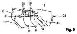
図1乃至図5に描かれた装置は、ハウジング1を備えている。ハウジング1の内部には、いくつかの電気接触要素3が表面に配置されたキャリアプレート2が配置される。これらの接触要素3の各々は信号ケーブル4に接続され、信号ケーブルは、ハウジング1の一端の開口部を通ってハウジングから延出される。信号ケーブル4は、例えば、測定装置(不図示)に繋がっており、これによって回路基板5の機能テストが実行される。機能テストを実行するため、接触要素3の各々は回路基板5の回路経路の1つと所定位置で接触するように、回路基板5は規定の方式で接触要素3と接触される。
The device depicted in FIGS. 1 to 5 includes a housing 1. Arranged inside the housing 1 is a carrier plate 2 on which several electrical contact elements 3 are arranged on the surface. Each of these contact elements 3 is connected to a
接触要素3との接触を達成するため、ハウジング1の内部に配置されるインテーク要素7により形成されるインテーク6へ回路基板5の一端部が挿入される。好ましくはプラスチックから製造される、インテーク要素7は2つの部品(特に図5を参照)、つまりインテーク6と、これに弾性接続されてハウジング1の内部で移動不能に固定される固定プレート8とを含む。インテーク6は、回路基板5の挿入セクションを五つの面(挿入端面、上面、両側面、及び下面)で少なくとも部分的に収納して、特に、接触される回路経路が配置される下面のセクションのみを露出したままにするように設計される。これにより、回路基板5は、インテーク6により形成されるインテークスロットの底面に端面が当接するほど深くインテークスロットへ挿入される。
In order to achieve contact with the contact element 3, one end of the circuit board 5 is inserted into the
装置は、スライダー9の形状の作動要素も含む。スライダー9は、ハウジング1の対応スロット内で案内される隆起部10を形成する。隆起部10を用いることにより、スライダー9は、ハウジング1のスロット内で規定の方向に手動で移動させることができる。また、隆起部10の表面の平行な凹溝は、例えばスライダーが手の親指で操作される時に、滑りに対する適切な抵抗を保証する。
The device also includes an actuating element in the form of a slider 9. The slider 9 forms a raised
スライダー9が移動されるときには、スライダー9はインテークプレート7の上面を摺動する。スライダー9の下面がインテーク要素7の固定プレート8の上面と単独に接触する図1,図2,図4に示された初期位置から始まるスライダー9の移動により、スライダー9の前端部はインテーク6の上面を摺動する。その結果、無負荷初期位置で上面が固定プレート8の上面と共面になくスライダー9の移動方向に若干上向きになっているインテーク6が、下向きに旋回する。この移動は、インテーク6と固定プレート8とのばね負荷接続による変形から生じる弾性力により抵抗される。インテーク6の旋回により、インテークは、回路基板5の挿入セクションとともに接触要素3へ移動する。
When the slider 9 is moved, the slider 9 slides on the upper surface of the intake plate 7. By moving the slider 9 starting from the initial position shown in FIGS. 1, 2, and 4 where the lower surface of the slider 9 comes into contact with the upper surface of the fixing
この移動の過程で、回路基板5は、最初に、いくつかのテーパ状の位置決めピン(不図示)が回路基板5の対応する位置決め開口部に嵌合して、接触要素3に対して正確に位置決めされる(図1参照)。位置決め開口部への位置決めピンの嵌合と、その結果生じる回路基板5の位置決めの後に、つまりインテーク6とこれに収容される回路基板5のセクションとのさらなる旋回の後に初めて、回路基板5の下面に配置される回路経路と接触要素3との接触が行われる。これは、回路経路上の想定位置で正確に接触が行われることを保証する。
In the course of this movement, the circuit board 5 initially has several tapered locating pins (not shown) fitted into the corresponding locating openings in the circuit board 5 to accurately Positioned (see FIG. 1). The bottom surface of the circuit board 5 is only after the positioning pin has been fitted into the positioning opening and the resulting positioning of the circuit board 5, i.e. after further swiveling of the
図3に示されたスライダー9の位置では、つまりインテーク6の自由端部の方向にスライダーができる限り深く押し込まれると、回路基板5はスライダーの下方に配置された接触要素3と接触する。装置のこの接触位置では、スライダー9はフォースロック方式(自動ロック)で固定されるため、スライダー9を手動にて押し戻すことにより接触が能動的に切断されなければならない。
In the position of the slider 9 shown in FIG. 3, that is, when the slider is pushed in as deeply as possible in the direction of the free end of the
スライダー9のフォースロック固定は、スライダー9の接触面と、ハウジング1又はインテーク要素7の関連する接触面との間に発生する摩擦によりもたらされる。インテーク6がばね負荷状態であることでスライダー9がインテークとハウジング1との間にクランプされるので、この摩擦は、所望のフォースロック固定が達成されるほど大きくなるように容易に選択することができる。このばね負荷状態は、インテーク6と固定プレート8との接続部の変形を生じさせるばかりでなく、接触要素3が回路基板5へ伝達する弾性力を付加的に生じさせる一方で、回路基板はこれらの弾性力をインテーク6へ伝達する。この目的のため、接触要素3は、ばね装着されるか、少なくとも2つの部品が(特に伸縮性の)スプリング要素の張力に反して、相互に対して変位することが可能なばね接触ピンの形状で設計することができる。
The force lock fixing of the slider 9 is caused by the friction generated between the contact surface of the slider 9 and the associated contact surface of the housing 1 or the intake element 7. Since the slider 9 is clamped between the intake and the housing 1 when the
HF信号が回路基板5と接触要素3とに接触することにより伝送されるのであれば、接触要素3は、例えば、従来のコプラナーLIGA接点(co-planar LIGA contacts)として設計することが可能である。他方で、直流が伝達される場合には、接点は、特に、従来のばね接触ピンであり得る。当然、異なる接触要素の組み合わせ(例えばLIGA接点とばね接触ピン)も使用することが可能である。 If the HF signal is transmitted by contacting the circuit board 5 and the contact element 3, the contact element 3 can be designed, for example, as conventional co-planar LIGA contacts. . On the other hand, if direct current is transmitted, the contacts can in particular be conventional spring contact pins. Of course, combinations of different contact elements (eg LIGA contacts and spring contact pins) can also be used.
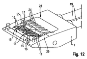
図6乃至図13に示された本発明による装置の実施形態は、2つの部品からなるハウジングを備える。ハウジングの本体11(第2ハウジング部品)は装置の下部セクションの一部である。ハウジングのカバー12(第1ハウジング部品)は装置の上部セクションの一部である。本体11とカバー12とは、2つの円筒形の位置合わせピン13を用いることにより、ロッカースイッチの方式で回転可能に、一体に接続される。
The embodiment of the device according to the invention shown in FIGS. 6 to 13 comprises a two-part housing. The housing body 11 (second housing part) is part of the lower section of the device. The housing cover 12 (first housing part) is part of the upper section of the device. The
ハウジングの本体11は、2つの(導電性)HF接触要素14が配置される嵌着凹部を形成する。HF接触要素14は、共面金属製接触要素として設計され、各々が、中央接触部15とともに、中央接触部15に並んで共面に位置合わせされた状態で側方に配置される2つの外側接触部16を含む。例えばいわゆるLIGA方法を用いることにより製造される中央接触部15及び外側接触部16は、電気絶縁空隙をその間に形成する。その相互に対する位置は、各事例において、ケーブル側端部の近傍でHF接触要素14に(接着などにより)固定される2つの絶縁体17により確保される。HF接触要素14は、各事例において、絶縁体17の1つにより、ハウジングの本体11と(接着などにより)接続される。
The
HF接触要素14の接触側端部と関連する絶縁体17との間に配置されるHF接触要素のセクションは、空間へ自由に突出する。これは、テストされる回路基板18(図8参照)の関連する接触点との接触時に、接点側端部に形成されるHF接触要素14の接触点を弾性により撓曲させる。これは、規定の接触圧力と公差補正とを保証する。
The section of the HF contact element that is arranged between the contact end of the
HF接触要素14は、ケーブル側端部で同軸ケーブル19と各々接続されている。この目的のため、端部がテーパ状である各同軸ケーブル19の内側導体20は、関連するHF接触要素14の中央接触部15と接触するのに対して、HF接触要素14の各々の2つの外側接触部16は、(導電性本体11を介して)導電状態で、関連する同軸ケーブル19の外側導体39と接触される。
The
高周波信号は、HF接触要素14と同軸ケーブル19とを介して、回路基板18と測定装置(不図示)との間で伝送される。高周波信号の良好なシールドを設けるため、ハウジングの本体11は、導電性であり、例えば金属製であるか金属被覆(例えば金属コーティング)プラスチックから設計される。共面接触要素としてのHF接触要素14の設計とともに同軸ケーブル19を用いることによる伝送は、高周波信号の良好なシールドに寄与する。
The high frequency signal is transmitted between the
本体11は、回路基板18を装置に正確に位置決めするとともに、これを装置に固定するため、回路基板18の関連する位置決め開口部22に嵌合する2つの位置決めポスト21も備える。2対の位置決めポスト/位置決め開口部の直径が異なることは、回路基板18が正確な配向で装置に嵌着されることを保証する。
The
装置の下部セクションは、スプリングコーム23の形状のスプリング要素も含む(図11参照)。これは、スプリングコーム23を介してハウジングの本体11に固定される本体を有する。複数のスプリングフィンガ24が本体から延出する。スプリングコーム23は、装置の上部セクションに形成される接触領域(DC接触要素)と回路基板18との確実な接触を保証するために設けられる。こうして2つの側方支持アーム25は、スプリングフィンガ24に負荷がかけられた時に、スプリングコーム23が上傾するのを防止する。スプリングコーム23がプラスチックで製造されると有利である。
The lower section of the device also includes a spring element in the form of a spring comb 23 (see FIG. 11). This has a body that is fixed to the
ハウジングのカバー12は、回路基板18のためのインテーク26を形成する。2つの側方ガイドスロット27は、こうして、回路基板18の挿入及び引き抜き動作を案内する。リボン導体28の一端部は、インテーク26の内部に突出する。端部接触領域(DC接触要素30)を形成する下部セクション又は挿入回路基板18と対面するリボン導体28の面に、いくつかの回路経路29が配置される。これらは、回路基板18上の回路経路31の関連する接触領域と接触するために設けられる。装置が作動しているとき、直流のみが回路経路29,31を介して伝送されると想定されるため、シールドについての費用は必要ない。そのため、ハウジングのカバー12もまた、プラスチック(熱可塑性プラスチック)で製造されても有利である。位置決め及び固定のため、リボン導体28は、カバー12の位置決めポスト32が突出する位置決め開口部を有する。加えて、介在するエラストマ要素34によりカバー12とスプリング要素33との間にクランプされることで、リボン導体28はカバー12に固定される。これらの要素とカバー12との接続は、例えば、カバー12に形成され、スプリング要素33の固定開口部に延在するリベットピン35を用いることによりもたらすことができる。リベットピン35の自由端部は、その直径が端部領域で拡大されるように、熱的に、又は圧力の付加により変形され得る。これは、スプリング要素33とのフォームロック接続を形成する。望ましくは、リベットピン35の変形は、スプリング要素33への圧力の同時付加と、その結果生じるエラストマ要素34の圧縮とにより実行され、エラストマ要素は、リベットピン35の変形後に、少なくとも部分的に組み立てられた状態にある。これは、カバー12へのリボン導体28の固定をほぼ遊びを含まないものにする。
The
例えば図6に示すように、装置が準備されると、レッグスプリングとして形成されたスプリング要素33が、ハウジング又は装置を閉位置(第1回転位置)に付勢する。この位置では、位置決めポスト21がインテーク26に向けて突出するので、回路基板18はインテーク26に挿入させることができない。
For example, as shown in FIG. 6 , when the device is prepared, a
インテーク26への回路基板18の挿入は、図7に示された装置の開位置(第2回転位置)でのみ可能である。装置を開くため、同軸ケーブル19とともにリボン導体28が出現する端部において、手動にて一緒に押圧されなければならない。こうすると、ハウジングの本体11及びカバー12が若干広がるため、位置決めポスト21がインテーク26を開く。それから、軸方向ストッパーに当たるまで回路基板18がインテーク26へ挿入されることにより、回路基板18の正確な角度位置合わせを保証するため、回路基板18の前縁部にある2つの鋭角収束切欠き37がカバー12の位置決めポスト32と相互作用を行う。位置決めポスト21と同様に、回路基板18の長手軸における切欠き37の非対称配置は、回路基板18を間違った面を上にしてインテーク26に(完全に)挿入されることを防止する。
The
回路基板18の完全挿入の後で、ハウジングへの圧力が解放される。それから、スプリング要素33がハウジングの2つの部品を閉位置へ移動させ、閉位置に保持(固定)する。こうして、下部セクションの位置決めポスト21は、回路基板18の位置決め開口部22に嵌合する。これは、回路基板18を装置に対して正確に位置決めして固定させる。同時に、HF接触要素14は、回路基板18の下面で対応するHF接触点38と接触し、HF接触要素14は、充分な接触圧力及び公差の補正を生じるため、若干弾性変形される。2つのストップピン36は、こうして回路基板18と当接して、HF接触要素14の弾性変形を制限し、HF接触要素がダメージを受けることを防止する。この目的のため、HF接触要素14は規定量だけストップピン36よりも突出する。リボン導体28のDC接触要素30は、回路基板18の上面の関連する回路経路31とも接触する(DC接点ペア)。装置を閉じることで弾性変形されるスプリングコーム23のスプリングフィンガ24は、こうして、充分な接触圧力と公差補正とを保証する。この例示的実施形態では、各DC接点ペアに1つのスプリングフィンガ24が設けられる。これは、必要な接触圧力が各DC接点ペアに付加されること、及び回路基板18が可撓性キャリアプレート38を有する際に、個々の公差補正が、各々に対して達成されることを保証することを可能にする。
After complete insertion of the
スプリングコーム23の代替物として、共通のばね本体(例えばレッグスプリングの形状)を備えたスプリング要素(不図示)を使用し、弾性材料製の個別接触タブが回路基板18と対面する縁部(連続圧接触縁部として設計)に装着されることによっても、対応する機能を達成することが可能である。この事例では、ばね本体は接触圧を実質的に保証するのに対して、接触タブは個別の公差補正を保証する。
As an alternative to the
Claims (8)
直流の伝送のための少なくとも1つのDC接触要素(30)と、
回路基板(18)の少なくとも1つのセクションが挿入されることが可能なインテーク(26)と、
前記インテーク(26)を形成する第1ハウジング部品と、前記HF接触要素(14)の少なくとも1つを収納する第2ハウジング部品とを含み、2つのハウジング部品が相互に対して移動することが可能なハウジングと、
前記HF接触要素(14)が接触されるまで前記回路基板(18)とともに前記インテーク(26)を前記HF接触要素(14)に対して移動させるための手段と、
前記HF接触要素(14)が接触する位置に前記回路基板(18)を固定するための手段と、
を含み、
2つのハウジング部品は、相互に回転することが可能であり、前記インテーク(26)へ差し込まれた回路基板(18)は第1回転位置で前記HF接触要素(14)と接触し、前記インテーク(26)へ差し込まれた前記回路基板(18)は第2回転位置で前記HF接触要素(14)と接触せず、前記2つのハウジング部品は、スプリング要素(33)を用いることにより、前記第1回転位置に付勢され、
少なくとも1つのHF接触要素(14)は、2つの外側接触部(16)の間に共面に位置合わせされた状態で配置される中央接触部(15)を含み、
前記中央接触部(15)は、内側導体(20)と電気的に接続され、
前記外側接触部(16)は、装置から延出する同軸ケーブル(19)の外側導体と電気的に接続され、
前記DC接触要素(30)は、装置から延出するリボン導体と電気的に接続されることを特徴とする、回路基板(18)を接触させるための装置。 One or more HF contact elements (14) for transmission of high-frequency signals;
At least one DC contact element (30) for direct current transmission;
An intake (26) into which at least one section of the circuit board (18) can be inserted;
Including a first housing part forming the intake (26) and a second housing part containing at least one of the HF contact elements (14), the two housing parts being movable relative to one another A housing,
Means for moving the intake (26) with the circuit board (18) relative to the HF contact element (14) until the HF contact element (14) is contacted;
Means for securing the circuit board (18) in a position where the HF contact element (14) contacts;
Including
The two housing parts can rotate relative to each other, and the circuit board (18) inserted into the intake (26) contacts the HF contact element (14) in a first rotational position, and the intake ( 26) the circuit board (18) inserted into the second rotation position does not contact with the HF contact element (14), and the two housing parts use the spring element (33) to make the first Biased to the rotational position ,
The at least one HF contact element (14) includes a central contact (15) disposed in coplanar alignment between the two outer contacts (16);
The central contact (15) is electrically connected to the inner conductor (20);
The outer contact (16) is electrically connected to the outer conductor of a coaxial cable (19) extending from the device;
Device for contacting a circuit board (18), characterized in that the DC contact element (30) is electrically connected to a ribbon conductor extending from the device.
前記回路基板(18)は、移動時に、前記HF接触要素(14)と接触する前にセンタリングされることを特徴とする装置。 The apparatus of claim 1.
The device characterized in that the circuit board (18) is centered prior to contacting the HF contact element (14) during movement.
前記回路基板(18)の開口部に押圧されるセンタリングピン(21)を有することを特徴とする装置。 The apparatus of claim 2.
A device comprising a centering pin (21) pressed against the opening of the circuit board (18).
形状及び/又は寸法が異なる、少なくとも2つのセンタリングピン(21)を有することを特徴とする装置。 The apparatus of claim 3.
Device having at least two centering pins (21) of different shape and / or dimensions.
前記インテーク(26)は、ばね装着されていることを特徴とする装置。 The apparatus according to any one of claims 1 to 4,
The device (26) characterized in that the intake (26) is spring mounted.
前記回路基板(18)が前記第1回転位置で前記インテーク(26)へ差し込まれることを防止する手段を有することを特徴とする装置。 The device according to any one of claims 1 to 5,
An apparatus comprising means for preventing the circuit board (18) from being inserted into the intake (26) in the first rotational position.
前記センタリングピン(21)は、前記回路基板(18)が前記第1回転位置で前記インテーク(26)へ差し込まれることを防止することを特徴とする装置。 The apparatus of claim 3.
The centering pin (21) prevents the circuit board (18) from being inserted into the intake (26) at the first rotational position.
Applications Claiming Priority (3)
| Application Number | Priority Date | Filing Date | Title |
|---|---|---|---|
| DE202012001645.8 | 2012-02-17 | ||
| DE202012001645U DE202012001645U1 (en) | 2012-02-17 | 2012-02-17 | Device for contacting a printed circuit board |
| PCT/EP2013/000214 WO2013120580A1 (en) | 2012-02-17 | 2013-01-24 | Device for contacting a circuit board |
Publications (3)
| Publication Number | Publication Date |
|---|---|
| JP2015507341A JP2015507341A (en) | 2015-03-05 |
| JP2015507341A5 JP2015507341A5 (en) | 2016-02-18 |
| JP6254537B2 true JP6254537B2 (en) | 2017-12-27 |
Family
ID=47632970
Family Applications (1)
| Application Number | Title | Priority Date | Filing Date |
|---|---|---|---|
| JP2014556943A Active JP6254537B2 (en) | 2012-02-17 | 2013-01-24 | Device for contacting circuit boards |
Country Status (10)
| Country | Link |
|---|---|
| US (1) | US9240643B2 (en) |
| EP (1) | EP2815462B1 (en) |
| JP (1) | JP6254537B2 (en) |
| KR (1) | KR101901743B1 (en) |
| CN (1) | CN104115336B (en) |
| CA (1) | CA2876631C (en) |
| DE (1) | DE202012001645U1 (en) |
| HK (1) | HK1201993A1 (en) |
| TW (1) | TWM462374U (en) |
| WO (1) | WO2013120580A1 (en) |
Families Citing this family (7)
| Publication number | Priority date | Publication date | Assignee | Title |
|---|---|---|---|---|
| US9568499B2 (en) * | 2013-11-22 | 2017-02-14 | Tektronix, Inc. | High performance LIGA spring interconnect system for probing application |
| US9142903B2 (en) | 2013-11-22 | 2015-09-22 | Tektronix, Inc. | High performance multiport connector system using LIGA springs |
| CN104319505B (en) * | 2014-11-17 | 2018-01-19 | 合肥京东方光电科技有限公司 | Flexible printed circuit board grafting tool |
| JP6821918B2 (en) * | 2016-02-18 | 2021-01-27 | 大日本印刷株式会社 | Light guide plate and display device |
| US10847912B2 (en) | 2018-03-19 | 2020-11-24 | Rohde & Schwarz Gmbh & Co. Kg | Broadband socket connector, broadband plug connector, and system thereof |
| TWI718610B (en) * | 2018-08-09 | 2021-02-11 | 日商歐姆龍股份有限公司 | Probe unit |
| CN114778902B (en) * | 2022-06-27 | 2022-11-11 | 武汉永鼎光通科技有限公司 | PCBA adds electric testing arrangement and prevents crossing anchor clamps of inserting |
Family Cites Families (19)
| Publication number | Priority date | Publication date | Assignee | Title |
|---|---|---|---|---|
| FR1174063A (en) | 1957-03-30 | 1959-03-05 | Electrical terminal couplers | |
| FR2492213A1 (en) * | 1980-10-15 | 1982-04-16 | Labo Electronique Physique | Reader for plastic transaction or data cards with tilt locking - uses sleeve into which card is inserted and electromagnet to allow sleeve to tip so card is trapped and positioned against reader |
| JPS5972753U (en) * | 1982-11-04 | 1984-05-17 | 株式会社東芝 | Attached equipment |
| JPS59187162U (en) * | 1983-05-30 | 1984-12-12 | 三菱電機株式会社 | printed wiring board equipment |
| JPS6022795A (en) * | 1983-07-18 | 1985-02-05 | Tokyo Tatsuno Co Ltd | Reading and writing device of plate-shaped memory medium |
| US4602351A (en) * | 1983-07-06 | 1986-07-22 | Tokyo Tatsuno Co., Ltd. | Device for reading and writing IC-external storage cards |
| US4700997A (en) * | 1986-11-14 | 1987-10-20 | Minnesota Mining And Manufacturing Company | Electrical connector |
| GB2235078B (en) * | 1989-08-19 | 1993-09-08 | Technophone Ltd | Card reader |
| US6447305B1 (en) * | 1996-05-14 | 2002-09-10 | Miraco, Inc. | Circuit to printed circuit board stored energy connector |
| JP2000277218A (en) * | 1999-03-19 | 2000-10-06 | Ace Five:Kk | Cable assembly |
| US6447317B1 (en) * | 2001-07-11 | 2002-09-10 | Hon Hai Precision Ind. Co., Ltd. | Backplane connector |
| US6623312B2 (en) * | 2001-10-04 | 2003-09-23 | Unilead International | Precordial electrocardiogram electrode connector |
| JP3976276B2 (en) * | 2005-06-10 | 2007-09-12 | 日本航空電子工業株式会社 | Inspection device |
| JP4558588B2 (en) * | 2005-06-14 | 2010-10-06 | 第一電子工業株式会社 | connector |
| JP2008135209A (en) * | 2006-11-27 | 2008-06-12 | Fujifilm Corp | Clip-type connector |
| JP4908374B2 (en) * | 2007-10-17 | 2012-04-04 | 日本航空電子工業株式会社 | Connector device |
| JP5436088B2 (en) * | 2008-08-19 | 2014-03-05 | 矢崎総業株式会社 | Flexible aggregation wiring connector |
| US20100105230A1 (en) * | 2008-10-23 | 2010-04-29 | Sony Ericsson Mobile Communications Ab | Connector |
| JP5410872B2 (en) * | 2009-07-27 | 2014-02-05 | モレックス インコーポレイテド | Hybrid connector |
-
2012
- 2012-02-17 DE DE202012001645U patent/DE202012001645U1/en not_active Expired - Lifetime
-
2013
- 2013-01-24 KR KR1020147026013A patent/KR101901743B1/en active IP Right Grant
- 2013-01-24 EP EP13702340.4A patent/EP2815462B1/en active Active
- 2013-01-24 CN CN201380009752.8A patent/CN104115336B/en active Active
- 2013-01-24 JP JP2014556943A patent/JP6254537B2/en active Active
- 2013-01-24 CA CA2876631A patent/CA2876631C/en active Active
- 2013-01-24 US US14/379,033 patent/US9240643B2/en active Active
- 2013-01-24 WO PCT/EP2013/000214 patent/WO2013120580A1/en active Application Filing
- 2013-02-18 TW TW102203123U patent/TWM462374U/en not_active IP Right Cessation
-
2015
- 2015-03-10 HK HK15102439.8A patent/HK1201993A1/en not_active IP Right Cessation
Also Published As
| Publication number | Publication date |
|---|---|
| US20150024619A1 (en) | 2015-01-22 |
| CA2876631C (en) | 2018-04-10 |
| JP2015507341A (en) | 2015-03-05 |
| CN104115336B (en) | 2017-02-22 |
| CA2876631A1 (en) | 2013-08-22 |
| DE202012001645U1 (en) | 2013-05-21 |
| EP2815462A1 (en) | 2014-12-24 |
| KR101901743B1 (en) | 2018-09-28 |
| EP2815462B1 (en) | 2018-08-08 |
| CN104115336A (en) | 2014-10-22 |
| US9240643B2 (en) | 2016-01-19 |
| HK1201993A1 (en) | 2015-09-11 |
| WO2013120580A1 (en) | 2013-08-22 |
| KR20140125442A (en) | 2014-10-28 |
| TWM462374U (en) | 2013-09-21 |
Similar Documents
| Publication | Publication Date | Title |
|---|---|---|
| JP6254537B2 (en) | Device for contacting circuit boards | |
| US10490955B2 (en) | Poke-in electrical connector | |
| KR101235936B1 (en) | Coaxial connector | |
| US6848928B2 (en) | Socket | |
| US20060094277A1 (en) | Card edge connector with latching arms | |
| JPH10144439A (en) | Ic socket for bga package | |
| US9570830B2 (en) | Terminal holding member and clamping device including terminal holding member and electroconductive member | |
| CN102326303B (en) | Coaxial connector | |
| JP3177493U (en) | Test clip for 4-terminal measurement | |
| CN110890642B (en) | Rotary open type clamping component and connecting device with same | |
| JP5693720B2 (en) | Plug-in connector including an insulation displacement terminal and an insulation body to be moored | |
| EP2573884B1 (en) | Socket for electric component | |
| KR101830415B1 (en) | Connector | |
| KR101786594B1 (en) | Connector | |
| US9196987B2 (en) | Connector | |
| US9500674B2 (en) | Probe structure | |
| JP2001043940A (en) | Electric connector | |
| JP7397314B2 (en) | inspection socket | |
| KR20090004122U (en) | Lever type connector | |
| US10847934B2 (en) | Electrical connectors for flat circuits | |
| TWI589070B (en) | Electrical connector | |
| JP4117827B2 (en) | Socket for electrical parts | |
| CN114520421A (en) | Connector with a locking member | |
| TW202130061A (en) | Connector and method of manufacturing connector | |
| JP2007502521A (en) | Spring-loaded electrical terminal |
Legal Events
| Date | Code | Title | Description |
|---|---|---|---|
| A529 | Written submission of copy of amendment under article 34 pct |
Free format text: JAPANESE INTERMEDIATE CODE: A529 Effective date: 20140902 |
|
| A521 | Request for written amendment filed |
Free format text: JAPANESE INTERMEDIATE CODE: A523 Effective date: 20151222 |
|
| A621 | Written request for application examination |
Free format text: JAPANESE INTERMEDIATE CODE: A621 Effective date: 20151222 |
|
| A977 | Report on retrieval |
Free format text: JAPANESE INTERMEDIATE CODE: A971007 Effective date: 20161115 |
|
| A131 | Notification of reasons for refusal |
Free format text: JAPANESE INTERMEDIATE CODE: A131 Effective date: 20161122 |
|
| A521 | Request for written amendment filed |
Free format text: JAPANESE INTERMEDIATE CODE: A523 Effective date: 20170217 |
|
| A02 | Decision of refusal |
Free format text: JAPANESE INTERMEDIATE CODE: A02 Effective date: 20170523 |
|
| A521 | Request for written amendment filed |
Free format text: JAPANESE INTERMEDIATE CODE: A523 Effective date: 20170912 |
|
| A911 | Transfer to examiner for re-examination before appeal (zenchi) |
Free format text: JAPANESE INTERMEDIATE CODE: A911 Effective date: 20171019 |
|
| TRDD | Decision of grant or rejection written | ||
| A01 | Written decision to grant a patent or to grant a registration (utility model) |
Free format text: JAPANESE INTERMEDIATE CODE: A01 Effective date: 20171114 |
|
| A61 | First payment of annual fees (during grant procedure) |
Free format text: JAPANESE INTERMEDIATE CODE: A61 Effective date: 20171130 |
|
| R150 | Certificate of patent or registration of utility model |
Ref document number: 6254537 Country of ref document: JP Free format text: JAPANESE INTERMEDIATE CODE: R150 |
|
| R250 | Receipt of annual fees |
Free format text: JAPANESE INTERMEDIATE CODE: R250 |
|
| R250 | Receipt of annual fees |
Free format text: JAPANESE INTERMEDIATE CODE: R250 |
|
| R250 | Receipt of annual fees |
Free format text: JAPANESE INTERMEDIATE CODE: R250 |
|
| R250 | Receipt of annual fees |
Free format text: JAPANESE INTERMEDIATE CODE: R250 |