EP2815439B1 - LED module with highly reflective support and method of manufacturing LED module with highly reflective support - Google Patents
LED module with highly reflective support and method of manufacturing LED module with highly reflective support Download PDFInfo
- Publication number
- EP2815439B1 EP2815439B1 EP13705413.6A EP13705413A EP2815439B1 EP 2815439 B1 EP2815439 B1 EP 2815439B1 EP 13705413 A EP13705413 A EP 13705413A EP 2815439 B1 EP2815439 B1 EP 2815439B1
- Authority
- EP
- European Patent Office
- Prior art keywords
- layer
- dam
- led
- metallic layer
- lacquer
- Prior art date
- Legal status (The legal status is an assumption and is not a legal conclusion. Google has not performed a legal analysis and makes no representation as to the accuracy of the status listed.)
- Active
Links
- 238000004519 manufacturing process Methods 0.000 title claims description 10
- 239000010410 layer Substances 0.000 claims description 260
- 239000004922 lacquer Substances 0.000 claims description 102
- 239000000853 adhesive Substances 0.000 claims description 30
- 230000001070 adhesive effect Effects 0.000 claims description 30
- 239000000919 ceramic Substances 0.000 claims description 25
- 238000000034 method Methods 0.000 claims description 23
- 229910052751 metal Inorganic materials 0.000 claims description 22
- 239000002184 metal Substances 0.000 claims description 22
- BQCADISMDOOEFD-UHFFFAOYSA-N Silver Chemical compound [Ag] BQCADISMDOOEFD-UHFFFAOYSA-N 0.000 claims description 19
- 229910052709 silver Inorganic materials 0.000 claims description 19
- 239000004332 silver Substances 0.000 claims description 19
- 229910052782 aluminium Inorganic materials 0.000 claims description 12
- XAGFODPZIPBFFR-UHFFFAOYSA-N aluminium Chemical compound [Al] XAGFODPZIPBFFR-UHFFFAOYSA-N 0.000 claims description 12
- 230000008859 change Effects 0.000 claims description 7
- 239000012044 organic layer Substances 0.000 claims description 5
- 238000001816 cooling Methods 0.000 claims 1
- 239000000463 material Substances 0.000 description 49
- 229920000642 polymer Polymers 0.000 description 30
- 239000000758 substrate Substances 0.000 description 27
- 239000007788 liquid Substances 0.000 description 23
- 229920005989 resin Polymers 0.000 description 20
- 239000011347 resin Substances 0.000 description 20
- 239000002245 particle Substances 0.000 description 19
- VYPSYNLAJGMNEJ-UHFFFAOYSA-N Silicium dioxide Chemical compound O=[Si]=O VYPSYNLAJGMNEJ-UHFFFAOYSA-N 0.000 description 13
- PCHJSUWPFVWCPO-UHFFFAOYSA-N gold Chemical compound [Au] PCHJSUWPFVWCPO-UHFFFAOYSA-N 0.000 description 10
- 229910052737 gold Inorganic materials 0.000 description 10
- 239000010931 gold Substances 0.000 description 10
- 238000006243 chemical reaction Methods 0.000 description 9
- 238000000576 coating method Methods 0.000 description 9
- 229920002959 polymer blend Polymers 0.000 description 9
- 230000008569 process Effects 0.000 description 9
- 238000005516 engineering process Methods 0.000 description 8
- 239000000945 filler Substances 0.000 description 8
- 229920001296 polysiloxane Polymers 0.000 description 8
- PXHVJJICTQNCMI-UHFFFAOYSA-N Nickel Chemical compound [Ni] PXHVJJICTQNCMI-UHFFFAOYSA-N 0.000 description 7
- 239000011248 coating agent Substances 0.000 description 7
- 239000011159 matrix material Substances 0.000 description 6
- 239000000049 pigment Substances 0.000 description 6
- 239000000377 silicon dioxide Substances 0.000 description 6
- 235000012239 silicon dioxide Nutrition 0.000 description 6
- OAICVXFJPJFONN-UHFFFAOYSA-N Phosphorus Chemical compound [P] OAICVXFJPJFONN-UHFFFAOYSA-N 0.000 description 5
- 229910010413 TiO 2 Inorganic materials 0.000 description 5
- GWEVSGVZZGPLCZ-UHFFFAOYSA-N Titan oxide Chemical compound O=[Ti]=O GWEVSGVZZGPLCZ-UHFFFAOYSA-N 0.000 description 5
- 230000008901 benefit Effects 0.000 description 5
- 238000007650 screen-printing Methods 0.000 description 5
- KDLHZDBZIXYQEI-UHFFFAOYSA-N Palladium Chemical compound [Pd] KDLHZDBZIXYQEI-UHFFFAOYSA-N 0.000 description 4
- 229910004283 SiO 4 Inorganic materials 0.000 description 4
- 239000013307 optical fiber Substances 0.000 description 4
- 239000011236 particulate material Substances 0.000 description 4
- 239000004033 plastic Substances 0.000 description 4
- 239000000126 substance Substances 0.000 description 4
- 229910004298 SiO 2 Inorganic materials 0.000 description 3
- MCMNRKCIXSYSNV-UHFFFAOYSA-N Zirconium dioxide Chemical compound O=[Zr]=O MCMNRKCIXSYSNV-UHFFFAOYSA-N 0.000 description 3
- 229910052788 barium Inorganic materials 0.000 description 3
- 239000010949 copper Substances 0.000 description 3
- 229910052736 halogen Inorganic materials 0.000 description 3
- 150000002367 halogens Chemical class 0.000 description 3
- 229910052759 nickel Inorganic materials 0.000 description 3
- 230000003287 optical effect Effects 0.000 description 3
- 239000003973 paint Substances 0.000 description 3
- 238000007639 printing Methods 0.000 description 3
- RYGMFSIKBFXOCR-UHFFFAOYSA-N Copper Chemical compound [Cu] RYGMFSIKBFXOCR-UHFFFAOYSA-N 0.000 description 2
- RTZKZFJDLAIYFH-UHFFFAOYSA-N Diethyl ether Chemical compound CCOCC RTZKZFJDLAIYFH-UHFFFAOYSA-N 0.000 description 2
- 241000907903 Shorea Species 0.000 description 2
- 238000000149 argon plasma sintering Methods 0.000 description 2
- 229910002113 barium titanate Inorganic materials 0.000 description 2
- 239000012876 carrier material Substances 0.000 description 2
- 229910052681 coesite Inorganic materials 0.000 description 2
- 239000004020 conductor Substances 0.000 description 2
- 238000010276 construction Methods 0.000 description 2
- 229910052802 copper Inorganic materials 0.000 description 2
- 229910052906 cristobalite Inorganic materials 0.000 description 2
- 238000009826 distribution Methods 0.000 description 2
- 230000000694 effects Effects 0.000 description 2
- 229910021485 fumed silica Inorganic materials 0.000 description 2
- 239000011521 glass Substances 0.000 description 2
- 238000007654 immersion Methods 0.000 description 2
- 239000003049 inorganic solvent Substances 0.000 description 2
- 229910001867 inorganic solvent Inorganic materials 0.000 description 2
- 239000000203 mixture Substances 0.000 description 2
- 230000005693 optoelectronics Effects 0.000 description 2
- 230000003647 oxidation Effects 0.000 description 2
- 238000007254 oxidation reaction Methods 0.000 description 2
- 230000001590 oxidative effect Effects 0.000 description 2
- TWNQGVIAIRXVLR-UHFFFAOYSA-N oxo(oxoalumanyloxy)alumane Chemical compound O=[Al]O[Al]=O TWNQGVIAIRXVLR-UHFFFAOYSA-N 0.000 description 2
- 229910052763 palladium Inorganic materials 0.000 description 2
- 239000002861 polymer material Substances 0.000 description 2
- 239000011253 protective coating Substances 0.000 description 2
- 239000011241 protective layer Substances 0.000 description 2
- 239000000243 solution Substances 0.000 description 2
- 229910052682 stishovite Inorganic materials 0.000 description 2
- 239000010936 titanium Substances 0.000 description 2
- 229910052905 tridymite Inorganic materials 0.000 description 2
- 229910018072 Al 2 O 3 Inorganic materials 0.000 description 1
- 102100032047 Alsin Human genes 0.000 description 1
- 101710187109 Alsin Proteins 0.000 description 1
- 239000004593 Epoxy Substances 0.000 description 1
- ZLMJMSJWJFRBEC-UHFFFAOYSA-N Potassium Chemical compound [K] ZLMJMSJWJFRBEC-UHFFFAOYSA-N 0.000 description 1
- 229910003564 SiAlON Inorganic materials 0.000 description 1
- 238000010521 absorption reaction Methods 0.000 description 1
- 239000000654 additive Substances 0.000 description 1
- JRPBQTZRNDNNOP-UHFFFAOYSA-N barium titanate Chemical compound [Ba+2].[Ba+2].[O-][Ti]([O-])([O-])[O-] JRPBQTZRNDNNOP-UHFFFAOYSA-N 0.000 description 1
- 229920005601 base polymer Polymers 0.000 description 1
- 230000005540 biological transmission Effects 0.000 description 1
- 238000004132 cross linking Methods 0.000 description 1
- 230000001419 dependent effect Effects 0.000 description 1
- 238000001514 detection method Methods 0.000 description 1
- KPUWHANPEXNPJT-UHFFFAOYSA-N disiloxane Chemical class [SiH3]O[SiH3] KPUWHANPEXNPJT-UHFFFAOYSA-N 0.000 description 1
- 239000006185 dispersion Substances 0.000 description 1
- 239000003365 glass fiber Substances 0.000 description 1
- 239000003292 glue Substances 0.000 description 1
- 239000008187 granular material Substances 0.000 description 1
- 230000017525 heat dissipation Effects 0.000 description 1
- 125000002887 hydroxy group Chemical group [H]O* 0.000 description 1
- 238000002347 injection Methods 0.000 description 1
- 239000007924 injection Substances 0.000 description 1
- 238000002955 isolation Methods 0.000 description 1
- 230000007246 mechanism Effects 0.000 description 1
- 125000002496 methyl group Chemical group [H]C([H])([H])* 0.000 description 1
- 238000003801 milling Methods 0.000 description 1
- 230000004048 modification Effects 0.000 description 1
- 238000012986 modification Methods 0.000 description 1
- 229910052605 nesosilicate Inorganic materials 0.000 description 1
- 150000004767 nitrides Chemical class 0.000 description 1
- 239000003960 organic solvent Substances 0.000 description 1
- 150000004762 orthosilicates Chemical class 0.000 description 1
- RVTZCBVAJQQJTK-UHFFFAOYSA-N oxygen(2-);zirconium(4+) Chemical compound [O-2].[O-2].[Zr+4] RVTZCBVAJQQJTK-UHFFFAOYSA-N 0.000 description 1
- 238000006116 polymerization reaction Methods 0.000 description 1
- 229910052700 potassium Inorganic materials 0.000 description 1
- 239000011591 potassium Substances 0.000 description 1
- 230000001681 protective effect Effects 0.000 description 1
- 230000005855 radiation Effects 0.000 description 1
- 238000002310 reflectometry Methods 0.000 description 1
- 230000000717 retained effect Effects 0.000 description 1
- 229910000679 solder Inorganic materials 0.000 description 1
- 238000005476 soldering Methods 0.000 description 1
- 238000001228 spectrum Methods 0.000 description 1
- 229920001187 thermosetting polymer Polymers 0.000 description 1
- 239000004634 thermosetting polymer Substances 0.000 description 1
- QHGNHLZPVBIIPX-UHFFFAOYSA-N tin(II) oxide Inorganic materials [Sn]=O QHGNHLZPVBIIPX-UHFFFAOYSA-N 0.000 description 1
- 239000004408 titanium dioxide Substances 0.000 description 1
- OGIDPMRJRNCKJF-UHFFFAOYSA-N titanium oxide Inorganic materials [Ti]=O OGIDPMRJRNCKJF-UHFFFAOYSA-N 0.000 description 1
- XLYOFNOQVPJJNP-UHFFFAOYSA-N water Substances O XLYOFNOQVPJJNP-UHFFFAOYSA-N 0.000 description 1
Images


Classifications
-
- H—ELECTRICITY
- H01—ELECTRIC ELEMENTS
- H01L—SEMICONDUCTOR DEVICES NOT COVERED BY CLASS H10
- H01L33/00—Semiconductor devices with at least one potential-jump barrier or surface barrier specially adapted for light emission; Processes or apparatus specially adapted for the manufacture or treatment thereof or of parts thereof; Details thereof
- H01L33/48—Semiconductor devices with at least one potential-jump barrier or surface barrier specially adapted for light emission; Processes or apparatus specially adapted for the manufacture or treatment thereof or of parts thereof; Details thereof characterised by the semiconductor body packages
-
- H—ELECTRICITY
- H01—ELECTRIC ELEMENTS
- H01L—SEMICONDUCTOR DEVICES NOT COVERED BY CLASS H10
- H01L25/00—Assemblies consisting of a plurality of individual semiconductor or other solid state devices ; Multistep manufacturing processes thereof
- H01L25/03—Assemblies consisting of a plurality of individual semiconductor or other solid state devices ; Multistep manufacturing processes thereof all the devices being of a type provided for in the same subgroup of groups H01L27/00 - H01L33/00, or in a single subclass of H10K, H10N, e.g. assemblies of rectifier diodes
- H01L25/04—Assemblies consisting of a plurality of individual semiconductor or other solid state devices ; Multistep manufacturing processes thereof all the devices being of a type provided for in the same subgroup of groups H01L27/00 - H01L33/00, or in a single subclass of H10K, H10N, e.g. assemblies of rectifier diodes the devices not having separate containers
- H01L25/075—Assemblies consisting of a plurality of individual semiconductor or other solid state devices ; Multistep manufacturing processes thereof all the devices being of a type provided for in the same subgroup of groups H01L27/00 - H01L33/00, or in a single subclass of H10K, H10N, e.g. assemblies of rectifier diodes the devices not having separate containers the devices being of a type provided for in group H01L33/00
- H01L25/0753—Assemblies consisting of a plurality of individual semiconductor or other solid state devices ; Multistep manufacturing processes thereof all the devices being of a type provided for in the same subgroup of groups H01L27/00 - H01L33/00, or in a single subclass of H10K, H10N, e.g. assemblies of rectifier diodes the devices not having separate containers the devices being of a type provided for in group H01L33/00 the devices being arranged next to each other
-
- H—ELECTRICITY
- H01—ELECTRIC ELEMENTS
- H01L—SEMICONDUCTOR DEVICES NOT COVERED BY CLASS H10
- H01L25/00—Assemblies consisting of a plurality of individual semiconductor or other solid state devices ; Multistep manufacturing processes thereof
- H01L25/03—Assemblies consisting of a plurality of individual semiconductor or other solid state devices ; Multistep manufacturing processes thereof all the devices being of a type provided for in the same subgroup of groups H01L27/00 - H01L33/00, or in a single subclass of H10K, H10N, e.g. assemblies of rectifier diodes
- H01L25/10—Assemblies consisting of a plurality of individual semiconductor or other solid state devices ; Multistep manufacturing processes thereof all the devices being of a type provided for in the same subgroup of groups H01L27/00 - H01L33/00, or in a single subclass of H10K, H10N, e.g. assemblies of rectifier diodes the devices having separate containers
- H01L25/13—Assemblies consisting of a plurality of individual semiconductor or other solid state devices ; Multistep manufacturing processes thereof all the devices being of a type provided for in the same subgroup of groups H01L27/00 - H01L33/00, or in a single subclass of H10K, H10N, e.g. assemblies of rectifier diodes the devices having separate containers the devices being of a type provided for in group H01L33/00
-
- H—ELECTRICITY
- H01—ELECTRIC ELEMENTS
- H01L—SEMICONDUCTOR DEVICES NOT COVERED BY CLASS H10
- H01L33/00—Semiconductor devices with at least one potential-jump barrier or surface barrier specially adapted for light emission; Processes or apparatus specially adapted for the manufacture or treatment thereof or of parts thereof; Details thereof
- H01L33/48—Semiconductor devices with at least one potential-jump barrier or surface barrier specially adapted for light emission; Processes or apparatus specially adapted for the manufacture or treatment thereof or of parts thereof; Details thereof characterised by the semiconductor body packages
- H01L33/52—Encapsulations
-
- H—ELECTRICITY
- H01—ELECTRIC ELEMENTS
- H01L—SEMICONDUCTOR DEVICES NOT COVERED BY CLASS H10
- H01L33/00—Semiconductor devices with at least one potential-jump barrier or surface barrier specially adapted for light emission; Processes or apparatus specially adapted for the manufacture or treatment thereof or of parts thereof; Details thereof
- H01L33/48—Semiconductor devices with at least one potential-jump barrier or surface barrier specially adapted for light emission; Processes or apparatus specially adapted for the manufacture or treatment thereof or of parts thereof; Details thereof characterised by the semiconductor body packages
- H01L33/58—Optical field-shaping elements
- H01L33/60—Reflective elements
-
- H—ELECTRICITY
- H01—ELECTRIC ELEMENTS
- H01L—SEMICONDUCTOR DEVICES NOT COVERED BY CLASS H10
- H01L33/00—Semiconductor devices with at least one potential-jump barrier or surface barrier specially adapted for light emission; Processes or apparatus specially adapted for the manufacture or treatment thereof or of parts thereof; Details thereof
- H01L33/48—Semiconductor devices with at least one potential-jump barrier or surface barrier specially adapted for light emission; Processes or apparatus specially adapted for the manufacture or treatment thereof or of parts thereof; Details thereof characterised by the semiconductor body packages
- H01L33/62—Arrangements for conducting electric current to or from the semiconductor body, e.g. lead-frames, wire-bonds or solder balls
-
- H—ELECTRICITY
- H01—ELECTRIC ELEMENTS
- H01L—SEMICONDUCTOR DEVICES NOT COVERED BY CLASS H10
- H01L33/00—Semiconductor devices with at least one potential-jump barrier or surface barrier specially adapted for light emission; Processes or apparatus specially adapted for the manufacture or treatment thereof or of parts thereof; Details thereof
- H01L33/48—Semiconductor devices with at least one potential-jump barrier or surface barrier specially adapted for light emission; Processes or apparatus specially adapted for the manufacture or treatment thereof or of parts thereof; Details thereof characterised by the semiconductor body packages
- H01L33/64—Heat extraction or cooling elements
-
- H—ELECTRICITY
- H05—ELECTRIC TECHNIQUES NOT OTHERWISE PROVIDED FOR
- H05B—ELECTRIC HEATING; ELECTRIC LIGHT SOURCES NOT OTHERWISE PROVIDED FOR; CIRCUIT ARRANGEMENTS FOR ELECTRIC LIGHT SOURCES, IN GENERAL
- H05B33/00—Electroluminescent light sources
- H05B33/12—Light sources with substantially two-dimensional radiating surfaces
- H05B33/22—Light sources with substantially two-dimensional radiating surfaces characterised by the chemical or physical composition or the arrangement of auxiliary dielectric or reflective layers
-
- H—ELECTRICITY
- H05—ELECTRIC TECHNIQUES NOT OTHERWISE PROVIDED FOR
- H05K—PRINTED CIRCUITS; CASINGS OR CONSTRUCTIONAL DETAILS OF ELECTRIC APPARATUS; MANUFACTURE OF ASSEMBLAGES OF ELECTRICAL COMPONENTS
- H05K1/00—Printed circuits
- H05K1/02—Details
- H05K1/0274—Optical details, e.g. printed circuits comprising integral optical means
-
- H—ELECTRICITY
- H01—ELECTRIC ELEMENTS
- H01L—SEMICONDUCTOR DEVICES NOT COVERED BY CLASS H10
- H01L2224/00—Indexing scheme for arrangements for connecting or disconnecting semiconductor or solid-state bodies and methods related thereto as covered by H01L24/00
- H01L2224/01—Means for bonding being attached to, or being formed on, the surface to be connected, e.g. chip-to-package, die-attach, "first-level" interconnects; Manufacturing methods related thereto
- H01L2224/42—Wire connectors; Manufacturing methods related thereto
- H01L2224/47—Structure, shape, material or disposition of the wire connectors after the connecting process
- H01L2224/48—Structure, shape, material or disposition of the wire connectors after the connecting process of an individual wire connector
- H01L2224/4805—Shape
- H01L2224/4809—Loop shape
- H01L2224/48091—Arched
-
- H—ELECTRICITY
- H01—ELECTRIC ELEMENTS
- H01L—SEMICONDUCTOR DEVICES NOT COVERED BY CLASS H10
- H01L2224/00—Indexing scheme for arrangements for connecting or disconnecting semiconductor or solid-state bodies and methods related thereto as covered by H01L24/00
- H01L2224/01—Means for bonding being attached to, or being formed on, the surface to be connected, e.g. chip-to-package, die-attach, "first-level" interconnects; Manufacturing methods related thereto
- H01L2224/42—Wire connectors; Manufacturing methods related thereto
- H01L2224/47—Structure, shape, material or disposition of the wire connectors after the connecting process
- H01L2224/48—Structure, shape, material or disposition of the wire connectors after the connecting process of an individual wire connector
- H01L2224/481—Disposition
- H01L2224/48135—Connecting between different semiconductor or solid-state bodies, i.e. chip-to-chip
- H01L2224/48137—Connecting between different semiconductor or solid-state bodies, i.e. chip-to-chip the bodies being arranged next to each other, e.g. on a common substrate
-
- H—ELECTRICITY
- H01—ELECTRIC ELEMENTS
- H01L—SEMICONDUCTOR DEVICES NOT COVERED BY CLASS H10
- H01L2224/00—Indexing scheme for arrangements for connecting or disconnecting semiconductor or solid-state bodies and methods related thereto as covered by H01L24/00
- H01L2224/01—Means for bonding being attached to, or being formed on, the surface to be connected, e.g. chip-to-package, die-attach, "first-level" interconnects; Manufacturing methods related thereto
- H01L2224/42—Wire connectors; Manufacturing methods related thereto
- H01L2224/47—Structure, shape, material or disposition of the wire connectors after the connecting process
- H01L2224/48—Structure, shape, material or disposition of the wire connectors after the connecting process of an individual wire connector
- H01L2224/481—Disposition
- H01L2224/48151—Connecting between a semiconductor or solid-state body and an item not being a semiconductor or solid-state body, e.g. chip-to-substrate, chip-to-passive
- H01L2224/48221—Connecting between a semiconductor or solid-state body and an item not being a semiconductor or solid-state body, e.g. chip-to-substrate, chip-to-passive the body and the item being stacked
- H01L2224/48225—Connecting between a semiconductor or solid-state body and an item not being a semiconductor or solid-state body, e.g. chip-to-substrate, chip-to-passive the body and the item being stacked the item being non-metallic, e.g. insulating substrate with or without metallisation
- H01L2224/48227—Connecting between a semiconductor or solid-state body and an item not being a semiconductor or solid-state body, e.g. chip-to-substrate, chip-to-passive the body and the item being stacked the item being non-metallic, e.g. insulating substrate with or without metallisation connecting the wire to a bond pad of the item
-
- H—ELECTRICITY
- H01—ELECTRIC ELEMENTS
- H01L—SEMICONDUCTOR DEVICES NOT COVERED BY CLASS H10
- H01L24/00—Arrangements for connecting or disconnecting semiconductor or solid-state bodies; Methods or apparatus related thereto
- H01L24/01—Means for bonding being attached to, or being formed on, the surface to be connected, e.g. chip-to-package, die-attach, "first-level" interconnects; Manufacturing methods related thereto
- H01L24/42—Wire connectors; Manufacturing methods related thereto
- H01L24/47—Structure, shape, material or disposition of the wire connectors after the connecting process
- H01L24/48—Structure, shape, material or disposition of the wire connectors after the connecting process of an individual wire connector
-
- H—ELECTRICITY
- H01—ELECTRIC ELEMENTS
- H01L—SEMICONDUCTOR DEVICES NOT COVERED BY CLASS H10
- H01L2924/00—Indexing scheme for arrangements or methods for connecting or disconnecting semiconductor or solid-state bodies as covered by H01L24/00
- H01L2924/0001—Technical content checked by a classifier
- H01L2924/00014—Technical content checked by a classifier the subject-matter covered by the group, the symbol of which is combined with the symbol of this group, being disclosed without further technical details
-
- H—ELECTRICITY
- H01—ELECTRIC ELEMENTS
- H01L—SEMICONDUCTOR DEVICES NOT COVERED BY CLASS H10
- H01L2924/00—Indexing scheme for arrangements or methods for connecting or disconnecting semiconductor or solid-state bodies as covered by H01L24/00
- H01L2924/10—Details of semiconductor or other solid state devices to be connected
- H01L2924/11—Device type
- H01L2924/12—Passive devices, e.g. 2 terminal devices
- H01L2924/1204—Optical Diode
- H01L2924/12041—LED
-
- H—ELECTRICITY
- H01—ELECTRIC ELEMENTS
- H01L—SEMICONDUCTOR DEVICES NOT COVERED BY CLASS H10
- H01L2924/00—Indexing scheme for arrangements or methods for connecting or disconnecting semiconductor or solid-state bodies as covered by H01L24/00
- H01L2924/15—Details of package parts other than the semiconductor or other solid state devices to be connected
- H01L2924/181—Encapsulation
-
- H—ELECTRICITY
- H01—ELECTRIC ELEMENTS
- H01L—SEMICONDUCTOR DEVICES NOT COVERED BY CLASS H10
- H01L2933/00—Details relating to devices covered by the group H01L33/00 but not provided for in its subgroups
- H01L2933/0008—Processes
- H01L2933/0033—Processes relating to semiconductor body packages
- H01L2933/0058—Processes relating to semiconductor body packages relating to optical field-shaping elements
-
- H—ELECTRICITY
- H01—ELECTRIC ELEMENTS
- H01L—SEMICONDUCTOR DEVICES NOT COVERED BY CLASS H10
- H01L2933/00—Details relating to devices covered by the group H01L33/00 but not provided for in its subgroups
- H01L2933/0008—Processes
- H01L2933/0033—Processes relating to semiconductor body packages
- H01L2933/0066—Processes relating to semiconductor body packages relating to arrangements for conducting electric current to or from the semiconductor body
-
- H—ELECTRICITY
- H01—ELECTRIC ELEMENTS
- H01L—SEMICONDUCTOR DEVICES NOT COVERED BY CLASS H10
- H01L2933/00—Details relating to devices covered by the group H01L33/00 but not provided for in its subgroups
- H01L2933/0008—Processes
- H01L2933/0033—Processes relating to semiconductor body packages
- H01L2933/0075—Processes relating to semiconductor body packages relating to heat extraction or cooling elements
-
- H—ELECTRICITY
- H05—ELECTRIC TECHNIQUES NOT OTHERWISE PROVIDED FOR
- H05K—PRINTED CIRCUITS; CASINGS OR CONSTRUCTIONAL DETAILS OF ELECTRIC APPARATUS; MANUFACTURE OF ASSEMBLAGES OF ELECTRICAL COMPONENTS
- H05K1/00—Printed circuits
- H05K1/02—Details
- H05K1/0201—Thermal arrangements, e.g. for cooling, heating or preventing overheating
- H05K1/0203—Cooling of mounted components
- H05K1/021—Components thermally connected to metal substrates or heat-sinks by insert mounting
-
- H—ELECTRICITY
- H05—ELECTRIC TECHNIQUES NOT OTHERWISE PROVIDED FOR
- H05K—PRINTED CIRCUITS; CASINGS OR CONSTRUCTIONAL DETAILS OF ELECTRIC APPARATUS; MANUFACTURE OF ASSEMBLAGES OF ELECTRICAL COMPONENTS
- H05K2201/00—Indexing scheme relating to printed circuits covered by H05K1/00
- H05K2201/09—Shape and layout
- H05K2201/09818—Shape or layout details not covered by a single group of H05K2201/09009 - H05K2201/09809
- H05K2201/09909—Special local insulating pattern, e.g. as dam around component
-
- H—ELECTRICITY
- H05—ELECTRIC TECHNIQUES NOT OTHERWISE PROVIDED FOR
- H05K—PRINTED CIRCUITS; CASINGS OR CONSTRUCTIONAL DETAILS OF ELECTRIC APPARATUS; MANUFACTURE OF ASSEMBLAGES OF ELECTRICAL COMPONENTS
- H05K2201/00—Indexing scheme relating to printed circuits covered by H05K1/00
- H05K2201/10—Details of components or other objects attached to or integrated in a printed circuit board
- H05K2201/10007—Types of components
- H05K2201/10106—Light emitting diode [LED]
-
- H—ELECTRICITY
- H05—ELECTRIC TECHNIQUES NOT OTHERWISE PROVIDED FOR
- H05K—PRINTED CIRCUITS; CASINGS OR CONSTRUCTIONAL DETAILS OF ELECTRIC APPARATUS; MANUFACTURE OF ASSEMBLAGES OF ELECTRICAL COMPONENTS
- H05K2201/00—Indexing scheme relating to printed circuits covered by H05K1/00
- H05K2201/20—Details of printed circuits not provided for in H05K2201/01 - H05K2201/10
- H05K2201/2054—Light-reflecting surface, e.g. conductors, substrates, coatings, dielectrics
Definitions
- the present invention relates to an LED module with a carrier and at least one LED chip and a method for producing such an LED module.
- LED modules of the type mentioned at the outset are known from the prior art.
- the US 2011/0248287 A1 an LED module with a highly reflective support.
- the carrier is provided with a reflective layer or coating in areas in which there are no LED chips. Since the reflective layer does not reflect all of the light, the efficiency of the module is reduced.
- the US 2011/0001148 A1 an LED module with several layers, wherein LED chips are placed on an electrically insulating layer by means of a thermally conductive adhesive, which in turn is provided on a carrier.
- the LED chips are electrically contacted and then provided with a layer of a highly reflective material.
- a scattering layer and a phosphor layer are then applied over it.
- the reflectance of the reflecting layer and on the other hand the complex structure of the module are disadvantageous.
- EP 2 387 083 A1 discloses an LED module with a highly reflective substrate, wherein a reflective layer made of silver is formed on a part of the substrate main body.
- the silver layer is covered by a first and a second protective layer, of which the second protective layer contains a ceramic filler.
- an LED module which has a carrier, e.g. a printed circuit board, a metallic layer being applied to the carrier.
- the LED module has at least one LED chip and a lacquer layer which at least partially covers the metallic layer and is applied to the carrier, for example from a ceramic lacquer.
- the LED chip (or the SMD LED) can, for example, be attached to the circuit board or the metallic layer (or the lacquer layer) according to a chip-on-board (COB) technology.
- COB chip-on-board
- the light of the LED chip passing through the lacquer layer can be reflected back due to the underlying metallic layer.
- This double reflective design of the lacquer layer / metal layer has the advantage that, for example, in the case of an oxidative blackening of the metal layer (e.g. silver layer), a substantial proportion of the light is still reflected by the lacquer layer above, which increases the efficiency of the module.
- the thermal conductivity of the module is improved by using the metal layer according to the invention.
- the LED chip is applied to the metallic layer.
- the lacquer layer is then applied in areas on the metallic layer outside the LED chip.
- the lacquer layer has clearances in which the LED chips can be inserted and applied to the metallic layer.
- the LED chip can be glued to the metallic layer using an adhesive.
- the adhesive can be, for example, a transparent, translucent adhesive or a reflective, in particular white, adhesive.
- the adhesive preferably fills at least partially or completely a gap between the side wall of the LED chip and an edge boundary of the ceramic lacquer layer facing the LED chip, so that the metal layer (for example silver layer) is completely covered in the latter case. If the adhesive is made of a light-reflecting material, the entire carrier surface can be designed with a double reflective design.
- the distance between the side wall of the LED chip and the lacquer layer is preferably in a range between 50 and 500 ⁇ m, particularly preferably between 100 and 300 ⁇ m.
- the lacquer layer can have an average thickness of 10 to 100 ⁇ m, preferably an average thickness of 20 to 50 ⁇ m.
- the metallic layer can have a thickness of 30 to 8000 nm, preferably a thickness of 100 to 300 nm or 2000 to 6000 nm. In the case of a silver layer, this preferably has a thickness or average thickness of 3000 to 5000 nm. In the case of a gold layer, this preferably has a thickness or average thickness of 30 to 100 nm.
- the LED module can furthermore have a dam which laterally surrounds the LED chip or a plurality of LED chips and preferably extends above the height of the LED chips and which is at least partially applied to the metallic layer and / or the lacquer layer.
- the LED module preferably also has a central filling made of a matrix material.
- the matrix material can be a transparent and preferably liquid and thermosetting polymer; e.g. silicone.
- the central filling preferably fills (completely) the space surrounding the dam.
- the top side of the LED chip is particularly preferably covered or coated.
- the central fill can therefore fill the entire volume delimited by the dam, so that the top of the fill is on the same level as the maximum height of the dam.
- the dam i.e. the upper edge of the dam, is preferably higher than the LED chip (i.e. its upper edge), so that the upper side of the LED chip is then coated or covered and protected by the filling.
- the central filling can have color conversion particles / phosphor particles, which change light, which is emitted by an LED chip, into light of a second, lower frequency spectrum.
- the central filling can have scattering particles, which scatter light that is emitted by an LED chip, in order to thereby enable a more homogeneous emission.
- the material of the dam and the material of the central filling can be of the same material class, preferably silicone-based.
- the dam and the central filling are particularly preferably made of a polymer or resin having the same structure, which makes it possible to apply or harden both the dam and the filling in one hardening step.
- the material or the polymer of the dam and the central filling particularly preferably have a similar chemical structure which preferably allows cross-linking between the materials. They can also be polymerized by the same reaction and differ only in the resulting Shore hardness, for example a ShoreA for the dam Hardness of 70 and a ShoreA hardness of 35 for the filling. They can also be made of an identical material, which, for example, only achieves a different functional expression through the fillers used.
- the dam can also be made of a resin or a polymer material.
- Different base resins can be used for the dam.
- Preferred materials are silicones due to their high UV stability.
- the material of the dam can be fillers in the form of particulate material such as e.g. have fumed silica (silicon dioxide; SiO2), whereby particulate material or finely granulated material can be used to determine the desired rheological properties of the uncured polymer.
- the dam material is preferably not transparent (or highly reflective) for the wavelength of the light that penetrates through the central filling within the dam. A transparent or translucent design of the dam is conceivable according to an alternative embodiment of the invention.
- At least the inner wall of the dam can be light reflecting / scattering.
- the dam particularly preferably has light-scattering particles, such as white pigments (e.g. SiO2, TiO2, BaTiO3, SnO, ZrO2). These reflecting / scattering particles are preferably continuously in the mass of the dam.
- the dam has the role of a reflector applied to a (printed circuit board) in a liquid state.
- the dam can contain 10 to 60 percent by weight, particularly preferably 20 to 40 percent by weight, of the reflective particles.
- the dam can be a prefabricated element, preferably made of a polymer (eg filled polymer / resin), ceramic, Metal or another (preferably filled) plastic.
- the dam can have a height of 0.1 mm to 3 mm, preferably 0.25 mm to 2 mm, particularly preferably 0.5 to 1 mm.
- the diameter of the cross-sectional area of the dam ie the average thickness of the dam or the maximum distance between the inner wall and the outer wall of the dam, can be chosen according to the requirements of the final element.
- the thickness preferably corresponds essentially to the height of the dam. With a total diameter of the dam of approximately 5 mm, its thickness can be equal to or less than 0.5 mm. For larger diameters, the thickness is correspondingly matched to more than 0.5 mm, and the thickness can also be less than 0.5 mm for smaller diameters.
- the cross-sectional shape of the dam is not limited by the invention.
- the dam can have a circular, ellipsoidal, oval, or angular or polygonal shape, for example a rectangular, square or octagonal shape, when viewed from above, that is to say perpendicular to the support or the printed circuit board.
- the invention further relates to a spotlight, a downlight or a retrofit LED lamp which has at least one LED module according to the invention.
- the invention also relates to an LED module that can be produced by a method for producing an LED module.
- a metallic layer preferably a silver layer or a gold layer
- the layer thickness can be increased in that several coating steps or coating processes are carried out in succession.
- the reflective metal layer in particular a silver surface, can additionally be protected against oxidation by coating with titanium oxide, aluminum oxide or glass.
- the white lacquer primarily serves to optimize the light output.
- a ceramic lacquer is then applied to the carrier - more precisely the metallic layer of the carrier - in such a way that it is partially covered by a lacquer layer. If the metallic layer is only partially, i.e. partially covered, the lacquer layer consequently has clearances wherever there is no lacquer.
- the lacquer layer is preferably printed on, for example by means of a screen printing method.
- At least one LED chip is placed on the carrier, the metallic layer or the lacquer layer.
- the LED chip is glued to the metallic layer in the cut-outs of the lacquer layer. This is preferably done using a reflective, particularly preferably white, adhesive.
- the dosage of the adhesive is preferably selected such that when the LED chip is placed on the adhesive in the free spaces, the adhesive is laterally displaced in such a way that the remaining gap between the side wall of the LED chip and an edge limitation of the LED chip facing the LED chip ceramic lacquer layer at least partially or completely fills in, so that the metallic layer is completely covered in the latter case.
- a dam at least partially on the metallic layer and / or the lacquer layer in such a way that the dam laterally surrounds the at least one LED chip.
- the space surrounding the dam is then filled with a filling material to form a central filling.
- the resulting central filling is preferably provided such that it coats the top of the LED chip.
- the dam and the central fill are preferably made of a liquid polymer or a liquid polymer mixture which is hardened after application or filling.
- the hardening of the dam and the hardening of the central filling can be carried out after the respective steps for applying the dam and the central filling.
- a chemically and / or physically connected interface can be created between the dam and the central fill. If the same base polymer is used, no interface in the proper sense can arise.
- the LED module has an oxide layer over the metallic layer.
- a lacquer layer is provided over the metallic layer and the oxide layer
- the LED module has an LED chip on the metallic layer or the oxide layer.
- the metallic layer can consist of a surface that can be bonded or at least partially bondable, and in the non-bondable surface regions this is additionally protected against change by oxides or organic layer (s).
- the metallic layer can additionally be protected against change by oxides or organic layer (s).
- the LED module is designed such that at least some of the light falling on the module, for example an LED chip that can be attached to the module, is reflected by the metal layer.
- the LED module has a lacquer layer, which is partially applied to the metallic layer.
- the LED chip can be applied on the metallic layer and / or directly on the carrier.
- the lacquer layer can have an average thickness of 5 to 250 ⁇ m, preferably 10 to 100 ⁇ m, preferably 20 to 50 ⁇ m.
- the metallic layer can have a thickness of 30 nm to 8000 nm, preferably a thickness of 100 nm to 300 nm or 2000 nm to 6000 nm.
- the lacquer layer can be positioned on the metallic layer and completely cover the space surrounding the dam and / or protrude up to the surface of the support beneath the dam, the support having at least one area not covered by the lacquer layer.
- the carrier can include a printed circuit board and / or a base substrate.
- the circuit board and the base substrate can be connected with the aid of an additional substrate, for example by an adhesive process.
- the base substrate can have a thickness of 0.5 to 5 mm, preferably 1-1.5 mm, further preferably 1.5 to 2 mm.
- the circuit board can preferably have at least one recess (i.e. cutout or depression) in an area in which the LED chips are provided.
- So-called mid- and / or low-power LED chips can be connected in series in strings structured within a dam.
- a strand can contain 5-26 LED chips, more preferably 8-20 LED chips, particularly preferably 10-15 LED chips.
- the LED chips can preferably be set up in 1-15 strands, more preferably in 3-12 strands, on the LED module.
- the LED module can preferably be equipped with from 10 to 370 LED chips, particularly preferably with from 20 to 120 LED chips evenly with a small distance from one another.
- the LED module can also have a reflector and an additional substrate.
- the central filling can have color conversion particles and / or scatter particles.
- the material of the dam and the material of the central filling can be of the same class of material, preferably silicone-based, particularly preferably the dam and the central filling are made of a polymer or resin with the same structure, which enables the dam and the Filling both cure in one curing step.
- the material of the dam can be fillers in the form of particulate material such as e.g. Have silicon dioxide.
- At least the inner wall of the dam can be light reflecting or scattering, and / or the dam can have reflecting or light scattering particles, preferably white pigments.
- the dam can be a prefabricated element, preferably made of a polymer, ceramic, metal or plastic.
- the dam can have a height of 0.1 to 3 mm, preferably from 0.25 to 2 mm, particularly preferably from 0.5 mm to 0.8 mm.
- the diameter of the cross-sectional area of the dam ie the average thickness of the dam or the maximum distance between the inner wall and the outer wall of the dam preferably corresponds essentially to the height of the dam.
- the dam can have a circular, ellipsoid, oval or angular shape, for example a rectangular or square or polygonal shape, when viewed from above, that is to say perpendicular to the beam.
- the LED module can furthermore be produced by a method which further has the steps of providing several steps for applying the ceramic lacquer to the metallic layer, so that the layer thickness of the lacquer layer is increased.
- the LED module can also be produced by a method which also has the steps of printing the ceramic lacquer onto the metallic layer, preferably by means of a screen printing method or a dispensing method.
- the LED module can also be produced by a method which also has the steps of applying the ceramic lacquer to the metallic layer in such a way that it is only partially covered by the lacquer layer and has cutouts, wherein the LED chip is preferably glued to the metallic layer in the free spaces of the lacquer layer, preferably with a reflective, particularly preferably white adhesive, and wherein the dosage of the adhesive is preferably selected such that when the LED chip is placed on the adhesive in the free spaces, the adhesive is laterally displaced such that the remaining gap between the side wall of the LED chip and an edge boundary facing the LED chip of the ceramic lacquer layer at least partially or completely, so that the metallic layer is completely covered in the latter case.
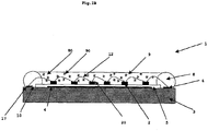
- FIG. 1A shows an LED module 1 (hereinafter also called module) according to an embodiment of the invention.
- the module 1 has at least one light-emitting diode (LED die or LED chip) 2.
- the number of LED chips 2 is not limited by the invention.
- the LED chip 2 preferably has a height of 50 to 500 ⁇ m, preferably 100 to 200 ⁇ m.
- the LED chips 2 are applied to the carrier 3. Amber, red, green and / or blue LED chips 2 (for example RGB) or blue and red LEDs can be used as LED chips 2 for generating monochromatic, white or differently colored, mixed light. Furthermore, the LED chip 2 can be arranged with a photoluminescent material arranged above the LED chip 2, such as, for example, inorganic phosphor (e. G.
- Grenades YAG: Ce 3+ , LuAG: Ce 3+ ; orthosilicates (BOSE): (approx , Sr, Ba) 2 SiO 4 : Eu 2 +, (Ca, Sr) 2 SiO 4 : Eu 2+ , (Sr, Ba) 2 SiO 4 : Eu 2+ , (Ca, Ba) 2 SiO 4 : Eu 2+ ; Nitrides: CaAlSiN 3 : Eu 2+ , (Sr, Ca) AlSiN 3 : Eu 2+ , CaAlSiON 3 : Eu 2+ , ⁇ -SiAlON: Eu 2+ )) and / or organic phosphor (s), can be provided by means of of which the light emitted by the LED chip 2 and the light converted in the photoluminescent material are mixed with one another in such a way that any desired color or white light (for example by means of blue LED and yellow (and / or green and / or red) phosphor ) can be
- the module 1 consists of a carrier 3 and a preferably structured metallic layer 4.
- the carrier 3 is preferably a printed circuit board, the carrier 3 consisting of a metal core, preferably an aluminum plate, and an electrically insulating dielectric and structured copper conductor tracks.
- the metallic layer 4 is applied to the carrier 3; the carrier 3 is preferably coated with the metallic layer 4.
- the metallic layer 4 is preferably a silver layer, a gold layer, an ENIG (Electroless Nickel / Immersion Gold), an ENEPIG (Electroless Nickel / Electroless Palladium / Immersion Gold) or an ENEC / OSP (Electroless Ni / Electroless Cu / OSP (Organic Surface Protection)) and preferably covers the entire surface of the carrier.
- the metallic layer 4 can consist of a surface that can be bonded or at least partially bondable, whereby in the non-bondable surface regions this can additionally be protected against change by oxides or organic layer (s).
- the layer 4 preferably has a thickness of 30 to 8000 nm, particularly preferably a thickness of 100 to 300nm or 2000 to 6000nm. This upper limit is partly technical, but also due to the cost of the silver or gold material as a compromise. According to the invention, thicker / thicker coatings are also conceivable.
- a lacquer layer 5 can be provided, for example, from a highly reflective white paste in such a way that it at least essentially covers the metallic layer 4.
- the lacquer layer 5 is applied to the carrier 3, more precisely the metallic layer 4 of the carrier 3; preferably by means of a dispensing process or a screen printing process.
- the lacquer layer 5 in this embodiment preferably has a thickness or average thickness of 5 to 250 ⁇ m, more preferably 20 to 200 ⁇ m, particularly preferably 100 to 150 ⁇ m.
- the lacquer layer 5 can be realized as a (highly) reflective ceramic white layer or as a white (highly) reflective coating.
- the lacquer layer 5 is preferably a white coating preferably contains pigments made of titanium dioxide (a polymorph of TiO 2, for example TiO 2 (B)), aluminum oxide (Al 2 O 3 ), zirconium dioxide (ZrO 2 ), barium titanate (BaTiO 3 ), silicon dioxide (SiO 2 ), or potassium octatitanate (K 2 Ti 8 O 17 ).
- the pigments preferably consist of a mixture of TiO 2 and / or TiO 2 (B) and / or K 2 Ti 8 O 17 and / or SiO 2 .
- the dispersion further preferably contains an organic (for example ether (s), branched polymeric siloxane (s), preferably methyl and / or hydroxy terminated silsesquioxanes) and / or an inorganic solvent for example.
- an organic for example ether (s), branched polymeric siloxane (s), preferably methyl and / or hydroxy terminated silsesquioxanes
- an inorganic solvent for example. Water.
- the use of a mixture of organic and inorganic solvents is also feasible.
- the at least one LED chip 2 is on the metallic layer 4 (possibly with the previously described one Protective coating) directly applied and electrically contacted (e.g. in a recess of a (FR4) printed circuit board).
- the LED chip 2 can be attached in accordance with a chip-on-board (COB) technology.
- the LED chip 2 can also be applied to the carrier 3 or the lacquer layer 5 (as Figure 1B , 1C ) be. If the LED chip 2 is applied to the metallic layer 4, the lacquer layer 5 is applied only in areas on the metallic layer 4 outside of the LED chip 2.
- the lacquer layer 5 is then preferably applied to the metallic layer 4 before the LED chips 2 are applied to the metallic layer 4.
- the lacquer layer 5 is provided for this purpose in such a way that free spaces 6 remain. In these free spaces 6, the LED chip 2 is applied to the metallic layer 4.
- the distance between the side wall 20 of the LED chip 2 and the lacquer layer 5 is preferably in a range between 50 and 500 ⁇ m, particularly preferably between 100 and 300 ⁇ m.
- the LED chip 2 is preferably glued to the metallic layer 4 by means of an adhesive (not shown).
- the adhesive can be a reflective, preferably white adhesive.
- the adhesive at least partially or completely fills a gap 7 between the side wall 20 of the LED chip 2 and an edge boundary 50 of the ceramic lacquer layer 5 facing the LED chip 2, so that in the latter case the metallic layer 4 completely the lacquer layer 5, the LED chips 2 and the adhesive is covered.
- the adhesive is transparent.
- the module 1 can furthermore have a dam 8 which laterally surrounds the LED chip 2 or the plurality of LED chips 2 and which is at least partially applied to the metallic layer 4 and / or the lacquer layer 5.
- the dam 8 is preferably provided laterally spaced from the LED chip 2.
- a central filling 9 preferably fills the space 80 surrounded by the dam 8.
- the central filling 9 preferably fills the entire volume delimited by the dam 8; the interior 80 formed by the dam 8 is thus preferably filled with the filling 9 up to the highest extent of the dam 8.
- the dam 8 is made higher than the LED chip 2 and consequently projects above it in height, then the top 21 of the LED chip 2 can be covered or coated with the filling material; at least when the volume delimited by the dam 8 is completely filled with the central filling 9.
- the height of the dam 8 is preferably at least two or three times the height of the LED chip 2.
- the dam 8 preferably has a height of 0.1 to 3 mm, particularly preferably 0.25 to 2 mm, most preferably 0.5 up to 1mm.
- the diameter of the cross-sectional area of the dam 8, ie the average thickness of the dam 8 or the maximum distance between the inner wall and the outer wall of the dam 8, corresponds essentially to the height of the dam 8.
- the central filling 9 is preferably made from a matrix material, particularly preferably from a transparent, preferably liquid and temperature-curable polymer or resin or a polymer mixture.
- the central filling 9 preferably has color conversion particles and / or scattering particles 90.
- the material of the dam 8 and the material of the central filling 9 are of the same material class, preferably based on silicone.
- the dam 8 and the central filling 9 can for example be made of a polymer with the same structure. This makes it possible to apply the dam 8 and the filling 9 both in one hardening step, as will be described below.
- the rheological characteristics of the liquid polymer material for building up the wall of the dam 8 must be selected in such a way that the uncured polymer or resin is dimensionally stable until it has cured until it is cured. This approximately solid-like state can be achieved by appropriate admixture of suitable fillers.
- pyrogenic silica silicon dioxide; SiO 2
- other particulate materials fine-grained materials
- At least the inner wall of the dam can be coated with metal or the dam can be made of metal.
- isolation problems may occur with this embodiment.
- the dam 8 alternatively or additionally has (highly) reflective and / or effectively scattering particles with low absorption, such as white pigments.
- white pigments are made, for example, from TiO 2 , BaTiO 3 , BaSO 4 and / or ZrO 2 .
- These reflecting particles are preferably continuously in the mass of the dam 8.
- the dam 8 can contain 10 to 60 percent by weight of the reflecting particles.
- the entire material of the dam 8 will have a non-transparent and preferably white appearance.
- the reflection of light from the LED chip 2 occurs on the inner surface of the dam 8, whereby light is reflected back into the interior of the dam 8 and away from the LED chip 2.
- the dam 8 has the role of a reflector applied in a liquid state on the carrier 3 or the metallic layer 4 or the lacquer layer 5.
- the dam 8 can be applied using dispensing techniques, as described below. However, it is also possible that the dam 8 is a prefabricated element, preferably made of a polymer, ceramic, metal or another plastic. This element can then, for example, be glued in place.
- the dam 8 preferably has the cross-sectional shape of a semicircle, a circle, a rectangle or a square or a polygon.
- the dam 8 In the plan view, that is to say seen perpendicular to the support 3, the dam 8 has a circular, oval, ellipsoidal or angular shape, for example a rectangular or square or polygonal shape.
- the term "dam" is not a limitation on the shape as long as the dam 8 can serve as a dam 8 surrounding the inner central filling 9, and the dam 8 is made of a polymer or resin material , this is already stable in the uncured state.
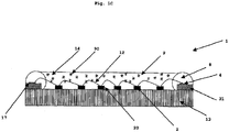
- Figure 1B represents a first illustrative example not belonging to the invention.
- the metal layer 4 only partially covers the carrier 3, the areas under the LED chips 2 and the bond pads 11 (not shown) are preferably covered with the metal layer 4. This results in the areas 10 on the carrier 3 that are not covered by the metal layer 4.
- the lacquer layer 5 covers the metal layer 4 below the LED chips 2, but not the metal layer 4 applied to the bond pads 11.
- the lacquer layer 5 extends down to the carrier surface 17 under the dam 8.
- the lacquer layer 5 preferably completely covers the surface of the carrier 3 under the dam 8. However, the lacquer layer can be applied incompletely to the carrier region under the dam 8.
- the lacquer layer 5 preferably has a thickness or average thickness of 10 to 100 ⁇ m, particularly preferably 20 to 50 ⁇ m.
- the LED chips 2 lie directly on the lacquer layer 5.
- the LED chips 2 are electronically connected to one another with bond wires 12 and to the bond pads 11.
- the ribbon wires 12 are partially mechanically protected by the dam 8 because they are partly below the dam 8.
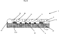
- the carrier 3 with layer 4 can also be used in addition to the examples mentioned 1C (Second illustrative example not belonging to the invention) can be constructed as follows, the structure described below also taken on its own, that is to say without the further features described in the context of the application, in the same or other areas of printed circuit board technology as advantageous (highly) reflective PCB can be used.
- a base material or base substrate 13 for example aluminum plate or gold plate
- This layer preferably has a thickness of 30 to 8000 nm.
- This high-purity aluminum layer can in turn preferably be provided in the manner described above with at least one layer of oxides, which is likewise preferably vapor-deposited.
- the printed circuit board 31 and the layer 4 are partially or preferably completely (as shown) arranged within the dam 8, so that the dam 8 does not (as shown) or only partially covers these components.
- each bond wire 12, and in particular also the one closest to the dam 8 runs completely within the volume delimited to the outside by the dam 8.
- the dam 8 is therefore preferably seated directly and completely on the base substrate 13.
- Base substrate 13 and circuit board 31 form the carrier 3 in the embodiments shown on the 1B-1C and Fig. 4 .
- the printed circuit board 31 and the base substrate 13 can be connected with the aid of an additional substrate 16, for example by an adhesive process or a soldering process (see Fig. 4 ).
- the electrically insulating base or carrier material (usually epoxy resin-impregnated glass fiber mats) of the printed circuit board 31 has a thickness of 30 to 300 ⁇ m, particularly preferably 100 ⁇ m.
- the copper layer (conductor tracks) applied to the carrier material of the (FR4) printed circuit board 31 preferably has a thickness of 18 to 140 ⁇ m, particularly preferably 60 to 90 ⁇ m.
- the finishing surface / metal layer 4 consists of nickel and / or palladium and / or gold (as mentioned earlier, for example ENIG, ENEPIG or ENEC / OSP).
- the metal layer 4 is preferably applied to the surface of the (FR4) printed circuit board 31 (of the carrier 3) under the dam 8.
- the solder mask is preferably white.
- the printed circuit board 31 also preferably has at least one recess 14 (e.g. bore, milling, etc.) in an area in which the LED chip or chips 2 are provided.
- These recess (s) 14 release the underlying aluminum layer or coated aluminum plate (or gold layer) and represent a reflective surface on the (coated) base substrate 13.
- the LED chip 2 can the LED chips 2 are applied directly to the base substrate 13 in the manner described (if appropriate with the above-described protective coating made of oxides).
- a carrier 3 or a printed circuit board can be provided, which enables a high robustness (and thus a certain indestructibility) of the construction.
- the problems associated with the use of silver including the comparatively high cost of silver, are avoided.
- a lacquer layer 5 made from a ceramic lacquer or a ceramic highly reflective white paste can be provided in such a way that it at least partially covers the base substrate 13.
- the lacquer layer 5 can be applied to the base substrate 13; preferably by means of a screen printing process.
- the lacquer layer 5 can also be provided, for example, particularly in the area of a possible recess 14 in a (FR4) printed circuit board and, if appropriate, also cover the base substrate 13 and / or the (FR4) printed circuit board 31 (for example outside of the through a recess 14 in areas of the coated base substrate).
- the lacquer layer 5 preferably has a thickness or average thickness of 10 to 100 ⁇ m, particularly preferably 20 to 50 ⁇ m.
- a reflector 15 can be applied to the circuit board 31 outside the dam (see Fig. 4 ).
- mid- and / or low-power (0.05-0.6 W) LED chips 2 can be mounted inside the dam 8 (in the space 80 surrounding the dam) (for example, see 2A-C ).
- Use of high-power LED chips 2 is also conceivable based on the examples described.
- the LED chips 2 are preferably connected in series (structured in strands 32) (see 2A-C ).
- a strand 32 preferably contains from 5 to 20 LED chips 2, more preferably 10-14 LED chips 2, particularly preferably 12 LED chips 2.
- the LED chips 2 are preferably in 1-15 strands, more preferably in 6- 12 strands on the LED module 1 set up to achieve the shortest electrical connections between LED chips 2 and the bond pads 11.
- the LED module 1 is preferably with from 40 to 160 LED chips 2, particularly preferably from 70 to 150 LED chips 2, for example according to the illustrations 2A-C Equipped evenly and with little space to each other in order to achieve the most homogeneous light distribution possible.
- the LED module 1 can contain 10-50 LED chips 2 set up in 1-4 strands.
- the surface 18 occupied by the LED chips is, for example, from 60% to 90%, preferably 64-75% of the total surface of the room 80.
- the solutions mentioned have the advantage that when using the LED module 1 with an optical element (s) (eg reflector 15, see Fig. 4 ) and / or in a luminaire (e.g. downlight, spotlight, LED bulb, see Fig. 3 ) the homogeneous light distribution / light-emitting surface achieved by the uniform placement of the LED chips 2 is not disadvantageously reshaped.
- an optical element eg reflector 15, see Fig. 4
- a luminaire e.g. downlight, spotlight, LED bulb, see Fig. 3
- the homogeneous light distribution / light-emitting surface achieved by the uniform placement of the LED chips 2 is not disadvantageously reshaped.
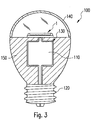
- a spotlight or a retrofit LED lamp 100 can be provided which have at least one LED module 1 according to the invention.
- "Retrofit” lamps are lamps that are designed with regard to their mechanical and electrical connections to replace existing lamps (light bulb, halogen lamp, ). According to its external appearance, it can therefore essentially have the shape of a conventional light bulb or halogen lamp and / or be equipped with a corresponding (lamp) base 120 (for example E27 or E14) or plug (not shown).
- the retrofit LED lamp also usually has its own driver circuit 110 which, for example, adapts the supply current to the operating conditions of the LEDs based on a mains voltage supplied via the base 120.
- the retrofit LED lamps 100 can thus be screwed or inserted into conventional sockets like conventional lamps and operated by means of the supplied mains current.
- the driver circuit 110 can be arranged mechanically and electrically protected in a driver housing 130 as part of a housing.
- the retrofit LED lamp 100 can have a transparent cover 140 as a further part of the housing, which has a glass bulb a conventional light bulb or halogen lamp is simulated.
- heat is generated by the LED module 1 and also by the driver circuit 110. This heat is generally removed (as a further part of the housing) via a heat sink 150 thermally connected to the LED module 1 and the driver circuit 110.
- the LED lamp 100 can also have further electrical, electronic and / or mechanical components, such as, for example, a reflector for the targeted emission of light, a sensor system for measuring and controlling the LED module 1 and other known features of a ballast and / or to emit and / or change the light.
- the geometry of the dam 8 is preferably circular in plan view, other geometries defined by the dam 8 are also possible, such as, for example, rectangular shapes, etc.
- the diameter of the circular dam is preferably from 17 to 28 mm, more preferably from 19 to 26 mm.
- a metallic layer 4 preferably a silver layer (or gold layer) with a thickness of approximately 30 to 8000 nm is applied to a carrier 3 (for example a printed circuit board).
- carrier 3 for example a printed circuit board
- this is provided with a further (protective) layer of oxides.
- Carrier 3 and metallic layer 4 can also consist of a base substrate consisting of aluminum plate with vapor-deposited high-purity aluminum layers and optionally layers of oxides onto which a (FR4) printed circuit board 31 is laminated, which preferably has recesses which the base substrate 13 release at least in places, in which or later on the LED chips 2 can be placed.
- a ceramic lacquer (“ink”) is applied to the carrier 3 - more precisely to the metallic layer 4 of the carrier 3, for example by means of a screen printing process.
- the ceramic lacquer is provided in such a way that the metallic layer 4 of the carrier 3 is at least partially, preferably completely, covered by the lacquer layer 5 formed. It is conceivable that this step is repeated several times (any number of times) in order to increase the layer thickness of the lacquer.
- the lacquer layer 5 has a thickness of approximately 15 to 20 ⁇ m, for example.
- the thickness of the lacquer layer 5 can be increased to a range of, for example, 40 to 50 ⁇ m or more by repeated printing.
- the reflectance of the lacquer layer 5 increases from, for example, 80% at 18 pm to approximately 95% at 40 to 50 ⁇ m. This degree of reflection applies when measuring the paint layer on a black background.
- the light of the LED chip 2 passing through the lacquer layer 5 can be reflected back due to the underlying metallic layer or silver layer 4.
- This double-reflective configuration has the advantage that, for example in the event of an oxidative blackening of the silver layer 4, a substantial proportion of the light is still reflected by the lacquer layer 5 above, which increases the efficiency of the module 1.
- the lacquer layer 5 can also serve as protection against oxidation for the metallic layer 4, so that its reflection properties are essentially retained during the service life of the module 1.
- the lacquer layer 5 applied to the metallic layer 4 is provided according to the invention in such a way that the metallic layer 4 is partially covered by the lacquer layer 5.
- partial means that the metallic layer 4 is not completely covered by the lacquer layer 5, but that free spaces 6 remain, into which the LED chips 2 are later inserted and thus applied to the metallic layer 4.
- the recesses thereof or the locations of the coated base substrate that are thereby exposed preferably at least partially coincide with the clearances 6 into which the LED chips 2 preferably onto the coated base substrate and thus can be applied to the metallic layer 4.
- At least one or more LED chip (s) 2 placed on the metallic layer 4 in the free spaces 6 of the lacquer layer 5; so applied, and electrically contacted.
- the LED chip 2 is preferably attached in accordance with chip-on-board (COB) technology or also as an SMD LED.
- COB chip-on-board
- the bond wires 12 are, for example, in Figure 2A-C shown. However, in configurations outside of the invention, it is also conceivable for the LED chips 2 to be placed on the lacquer layer 5, should the latter cover the entire metallic layer 4.
- the LED chip 2 can also be provided directly on the carrier 3.
- the LED chip 2 is preferably first applied to the carrier 3, so that after the coating it is laterally surrounded by the metallic layer 4 and the lacquer layer 5; the LED chip 2 is then of course not coated in the radiation direction (in particular on its upper side 21).
- the LED chips 2 are preferably glued, particularly preferably glued to the metallic layer 4 or base substrate 13.
- a reflective, preferably white adhesive can advantageously be used.
- the metering of the adhesive should be selected such that when the LED chip 2 is placed on the adhesive, for example in the free spaces 6 of the lacquer layer 5, the latter is laterally displaced such that there is a possibly remaining gap 7 between the side wall 20 of the LED chip 2 and an edge boundary 50 facing the LED chip 2 of the ceramic lacquer layer 5 / the free space 6 (possibly also the metallic layer 4) at least partially or completely, so that the metallic layer 4 (and possibly also the laminated (FR4) circuit board) is completely covered in the latter case.
- a double-reflective configuration can thus also be achieved in areas close to LED chip 2 and over the entire area of module 1 or carrier 3.
- a dam 8 is applied or provided at least partially on the metallic layer 4 (possibly including any laminated (FR4) printed circuit board present) and / or the lacquer layer 5 in such a way that the dam 8 Chips 2 surrounds laterally.
- the dam 8 is preferably formed as an annular dam (for example a torus).
- the dam 8 made of a liquid polymer or resin or a polymer mixture is preferably applied around the LED chips 2 on the metallic layer 4.
- the dam 8 can also at least partially extend over the preferably printed ceramic lacquer layer 5.
- ring or "ring-shaped” in the context of the present description and the claims does not limit the contour of the Walls of the dam 8; e.g. B. the ring does not necessarily have to have a circular shape, but can for example have the shape of a square, an oval, an ellipse or a rectangle etc.
- the circular shape is preferred because of the proximity to circular reflectors, since the plurality of LEDs preferably appear as a single round optical element.
- a square shape is preferred in terms of production technology due to the simpler arrangement.
- a flat plate is preferably used as carrier 3 without depressions, since the reflective effect of walls of a depression can be achieved through the dam walls.
- the cross-sectional shape of the dam 8 can be controlled by the diameter of the dispensing needle used, the flow characteristics of the liquid dam material and the flow (dispensing) speed. Due to the dispensing technology, for example, the cross section of the dam 8 to the summit of the dam 8 can have a tapering shape. As a result, the inner surface of the dam 8 is chamfered and preferably steeper at its upper part, which can be advantageous for reflection purposes.
- the dam 8 can also be produced by means of so-called overmoulding. If this can then no longer be used to protect the wirebonds, the emitting surface increases slightly.
- the dam 8 can also be provided as a prefabricated element, which is preferably made of a polymer or resin, ceramic, metal or another plastic, for example as an injection molded part.
- the space surrounded by the dam 8 is filled with a filling material.
- the volume delimited by the inner walls of the inherently stable ring 8 is filled with a liquid filling material.
- this central filling 9 is preferably made such that the top of the filling 9 is flush with the top of the walls of the dam 8.
- the central filling 9 is particularly preferably provided such that it completely covers or coats the upper side of the LED chip 2.
- the central filling 9 also covers the space between the LED chip 2 and the walls of the dam 8 and touches the lacquer layer 5 and, via free space 6 in the lacquer, the metallic layer (silver layer or high-purity aluminum layer or the like) 4 or the one for applying the LED Chips 2 used glue. Due to the preferred filling with a liquid polymer or resin, the top of the central filling 9 will preferably be flat.
- Liquid unhardened polymer or resin for example silicone
- the materials of the dam 8 and the central filling 9 are preferably similar or the same, so that they are preferably chemically identical.
- the chemical identity should be such that the material used for the dam 8 and the central fill 9 can each be hardened using the same hardening mechanism in order to preferably establish a chemical and / or physical bond between the two materials across their interface .
- the materials of the dam 8 and the central filling 9 can be different; the material of the dam 8, which is preferably identical to the material of the central filling, can also be provided with different 'additives' than the material of the central filling 9.
- the material of the dam 8 which is preferably identical to the material of the central filling, can also be provided with different 'additives' than the material of the central filling 9.
- 9 color conversion particles can be added to the filling material of the central filling for white color conversion LED modules.
- the type and the amount of the color conversion particles depend on the desired color temperature of the LED module 1, which as such are known from the prior art. There is preferably an increasing concentration gradient of the color conversion particles from top to bottom, which z. B. can be achieved by lowering the color conversion particles to the bottom of the filling 9.
- the dam 8 and the central filling 9 are made of a liquid polymer or resin or a polymer mixture, this is preferably hardened after the application or filling.
- the step of applying the dam 8 and filling the dam 8 with the filling material thus preferably further comprises hardening the dam 8, which is preferably made of a liquid polymer / polymer mixture, or hardening the filling material, preferably made of a liquid polymer / polymer mixture, of the central one Filling 9.
- the hardening of the dam 8 and the hardening of the central filling 9 can be carried out after the respective steps for providing the dam 8 and the central filling 9 - that is to say independently of one another.
- This manufacturing process is based on a comparatively high mechanical stability of the material of the wall of the dam 8 in the uncured 'liquid' state.
- additional filling materials such as silicones, can in turn be added to the material of the dam 8.
- the joint hardening of the dam 8 and the central filling 9 consequently has the advantage that polymerization can take place between the dam material and the matrix material of the central filling 9.
- a standardized computer-controlled delivery device can be used both for the manufacture of the dam 8 and for the filling 9.
- the LED chips 2 are first applied to the carrier 3 and then the carrier 3 (except the LED chips 2) is coated with the metallic layer 4 and then the lacquer layer 5 is applied.
- the only decisive factor is that the combination of lacquer layer 5 and metallic layer 4 forms a double reflective effect for the light emitted by the LED chip 2, so that the light of the LED chip 2 passing through the lacquer layer 5 due to the underlying metallic ( Silver) layer 4 reflected back is and thus the efficiency of module 1 is increased.
- the module 1 can also be generally designed, for example, as an electronic or optoelectronic module and have other electronic or optoelectronic components instead of an LED chip.
- module 1 can be designed as a light-erasable memory device, such as an EEPROM.
- the invention can also be used for light-sensitive sensors, such as RGB sensors, infrared sensors or CCD sensors. Infrared emitters and light-sensitive light detection devices are also areas of application, in particular if the sensor is present as a bare chip in the COB or carrier strip technology (lead frame).
- the coating can also be used in connection with light guides and optical fibers.
- An optical fiber, to which light from the light source 2 is to be transmitted, is preferably arranged at a distance from and in front of the light source 2 and extends, for example, out of the filler material 9 away from the light source 2.
- the module 1 can be provided with a mechanical fastening for the optical fibers. Such an arrangement provides improved light transmission from the light source 2 to the optical fiber.
Description
Die vorliegende Erfindung betrifft ein LED-Modul mit einem Träger und wenigstens einem LED-Chip und ein Verfahren zum Herstellen eines solchen LED-Moduls.The present invention relates to an LED module with a carrier and at least one LED chip and a method for producing such an LED module.
Aus dem Stand der Technik sind LED-Module der eingangs genannten Art bekannt. So zeigt bspw. die
Ferner zeigt die
Es ist somit eine Aufgabe der Erfindung, ein einfaches LED-Modul sowie als auch ein Verfahren zum Herstellen eines solchen LED-Moduls bereitzustellen, welches einen hohen Reflexionsgrad des Trägers ermöglicht und gleichzeitig eine verbesserte Wärmeabfuhr aufweist.It is therefore an object of the invention to provide a simple LED module and also a method for producing such an LED module, which enables a high degree of reflection of the carrier and at the same time has improved heat dissipation.
Diese Aufgabe wird durch die Merkmale der unabhängigen Ansprüche gelöst. Die abhängigen Ansprüche bilden den zentralen Gedanken der Erfindung in besonders vorteilhafter Weise weiter.This object is solved by the features of the independent claims. The dependent claims form the central one The idea of the invention is particularly advantageous.
Gemäß einem ersten Aspekt der Erfindung wird ein LED-Modul vorgeschlagen, welches einen Träger aufweist, z.B. eine Leiterplatte, wobei auf dem Träger eine metallische Schicht aufgebracht ist. Das LED-Modul weist wenigstens einen LED-Chip sowie eine die metallische Schicht wenigstens teilweise überdeckende, auf dem Träger aufgebrachte Lackschicht, beispielsweise aus einem keramischen Lack auf. Der LED-Chip (oder die SMD-LED) kann bspw. auf der Leiterplatte bzw. der metallischen Schicht (oder der Lackschicht) gemäss einer Chip-on-board (COB) Technologie befestigt sein. Die Verwendung der SMD (Surface-mounted device) Technologie ist alternativ auch denkbar.According to a first aspect of the invention, an LED module is proposed which has a carrier, e.g. a printed circuit board, a metallic layer being applied to the carrier. The LED module has at least one LED chip and a lacquer layer which at least partially covers the metallic layer and is applied to the carrier, for example from a ceramic lacquer. The LED chip (or the SMD LED) can, for example, be attached to the circuit board or the metallic layer (or the lacquer layer) according to a chip-on-board (COB) technology. The use of SMD (surface-mounted device) technology is alternatively also conceivable.
Erfindungsgemäß kann das durch die Lackschicht hindurchgehende Licht des LED-Chips aufgrund der darunter liegenden metallischen Schicht zurückreflektiert werden. Diese doppelt reflektive Ausgestaltung Lackschicht/Metallschicht hat den Vorteil, dass beispielsweise bei einer oxidativen Schwärzung der Metallschicht (bspw. Silberschicht) immer noch ein wesentlicher Anteil des Lichts durch die darüber liegende Lackschicht reflektiert wird, was den Wirkungsgrad des Moduls steigert. Gleichzeitig ist die Wärmeleitfähigkeit des Moduls durch die Anwendung der erfindungsgemäßen Metallschicht verbessert.According to the invention, the light of the LED chip passing through the lacquer layer can be reflected back due to the underlying metallic layer. This double reflective design of the lacquer layer / metal layer has the advantage that, for example, in the case of an oxidative blackening of the metal layer (e.g. silver layer), a substantial proportion of the light is still reflected by the lacquer layer above, which increases the efficiency of the module. At the same time, the thermal conductivity of the module is improved by using the metal layer according to the invention.
Erfindungsgemäß ist der LED-Chip auf der metallischen Schicht aufgebracht. Die Lackschicht ist dann in Bereichen auf der metallischen Schicht außerhalb des LED-Chips aufgebracht. Folglich weist die Lackschicht Freistellen auf, in die die LED-Chips eingesetzt und auf die metallische Schicht aufgebracht werden können.According to the invention, the LED chip is applied to the metallic layer. The lacquer layer is then applied in areas on the metallic layer outside the LED chip. As a result, the lacquer layer has clearances in which the LED chips can be inserted and applied to the metallic layer.
Der LED-Chip kann auf die metallische Schicht mittels eines Klebers geklebt sein. Der Kleber kann beispielsweise ein transparenter durchscheinender Kleber oder ein reflektierender, also insbesondere weißer Kleber sein. Vorzugsweise füllt der Kleber eine Lücke zwischen der Seitenwand des LED-Chips und einer dem LED-Chip zugewandten Randbegrenzung der keramischen Lackschicht wenigstens teilweise oder vollständig aus, so dass die Metallschicht (bspw. Silberschicht) im letztgenannten Fall vollständig abgedeckt ist. Ist der Kleber aus einem lichtreflektierenden Material, so kann die gesamte Trägeroberfläche mit einer doppelt reflektiven Ausgestaltung ausgebildet werden.The LED chip can be glued to the metallic layer using an adhesive. The adhesive can be, for example, a transparent, translucent adhesive or a reflective, in particular white, adhesive. The adhesive preferably fills at least partially or completely a gap between the side wall of the LED chip and an edge boundary of the ceramic lacquer layer facing the LED chip, so that the metal layer (for example silver layer) is completely covered in the latter case. If the adhesive is made of a light-reflecting material, the entire carrier surface can be designed with a double reflective design.
Der Abstand zwischen der Seitenwand des LED-Chips und der Lackschicht liegt vorzugsweise in einem Bereich zwischen 50 und 500µm, besonders vorzugsweise zwischen 100 bis 300µm.The distance between the side wall of the LED chip and the lacquer layer is preferably in a range between 50 and 500 μm, particularly preferably between 100 and 300 μm.
Die Lackschicht kann eine mittlere Dicke von 10 bis 100µm, vorzugsweise eine mittlere Dicke von 20 bis 50µm aufweisen.The lacquer layer can have an average thickness of 10 to 100 µm, preferably an average thickness of 20 to 50 µm.
Die metallische Schicht kann eine Stärke von 30 bis 8000nm aufweisen, vorzugsweise eine Stärke von 100 bis 300nm oder 2000 bis 6000nm. Im Falle einer Silberschicht hat diese vorzugsweise eine Stärke bzw. mittlere Dicke von 3000 bis 5000nm. Im Falle einer Goldschicht hat diese vorzugsweise eine Stärke bzw. mittlere Dicke von 30 bis 100nm.The metallic layer can have a thickness of 30 to 8000 nm, preferably a thickness of 100 to 300 nm or 2000 to 6000 nm. In the case of a silver layer, this preferably has a thickness or average thickness of 3000 to 5000 nm. In the case of a gold layer, this preferably has a thickness or average thickness of 30 to 100 nm.
Das LED-Modul kann weiterhin einen den LED-Chip bzw. mehrere LED-Chips seitlich umgebenden und die LED-Chips vorzugsweise in der Höhe überragenden Damm aufweisen, welcher wenigstens teilweise auf der metallischen Schicht und/oder der Lackschicht aufgebracht ist.The LED module can furthermore have a dam which laterally surrounds the LED chip or a plurality of LED chips and preferably extends above the height of the LED chips and which is at least partially applied to the metallic layer and / or the lacquer layer.
Vorzugsweise weist das LED-Modul ferner eine zentrale Füllung aus einem Matrixmaterial auf. Das Matrixmaterial kann ein transparentes und vorzugsweise flüssiges und durch Temperatur härtbares Polymer sein; z.B. Silikon. Die zentrale Füllung füllt vorzugsweise den von dem Damm umgebenden Raum (vollständig) aus. Besonders vorzugsweise ist dabei die Oberseite des LED-Chips bedeckt bzw. beschichtet.The LED module preferably also has a central filling made of a matrix material. The matrix material can be a transparent and preferably liquid and thermosetting polymer; e.g. silicone. The central filling preferably fills (completely) the space surrounding the dam. The top side of the LED chip is particularly preferably covered or coated.
Die zentrale Füllung kann folglich das gesamte durch den Damm begrenzte Volumen ausfüllen, so dass die Oberseite der Füllung auf derselben Ebene wie die maximale Höhe des Dammes liegt. Vorzugsweise ist der Damm, also die Damm-Oberkante, höher als der LED-Chip (d.h. dessen Oberkante), so dass dann die Oberseite des LED-Chips beschichtet bzw. von der Füllung abgedeckt und geschützt ist.The central fill can therefore fill the entire volume delimited by the dam, so that the top of the fill is on the same level as the maximum height of the dam. The dam, i.e. the upper edge of the dam, is preferably higher than the LED chip (i.e. its upper edge), so that the upper side of the LED chip is then coated or covered and protected by the filling.
Die zentrale Füllung kann Farbkonversionspartikel/Leuchtstoffpartikel aufweisen, welche Licht, das von einem LED-Chip emittiert wird, in Licht eines zweiten, geringeren Frequenzspektrums verändert. Alternativ oder zusätzlich kann die zentrale Füllung Streupartikel aufweisen, welche Licht, das von einem LED-Chip emittiert wird, streut, um dadurch eine homogenere Emission zu ermöglichen.The central filling can have color conversion particles / phosphor particles, which change light, which is emitted by an LED chip, into light of a second, lower frequency spectrum. Alternatively or additionally, the central filling can have scattering particles, which scatter light that is emitted by an LED chip, in order to thereby enable a more homogeneous emission.
Das Material des Dammes und das Material der zentralen Füllung können von der gleichen Materialklasse sein, vorzugsweise auf Silikonbasis. Besonders vorzugsweise sind der Damm und die zentrale Füllung aus einem Polymer bzw. Harz mit derselben Struktur hergestellt, wodurch es ermöglicht wird, den Damm und die Füllung beide in einem Härtungsschritt aufzubringen bzw. auszuhärten. Besonders vorzugsweise haben das Material bzw. das Polymer des Dammes und der zentralen Füllung eine ähnliche chemische Struktur welche vorzugsweise eine Quervernetzung zwischen den Materialien erlaubt. Sie können auch durch die gleiche Reaktion polymerisiert werden und sich nur durch die sich ergebende Shore Härte unterscheiden, z.B. für den Damm eine ShoreA Härte von 70 und für die Füllung eine ShoreA Härte von 35. Sie können auch aus einem identischen Material hergestellt sein, welches bspw. nur durch die verwendeten Füllstoffe zu einer unterschiedlichen funktionellen Ausprägung gelangt.The material of the dam and the material of the central filling can be of the same material class, preferably silicone-based. The dam and the central filling are particularly preferably made of a polymer or resin having the same structure, which makes it possible to apply or harden both the dam and the filling in one hardening step. The material or the polymer of the dam and the central filling particularly preferably have a similar chemical structure which preferably allows cross-linking between the materials. They can also be polymerized by the same reaction and differ only in the resulting Shore hardness, for example a ShoreA for the dam Hardness of 70 and a ShoreA hardness of 35 for the filling. They can also be made of an identical material, which, for example, only achieves a different functional expression through the fillers used.
Wie zuvor beschrieben, kann auch der Damm aus einem Harz oder einem Polymermaterial hergestellt sein. Unterschiedliche Basisharze können für den Damm benutzt werden. Bevorzugte Materialien sind Silikone, aufgrund ihrer hohen UV-Stabilität. Das Material des Dammes kann Füllstoffe in Form von partikelförmigem Material wie z.B. pyrogener Kieselsäure (Siliziumdioxid; SiO2) aufweisen, wobei partikelförmiges Material oder fein granuliertes Material verwendet werden kann, um die gewünschten rheologischen Eigenschaften des ungehärteten Polymers zu bestimmen. Das Damm-Material ist vorzugsweise für die Wellenlänge des Lichtes, welches durch die zentrale Füllung innerhalb des Dammes dringt, nicht transparent (bzw. hoch reflektierend). Eine transparente oder durchscheinende Ausprägung des Dammes ist gemäß einer alternativen Ausführungsform der Erfindung denkbar.As previously described, the dam can also be made of a resin or a polymer material. Different base resins can be used for the dam. Preferred materials are silicones due to their high UV stability. The material of the dam can be fillers in the form of particulate material such as e.g. have fumed silica (silicon dioxide; SiO2), whereby particulate material or finely granulated material can be used to determine the desired rheological properties of the uncured polymer. The dam material is preferably not transparent (or highly reflective) for the wavelength of the light that penetrates through the central filling within the dam. A transparent or translucent design of the dam is conceivable according to an alternative embodiment of the invention.
Zumindest die innere Wand des Dammes kann lichtreflektierend/streuend sein. Besonders vorzugsweise weist der Damm Licht streuende Partikel, wie zum Beispiel weiße Pigmente (z.B. SiO2, TiO2, BaTiO3, SnO, ZrO2), auf. Diese reflektierenden/streuenden Partikel befinden sich vorzugsweise durchgehend in der Masse des Damms. Dadurch hat der Damm die Rolle eines in einem flüssigen Zustand auf eine (Leiter-)Platte aufgebrachten Reflektors. Der Damm kann 10 bis 60 Gewichtsprozent, besonders bevorzugt 20 bis 40 Gewichtsprozent der reflektierenden Partikel enthalten.At least the inner wall of the dam can be light reflecting / scattering. The dam particularly preferably has light-scattering particles, such as white pigments (e.g. SiO2, TiO2, BaTiO3, SnO, ZrO2). These reflecting / scattering particles are preferably continuously in the mass of the dam. As a result, the dam has the role of a reflector applied to a (printed circuit board) in a liquid state. The dam can contain 10 to 60 percent by weight, particularly preferably 20 to 40 percent by weight, of the reflective particles.
Der Damm kann ein vorgefertigtes Element sein, vorzugsweise aus einem Polymer (z.B. gefüllter Polymer/Harz), Keramik, Metall oder einem anderen (vorzugsweise gefüllten) Kunststoff.The dam can be a prefabricated element, preferably made of a polymer (eg filled polymer / resin), ceramic, Metal or another (preferably filled) plastic.
Der Damm kann eine Höhe von 0,1mm bis 3mm haben, vorzugsweise 0,25mm bis 2mm, besonders vorzugsweise 0,5 bis 1mm.The dam can have a height of 0.1 mm to 3 mm, preferably 0.25 mm to 2 mm, particularly preferably 0.5 to 1 mm.
Der Durchmesser der Querschnittsfläche des Dammes, also die durchschnittliche Dicke des Dammes bzw. der maximalen Abstand zwischen der inneren Wand und der äußeren Wand des Dammes, kann gemäß den Anforderungen des endgültigen Elementes gewählt werden. Vorzugsweise entspricht die Dicke im Wesentlichen der Höhe des Dammes. Bei einem Gesamtdurchmesser des Dammes von ungefähr 5mm kann dessen Dicke gleich oder weniger als 0,5mm sein. Für größere Durchmesser ist die Dicke entsprechend auf mehr als 0,5mm abgestimmt, wobei bei geringeren Durchmessern die Dicke auch weniger als 0,5mm sein kann.The diameter of the cross-sectional area of the dam, ie the average thickness of the dam or the maximum distance between the inner wall and the outer wall of the dam, can be chosen according to the requirements of the final element. The thickness preferably corresponds essentially to the height of the dam. With a total diameter of the dam of approximately 5 mm, its thickness can be equal to or less than 0.5 mm. For larger diameters, the thickness is correspondingly matched to more than 0.5 mm, and the thickness can also be less than 0.5 mm for smaller diameters.
Die Querschnittsform des Dammes ist nicht durch die Erfindung beschränkt.The cross-sectional shape of the dam is not limited by the invention.
Der Damm kann in der Draufsicht, also senkrecht zum Träger bzw. der Leiterplatte gesehen, eine kreisförmige, ellipsoide, ovale, oder eckige bzw. polygone Form, beispielsweise eine rechteckige oder quadratische oder achteckige Form, aufweisen.The dam can have a circular, ellipsoidal, oval, or angular or polygonal shape, for example a rectangular, square or octagonal shape, when viewed from above, that is to say perpendicular to the support or the printed circuit board.
Die Erfindung bezieht sich ferner auf ein Spotlight, ein Downlight oder eine Retrofit LED-Lampe, welche wenigstens ein LED-Modul gemäß der Erfindung aufweisen.The invention further relates to a spotlight, a downlight or a retrofit LED lamp which has at least one LED module according to the invention.
Die Erfindung bezieht sich auch auf ein LED- Modul, das herstellbar ist durch ein Verfahren zur Herstellung eines LED-Moduls. Zuerst wird eine metallische Schicht, vorzugsweise eine Silberschicht oder eine Goldschicht, auf einen Träger, insbesondere eine Leiterplatte aufgebracht. Die Schichtdicke kann dabei dadurch gesteigert werden, dass mehrere Beschichtungsschritte bzw. Beschichtungsvorgänge nacheinander durchgeführt werden.The invention also relates to an LED module that can be produced by a method for producing an LED module. First, a metallic layer, preferably a silver layer or a gold layer, is applied to one Carrier, in particular a printed circuit board applied. The layer thickness can be increased in that several coating steps or coating processes are carried out in succession.
Die reflektierende Metallschicht, insbesondere eine Silberoberfläche, kann durch Beschichtung mit Titanoxid, Aluminiumoxid oder Glas zusätzlich vor Oxidation geschützt werden. In diesem Falle dient der weiße Lack primär der Optimierung des Lichtoutputs.The reflective metal layer, in particular a silver surface, can additionally be protected against oxidation by coating with titanium oxide, aluminum oxide or glass. In this case, the white lacquer primarily serves to optimize the light output.
Danach wird ein keramischer Lack auf den Träger - genauer die metallische Schicht des Trägers - derart aufgebracht, dass diese (r) von einer Lackschicht teilweise bedeckt ist. Ist die metallische Schicht nur teilweise, also partiell bedeckt, weist die Lackschicht folglich überall dort Freistellen auf, wo kein Lack ist. Vorzugsweise wird die Lackschicht aufgedruckt, beispielsweise mittels Siebdruckverfahren.A ceramic lacquer is then applied to the carrier - more precisely the metallic layer of the carrier - in such a way that it is partially covered by a lacquer layer. If the metallic layer is only partially, i.e. partially covered, the lacquer layer consequently has clearances wherever there is no lacquer. The lacquer layer is preferably printed on, for example by means of a screen printing method.
Anschließend (oder auch vor, während oder nach einem der vorgenannten Schritte) wird wenigstens ein LED-Chip auf dem Träger, der metallischen Schicht oder der Lackschicht platziert.Subsequently (or also before, during or after one of the aforementioned steps), at least one LED chip is placed on the carrier, the metallic layer or the lacquer layer.
Der LED-Chip wird in den Freistellen der Lackschicht auf die metallische Schicht geklebt. Dies geschieht vorzugsweise mittels eines reflektierenden, besonders vorzugsweise weißen Klebers. Die Dosierung des Klebers wird vorzugsweise derart gewählt, dass beim Platzieren des LED-Chips auf den Kleber in den Freistellen der Kleber seitlich derart verdrängt wird, sodass er die verbleibende Lücke zwischen der Seitenwand des LED-Chips und einer dem LED-Chip zugewandten Randbegrenzung der keramischen Lackschicht wenigstens teilweise oder vollständig ausfüllt, so dass die metallische Schicht im letztgenannten Fall vollständig abgedeckt ist.The LED chip is glued to the metallic layer in the cut-outs of the lacquer layer. This is preferably done using a reflective, particularly preferably white, adhesive. The dosage of the adhesive is preferably selected such that when the LED chip is placed on the adhesive in the free spaces, the adhesive is laterally displaced in such a way that the remaining gap between the side wall of the LED chip and an edge limitation of the LED chip facing the LED chip ceramic lacquer layer at least partially or completely fills in, so that the metallic layer is completely covered in the latter case.
Es besteht ferner die Möglichkeit, einen Damm wenigstens teilweise auf der metallischen Schicht und/oder der Lackschicht derart aufzubringen, dass der Damm den wenigstens einen LED-Chip seitlich umgibt. Im Anschluss daran wird der von dem Damm umgebende Raum mit einem Füllmaterial zum Bilden einer zentralen Füllung ausgefüllt. Die so entstehende zentrale Füllung wird vorzugsweise derart vorgesehen, dass sie die Oberseite des LED-Chips beschichtet.There is also the possibility of applying a dam at least partially on the metallic layer and / or the lacquer layer in such a way that the dam laterally surrounds the at least one LED chip. The space surrounding the dam is then filled with a filling material to form a central filling. The resulting central filling is preferably provided such that it coats the top of the LED chip.
Der Damm und die zentrale Füllung sind vorzugsweise aus einem flüssigen Polymer oder einer flüssigen Polymermischung hergestellt, das/die nach dem Aufbringen bzw. Ausfüllen gehärtet wird. Das Härten des Dammes und das Härten der zentralen Füllung können nach den jeweiligen Schritten zum Aufbringen des Dammes und der zentralen Füllung durchgeführt werden. Es ist alternativ auch möglich und besonders bevorzugt, das Härten der beiden Teile in einem einzelnen Schritt nach dem Vorsehen des Dammes und der zentralen Füllung durchzuführen. In diesem Fall kann eine chemisch und/oder physisch verbundene Grenzfläche zwischen dem Damm und der zentralen Füllung hergestellt werden. Wenn das gleiche Basispolymer verwendet wird, kann auch keine Grenzfläche im eigentlichen Sinne entstehen.The dam and the central fill are preferably made of a liquid polymer or a liquid polymer mixture which is hardened after application or filling. The hardening of the dam and the hardening of the central filling can be carried out after the respective steps for applying the dam and the central filling. Alternatively, it is also possible and particularly preferred to carry out the hardening of the two parts in a single step after providing the dam and the central filling. In this case, a chemically and / or physically connected interface can be created between the dam and the central fill. If the same base polymer is used, no interface in the proper sense can arise.
Aspekte der Erfindung sind insbesondere:
Ein LED-Modul, aufweisend:
- einen Träger mit hohem Reflexionsgrad, wobei auf dem Träger eine metallische Schicht, vorzugsweise eine Silberschicht oder eine Schicht aus Reinstaluminium, aufgebracht ist.
An LED module, comprising:
- a carrier with a high degree of reflection, a metallic layer, preferably a silver layer or a layer of high-purity aluminum, being applied to the carrier.
Das LED-Modul weist eine Oxidschicht über der metallischen Schicht auf.The LED module has an oxide layer over the metallic layer.
Über der metallischen Schicht und der Oxidschicht ist eine Lackschicht vorgesehenA lacquer layer is provided over the metallic layer and the oxide layer
Das LED-Modul weist einen LED-Chip auf der metallischen Schicht oder der Oxidschicht auf.The LED module has an LED chip on the metallic layer or the oxide layer.
Die metallische Schicht kann aus einer bondbaren oder zumindest in Teilbereichen bondbaren Oberfläche bestehen, und wobei diese in den nicht bondbaren Oberflächenbereichen zusätzlich durch Oxide oder organische Schicht(en) gegen Veränderung geschützt ist.The metallic layer can consist of a surface that can be bonded or at least partially bondable, and in the non-bondable surface regions this is additionally protected against change by oxides or organic layer (s).
Die metallische Schicht kann zusätzlich durch Oxide oder organische Schicht(en) gegen Veränderung geschützt sein.The metallic layer can additionally be protected against change by oxides or organic layer (s).
Das LED-Modul ist derart ausgestaltet, dass wenigstens ein Teil von auf das Modul fallendem Licht, bspw. von einem auf dem Modul anbringbaren LED-Chip, durch die Metallschicht reflektiert wird.The LED module is designed such that at least some of the light falling on the module, for example an LED chip that can be attached to the module, is reflected by the metal layer.
Ein LED-Modul weist auf :
- einen Träger mit hohem Reflexionsgrad, wobei auf dem Träger eine metallische Schicht, vorzugsweise eine Silberschicht oder eine Schicht aus Reinstaluminium, aufgebracht ist,
- eine Oxidschicht über der metallischen Schicht,
- a support with a high degree of reflection, a metallic layer, preferably a silver layer or a layer of high-purity aluminum, being applied to the support,
- an oxide layer over the metallic layer,
Ein LED-Modul kann aufweisen:
- einen Träger mit hohem Reflexionsgrad, wobei auf dem Träger eine metallische Schicht aufgebracht ist,
- wenigstens einen LED-Chip, und
- einen Damm,
- wobei die metallische Schicht teilweise die unter dem Damm liegende Oberfläche des Trägers bedeckt.
- a support with a high degree of reflection, a metallic layer being applied to the support,
- at least one LED chip, and
- a dam
- wherein the metallic layer partially covers the surface of the carrier lying under the dam.
Das LED-Modul weist eine Lackschicht auf, die teilweise auf der metallischen Schicht aufgebracht ist.The LED module has a lacquer layer, which is partially applied to the metallic layer.
Der LED-Chip kann auf der metallischen Schicht und/oder direkt auf dem Träger aufgebracht sein.The LED chip can be applied on the metallic layer and / or directly on the carrier.
Die Lackschicht kann eine mittlere Dicke von 5 bis 250µm, bevorzugt 10 bis 100µm, vorzugsweise 20 bis 50µm aufweisen.The lacquer layer can have an average thickness of 5 to 250 μm, preferably 10 to 100 μm, preferably 20 to 50 μm.
Die metallische Schicht kann eine Stärke von 30nm bis 8000nm, vorzugsweise eine Stärke von 100nm bis 300nm oder 2000nm bis 6000nm aufweisen.The metallic layer can have a thickness of 30 nm to 8000 nm, preferably a thickness of 100 nm to 300 nm or 2000 nm to 6000 nm.
Die Lackschicht kann auf der metallischen Schicht positioniert sein und den von dem Damm umgebenden Raum vollständig überdecken und/oder bis zur Oberfläche des Trägers unter dem Damm ragen, wobei der Träger mindestens einen von der Lackschicht unbedeckten Bereich aufweist.The lacquer layer can be positioned on the metallic layer and completely cover the space surrounding the dam and / or protrude up to the surface of the support beneath the dam, the support having at least one area not covered by the lacquer layer.
Der Träger kann eine Leiterplatte und/oder ein Basissubstrat beinhalten.The carrier can include a printed circuit board and / or a base substrate.
Die Leiterplatte und das Basissubstrat können mit Hilfe von einem zusätzlichen Substrat bspw. durch Klebevorgang verbunden werden/sein.The circuit board and the base substrate can be connected with the aid of an additional substrate, for example by an adhesive process.
Das Basissubstrat kann eine Dicke von 0,5 bis 5mm, vorzugsweise 1-1,5mm, weiterhin bevorzugt 1,5 bis 2mm aufweisen.The base substrate can have a thickness of 0.5 to 5 mm, preferably 1-1.5 mm, further preferably 1.5 to 2 mm.
Die Leiterplatte kann vorzugsweise wenigstens eine Ausnehmung (d.h. Ausschnitt oder Vertiefung) in einem Bereich aufweisen, in dem die LED-Chips vorgesehen sind.The circuit board can preferably have at least one recess (i.e. cutout or depression) in an area in which the LED chips are provided.
Sogenannte Mid- und/oder Low-power LED-Chips können in Serie geschaltet in Strängen strukturiert innerhalb eines Dammes montiert sein.So-called mid- and / or low-power LED chips can be connected in series in strings structured within a dam.
Ein Strang kann dabei 5-26 LED-Chips, mehr bevorzugt 8-20 LED-Chips, besonders bevorzugt 10-15 LED-Chips enthalten.A strand can contain 5-26 LED chips, more preferably 8-20 LED chips, particularly preferably 10-15 LED chips.
Die LED-Chips können bevorzugt in 1-15 Strängen, mehr bevorzugt in 3-12 Strängen auf dem LED-Modul eingerichtet sein.The LED chips can preferably be set up in 1-15 strands, more preferably in 3-12 strands, on the LED module.
Das LED-Modul kann vorzugsweise mit von 10 bis 370 LED-Chips, besonders bevorzugt mit von 20 bis 120 LED-Chips gleichmäßig mit geringem Abstand zueinander bestückt sein.The LED module can preferably be equipped with from 10 to 370 LED chips, particularly preferably with from 20 to 120 LED chips evenly with a small distance from one another.
Das LED-Modul kann weiterhin einen Reflektor und ein zusätzliches Substrat aufweisen.The LED module can also have a reflector and an additional substrate.
Der Damm kann den LED-Chip bzw. mehrere LED-Chips seitlich umgeben und die LED-Chips vorzugsweise in der Höhe überragen, welcher wenigstens teilweise auf der metallischen Schicht und/oder der Lackschicht aufgebracht sind, und
- vorzugsweise ferner eine zentrale Füllung aus einem Matrixmaterial, vorzugsweise ein transparentes und vorzugsweise flüssiges und durch Temperatur härtbares Polymer oder eine Polymermischung aufweisen, wobei die zentrale Füllung den von dem Damm umgebenden Raum vorzugsweise vollständig ausfüllt, so dass die Oberseite des LED-Chips beschichtet ist.
- preferably also have a central filling made of a matrix material, preferably a transparent and preferably liquid and temperature-curable polymer or a polymer mixture, the central filling preferably completely filling the space surrounding the dam, so that the top of the LED chip is coated.
Die zentrale Füllung kann Farbkonversionspartikel und/oder Streupartikel aufweisen.The central filling can have color conversion particles and / or scatter particles.
Das Material des Dammes und das Material der zentralen Füllung können von der gleichen Materialklasse sein, vorzugsweise auf Silikonbasis, besonders vorzugsweise sind der Damm und die zentrale Füllung aus einem Polymer bzw. Harz mit derselben Struktur hergestellt, wodurch es ermöglicht wird, den Damm und die Füllung beide in einem Härtungsschritt auszuhärten.The material of the dam and the material of the central filling can be of the same class of material, preferably silicone-based, particularly preferably the dam and the central filling are made of a polymer or resin with the same structure, which enables the dam and the Filling both cure in one curing step.
Das Material des Dammes kann Füllstoffe in Form von partikelförmigem Material wie z.B. Siliziumdioxid aufweisen.The material of the dam can be fillers in the form of particulate material such as e.g. Have silicon dioxide.
Zumindest die innere Wand des Dammes kann lichtreflektierend oder streuend sein, und/oder der Damm kann reflektierende oder lichtstreuende Partikel, vorzugsweise weiße Pigmente, aufweisen.At least the inner wall of the dam can be light reflecting or scattering, and / or the dam can have reflecting or light scattering particles, preferably white pigments.
Der Damm kann ein vorgefertigtes Element sein, vorzugsweise aus einem Polymer, Keramik, Metall oder Kunststoff.The dam can be a prefabricated element, preferably made of a polymer, ceramic, metal or plastic.
Der Damm kann eine Höhe von 0,1 bis 3mm haben, vorzugsweise von 0,25 bis 2mm, besonders vorzugsweise von 0,5mm bis 0,8mm. Der Durchmesser der Querschnittsfläche des Dammes, also die durchschnittliche Dicke des Dammes bzw. der maximalen Abstand zwischen der inneren Wand und der äußeren Wand des Dammes entspricht vorzugsweise im Wesentlichen der Höhe des Dammes.The dam can have a height of 0.1 to 3 mm, preferably from 0.25 to 2 mm, particularly preferably from 0.5 mm to 0.8 mm. The diameter of the cross-sectional area of the dam, ie the average thickness of the dam or the maximum distance between the inner wall and the outer wall of the dam preferably corresponds essentially to the height of the dam.
Der Damm kann in der Draufsicht, also senkrecht zum Träger gesehen, eine kreisförmige, ellipsoide, ovale oder eckige Form, beispielsweise eine rechteckige oder quadratische oder polygone Form, aufweisen.The dam can have a circular, ellipsoid, oval or angular shape, for example a rectangular or square or polygonal shape, when viewed from above, that is to say perpendicular to the beam.
Ein Spotlight oder Retrofit LED-Lampe weist wenigstens ein LED-Modul der oben genannten Art auf, vorzugsweise ferner weiterhin eines oder mehreres von:
- einem Gehäuse,
- einem Reflektor,
- einer Treiberschaltung,
- einer Sensorik,
- einem Kühlkörper und/oder
- einem Lampensockel.
- a housing,
- a reflector,
- a driver circuit,
- a sensor system,
- a heat sink and / or
- a lamp base.
Ein LED-Modul mit einem Träger mit hohem Reflexionsgrad ist herstellbar durch ein Verfahren, das die folgenden Schritte aufweist:
- Aufbringen einer metallischen Schicht auf einen Träger,
- Aufbringen eines keramischen Lacks auf den Träger derart, dass die metallische Schicht des Trägers von einer Lackschicht teilweise bedeckt ist,
- Platzieren von wenigstens einem LED-Chip auf dem Träger, der metallischen Schicht.
- Applying a metallic layer to a carrier,
- Applying a ceramic lacquer to the carrier in such a way that the metallic layer of the carrier is partially covered by a lacquer layer,
- Placing at least one LED chip on the carrier, the metallic layer.
Das LED-Modul kann weiterhin herstellbar sein durch ein Verfahren, das ferner die Schritte aufweist:
- Aufbringen eines Damms wenigstens teilweise auf der metallischen Schicht und/oder der Lackschicht derart, dass der Damm den wenigstens einen LED-Chip seitlich umgibt,
- Ausfüllen des von dem Damm umgebenden Raums mit einem Füllmaterial, wobei die so entstehende zentrale Füllung vorzugsweise derart vorgesehen wird, dass sie die Oberseite des LED-Chips beschichtet,
wobei das Härten des Dammes und das Härten der zentralen Füllung nach den jeweiligen Schritten zum Vorsehen des Dammes und der zentralen Füllung durchgeführt werden, oder in einem einzelnen Schritt nach dem Vorsehen des Dammes und der zentralen Füllung, wobei in letzterem Fall vorzugsweise eine chemisch und/oder physisch verbundene Grenzfläche zwischen dem Damm und der zentralen Füllung hergestellt wird.The LED module can also be produced by a method which also has the steps:
- Applying a dam at least partially on the metallic layer and / or the lacquer layer such that the dam laterally surrounds the at least one LED chip,
- Filling the space surrounding the dam with a filling material, the resulting central filling preferably being provided in such a way that it coats the top of the LED chip,
wherein the hardening of the dam and the hardening of the central filling are carried out according to the respective steps for providing the dam and the central filling, or in a single step after providing the dam and the central filling, in the latter case preferably a chemical and / or physically connected interface between the dam and the central fill.
Das LED-Modul kann weiterhin durch ein Verfahren herstellbar sein, das ferner die Schritte aufweist, dass mehrere Schritte zum Aufbringen des keramischen Lacks auf die metallische Schicht vorgesehen sind, so dass die Schichtdicke der Lackschicht erhöht wird.The LED module can furthermore be produced by a method which further has the steps of providing several steps for applying the ceramic lacquer to the metallic layer, so that the layer thickness of the lacquer layer is increased.
Das LED-Modul kann weiterhin durch ein Verfahren herstellbar sein, das ferner die Schritte aufweist, wobei der keramische Lack auf die metallische Schicht aufgedruckt wird, vorzugsweise mittels eines Siebdruckverfahrens oder eines Dispensverfahrens.The LED module can also be produced by a method which also has the steps of printing the ceramic lacquer onto the metallic layer, preferably by means of a screen printing method or a dispensing method.
Das LED-Modul ist weiterhin durch ein Verfahren herstellbar, das ferner die Schritte aufweist, wobei der keramischen Lack auf die metallische Schicht derart aufgebracht wird, dass diese von der Lackschicht nur partiell bedeckt ist und Freistellen aufweist,
wobei der LED-Chip vorzugsweise in den Freistellen der Lackschicht auf die metallische Schicht geklebt wird, vorzugsweise mit einem reflektierenden, besonders vorzugsweise weißen Kleber, und
wobei die Dosierung des Klebers vorzugsweise derart gewählt wird, dass beim Platzieren des LED-Chips auf den Kleber in den Freistellen der Kleber seitlich derart verdrängt wird, sodass er die verbleibende Lücke zwischen der Seitenwand des LED-Chips und einer dem LED-Chip zugewandten Randbegrenzung der keramischen Lackschicht wenigstens teilweise oder vollständig ausfüllt, so dass die metallische Schicht im letztgenannten Fall vollständig abgedeckt ist.The LED module can also be produced by a method which also has the steps of applying the ceramic lacquer to the metallic layer in such a way that it is only partially covered by the lacquer layer and has cutouts,
wherein the LED chip is preferably glued to the metallic layer in the free spaces of the lacquer layer, preferably with a reflective, particularly preferably white adhesive, and
wherein the dosage of the adhesive is preferably selected such that when the LED chip is placed on the adhesive in the free spaces, the adhesive is laterally displaced such that the remaining gap between the side wall of the LED chip and an edge boundary facing the LED chip of the ceramic lacquer layer at least partially or completely, so that the metallic layer is completely covered in the latter case.
Weitere Aspekte, Vorteile und Objekte der vorliegenden Erfindung werden durch die folgende detaillierte Beschreibung eines Ausführungsbeispiels und nicht zur Erfindung gehörender Erläuterungsbeispiele offensichtlich werden, wenn sie in Zusammenhang mit den beiliegenden Zeichnungen gebracht werden.
-
Figur 1A zeigt eine Schnittansicht eines LED-Moduls gemäß der ersten Ausführungsform der Erfindung, -
Figur 1B zeigt eine Schnittansicht eines LED-Moduls gemäß einem ersten nicht zur Erfindung gehörenden Erläuterungsbeispiel, -
Figur 1C zeigt eine Schnittansicht eines LED-Moduls gemäß einem zweiten nicht zur Erfindung gehörenden Erläuterungsbeispiel, -
Figur 1D zeigt eine Schnittansicht eines LED-Moduls gemäß einem dritten nicht zur Erfindung gehörenden Erläuterungsbeispiel, und -
Figur 2A-C zeigt die Übersichten der LED-Module gemäß der Erfindung, -
Figur 3Figur 4 zeigt eine Schnittansicht eines LED-Moduls gemäß einer weiteren Ausführungsform der Erfindung.
-
Figure 1A -
Figure 1B -
Figure 1C -
Figure 1D shows a sectional view of an LED module according to a third illustrative example not belonging to the invention, and -
Figure 2A-C shows the overviews of the LED modules according to the invention, -
Figure 3 shows a partial sectional view of a retrofit LED lamp with an LED module according to the invention, andFigure 4 shows a sectional view of an LED module according to a further embodiment of the invention.
Die LED-Chips 2 sind auf dem Träger 3 aufgebracht. Als LED-Chips 2 können amber, rote, grüne, und/oder blaue LED-Chips 2 (bspw. RGB) oder blaue und rote LEDs zur Erzeugung monochromatischen, weißen oder andersfarbigen, gemischten Lichts eingesetzt werden. Ferner kann der LED-Chip 2 mit einem über dem LED-Chip 2 angeordneten photolumineszierenden Material, wie beispielsweise, anorganische Leuchtstoff (e) (beispielsweise Granaten: YAG: Ce3+, LuAG: Ce3+; Orthosilikaten (BOSE) : (Ca, Sr, Ba)2SiO4:Eu2+, (Ca, Sr)2SiO4:Eu2+, (Sr, Ba)2SiO4:Eu2+, (Ca, Ba)2SiO4:Eu2+; Nitride: CaAlSiN3: Eu2+, (Sr,Ca)AlSiN3: Eu2+, CaAlSiON3: Eu2+, β-SiAlON: Eu2+)) und/oder organische Leuchtstoff(e), versehen sein, mittels der/deren das vom LED-Chip 2 abgestrahlte Licht und das in dem photolumineszierendem Material umgewandelte Licht derart miteinander vermischt werden, dass jede gewünschte Farbe oder weißes Licht (bspw. mittels blauer LED und gelbem (und/oder grünem und/oder rotem) Leuchtstoff) erzeugt werden kann. Es ist auch jegliche Kombination der vorgenannten LED-Chips 2 in dem LED-Modul 1 denkbar.The LED chips 2 are applied to the
Das Modul 1 besteht aus einem Träger 3 und einer vorzugsweise strukturierten metallischen Schicht 4. Der Träger 3 ist vorzugsweise eine Leiterplatte, wobei der Träger 3 aus einem Metallkern, vorzugsweise aus einer Aluminiumplatte, und einem elektrisch isolierenden Dielektrikum und strukturierten Kupferleiterbahnen besteht. Auf dem Träger 3 ist die metallische Schicht 4 aufgebracht; vorzugsweise ist der Träger 3 mit der metallischen Schicht 4 beschichtet. Die metallische Schicht 4 ist vorzugsweise eine Silberschicht, eine Goldschicht, eine ENIG (Electroless Nickel/Immersion Gold), eine ENEPIG (Electroless Nickel/Electroless Palladium/Immersion Gold) oder eine ENEC/OSP (Electroless Ni/Electroless Cu/OSP (Organic Surface Protection)) und bedeckt vorzugsweise die gesamte Trägeroberfläche. Die metallische Schicht 4 kann aus einer bondbaren oder zumindest in Teilbereichen bondbaren Oberfläche bestehen, wobei diese in den nicht bondbaren Oberflächenbereichen zusätzlich durch Oxide oder organische Schicht(en) gegen Veränderung geschützt sein kann.The
Die Schicht 4 hat vorzugsweise eine Stärke von 30 bis 8000nm, besonders vorzugsweise eine Stärke von 100 bis 300nm oder 2000 bis 6000nm. Diese Obergrenze ist teilweise technisch, aber auch durch die Kosten für das Silber- bzw. Goldmaterial als Kompromiss bedingt. Erfindungsgemäß sind also auch stärkere/dickere Beschichtungen denkbar.The
Eine Lackschicht 5 kann beispielsweise aus einer hochreflektierenden weißen Paste derart vorgesehen werden, dass sie die metallische Schicht 4 wenigstens im Wesentlichen überdeckt. Hierzu ist die Lackschicht 5 auf dem Träger 3, genauer der metallischen Schicht 4 des Trägers 3 aufgebracht; vorzugsweise mittels eines Dispensverfahrens oder eines Siebdruckverfahrens. Die Lackschicht 5 in dieser Ausführungsform weist vorzugsweise eine Stärke bzw. mittlerer Dicke von 5 bis 250µm, mehr bevorzugt 20 bis 200µm, besonders vorzugsweise 100 bis 150µm auf.A
Die Lackschicht 5 kann als eine (hoch)reflektierende keramische weiße Schicht oder als eine weiße (hoch)reflektierende Beschichtung realisiert sein. Die Lackschicht 5 ist vorzugsweise eine weiße Beschichtung enthält vorzugsweise Pigmente aus Titandioxid (ein Polymorph von TiO2 z.B. TiO2(B)), Aluminiumoxid (Al2O3), Zirconiumdioxid (ZrO2), Bariumtitanat (BaTiO3), Siliciumdioxid (SiO2), oder Kaliumoktatitanat (K2Ti8O17). Die Pigmente bestehen vorzugsweise aus einer Mischung von TiO2 und/oder TiO2(B) und/oder K2Ti8O17 und/oder SiO2. Die Dispersion beinhaltet ferner vorzugsweise ein organisches (z.B. Ether(s), Branched polymeric siloxane(s), bevorzugt Methyl und/oder Hydroxy terminated Silsesquioxanes) und/oder ein anorganisches Lösungsmittel zB. Wasser. Die Anwendung von einer Mischung von organischen und anorganischen Lösungsmitteln ist auch ausführbar.The
In einer bevorzugten Ausführungsform ist der wenigstens ein LED-Chip 2 auf der metallischen Schicht 4 (ggf. mit vorbeschriebener Schutzbeschichtung) direkt aufgebracht und elektrisch kontaktiert (bspw. in einer Ausnehmung einer (FR4) Leiterplatte). Der LED-Chip 2 kann hierzu übereinstimmend mit einer Chip-on-board (COB) Technologie befestigt werden. Der LED-Chip 2 kann jedoch auch auf dem Träger 3 oder der Lackschicht 5 aufgebracht (wie
Der Abstand zwischen der Seitenwand 20 des LED-Chips 2 und der Lackschicht 5 (also einer Randbegrenzung 50 der Lackschicht 5, welche durch die Freistelle 6 definiert ist) liegt vorzugsweise in einem Bereich zwischen 50 und 500µm, besonders vorzugsweise zwischen 100 bis 300pm.The distance between the
Der LED-Chip 2 wird vorzugsweise auf die metallische Schicht 4 mittels eines Klebers (nicht gezeigt) geklebt. Der Kleber kann ein reflektierender, vorzugsweise weißer Kleber sein. In einer bevorzugten Ausgestaltungsform füllt der Kleber eine Lücke 7 zwischen der Seitenwand 20 des LED-Chips 2 und einer dem LED-Chip 2 zugewandten Randbegrenzung 50 der keramischen Lackschicht 5 wenigstens teilweise oder vollständig aus, so dass die metallische Schicht 4 im letztgenannten Fall vollständig durch die Lackschicht 5, die LED-Chips 2 sowie den Kleber abgedeckt ist. In einer weiteren bevorzugten Anwendung ist der Kleber transparent.The
Das Modul 1 kann ferner einen den LED-Chip 2 bzw. die mehreren LED-Chips 2 seitlich umgebenden Damm 8 aufweisen, welcher wenigstens teilweise auf der metallischen Schicht 4 und/oder der Lackschicht 5 aufgebracht ist. Der Damm 8 ist vorzugsweise von dem LED-Chip 2 seitlich beabstandet vorgesehen.The
Vorzugsweise füllt eine zentrale Füllung 9 den von dem Damm 8 umgebenden Raum 80 aus. Vorzugsweise füllt die zentrale Füllung 9 das gesamte durch den Damm 8 begrenzte Volumen aus; der durch den Damm 8 gebildete Innenraum 80 ist somit vorzugsweise bis zur höchsten Erstreckung des Damms 8 mit der Füllung 9 ausgefüllt. Ist der Damm 8 gemäß einer bevorzugten Ausgestaltung höher als der LED-Chip 2 ausgebildet und überragt diesen folglich in der Höhe, so kann die Oberseite 21 des LED-Chips 2 mit dem Füllmaterial bedeckt bzw. beschichtet sein; wenigstens dann, wenn das durch den Damm 8 begrenzte Volumen vollständig mit der zentralen Füllung 9 ausgefüllt ist. Vorzugsweise ist die Höhe des Dammes 8 mindestens zwei- oder dreimal so hoch wie die Höhe des LED-Chips 2. Der Damm 8 hat vorzugsweise eine Höhe von 0,1 bis 3mm, besonders vorzugsweise 0,25 bis 2mm, höchst vorzugsweise 0,5 bis 1mm. Der Durchmesser der Querschnittsfläche des Dammes 8, also die durchschnittliche Dicke des Dammes 8 bzw. der maximalen Abstand zwischen der inneren Wand und der äußeren Wand des Dammes 8, entspricht im Wesentlichen der Höhe des Dammes 8.A central filling 9 preferably fills the
Die zentrale Füllung 9 ist vorzugsweise aus einem Matrixmaterial hergestellt, besonders vorzugsweise aus einem transparenten, vorzugsweise flüssigen und durch Temperatur härtbaren Polymer bzw. Harz oder einer Polymermischung. Vorzugsweise weist die zentrale Füllung 9 Farbkonversionspartikel und/oder Streupartikel 90 auf.The central filling 9 is preferably made from a matrix material, particularly preferably from a transparent, preferably liquid and temperature-curable polymer or resin or a polymer mixture. The central filling 9 preferably has color conversion particles and / or scattering
In einer besonders bevorzugten Ausgestaltungsform sind das Material des Dammes 8 und das Material der zentralen Füllung 9 von der gleichen Materialklasse, vorzugsweise auf Silikonbasis. Der Damm 8 und die zentrale Füllung 9 können bspw. aus einem Polymer mit derselben Struktur hergestellt sein. Hierdurch wird es ermöglicht, den Damm 8 und die Füllung 9 beide in einem Härtungsschritt aufzubringen, wie im Folgenden noch beschrieben wird.In a particularly preferred embodiment, the material of the
Die rheologischen Charakteristiken des flüssigen Polymermaterials zum Aufbau der Wand des Dammes 8 müssen derart ausgewählt werden, dass das ungehärtete Polymer bzw. Harz nach der Abgabe bis zur Härtung formstabil ist. Durch entsprechende Beimengung von geeigneten Füllstoffen kann dieser annähernd festkörperartige Zustand erreicht werden.The rheological characteristics of the liquid polymer material for building up the wall of the
Um die rheologischen Charakteristiken des flüssigen Polymers bzw. Harzmaterials zu steuern, können pyrogene Kieselsäure (Siliziumdioxid; SiO2) oder andere partikelförmige Materialien (fein gekörnte Materialien) als Füllstoffe dem flüssigen Polymer bzw. Harz zugefügt werden. Das Damm-Material ist vorzugsweise für die Wellenlänge des Lichtes, welches durch die zentrale Füllung 9 innerhalb des Dammes 8 dringt, reflektierend.In order to control the rheological characteristics of the liquid polymer or resin material, pyrogenic silica (silicon dioxide; SiO 2 ) or other particulate materials (fine-grained materials) can be added to the liquid polymer or resin as fillers. The dam material is preferably reflective for the wavelength of the light which penetrates through the central filling 9 within the
Falls ein höheres Reflexionsvermögen der Wand des Dammes 8 gewünscht wird, kann beispielsweise zumindest die innere Wand des Dammes mit Metall beschichtet oder der Damm aus Metall gefertigt werden. Bei dieser Ausführungsform können jedoch Isolationsprobleme auftreten.If a higher reflectivity of the wall of the
Besonders vorzugsweise weist der Damm 8 alternativ oder zusätzlich (hoch-)reflektierende und/oder effektiv streuende Partikel mit geringer Absorption, wie zum Beispiel weiße Pigmente, auf. Hierzu können die reflektierenden Materialien dem flüssigen Polymer bzw. Harz zugefügt werden. Solche Pigmente sind bspw. aus TiO2, BaTiO3, BaSO4 und/oder ZrO2 hergestellt. Diese reflektierenden Partikel befinden sich vorzugsweise durchgehend in der Masse des Damms 8. Der Damm 8 kann 10 bis 60 Gewichtsprozent der reflektierenden Partikel enthalten. Dadurch wird das gesamte Material des Dammes 8 ein nicht transparentes und vorzugsweise weißes Aussehen haben. Die Reflexion von Licht von dem LED-Chip 2 geschieht an der inneren Fläche des Dammes 8, wodurch Licht zurück in das Innere des Dammes 8, und von dem LED Chip 2 fort reflektiert wird. Dadurch hat der Damm 8 die Rolle eines in einem flüssigen Zustand auf dem Träger 3 bzw. der metallischen Schicht 4 bzw. der Lackschicht 5 aufgebrachten Reflektors.Particularly preferably, the
Der Damm 8 kann mittels Dispenstechniken aufgebracht werden, wie im Weiteren noch beschrieben. Es ist jedoch auch möglich, dass der Damm 8 ein vorgefertigtes Element ist, vorzugsweise aus einemPolymer, Keramik, Metall oder einem anderen Kunststoff. Dieses Element kann dann bspw. an der vorgesehenen Stelle aufgeklebt werden.The
Der Damm 8 weist vorzugsweise die Querschnittsform eines Halbkreises, eines Kreises, eines Rechtecks oder eines Quadrates oder eines Polygons auf. In der Draufsicht, also senkrecht zum Träger 3 gesehen, weist der Damm 8 eine kreisförmige, ovale, ellipsoide oder eckige Form, beispielsweise eine rechteckige oder quadratische oder polygone Form, auf. Es sei an dieser Stelle festgehalten, dass der Begriff "Damm" keine Beschränkung bezüglich der Gestalt darstellt, solange der Damm 8 als ein die innere, zentrale Füllung 9 umgebender Damm 8 dienen kann, und, ist der Damm 8 aus einem Polymer bzw. Harzmaterial, dieser bereits im ungehärteten Zustand stabil ist.The
Die Lackschicht 5 weist in dieser Ausführungsform vorzugsweise eine Stärke bzw. mittlerer Dicke von 10 bis 100µm, besonders vorzugsweise 20 bis 50µm auf. In dieser Ausführungsform liegen die LED-Chips 2 direkt auf der Lackschicht 5. Die LED-Chips 2 sind mit Bonddrähten 12 miteinander und mit den Bondpads 11 elektronisch verbunden. Die Banddrähte 12 sind teilweise von dem Damm 8 mechanisch geschützt, weil sie teilweise unter dem Damm 8 liegen.In this embodiment, the
Beispielsweise kann der Träger 3 mit Schicht 4 zusätzlich zu den erwähnten Beispielen auch nach
Das dritte, nicht zur Erfindung gehörende, Erläuterungsbeispiel von
Auf den vorgenannten Aufbau wird eine Leiterplatte 31, vorzugsweise eine FR4 Leiterplatte aufgebracht, genauer verpresst bzw. auflaminiert. Basissubstrat 13 und Leiterplatte 31 bilden den Träger 3 in den Ausführungsformen gezeigt auf den
Alternativ kann die Leiterplatte 31 und das Basissubstrat 13 mit Hilfe von einem zusätzlichen Substrat 16 bspw. durch Klebevorgang oder Lötverfahren verbunden werden (Siehe
Vorzugsweise weist das elektrisch isolierende Basis- bzw. Trägermaterial (i.d.R. Epoxidharz getränkte Glasfasermatten) der Leiterplatte 31 eine Stärke von 30 bis 300µm, besonders vorzugsweise 100µm auf. Die auf dem Trägermaterial der (FR4) Leiterplatte 31 aufgebrachte Kupferschicht (Leiterbahnen) hat vorzugsweise eine Dicke von 18 bis 140µm, besonders vorzugsweise von 60 bis 90µm. Die Finishing-Oberfläche/Metallschicht 4 besteht aus Nickel und/oder Palladium und/oder Gold (wie früher erwähnt bspw. ENIG, ENEPIG oder ENEC/OSP). Die Metallschicht 4 ist vorzugsweise auf die Oberfläche der (FR4) Leiterplatte 31 (des Trägers 3) unter dem Dam 8 aufgebracht. Die Lötmaske ist vorzugsweise weiß.The electrically insulating base or carrier material (usually epoxy resin-impregnated glass fiber mats) of the printed
Die Leiterplatte 31 weist ferner vorzugsweise wenigstens eine Ausnehmung 14 (z.B. Bohrung, Fräsung, etc.) in einem Bereich auf, in dem der oder die LED-Chips 2 vorgesehen sind. Diese Ausnehmung(en) 14 geben die darunterliegende Aluminiumschicht bzw. beschichtete Aluminiumplatte (oder Goldschicht) frei und stellen eine reflektierende Fläche auf dem (beschichteten) Basissubstrat 13 dar. Im Bereich der Ausnehmung(en) 14 kann der LED-Chip 2 bzw. können die LED-Chips 2 in der nachbeschriebenen Weise direkt auf das Basissubstrat 13 (ggf. mit vorbeschriebener Schutzbeschichtung aus Oxiden) aufgebracht werden. Mit einem derartigen Aufbau allein kann ein Träger 3 bzw. eine Leiterplatte bereitgestellt werden, welche eine hohe Robustheit (und somit eine gewisse Unzerstörbarkeit) der Konstruktion ermöglicht. Gleichzeitig werden die durch die Verwendung von Silber auftretenden Probleme - einschließlich vergleichsweise hoher Kosten von Silber - vermieden.The printed
Eine Lackschicht 5 aus einem keramischen Lack bzw. einer keramischen hochreflektierenden weißen Paste kann nach einer weiteren Ausführungsform derart vorgesehen, dass sie das Basissubstrat 13 wenigstens teilweise überdeckt. Hierzu kann die Lackschicht 5 auf dem Basissubstrate 13 aufgebracht; vorzugsweise mittels eines Siebdruckverfahrens.According to a further embodiment, a
Hierzu kann die Lackschicht 5 bspw. auch besonders im Bereich einer möglichen Ausnehmung 14 in einer (FR4) Leiterplatte vorgesehen sein und ggf. ferner das Basissubstrat 13 und/oder die (FR4) Leiterplatte 31 überdecken (bspw. außerhalb der durch eine Ausnehmung 14 in der FR4 Leiterplatte freigelegten Bereiche des beschichteten Basissubstrats). Die Lackschicht 5 weist vorzugsweise eine Stärke bzw. mittlerer Dicke von 10 bis 100µm, besonders vorzugsweise 20 bis 50µm auf.For this purpose, the
Alternativ kann einen Reflektor 15 auf der Leiterplatte 31 außerhalb des Dammes aufgebracht werden (Siehe
Erfindungsgemäß können mid- und/oder low-power (0.05-0.6 W) LED-Chips 2 innerhalb des Dammes 8 (im von dem Damm umgebenden Raum 80) montiert werden (zB. Siehe
Alternativ kann das LED-Modul 1 nach einer weiteren Ausführungsform der Erfindung 10-50 LED-Chips 2 eingerichtet in 1-4 Strängen enthalten.Alternatively, according to a further embodiment of the invention, the
Die von den LED-Chips besetzte Oberfläche 18 (z.B. Siehe
Die erwähnte Lösungen haben den Vorteil, daß bei einer Anwendung des LED-Moduls 1 mit einem optischen Element(en) (z.B. Reflektor 15, siehe
Erfindungsgemäß kann ein Spotlight oder eine Retrofit LED-Lampe 100 (siehe
Für Spotlights ist die Geometrie des Dammes 8 in der Draufsicht vorzugsweise kreisförmig, wobei auch andere durch den Damm 8 definierte Geometrien möglich sind, wie beispielsweise Rechteckformen etc. Der Durchmesser des kreisförmigen Dammes beträgt vorzugsweise von 17 bis 28mm, mehr bevorzugt von 19 bis 26mm.For spotlights, the geometry of the
Im Folgenden wird ein Verfahren zur Herstellung eines erfindungsgemäßen LED-Moduls 1 beschrieben.A method for producing an
In einem ersten Schritt wird auf einen Träger 3 (bspw. Leiterplatte) eine metallische Schicht 4, vorzugsweise eine Silberschicht (oder Goldschicht) mit einer Stärke von ca. 30 bis 8000nm aufgebracht. Diese wird erfindungsgemäß mit einer weiteren (Schutz-) Schicht aus Oxiden versehen. Träger 3 und metallische Schicht 4 können auch aus einem Basissubstrat bestehend aus Aluminiumplatte mit aufgedampften Reinstaluminiumschichten und ggf. Schichten aus Oxiden bestehen, auf welche eine (FR4) Leiterplatte 31 auflaminiert wird, welche vorzugsweise Ausnehmungen aufweist, welche das Basissubstrat 13 wenigstens stellenweise freigeben, in die bzw. auf das dann später die LED-Chips 2 gesetzt werden können.In a first step, a
In einem zweiten Schritt wird auf den Träger 3 - genauer auf die metallische Schicht 4 des Trägers 3 - ein keramischer Lack ("ink") bspw. mittels eines Siebdruckverfahrens aufgebracht. Der keramische Lack wird derart vorgesehen, dass die metallische Schicht 4 des Trägers 3 von der entstehenden Lackschicht 5 wenigstens teilweise, vorzugsweise vollständig bedeckt ist. Es ist dabei denkbar, dass dieser Schritt mehrfach (beliebig oft) wiederholt wird, um die Schichtdicke des Lackes zu erhöhen. Bei einem einfachen Druckvorgang weist die Lackschicht 5 bspw. eine Stärke von ungefähr 15 bis 20µm auf. Durch eine mehrfache Bedruckung kann die Stärke der Lackschicht 5 erhöht werden auf einen Bereich von beispielsweise 40 bis 50µm oder mehr. Durch die Erhöhung der Lackdicke erhöht sich der Reflexionsgrad der Lackschicht 5 von beispielsweise 80% bei 18pm auf etwa 95% bei 40 bis 50µm. Dieser Reflexionsgrad gilt jeweils bei Messung der Lackschicht auf einem schwarzen Untergrund.In a second step, a ceramic lacquer (“ink”) is applied to the carrier 3 - more precisely to the
Das durch die Lackschicht 5 hindurchgehende Licht des LED-Chips 2 kann aufgrund der darunter liegenden metallischen Schicht bzw. Silberschicht 4 zurückreflektiert werden. Diese doppelt reflektive Ausgestaltung hat den Vorteil, dass beispielsweise bei einer oxidativen Schwärzung der Silberschicht 4 immer noch ein wesentlicher Anteil des Lichts durch die darüber liegende Lackschicht 5 reflektiert wird, was den Wirkungsgrad des Moduls 1 steigert. Auch kann die Lackschicht 5 als Oxidationsschutz für die metallische Schicht 4 dienen, so dass deren Reflexionseigenschaften während der Lebensdauer des Moduls 1 im Wesentlichen erhalten bleiben.The light of the
Die auf die metallische Schicht 4 aufgebrachte Lackschicht 5 wird erfindungsgemäß derart vorgesehen, dass die metallische Schicht 4 partiell von der Lackschicht 5 bedeckt ist. Partiell bedeutet in diesem Zusammenhang, dass die metallische Schicht 4 nicht gänzlich von der Lackschicht 5 bedeckt ist, sondern Freistellen 6 verbleiben, in die später die LED-Chips 2 eingesetzt und somit auf die metallische Schicht 4 aufgebracht werden. Bei einem Aufbau mit einer auf ein beschichtetes Basissubstrat auflaminierten (FR4) Leiterplatte decken sich die Ausnehmungen derselben bzw. die dadurch freigelegten Stellen des beschichteten Basissubstrats vorzugsweise wenigstens teilweise mit den Freistellen 6, in die die LED-Chips 2 vorzugsweise auf das beschichtete Basissubstrat und somit auf die metallische Schicht 4 aufgebracht werden können.The
In einem dritten Schritt wird/werden sodann wenigstens ein oder mehrere LED-Chip(s) 2 (z.B. in
Die LED-Chips 2 werden vorzugsweise geklebt, besonders vorzugsweise auf die metallische Schicht 4 oder Basissubstrat 13 geklebt. Hierzu kann vorteilhafterweise ein reflektierender, vorzugsweise weißer Kleber verwendet werden. Die Dosierung des Klebers sollte gemäß einer bevorzugten Ausgestaltung derart gewählt werden, dass beim Platzieren des LED-Chips 2 auf dem Kleber bspw. in den Freistellen 6 der Lackschicht 5 dieser seitlich derart verdrängt wird, sodass er eine möglicherweise verbleibende Lücke 7 zwischen der Seitenwand 20 des LED-Chips 2 und einer dem LED-Chip 2 zugewandten Randbegrenzung 50 der keramischen Lackschicht 5/ der Freistelle 6 (ggf. auch der metallischen Schicht 4) wenigstens teilweise oder vollständig ausfüllt, so dass die metallische Schicht 4 (und ggf. auch die auflaminierte (FR4) Leiterplatte) im letztgenannten Fall vollständig abgedeckt ist. Somit kann eine doppelt reflektive Ausgestaltung auch in LED-Chip 2 nahen Bereichen und über die gesamte Fläche des Moduls 1 bzw. Trägers 3 erzielt werden.The LED chips 2 are preferably glued, particularly preferably glued to the
In einem optionalen vierten Schritt wird ein Damm 8 wenigstens teilweise auf der metallischen Schicht 4 (ggf. einschließlich einer eventuell vorhandenen auflaminierten (FR4) Leiterplatte) und/oder der Lackschicht 5 derart aufgebracht bzw. vorgesehen, dass der Damm 8 den oder die LED-Chips 2 seitlich umgibt. Der Damm 8 wird vorzugsweise als ringförmiger Damm (bspw. Torus) gebildet. Vorzugsweise wird der Damm 8 aus einem flüssigen Polymer bzw. Harz oder einer Polymermischung um die LED-Chips 2 herum auf der metallischen Schicht 4 aufgebracht. Alternativ kann der Damm 8 sich auch zumindest teilweise über die vorzugsweise gedruckte keramische Lackschicht 5 erstrecken.In an optional fourth step, a
Es ist festzuhalten, dass "Ring" oder "ringförmig" im Zusammenhang mit der vorliegenden Beschreibung und den Ansprüchen keine Beschränkung im Bezug auf die Kontur der Wände des Dammes 8 darstellt; z. B. muss der Ring nicht notwendigerweise eine kreisförmige Form haben, sondern kann z.B. die Form eines Quadrats, eines Ovales, einer Ellipse oder eines Rechtecks etc. haben. Die Kreisform ist wegen der Anwendungsnähe zu rund ausgestalteten Reflektoren bevorzugt, da die mehreren LEDs bevorzugt als ein einzelnes rundes optisches Element erscheinen. Eine quadratische Form ist aufgrund der einfacheren Anordnung fertigungstechnisch bevorzugt.It should be noted that "ring" or "ring-shaped" in the context of the present description and the claims does not limit the contour of the Walls of the
Vorzugsweise wird eine ebene Platte als Träger 3 ohne Vertiefungen verwendet, da der reflektierende Effekt von Wänden einer Vertiefung durch die Dammwände erreicht werden kann.A flat plate is preferably used as
Dispenstechniken für Harze und Silikone und dergleichen sind als solche aus dem Stand der Technik bekannt. Die Querschnittsform des Dammes 8 kann durch den Durchmesser der verwendeten Dispensnadel, der Fließcharakteristik des flüssigen Damm-Materials und der Fluss-(Dispens-)Geschwindigkeit kontrolliert werden. Bedingt durch die Dispenstechnik kann bspw. der Querschnitt des Damms 8 zum Gipfel des Damms 8 hin eine zulaufende Form aufweisen. Dadurch ist die innere Fläche des Damms 8 abgeschrägt und vorzugsweise steiler an ihrem oberen Teil, was zu Reflexionszwecken vorteilhaft sein kann.Dispensing techniques for resins and silicones and the like are known as such from the prior art. The cross-sectional shape of the
Der Damm 8 kann neben Dispensen auch mittels sog. Overmoulding hergestellt werden. Kann dieser dann nicht mehr zum Schutz der Wirebonds eingesetzt werden, erhöht die emittierende Oberfläche leicht. Alternativ kann der Damm 8 auch als vorgefertigtes Element bereitgestellt werden, welches vorzugsweise aus einem Polymer bzw. Harz, Keramik, Metall oder einem anderen Kunststoff, bspw. als Spritzgussteil, hergestellt ist.In addition to dispensing, the
In einem an den vierten Schritt sich anschließenden optionalen fünften Schritt des Herstellungsprozesses wird der von dem Damm 8 umgebende Raum mit einem Füllmaterial ausgefüllt. Mit anderen Worten wird das von den inneren Wänden des eigenstabilen Ringes 8 begrenzte Volumen mit einem flüssigen Füllmaterial gefüllt. Wie in
Vorzugsweise wird folglich flüssiges ungehärtetes Polymer bzw. Harz (z.B. Silikon) in einen von einem eigenstabilen Damm 8 aus ungehärtetem Polymer/Harz hergestellten Hohlraum gefüllt. Die Materialien des Dammes 8 und der zentralen Füllung 9 sind hierbei vorzugsweise ähnlich oder dieselben, so dass diese vorzugsweise chemisch identisch sind. Die chemische Identität sollte dergestalt sein, dass das für den Damm 8 und die zentrale Füllung 9 benutzte Material jeweils durch den Gebrauch desselben Härtungs-Mechanismus gehärtet werden kann, um vorzugsweise einen chemischen und/oder physischen Bond zwischen den beiden Materialien über deren Grenzfläche hinweg herzustellen.Liquid unhardened polymer or resin (for example silicone) is consequently preferably filled into a cavity produced by an intrinsically
In Bezug auf optische und mechanische Charakteristiken können die Materialien des Dammes 8 und der zentralen Füllung 9 unterschiedlich sein; so kann das mit dem Material der zentralen Füllung vorzugsweise identische Material des Dammes 8 auch mit unterschiedlichen 'Additiven' als das Material der zentralen Füllung 9 ausgestattet werden. Für gefärbte LED Module (z.B. blau, grün, amber und rot) ist es nicht notwendig, zusätzliche Füller zu dem Polymer bzw. Harz für die zentrale Füllung 9 hinzuzufügen. Auf der anderen Seite können für weiße Farbkonversions-LED-Module dem Füllmaterial der zentralen Füllung 9 Farbkonversionspartikel zugefügt werden. Der Typ und die Menge der Farbkonversionspartikel hängen von der gewünschten Farbtemperatur des LED-Moduls 1 ab, welche als solches aus dem Stand der Technik bekannt sind. Vorzugsweise gibt es einen zunehmenden Konzentrationsgradienten der Farbkonversionspartikel von oben nach unten, welcher z. B. durch Absinkenlassen der Farbkonversionspartikel auf den Boden der Füllung 9 erreicht werden kann.With regard to optical and mechanical characteristics, the materials of the
Sind der Damm 8 sowie die zentrale Füllung 9 aus einem flüssigen Polymer bzw. Harz oder einer Polymermischung hergestellt, so wird dieser vorzugsweise nach dem Aufbringen bzw. Ausfüllen gehärtet. Der Schritt des Aufbringens des Dammes 8 sowie der des Ausfüllens des Dammes 8 mit dem Füllmaterial umfasst somit ferner vorzugsweise die Härtung des vorzugsweise aus einem flüssigen Polymer/Polymermischung hergestellten Dammes 8 bzw. die Härtung des vorzugsweise aus einem flüssigen Polymer/Polymermischung hergestellten Füllmaterials der zentralen Füllung 9. Das Härten des Dammes 8 und das Härten der zentralen Füllung 9 kann nach den jeweiligen Schritten zum Vorsehen des Dammes 8 und der zentralen Füllung 9 - also unabhängig voneinander - durchgeführt werden.If the
In einer besonders bevorzugten Ausführungsform können die flüssigen Polymer(mischungen), d.h. die Polymere bzw. Harze der zentralen Füllung 9 und des Dammes 8, durch einen einzelnen Härtungsvorgang gehärtet und somit vorzugsweise chemisch an ihrer Grenzfläche miteinander verbunden werden. Dieser Herstellungsprozess beruht auf einer vergleichsweise hohen mechanischen Stabilität des Materials der Wand des Dammes 8 im nicht gehärteten 'flüssigen' Zustand. Es können wiederum, um diese mechanische Stabilität in einem flüssigen Zustand zu erzielen, zusätzliche Füllmaterialien, wie zum Beispiel Silikone, dem Material des Dammes 8 beigefügt werden. Das gemeinsame Aushärten des Dammes 8 und der zentralen Füllung 9 hat folglich den Vorteil, dass eine Polymerisierung zwischen dem Dammmaterial und dem Matrixmaterial der zentralen Füllung 9 erfolgen kann.In a particularly preferred embodiment, the liquid polymer (blends), i.e. the polymers or resins of the central filling 9 and the
Sowohl zur Herstellung des Dammes 8 als auch für die Füllung 9 kann eine standardisierte computergesteuerte Abgabeeinrichtung verwendet werden.A standardized computer-controlled delivery device can be used both for the manufacture of the
Die Erfindung ist nicht auf die zuvor beschriebenen Ausführungsbeispiele beschränkt, solange sie vom Gegenstand der folgenden Ansprüche umfasst ist.The invention is not restricted to the exemplary embodiments described above, as long as it is covered by the subject matter of the following claims.
So ist es denkbar, dass zunächst die LED-Chips 2 auf den Träger 3 aufgebracht werden und danach der Träger 3 (ausgenommen die LED-Chips 2) mit der metallischen Schicht 4 beschichtet und daran anschließend die Lackschicht 5 aufgebracht wird. Entscheidend ist lediglich, dass die Kombination aus Lackschicht 5 und metallischer Schicht 4 für das von dem LED-Chip 2 emittierte Licht eine doppelt reflektive Wirkung bildet, so dass das durch die Lackschicht 5 hindurchgehende Licht des LED-Chips 2 aufgrund der darunter liegenden metallischen (Silber-)Schicht 4 zurückreflektiert wird und somit der Wirkungsgrad des Moduls 1 gesteigert wird.It is conceivable that the
Auch kann das Modul 1 bspw. allgemein als elektronisches oder optoelektronisches Modul ausgebildet sein und anstelle eines LED-Chips andere elektronische oder optoelektronische Bauteile aufweisen.The
Beispielsweise kann das Modul 1 als eine Licht-löschbare Speichervorrichtung ausgebildet sein, wie zum Beispiel ein EEPROM. Die Erfindung kann ebenfalls für lichtempfindliche Sensoren, wie zum Beispiel RGB-Sensoren, Infrarotsensoren oder CCD Sensoren verwendet werden. Infrarot-Emitter sowie lichtempfindliche Lichterfassungsvorrichtungen sind ebenfalls Anwendungsgebiete, im Besonderen wenn der Sensor als ein Nacktchip ("Bare Chip") in der COB- oder Trägerstreifentechnologie ("Lead Frame") vorhanden ist.For example,
Die Beschichtung kann, übereinstimmend mit der vorliegenden Erfindung, auch im Zusammenhang mit Lichtführungen und optischen Fasern verwendet werden. Eine optische Faser, zu welcher Licht aus der Lichtquelle 2 übertragen werden soll, ist vorzugsweise beabstandet von und vor der Lichtquelle 2 angeordnet und erstreckt sich bspw. aus dem Füllmaterial 9 heraus von der Lichtquelle 2 weg. Ferner kann das Modul 1 mit einer mechanischen Befestigung für die optischen Fasern versehen sein. Eine derartige Anordnung sorgt für eine verbesserte Lichtübertragung von der Lichtquelle 2 zu der optischen Faser.In accordance with the present invention, the coating can also be used in connection with light guides and optical fibers. An optical fiber, to which light from the
- 11
- LED-ModulLED module
- 22nd
- LED-ChipLED chip
- 33rd
- Trägercarrier
- 44th
- metallische Schichtmetallic layer
- 55
- LackschichtPaint layer
- 5050
- Randbegrenzung der LackschichtEdge limitation of the paint layer
- 66
- FreistelleExemption
- 77
- Lückegap
- 88th
- Dammdam
- 99
- zentrale Füllungcentral filling
- 1010th
- von der Lackschicht unbedeckte Bereicheareas not covered by the lacquer layer
- 1111
- BondpadBondpad
- 1212th
- BonddrahtBond wire
- 1313
- BasissubstratBase substrate
- 1414
- AusnehmungRecess
- 1515
- Reflektorreflector
- 1616
- zusätzliches Substratadditional substrate
- 1717th
- Trägeroberfläche unter dem DammBeam surface under the dam
- 1818th
- die von den LED-Chips besetzte Oberflächethe surface occupied by the LED chips
- 3131
- LeiterplatteCircuit board
- 3232
- Strang der LED-ChipsString of LED chips
- 2020th
- Seitenwand des LED-ChipsSide wall of the LED chip
- 2121
- Oberseite des LED-ChipsTop of the LED chip
- 8080
- von dem Damm umgebender (nach Aussen abgegrenzter) Raumspace surrounded by the dam (delimited to the outside)
- 9090
- StreupartikelScattering particles
Claims (11)
- LED module (1) comprising:- a carrier (3) with a high degree of reflection, wherein a metallic layer (4), preferably a silver layer or a layer made of ultrapure aluminum, is applied to the carrier (3),- an oxide layer over the metallic layer (4), and- wherein a lacquer layer (5) is provided over the metallic layer and the oxide layer,- further comprising an LED chip on the metallic layer,- wherein the lacquer layer (5) comprises free spaces into which the LED chips are inserted in order to be applied to the metallic layer (4).
- LED module according to Claim 1, wherein the metallic layer consists of a bondable surface or a surface that is bondable at least in sections, and wherein this metallic layer is additionally protected against change in the non-bondable surface areas by oxides or organic layer(s).
- LED module according to Claim 1 or 2, wherein the metallic layer is additionally protected against change by oxides or organic layer(s).
- LED module according to one of the preceding claims, which is designed in such a way that at least part of the light falling on the module, e.g., from an LED chip that can be mounted on the module, is reflected by the metal layer.
- LED module (1) according to one of the preceding claims, wherein the lacquer layer (5) is partially applied to the metallic layer (4).
- LED module (1) according to one of the preceding claims, wherein the lacquer layer (5) has a mean thickness of 5 to 250 µm, particularly 10 to 100 µm, preferably 20 to 50 µm.
- LED module (1) according to one of the preceding claims, wherein the metallic layer (4) shows a strength of 30 nm to 8000 nm, preferably a strength of 100 nm to 300 nm or 2000 nm to 6000 nm.
- Spotlight or retrofit LED lamp comprising at least one LED module (1) according to one of the preceding claims, preferably further comprising one or more:- housings (130,140,150),- reflectors (15),- driver circuits (110),- sensor systems,- cooling bodies (150), and/or- lamp bases (120).
- Method for producing an LED module comprising a carrier with a high degree of reflection, wherein the method comprises the following steps:- applying a metallic layer (4) to a carrier (3),- applying a ceramic lacquer to the carrier (3) such that the metallic layer (4) of the carrier (3) is partially covered by a lacquer layer (5) and has free spaces,- placing at least one LED chip (2) into the free spaces so that the at least one LED chip (2) is inserted into the free spaces in order to be applied to the metallic layer (4) .
- Method according to Claim 9, wherein the method further comprises the steps, wherein several steps for applying the ceramic lacquer to the metallic layer (4) are provided so that the layer thickness of the lacquer layer (5) is increased.
- Method according to one of Claims 9 to 10,
wherein the LED chip (2) in the free spaces (6) of the lacquer layer (5) is glued onto the metallic layer (4), preferably with a reflective, particularly preferably white, adhesive, and wherein the dosing of the adhesive is preferably selected in such a way that when placing the LED chip (2) onto the adhesive in the free spaces (6), the adhesive is displaced laterally such that it at least partially or completely fills the remaining gap (7) between the lateral wall (20) of the LED chip (2) and an edge border (50) of the ceramic lacquer layer (5) facing the LED chip (2) so that the metallic layer (4) is completely covered in the last-mentioned case.
Applications Claiming Priority (5)
| Application Number | Priority Date | Filing Date | Title |
|---|---|---|---|
| DE102012202089 | 2012-02-13 | ||
| ATGM186/2012U AT14124U1 (en) | 2012-02-13 | 2012-04-27 | LED module with Flächenverguß |
| DE201210223039 DE102012223039A1 (en) | 2012-02-13 | 2012-12-13 | Surface mount device LED module e.g. electrically EPROM for fastening on circuit board in spotlight or retrofit LED lamp, has metallic layer applied on carrier with high reflection degree, and oxide layer provided over metallic layer |
| DE202012011948.6U DE202012011948U1 (en) | 2012-02-13 | 2012-12-13 | LED module with Flächenverguß |
| PCT/EP2013/052435 WO2013120760A1 (en) | 2012-02-13 | 2013-02-07 | Led module having a highly reflective carrier |
Publications (2)
| Publication Number | Publication Date |
|---|---|
| EP2815439A1 EP2815439A1 (en) | 2014-12-24 |
| EP2815439B1 true EP2815439B1 (en) | 2020-04-22 |
Family
ID=52780692
Family Applications (1)
| Application Number | Title | Priority Date | Filing Date |
|---|---|---|---|
| EP13705413.6A Active EP2815439B1 (en) | 2012-02-13 | 2013-02-07 | LED module with highly reflective support and method of manufacturing LED module with highly reflective support |
Country Status (6)
| Country | Link |
|---|---|
| US (1) | US10586901B2 (en) |
| EP (1) | EP2815439B1 (en) |
| CN (1) | CN104205378B (en) |
| AT (1) | AT14124U1 (en) |
| DE (2) | DE102012223039A1 (en) |
| WO (1) | WO2013120760A1 (en) |
Families Citing this family (20)
| Publication number | Priority date | Publication date | Assignee | Title |
|---|---|---|---|---|
| DE102012110774A1 (en) * | 2012-11-09 | 2014-05-15 | Osram Opto Semiconductors Gmbh | Optoelectronic semiconductor device |
| JP6249348B2 (en) * | 2013-11-22 | 2017-12-20 | 東芝ライテック株式会社 | Light emitting device |
| CN104835809A (en) * | 2014-02-10 | 2015-08-12 | 漳州灿坤实业有限公司 | LED light-emitting device |
| US10453825B2 (en) * | 2014-11-11 | 2019-10-22 | Cree, Inc. | Light emitting diode (LED) components and methods |
| DE102015112969A1 (en) * | 2015-08-06 | 2017-02-09 | Osram Opto Semiconductors Gmbh | Method for producing an optoelectronic component |
| CN105623658B (en) * | 2016-01-29 | 2017-04-12 | 江苏博睿光电有限公司 | Nitrogen oxide fluorescent powder, preparation method thereof, nitrogen oxide luminous body and light-emitting device |
| DE102016202801A1 (en) * | 2016-02-24 | 2017-08-24 | Tridonic Jennersdorf Gmbh | LED module with insulating dam |
| DE102016103819A1 (en) * | 2016-03-03 | 2017-09-07 | Heraeus Deutschland GmbH & Co. KG | Connection carrier, optoelectronic component and method for producing a connection carrier or an optoelectronic component |
| EP3451394B1 (en) * | 2016-04-26 | 2021-01-06 | Citizen Electronics Co., Ltd. | Light-emitting device |
| JP6683000B2 (en) * | 2016-05-09 | 2020-04-15 | 日亜化学工業株式会社 | Light emitting device and manufacturing method thereof |
| WO2017204134A1 (en) * | 2016-05-24 | 2017-11-30 | シチズン電子株式会社 | Led illumination device and method for manufacturing led illumination device |
| DE102016112293A1 (en) * | 2016-07-05 | 2018-01-11 | Osram Opto Semiconductors Gmbh | METHOD FOR PRODUCING AN OPTOELECTRONIC COMPONENT AND OPTOELECTRONIC COMPONENT |
| DE102016116298A1 (en) * | 2016-09-01 | 2018-03-01 | Osram Opto Semiconductors Gmbh | Arrangement with carrier and optoelectronic component |
| DE102016219116A1 (en) * | 2016-09-30 | 2018-04-05 | Robert Bosch Gmbh | Method for producing an electronic assembly and electronic assembly, in particular for a transmission control module |
| JP7177327B2 (en) * | 2017-04-06 | 2022-11-24 | 日亜化学工業株式会社 | light emitting device |
| US10957736B2 (en) | 2018-03-12 | 2021-03-23 | Cree, Inc. | Light emitting diode (LED) components and methods |
| KR102613239B1 (en) | 2018-06-04 | 2023-12-14 | 삼성전자주식회사 | White light emitting diode module and lighting apparatus |
| JP6923808B2 (en) * | 2018-06-22 | 2021-08-25 | 日亜化学工業株式会社 | Light emitting device and its manufacturing method |
| US11189764B2 (en) * | 2018-11-22 | 2021-11-30 | Nichia Corporation | Light-emitting device and manufacturing method thereof |
| WO2021117400A1 (en) * | 2019-12-11 | 2021-06-17 | ヌヴォトンテクノロジージャパン株式会社 | Semiconductor device |
Family Cites Families (34)
| Publication number | Priority date | Publication date | Assignee | Title |
|---|---|---|---|---|
| DE10024336A1 (en) * | 2000-05-17 | 2001-11-22 | Heidenhain Gmbh Dr Johannes | Component arrangement on bearer substrate has two barrier layers of identical material joined in contact region with ratio of barrier height and width between 0.5 and one |
| JP2003051620A (en) * | 2001-08-08 | 2003-02-21 | Rohm Co Ltd | Semiconductor light-emitting device |
| DE10245946C1 (en) * | 2002-09-30 | 2003-10-23 | Osram Opto Semiconductors Gmbh | Production of a light source module comprises arranging light emitting diodes in a recess of a casting frame, casting the recesses and removing the casting frame |
| US7095053B2 (en) * | 2003-05-05 | 2006-08-22 | Lamina Ceramics, Inc. | Light emitting diodes packaged for high temperature operation |
| JP5074201B2 (en) * | 2005-11-24 | 2012-11-14 | 洋一 松岡 | Electronic component mounting board |
| TW200802957A (en) * | 2006-06-16 | 2008-01-01 | Gigno Technology Co Ltd | Light emitting diode module |
| EP1914809A1 (en) * | 2006-10-20 | 2008-04-23 | Tridonic Optoelectronics GmbH | Cover for optoelectronic components |
| US8449143B2 (en) * | 2007-05-18 | 2013-05-28 | Denki Kagaku Kogyo Kabushiki Kaisha | Metal base circuit board |
| TW200905905A (en) * | 2007-07-18 | 2009-02-01 | Lee Ko Hsin | Method of manufacture of light emitting diode |
| JP5345363B2 (en) * | 2008-06-24 | 2013-11-20 | シャープ株式会社 | Light emitting device |
| JP2010199547A (en) | 2009-01-30 | 2010-09-09 | Nichia Corp | Light emitting device and method of manufacturing same |
| US20100193825A1 (en) * | 2009-02-05 | 2010-08-05 | Chih-Wen Yang | Light-emitting diode package and method for fabricating the same |
| WO2010113852A1 (en) * | 2009-03-31 | 2010-10-07 | 東芝ライテック株式会社 | Light-emitting device and illumination device |
| JP5499325B2 (en) * | 2009-06-01 | 2014-05-21 | 東芝ライテック株式会社 | Light emitting module and lighting device |
| JP5726409B2 (en) * | 2009-07-01 | 2015-06-03 | シャープ株式会社 | Light emitting device and method for manufacturing light emitting device |
| US9048404B2 (en) | 2009-07-06 | 2015-06-02 | Zhuo Sun | Thin flat solid state light source module |
| CN102473829B (en) * | 2009-07-17 | 2014-12-10 | 电气化学工业株式会社 | LED chip assembly, LED package, and manufacturing method of LED package |
| US20110121326A1 (en) * | 2009-11-26 | 2011-05-26 | Dsem Holdings Sdn. Bhd. | Submount Having Reflective Cu-Ni-Ag Pads Formed Using Electroless Deposition |
| JP2011151268A (en) * | 2010-01-22 | 2011-08-04 | Sharp Corp | Light-emitting device |
| JP2011151248A (en) * | 2010-01-22 | 2011-08-04 | Seiwa Electric Mfg Co Ltd | Light emitting device, and method of manufacturing the same |
| CN102598323A (en) * | 2010-01-28 | 2012-07-18 | 旭硝子株式会社 | Substrate for mounting light emitting element, method for producing same, and light emitting device |
| US20110186874A1 (en) * | 2010-02-03 | 2011-08-04 | Soraa, Inc. | White Light Apparatus and Method |
| DE102010011604A1 (en) | 2010-03-16 | 2011-09-22 | Eppsteinfoils Gmbh & Co.Kg | Foil system for LED applications |
| WO2011125346A1 (en) * | 2010-04-07 | 2011-10-13 | シャープ株式会社 | Light emitting device and method for manufacturing same |
| US9012938B2 (en) | 2010-04-09 | 2015-04-21 | Cree, Inc. | High reflective substrate of light emitting devices with improved light output |
| DE102010027748A1 (en) * | 2010-04-14 | 2011-10-20 | Osram Opto Semiconductors Gmbh | Optoelectronic component e.g. LED, has bonding material formed with high reflectivity in range of maximum frequency and provided between semiconductor chip and lead frame, where chip is secured over bonding material on lead frame |
| EP2378576A2 (en) * | 2010-04-15 | 2011-10-19 | Samsung LED Co., Ltd. | Light emitting diode package, lighting apparatus having the same, and method for manufacturing light emitting diode package |
| JP2012033853A (en) * | 2010-04-28 | 2012-02-16 | Fujifilm Corp | Insulation light reflection substrate |
| TWI472067B (en) * | 2010-04-28 | 2015-02-01 | Lg Innotek Co Ltd | Optical package and method of manufacturing the same |
| JP5429038B2 (en) * | 2010-05-14 | 2014-02-26 | 旭硝子株式会社 | Light emitting element mounting substrate and light emitting device |
| JP2012015330A (en) * | 2010-06-30 | 2012-01-19 | Toshiba Lighting & Technology Corp | Light emitting module and lighting system |
| JP2012033855A (en) | 2010-07-01 | 2012-02-16 | Hitachi Cable Ltd | Led module, led package, wiring board, and manufacturing method therefor |
| JP5486431B2 (en) * | 2010-07-27 | 2014-05-07 | 日東電工株式会社 | LIGHT EMITTING DEVICE COMPONENT, LIGHT EMITTING DEVICE, AND ITS MANUFACTURING METHOD |
| US9461023B2 (en) * | 2011-10-28 | 2016-10-04 | Bridgelux, Inc. | Jetting a highly reflective layer onto an LED assembly |
-
2012
- 2012-04-27 AT ATGM186/2012U patent/AT14124U1/en not_active IP Right Cessation
- 2012-12-13 DE DE201210223039 patent/DE102012223039A1/en active Pending
- 2012-12-13 DE DE202012011948.6U patent/DE202012011948U1/en not_active Expired - Lifetime
-
2013
- 2013-02-07 WO PCT/EP2013/052435 patent/WO2013120760A1/en active Application Filing
- 2013-02-07 CN CN201380018764.7A patent/CN104205378B/en not_active Expired - Fee Related
- 2013-02-07 EP EP13705413.6A patent/EP2815439B1/en active Active
- 2013-02-07 US US14/378,581 patent/US10586901B2/en active Active
Non-Patent Citations (1)
| Title |
|---|
| None * |
Also Published As
| Publication number | Publication date |
|---|---|
| WO2013120760A1 (en) | 2013-08-22 |
| DE202012011948U1 (en) | 2014-03-20 |
| EP2815439A1 (en) | 2014-12-24 |
| AT14124U1 (en) | 2015-04-15 |
| US20150016107A1 (en) | 2015-01-15 |
| US10586901B2 (en) | 2020-03-10 |
| CN104205378B (en) | 2018-02-02 |
| CN104205378A (en) | 2014-12-10 |
| DE102012223039A1 (en) | 2013-08-14 |
Similar Documents
| Publication | Publication Date | Title |
|---|---|---|
| EP2815439B1 (en) | LED module with highly reflective support and method of manufacturing LED module with highly reflective support | |
| DE69838597T2 (en) | Semiconductor light-emitting device and manufacturing method | |
| DE202008018207U1 (en) | Assembly with light-emitting device | |
| WO2016034540A1 (en) | Light-emitting diode component | |
| WO2010083929A1 (en) | Optoelectronic semiconductor component | |
| DE112007000773T5 (en) | Light emitting device | |
| DE102017104606A1 (en) | Light-emitting apparatus and lighting apparatus | |
| EP2845233B1 (en) | Led module | |
| DE102010016720B4 (en) | Light-emitting diode arrangement for high safety requirements | |
| DE102014109717A1 (en) | Substrate, light-emitting device, illumination light source and lighting device | |
| DE102013207579B4 (en) | LED module with high luminous flux density | |
| WO2013110540A1 (en) | Luminaire and method for the production of a luminaire | |
| WO2014207037A1 (en) | Optoelectronic component and method for the production thereof | |
| EP2626918B1 (en) | LED module with highly reflective support and method of manufacturing LED module with highly reflective support | |
| DE102010061801A1 (en) | LED module with common color conversion module for at least two LED chips | |
| EP3424081B1 (en) | Csp led module having improved light emission | |
| DE102014205470B4 (en) | Lighting device with CoB range | |
| WO2016146681A1 (en) | Electromagnetic radiation-emitting assembly | |
| DE102012006924A1 (en) | LED lighting module with uniform light output | |
| WO2017001327A1 (en) | Optoelectronic lamp device | |
| DE102016114175A1 (en) | Light emitting device and lighting device | |
| EP3229269B1 (en) | Led module in chip on board technology | |
| DE102018125506A1 (en) | Optoelectronic device and method for producing optoelectronic devices | |
| DE102010032836A1 (en) | Light source and method for producing a light source | |
| DE102016116712A1 (en) | Light emitting device and lighting device |
Legal Events
| Date | Code | Title | Description |
|---|---|---|---|
| PUAI | Public reference made under article 153(3) epc to a published international application that has entered the european phase |
Free format text: ORIGINAL CODE: 0009012 |
|
| 17P | Request for examination filed |
Effective date: 20140904 |
|
| AK | Designated contracting states |
Kind code of ref document: A1 Designated state(s): AL AT BE BG CH CY CZ DE DK EE ES FI FR GB GR HR HU IE IS IT LI LT LU LV MC MK MT NL NO PL PT RO RS SE SI SK SM TR |
|
| AX | Request for extension of the european patent |
Extension state: BA ME |
|
| DAX | Request for extension of the european patent (deleted) | ||
| STAA | Information on the status of an ep patent application or granted ep patent |
Free format text: STATUS: EXAMINATION IS IN PROGRESS |
|
| 17Q | First examination report despatched |
Effective date: 20190129 |
|
| RIC1 | Information provided on ipc code assigned before grant |
Ipc: H01L 33/60 20100101AFI20191202BHEP Ipc: H01L 33/64 20100101ALI20191202BHEP Ipc: H05K 1/02 20060101ALN20191202BHEP Ipc: H01L 23/00 20060101ALN20191202BHEP |
|
| GRAP | Despatch of communication of intention to grant a patent |
Free format text: ORIGINAL CODE: EPIDOSNIGR1 |
|
| STAA | Information on the status of an ep patent application or granted ep patent |
Free format text: STATUS: GRANT OF PATENT IS INTENDED |
|
| INTG | Intention to grant announced |
Effective date: 20200110 |
|
| GRAS | Grant fee paid |
Free format text: ORIGINAL CODE: EPIDOSNIGR3 |
|
| GRAA | (expected) grant |
Free format text: ORIGINAL CODE: 0009210 |
|
| STAA | Information on the status of an ep patent application or granted ep patent |
Free format text: STATUS: THE PATENT HAS BEEN GRANTED |
|
| RAP1 | Party data changed (applicant data changed or rights of an application transferred) |
Owner name: TRIDONIC GMBH & CO. KG |
|
| AK | Designated contracting states |
Kind code of ref document: B1 Designated state(s): AL AT BE BG CH CY CZ DE DK EE ES FI FR GB GR HR HU IE IS IT LI LT LU LV MC MK MT NL NO PL PT RO RS SE SI SK SM TR |
|
| REG | Reference to a national code |
Ref country code: GB Ref legal event code: FG4D Free format text: NOT ENGLISH |
|
| REG | Reference to a national code |
Ref country code: CH Ref legal event code: EP |
|
| REG | Reference to a national code |
Ref country code: IE Ref legal event code: FG4D Free format text: LANGUAGE OF EP DOCUMENT: GERMAN |
|
| REG | Reference to a national code |
Ref country code: DE Ref legal event code: R096 Ref document number: 502013014615 Country of ref document: DE |
|
| REG | Reference to a national code |
Ref country code: AT Ref legal event code: REF Ref document number: 1261301 Country of ref document: AT Kind code of ref document: T Effective date: 20200515 |
|
| REG | Reference to a national code |
Ref country code: LT Ref legal event code: MG4D |
|
| REG | Reference to a national code |
Ref country code: NL Ref legal event code: MP Effective date: 20200422 |
|
| PG25 | Lapsed in a contracting state [announced via postgrant information from national office to epo] |
Ref country code: SE Free format text: LAPSE BECAUSE OF FAILURE TO SUBMIT A TRANSLATION OF THE DESCRIPTION OR TO PAY THE FEE WITHIN THE PRESCRIBED TIME-LIMIT Effective date: 20200422 Ref country code: NO Free format text: LAPSE BECAUSE OF FAILURE TO SUBMIT A TRANSLATION OF THE DESCRIPTION OR TO PAY THE FEE WITHIN THE PRESCRIBED TIME-LIMIT Effective date: 20200722 Ref country code: FI Free format text: LAPSE BECAUSE OF FAILURE TO SUBMIT A TRANSLATION OF THE DESCRIPTION OR TO PAY THE FEE WITHIN THE PRESCRIBED TIME-LIMIT Effective date: 20200422 Ref country code: GR Free format text: LAPSE BECAUSE OF FAILURE TO SUBMIT A TRANSLATION OF THE DESCRIPTION OR TO PAY THE FEE WITHIN THE PRESCRIBED TIME-LIMIT Effective date: 20200723 Ref country code: IS Free format text: LAPSE BECAUSE OF FAILURE TO SUBMIT A TRANSLATION OF THE DESCRIPTION OR TO PAY THE FEE WITHIN THE PRESCRIBED TIME-LIMIT Effective date: 20200822 Ref country code: PT Free format text: LAPSE BECAUSE OF FAILURE TO SUBMIT A TRANSLATION OF THE DESCRIPTION OR TO PAY THE FEE WITHIN THE PRESCRIBED TIME-LIMIT Effective date: 20200824 Ref country code: LT Free format text: LAPSE BECAUSE OF FAILURE TO SUBMIT A TRANSLATION OF THE DESCRIPTION OR TO PAY THE FEE WITHIN THE PRESCRIBED TIME-LIMIT Effective date: 20200422 Ref country code: NL Free format text: LAPSE BECAUSE OF FAILURE TO SUBMIT A TRANSLATION OF THE DESCRIPTION OR TO PAY THE FEE WITHIN THE PRESCRIBED TIME-LIMIT Effective date: 20200422 |
|
| PG25 | Lapsed in a contracting state [announced via postgrant information from national office to epo] |
Ref country code: LV Free format text: LAPSE BECAUSE OF FAILURE TO SUBMIT A TRANSLATION OF THE DESCRIPTION OR TO PAY THE FEE WITHIN THE PRESCRIBED TIME-LIMIT Effective date: 20200422 Ref country code: HR Free format text: LAPSE BECAUSE OF FAILURE TO SUBMIT A TRANSLATION OF THE DESCRIPTION OR TO PAY THE FEE WITHIN THE PRESCRIBED TIME-LIMIT Effective date: 20200422 Ref country code: BG Free format text: LAPSE BECAUSE OF FAILURE TO SUBMIT A TRANSLATION OF THE DESCRIPTION OR TO PAY THE FEE WITHIN THE PRESCRIBED TIME-LIMIT Effective date: 20200722 Ref country code: RS Free format text: LAPSE BECAUSE OF FAILURE TO SUBMIT A TRANSLATION OF THE DESCRIPTION OR TO PAY THE FEE WITHIN THE PRESCRIBED TIME-LIMIT Effective date: 20200422 |
|
| PG25 | Lapsed in a contracting state [announced via postgrant information from national office to epo] |
Ref country code: AL Free format text: LAPSE BECAUSE OF FAILURE TO SUBMIT A TRANSLATION OF THE DESCRIPTION OR TO PAY THE FEE WITHIN THE PRESCRIBED TIME-LIMIT Effective date: 20200422 |
|
| REG | Reference to a national code |
Ref country code: DE Ref legal event code: R097 Ref document number: 502013014615 Country of ref document: DE |
|
| PG25 | Lapsed in a contracting state [announced via postgrant information from national office to epo] |
Ref country code: SM Free format text: LAPSE BECAUSE OF FAILURE TO SUBMIT A TRANSLATION OF THE DESCRIPTION OR TO PAY THE FEE WITHIN THE PRESCRIBED TIME-LIMIT Effective date: 20200422 Ref country code: EE Free format text: LAPSE BECAUSE OF FAILURE TO SUBMIT A TRANSLATION OF THE DESCRIPTION OR TO PAY THE FEE WITHIN THE PRESCRIBED TIME-LIMIT Effective date: 20200422 Ref country code: DK Free format text: LAPSE BECAUSE OF FAILURE TO SUBMIT A TRANSLATION OF THE DESCRIPTION OR TO PAY THE FEE WITHIN THE PRESCRIBED TIME-LIMIT Effective date: 20200422 Ref country code: RO Free format text: LAPSE BECAUSE OF FAILURE TO SUBMIT A TRANSLATION OF THE DESCRIPTION OR TO PAY THE FEE WITHIN THE PRESCRIBED TIME-LIMIT Effective date: 20200422 Ref country code: CZ Free format text: LAPSE BECAUSE OF FAILURE TO SUBMIT A TRANSLATION OF THE DESCRIPTION OR TO PAY THE FEE WITHIN THE PRESCRIBED TIME-LIMIT Effective date: 20200422 Ref country code: ES Free format text: LAPSE BECAUSE OF FAILURE TO SUBMIT A TRANSLATION OF THE DESCRIPTION OR TO PAY THE FEE WITHIN THE PRESCRIBED TIME-LIMIT Effective date: 20200422 Ref country code: IT Free format text: LAPSE BECAUSE OF FAILURE TO SUBMIT A TRANSLATION OF THE DESCRIPTION OR TO PAY THE FEE WITHIN THE PRESCRIBED TIME-LIMIT Effective date: 20200422 |
|
| REG | Reference to a national code |
Ref country code: DE Ref legal event code: R084 Ref document number: 502013014615 Country of ref document: DE |
|
| PG25 | Lapsed in a contracting state [announced via postgrant information from national office to epo] |
Ref country code: PL Free format text: LAPSE BECAUSE OF FAILURE TO SUBMIT A TRANSLATION OF THE DESCRIPTION OR TO PAY THE FEE WITHIN THE PRESCRIBED TIME-LIMIT Effective date: 20200422 Ref country code: SK Free format text: LAPSE BECAUSE OF FAILURE TO SUBMIT A TRANSLATION OF THE DESCRIPTION OR TO PAY THE FEE WITHIN THE PRESCRIBED TIME-LIMIT Effective date: 20200422 |
|
| PLBE | No opposition filed within time limit |
Free format text: ORIGINAL CODE: 0009261 |
|
| STAA | Information on the status of an ep patent application or granted ep patent |
Free format text: STATUS: NO OPPOSITION FILED WITHIN TIME LIMIT |
|
| 26N | No opposition filed |
Effective date: 20210125 |
|
| PG25 | Lapsed in a contracting state [announced via postgrant information from national office to epo] |
Ref country code: SI Free format text: LAPSE BECAUSE OF FAILURE TO SUBMIT A TRANSLATION OF THE DESCRIPTION OR TO PAY THE FEE WITHIN THE PRESCRIBED TIME-LIMIT Effective date: 20200422 |
|
| PG25 | Lapsed in a contracting state [announced via postgrant information from national office to epo] |
Ref country code: MC Free format text: LAPSE BECAUSE OF FAILURE TO SUBMIT A TRANSLATION OF THE DESCRIPTION OR TO PAY THE FEE WITHIN THE PRESCRIBED TIME-LIMIT Effective date: 20200422 |
|
| REG | Reference to a national code |
Ref country code: BE Ref legal event code: MM Effective date: 20210228 |
|
| PG25 | Lapsed in a contracting state [announced via postgrant information from national office to epo] |
Ref country code: LI Free format text: LAPSE BECAUSE OF NON-PAYMENT OF DUE FEES Effective date: 20210228 Ref country code: LU Free format text: LAPSE BECAUSE OF NON-PAYMENT OF DUE FEES Effective date: 20210207 Ref country code: CH Free format text: LAPSE BECAUSE OF NON-PAYMENT OF DUE FEES Effective date: 20210228 |
|
| PG25 | Lapsed in a contracting state [announced via postgrant information from national office to epo] |
Ref country code: IE Free format text: LAPSE BECAUSE OF NON-PAYMENT OF DUE FEES Effective date: 20210207 |
|
| REG | Reference to a national code |
Ref country code: AT Ref legal event code: MM01 Ref document number: 1261301 Country of ref document: AT Kind code of ref document: T Effective date: 20210207 |
|
| PG25 | Lapsed in a contracting state [announced via postgrant information from national office to epo] |
Ref country code: AT Free format text: LAPSE BECAUSE OF NON-PAYMENT OF DUE FEES Effective date: 20210207 |
|
| PGFP | Annual fee paid to national office [announced via postgrant information from national office to epo] |
Ref country code: GB Payment date: 20220222 Year of fee payment: 10 |
|
| PGFP | Annual fee paid to national office [announced via postgrant information from national office to epo] |
Ref country code: FR Payment date: 20220224 Year of fee payment: 10 |
|
| PG25 | Lapsed in a contracting state [announced via postgrant information from national office to epo] |
Ref country code: BE Free format text: LAPSE BECAUSE OF NON-PAYMENT OF DUE FEES Effective date: 20210228 |
|
| PG25 | Lapsed in a contracting state [announced via postgrant information from national office to epo] |
Ref country code: HU Free format text: LAPSE BECAUSE OF FAILURE TO SUBMIT A TRANSLATION OF THE DESCRIPTION OR TO PAY THE FEE WITHIN THE PRESCRIBED TIME-LIMIT; INVALID AB INITIO Effective date: 20130207 |
|
| PGFP | Annual fee paid to national office [announced via postgrant information from national office to epo] |
Ref country code: DE Payment date: 20230227 Year of fee payment: 11 |
|
| PG25 | Lapsed in a contracting state [announced via postgrant information from national office to epo] |
Ref country code: CY Free format text: LAPSE BECAUSE OF FAILURE TO SUBMIT A TRANSLATION OF THE DESCRIPTION OR TO PAY THE FEE WITHIN THE PRESCRIBED TIME-LIMIT Effective date: 20200422 |
|
| P01 | Opt-out of the competence of the unified patent court (upc) registered |
Effective date: 20230530 |
|
| GBPC | Gb: european patent ceased through non-payment of renewal fee |
Effective date: 20230207 |
|
| PG25 | Lapsed in a contracting state [announced via postgrant information from national office to epo] |
Ref country code: GB Free format text: LAPSE BECAUSE OF NON-PAYMENT OF DUE FEES Effective date: 20230207 |
|
| PG25 | Lapsed in a contracting state [announced via postgrant information from national office to epo] |
Ref country code: GB Free format text: LAPSE BECAUSE OF NON-PAYMENT OF DUE FEES Effective date: 20230207 Ref country code: FR Free format text: LAPSE BECAUSE OF NON-PAYMENT OF DUE FEES Effective date: 20230228 |