EP2811648A1 - Verfahren und Anordnung zur Steuerung eines Halbleiterschalters - Google Patents
Verfahren und Anordnung zur Steuerung eines Halbleiterschalters Download PDFInfo
- Publication number
- EP2811648A1 EP2811648A1 EP13170414.0A EP13170414A EP2811648A1 EP 2811648 A1 EP2811648 A1 EP 2811648A1 EP 13170414 A EP13170414 A EP 13170414A EP 2811648 A1 EP2811648 A1 EP 2811648A1
- Authority
- EP
- European Patent Office
- Prior art keywords
- voltage
- semiconductor switch
- electrode
- resistance
- gate
- Prior art date
- Legal status (The legal status is an assumption and is not a legal conclusion. Google has not performed a legal analysis and makes no representation as to the accuracy of the status listed.)
- Granted
Links
Images


Classifications
-
- H—ELECTRICITY
- H03—ELECTRONIC CIRCUITRY
- H03K—PULSE TECHNIQUE
- H03K17/00—Electronic switching or gating, i.e. not by contact-making and –breaking
- H03K17/16—Modifications for eliminating interference voltages or currents
- H03K17/161—Modifications for eliminating interference voltages or currents in field-effect transistor switches
- H03K17/165—Modifications for eliminating interference voltages or currents in field-effect transistor switches by feedback from the output circuit to the control circuit
- H03K17/166—Soft switching
-
- H—ELECTRICITY
- H02—GENERATION; CONVERSION OR DISTRIBUTION OF ELECTRIC POWER
- H02M—APPARATUS FOR CONVERSION BETWEEN AC AND AC, BETWEEN AC AND DC, OR BETWEEN DC AND DC, AND FOR USE WITH MAINS OR SIMILAR POWER SUPPLY SYSTEMS; CONVERSION OF DC OR AC INPUT POWER INTO SURGE OUTPUT POWER; CONTROL OR REGULATION THEREOF
- H02M1/00—Details of apparatus for conversion
- H02M1/44—Circuits or arrangements for compensating for electromagnetic interference in converters or inverters
-
- H—ELECTRICITY
- H03—ELECTRONIC CIRCUITRY
- H03K—PULSE TECHNIQUE
- H03K2217/00—Indexing scheme related to electronic switching or gating, i.e. not by contact-making or -breaking covered by H03K17/00
- H03K2217/0036—Means reducing energy consumption
Definitions
- the invention relates to a method and an arrangement for controlling a semiconductor switch.
- Gate-controlled semiconductor switches such as normally off devices like MOSFETs (Metal Oxide Semiconductor Field-Effect Transistor) and IGBTs (Insulated-Gate Bipolar Transistor), or normally on devices like JFETs (Junction-gate Field-Effect Transistor), may be controlled by applying control voltages to the control electrode (e.g. gate electrode) of the device.
- control electrode e.g. gate electrode
- turn-on of the device may be accomplished by setting a gate electrode of the device to a positive voltage with respect to an emitter / source (depending on the device type in question) electrode.
- a negative or zero voltage with respect to the emitter / source is applied to the gate.
- a normally on device like JFET either a positive-biased (p-type JFET) or a negative-biased (n-type JFET) gate-to-source voltage is applied to turn off the device.
- the above switching of the semiconductor switch may be carried out with a driver circuit.
- the driver circuit may receive a switching command from a control circuitry or the like, which determines when the semiconductor switch should be operated, i.e. switched on or off.
- Typical driver circuits may thus drive the semiconductor switch in response to the switching command by providing suitable control voltages to the control electrode of the semiconductor switch.
- the driver circuit applies a positive voltage to the gate with respect to the emitter.
- a zero or negative voltage is applied to the gate to turn the device off.
- a series resistance often called a gate resistance, may be connected between the control voltage sources and the gate electrode to limit the gate current to values safe for the circuitry.
- separate values of gate resistance may be used for turn-on and turn-off instants.
- a minimum value for the gate resistance is often given by the component manufacturer. This minimum value typically reflects the fastest switching speed the component withstands without destruction.
- a higher value of gate resistance than the minimum value may be desirable.
- the input voltage of such an inverter may need to be limited well below a maximum-voltage rating of the IGBTs due to collector-to-emitter voltage peaking during an IGBT turn-off transient.
- PV photovoltaic
- the parasitic inductances are dependent on the internal construction of the semiconductor switch package as well as on the layout of the external circuitry.
- the IGBT turn-off transient can be limited by increasing the gate turn-off resistance, which limits the rate-of-change of the collector current of the IGBT.
- a problem related to the use of high gate resistance values is, however, that a high gate resistance makes the turn-off instant longer and, therefore, creates high switching losses in the semiconductor switch and thus lowers the overall efficiency of the equipment.
- the longer switching instant also creates unwanted additional delay in the operation of the semiconductor switch with respect to the switching command.
- An object of the invention is to provide a method and an apparatus for implementing the method so as to solve or at least alleviate the above problem.
- the object of the invention is achieved by a method and an arrangement that are characterized by what is stated in the independent claims. Preferred embodiments of the invention are described in the dependent claims.
- the invention is based on the idea of using first a low-value gate turn-off resistance, when turning off a semiconductor switch connected in series with another semiconductor switch, essentially before the current begins to commutate from the semiconductor switch to the other (complementary) semiconductor switch, and then using a higher-value gate turn-off resistance essentially after the current begins to commutate from the semiconductor switch to the other semiconductor switch.
- the solution of the invention provides the advantage that the voltage peaking during the turn-off of the semiconductor switch can be minimized without a significant increase in the turn-off losses of the semiconductor switch or without a significant increase in the switching delay.
- the application of the invention is not restricted to any specific system, but it may be applied to various electric systems.
- the use of the invention is not restricted to any system utilizing a specific basic frequency or to any specific voltage level.
- Figure 1 shows a circuit diagram of a three-phase inverter according to an embodiment. While the example of Figure 1 relates to a three-phase voltage source inverter (VSI), the invention may also be utilized in connection with single-phase inverters or two-phase inverters, or inverters having more than three phases, for example. The invention may also be utilized in connection with any converters comprising two semiconductor switches in a half-bridge-type configuration controlled on and off in a complementary manner.
- the inverter of Figure 1 comprises three phase legs 110, 120, 130, of which one 110 is shown in detail.
- the first phase leg 110 comprises two semiconductor switches S 1 , S 2 connected in series between poles u dc+ , u dc- of a DC voltage source providing voltage u dc .
- the connection point of the semiconductor switches S 1 , S 2 forms an AC output pole u o1 .
- the series connection of the semiconductor switches S 1 , S 2 may be implemented with a half-bridge-type semiconductor switch module, for example.
- the other two phase legs 120, 130 may have a similar structure as the first phase leg 110 with corresponding AC output poles u o2 , u o3 .
- Each of the semiconductor switches S 1 , S 2 may have an antiparallel diode connected across the switch as illustrated.
- Each of the semiconductor switches S 1 , S 2 further comprises a control electrode, an input electrode and an output electrode.
- the control electrode is a gate g
- the input electrode is a collector c
- the output electrode is an emitter e.
- the semiconductor switches of the example of Figure 1 may be insulated gate bipolar transistors (IGBT), for example.
- the control electrode may alternatively be a base
- the input electrode may alternatively be a drain and/or the output electrode may alternatively be a source, for example.
- FET field-effect transistors
- MOSFET metal oxide semiconductor field-effect transistors
- JFET junction gate field-effect transistors
- SiC JFET silicon carbide junction gate field-effect transistors
- the type of the semiconductor switches is not, however, limited to any particular type.
- the first phase leg 110 further comprises driver circuits 10, 20 for each of the two semiconductor switches.
- the high-side driver 10 for the first semiconductor switch S 1 receives a duty ratio signal d from inverter control circuitry (not shown) and controls the first semiconductor switch S 1 on and off according to the duty ratio signal d.
- the low-side driver 20 for the second semiconductor switch S 2 receives a complementary duty ratio signal d' from inverter control circuitry and controls the second semiconductor switch S 2 on and off according to the complementary duty ratio signal d'.
- the duty ratio signal d may be a pulse width-modulated square-wave signal, which has a variable duty ratio (0 to 100%, i.e.
- the complementary duty ratio signal d' is a complement of the duty ratio signal d.
- the first semiconductor switch S 1 is turned off by providing a control voltage, which turns the first semiconductor switch S 1 off, through a resistance to the control electrode g of the first semiconductor switch S 1 .
- the magnitude and polarity of a suitable control voltage, which turns the semiconductor switch off depends on the type of the semiconductor switch in question.
- the control voltage may be zero or a negative value when the semiconductor switch is a normally off device like a MOSFET or IGBT.
- a normally on device like JFET either a positive (p-type JFET) or a negative (n-type JFET) control voltage may be used to turn off the semiconductor switch.
- the control voltage provided to the control electrode g of the semiconductor switch is preferably indicated with respect to the output electrode e (e.g. emitter/source) of the semiconductor switch, i.e. the control voltage is a voltage with respect to the output electrode e (emitter/source) of the semiconductor switch.
- the resistance has a first value, when a voltage u ce,S2 between the input electrode c and the output electrode e of the second semiconductor switch S 2 is higher than a voltage threshold, and the resistance has a second value, when the voltage u ce,S2 between the input electrode c and the output electrode e of the second semiconductor switch S 2 is lower than the voltage threshold, wherein the second resistance value is higher than the first resistance value.
- the value of the resistance, through which the control voltage is provided to the control electrode g of the first semiconductor switch S 1 is changed from a lower value to a higher value when the voltage u ce,S2 between the input electrode c and the output electrode e of the second semiconductor switch S 2 goes below the voltage threshold.
- the voltage threshold may ideally be zero but in practice it may be a positive value, preferably a relatively low positive value, in order to compensate for operational delays in the driver circuitry.
- the voltage threshold is preferably below the voltage u dc of the DC voltage source.
- the second semiconductor switch S 2 is turned off by providing a control voltage, which turns the second semiconductor switch S 2 off, through a resistance to the control electrode g of the second semiconductor switch S 2 .
- the resistance has a first value, when a voltage u ce,S1 between the input electrode c and the output electrode e of the first semiconductor switch S 1 is higher than the voltage threshold, and the resistance has a second value, when the voltage u ce,S1 between the input electrode c and the output electrode e of the first semiconductor switch S 1 is lower than the voltage threshold, wherein the second resistance value is higher than the first resistance value.
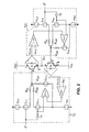
- FIG. 2 shows a circuit diagram of driver circuits according to an embodiment.
- high-side and low-side driver circuits 10, 20 are illustrated in more detail according to an embodiment. It should be noted that Figure 2 merely shows an example of one possible implementation of the driver circuits 10, 20.
- the high-side driver circuit 10 inputs are the duty ratio d and the collector-to-emitter voltage u ce,S2 of the second semiconductor switch S 2 .
- the low-side driver circuit 20 inputs are the complementary duty ratio d' and the collector-to-emitter voltage u ce,S1 of the first switch S 2 .
- V cc1 and V ee1 are supply voltages for the driver circuit 10 of the first semiconductor switch S 1 and are referenced to the emitter e of the first semiconductor switch S 1 .
- V cc2 and V ee2 are supply voltages for the driver circuit of the second semiconductor switch S 2 and are referenced to the emitter e of the second semiconductor switch S 2 .
- Resistances R off1 and R off2 are turn-off resistances and resistance R on is a turn-on resistance.
- the duty ratio signal d goes off, i.e. switch S on1 goes off and switch S off1a and switch S off1b go on (because of logic inverter Q 1 ) and the total turn-off gate resistance is a parallel connection of resistances R off1 and R off2 .
- u ce,S1 begins to rise toward u dc and u ce,S2 to descend toward 0 V.
- the rate of change of a voltage du/dt is dependent on the turn-off gate resistance, i.e. the lower the resistance is, the faster the voltage changes.
- the collector current of the first semiconductor switch S 1 starts to descend toward 0 A with a rate-of-change di/dt dependent on the turn-off gate resistance, i.e. the lower the gate resistance is, the faster the current changes.
- the turn-off gate resistance is changed at the point where the current starts to descend.
- the change of the value of the turn-off gate resistance of the first semiconductor switch S 1 may be implemented in such a way that, when u ce,S2 descends below the voltage threshold u th1 , comparator (CMP) output drops, and consequently the output of the AND gate also drops, and switch S off1b goes off. Thereafter, the total turn-off gate resistance is R off2 . Now di/dt is dependent on resistance R off2 , not the parallel connection of resistances R off2 and R oof1 , which has a lower resistance than resistance R off2 alone.
- Resistance R off1 preferably has a low value such that the voltage rise is fast, and resistance R off2 preferably has a higher value such that the current drop rate is limited to limit the voltage overshoot.
- the particular values for resistances R off2 and R off1 depend on the used semiconductor components, for instance. Therefore, no specific resistance values are given here.
- the voltage threshold u th1 may be ideally 0 V (if circuit operations are infinitely fast). In practice, the voltage threshold may be a relatively small positive value below the normal dc-link voltage u dc in order to compensate for delays in the circuit. With the circuit shown in Figure 2 , the voltage rise is fast but still the current drop rate is limited in turn-off instants, which results in a relatively low voltage overshoot but only slightly increased turn-off switching losses.
- the complementary duty ratio signal d' goes off, i.e. switch S on2 goes off and switch S off2a and switch S off2b go on (because of logic inverter Q 2 ) and the total turn-off gate resistance is a parallel connection of resistances R off1 and R off2 .
- u ce,S2 begins to rise toward u dc and u ce,S1 descends toward 0 V.
- the collector current of the second semiconductor switch S 2 starts to descend toward 0 A with a rate-of-change di/dt dependent on the turn-off gate resistance.
- the turn-off gate resistance is changed at the point where the current starts to descend.
- the change of the value of the turn-off gate resistance of the second semiconductor switch S 2 may be implemented in such a way that, when u ce,S1 descends below the voltage threshold u th2 , comparator (CMP) output drops, and consequently the output of the AND gate also drops, and switch S off2b goes off. Thereafter, the total turn-off gate resistance is R off2 .
- Resistance R off2 preferably has a low value such that the voltage rise is fast and resistance R off2 preferably has a higher value such that the current drop rate is limited to limit the voltage overshoot.
- the particular values for resistances R off2 and R off1 depend on the used semiconductor components, for instance. Therefore, no specific resistance values are given here.
- the voltage threshold u th2 may be ideally 0 V (if circuit operations are infinitely fast). In practice, the voltage threshold may be a relatively small positive value below the normal dc-link voltage u dc in order to compensate for delays in the circuit.
- Figure 3 shows a simulated collector-to-emitter voltage of an IGBT during a turn-off process according to an embodiment.
- the solid line shows the collector-to-emitter voltage of the IGBT during the turn-off process when the total turn-off gate resistance R g is changed from 3.3 ⁇ to 47 ⁇ during the turn-off process using a circuit corresponding to that of Figure 2 , for example.
- the dashed line shows the collector-to-emitter voltage of the IGBT during the turn-off process when the total turn-off gate resistance is kept constant at 3.3 ⁇ and the semi-dashed line shows the collector-to-emitter voltage of the IGBT during the turn-off process when the total turn-off gate resistance is kept constant at 47 ⁇ .
- Figure 4 shows a simulated gate-to-emitter voltage of an IGBT during a turn-off process according to an embodiment.
- the solid line shows the gate-to-emitter voltage of the IGBT during the turn-off process when the total turn-off gate resistance R g is changed from 3.3 ⁇ to 47 ⁇ during the turn-off process using a circuit corresponding to that of Figure 2 , for example.
- the dashed line shows the gate-to-emitter voltage of the IGBT during the turn-off process when the total turn-off gate resistance is kept constant at 3.3 ⁇
- the semi-dashed line shows the gate-to-emitter voltage of the IGBT during the turn-off process when the total turn-off gate resistance is kept constant at 47 ⁇ .
- the semi-dashed line shows the effect of a low gate discharge current on the switching speed. The whole turn-off instant is significantly longer than with the other two drivers, which increases the turn-off losses among other negative side effects (decreased practical switching frequency, control-system operation etc.).
- the switching time of the variable resistance driver circuit (solid line) is slightly longer than with the low turn-off resistance (dashed line), which is a necessity if the rate-of-change of current is decreased.
- the change of the gate resistance is shown as a peak in the solid line at approximately 100.2 ⁇ s, and thereafter the solid and dashed lines have a similar behavior.
- the simulated turn-off losses and voltage-peaking properties of the three driver circuits with different total turn-off gate resistances are collected into following Table 1.
- the variable resistance driver circuit has the best sides of low and high turn-off resistances; the turn-off losses are nearly as small as with the low turn-off resistance but the voltage peaking is significantly reduced.
- the comparator CMP in the circuit of Figure 2 could be tuned to trigger to a certain threshold voltage over the switch turned off.
- the gate resistance is changed only if the turn-off transient voltage exceeds a pre-specified safe limit, i.e. 1000 V in the case of 1200 V IGBT, for example.
- the driver circuit 10, 20 or a corresponding control arrangement driving the controllable semiconductor switches according to any one of the above embodiments, or a combination thereof can be implemented as one unit or as two or more separate units that are configured to implement the functionality of the various embodiments.
- the term 'unit' refers generally to a physical or logical entity, such as a physical device or a part thereof or a software routine.
- the driver circuit 10, 20 or a corresponding control arrangement according to any one of the embodiments may be implemented at least partly by means of one or more computers or corresponding digital signal processing (DSP) equipment provided with suitable software, for example.
- DSP digital signal processing
- Such a computer or digital signal processing equipment preferably comprises at least a working memory (RAM) providing a storage area for arithmetical operations, and a central processing unit (CPU), such as a general-purpose digital signal processor.
- the CPU may comprise a set of registers, an arithmetic logic unit, and a CPU control unit.
- the CPU control unit is controlled by a sequence of program instructions transferred to the CPU from the RAM.
- the CPU control unit may contain a number of microinstructions for basic operations. The implementation of microinstructions may vary depending on the CPU design.
- the program instructions may be coded by a programming language, which may be a high-level programming language, such as C, Java, etc., or a low-level programming language, such as a machine language, or an assembler.
- the computer may also have an operating system which may provide system services to a computer program written with the program instructions.
- the computer or other apparatus implementing the invention, or a part thereof, may further comprise suitable input means for receiving e.g. measurement and/or control data, and output means for outputting e.g. control data. It is also possible to use analog circuits, programmable logic devices (PLD), such as a field-programmable gate array (FPGA), or discrete electric components and devices for implementing the functionality according to any one of the embodiments.
- PLD programmable logic devices
- FPGA field-programmable gate array
- the driver circuit 10, 20 or a corresponding control arrangement according to any one of the embodiments may be implemented at least partly by means of such analog circuits or programmable logic devices, such as an FPGA circuit.
- An FPGA circuit or another type of a programmable logic device, for example, may be used to implement the logical functions according to any one of the embodiments.
- the invention can be implemented in existing system elements or by using separate dedicated elements or devices in a centralized or distributed manner.
- Present converters can comprise programmable logic devices, such as FPGA circuits, or processors and memory that can be utilized in the functions according to embodiments of the invention.
- all modifications and configurations required for implementing an embodiment of the invention e.g. in existing converters may be performed as software routines, which may be implemented as added or updated software routines.
- software can be provided as a computer program product comprising computer program code which, when run on a computer, causes the computer or a corresponding arrangement to perform the functionality according to the invention as described above.
- Such a computer program code may be stored or generally embodied on a computer readable medium, such as a suitable memory, e.g. a flash memory or an optical memory, from which it is loadable to the unit or units executing the program code.
- a computer program code implementing the invention may be loaded to the unit or units executing the computer program code via a suitable data network, for example, and it may replace or update a possibly existing program code.
Landscapes
- Power Conversion In General (AREA)
Priority Applications (1)
| Application Number | Priority Date | Filing Date | Title |
|---|---|---|---|
| EP13170414.0A EP2811648B1 (de) | 2013-06-04 | 2013-06-04 | Verfahren und Anordnung zur Steuerung eines Halbleiterschalters |
Applications Claiming Priority (1)
| Application Number | Priority Date | Filing Date | Title |
|---|---|---|---|
| EP13170414.0A EP2811648B1 (de) | 2013-06-04 | 2013-06-04 | Verfahren und Anordnung zur Steuerung eines Halbleiterschalters |
Publications (2)
| Publication Number | Publication Date |
|---|---|
| EP2811648A1 true EP2811648A1 (de) | 2014-12-10 |
| EP2811648B1 EP2811648B1 (de) | 2015-12-02 |
Family
ID=48536751
Family Applications (1)
| Application Number | Title | Priority Date | Filing Date |
|---|---|---|---|
| EP13170414.0A Active EP2811648B1 (de) | 2013-06-04 | 2013-06-04 | Verfahren und Anordnung zur Steuerung eines Halbleiterschalters |
Country Status (1)
| Country | Link |
|---|---|
| EP (1) | EP2811648B1 (de) |
Cited By (2)
| Publication number | Priority date | Publication date | Assignee | Title |
|---|---|---|---|---|
| EP3051697A1 (de) * | 2015-01-30 | 2016-08-03 | Delta Electronics, Inc. | Treiberschaltung für einen halbleiterschalter |
| WO2021175496A1 (en) * | 2020-03-06 | 2021-09-10 | Eaton Intelligent Power Limited | Active gate driver for wide band gap power semiconductor devices |
Citations (3)
| Publication number | Priority date | Publication date | Assignee | Title |
|---|---|---|---|---|
| US5926012A (en) * | 1996-09-20 | 1999-07-20 | Fuji Electric Co., Ltd. | Gate drive circuit in power converter with condition detection device |
| US20110273206A1 (en) * | 2010-05-06 | 2011-11-10 | Lsis Co., Ltd. | Switching gate driver |
| US20130107584A1 (en) * | 2011-11-01 | 2013-05-02 | Iwatt, Inc. | Dynamic Mosfet Gate Drivers |
-
2013
- 2013-06-04 EP EP13170414.0A patent/EP2811648B1/de active Active
Patent Citations (3)
| Publication number | Priority date | Publication date | Assignee | Title |
|---|---|---|---|---|
| US5926012A (en) * | 1996-09-20 | 1999-07-20 | Fuji Electric Co., Ltd. | Gate drive circuit in power converter with condition detection device |
| US20110273206A1 (en) * | 2010-05-06 | 2011-11-10 | Lsis Co., Ltd. | Switching gate driver |
| US20130107584A1 (en) * | 2011-11-01 | 2013-05-02 | Iwatt, Inc. | Dynamic Mosfet Gate Drivers |
Cited By (7)
| Publication number | Priority date | Publication date | Assignee | Title |
|---|---|---|---|---|
| EP3051697A1 (de) * | 2015-01-30 | 2016-08-03 | Delta Electronics, Inc. | Treiberschaltung für einen halbleiterschalter |
| JP2016144388A (ja) * | 2015-01-30 | 2016-08-08 | 台▲達▼▲電▼子工▲業▼股▲ふん▼有限公司 | コンバータシステム、半導体スイッチ駆動回路及び半導体スイッチ駆動方法 |
| CN105991004A (zh) * | 2015-01-30 | 2016-10-05 | 台达电子工业股份有限公司 | 变换器系统、半导体开关驱动电路及方法 |
| US10128832B2 (en) | 2015-01-30 | 2018-11-13 | Delta Electronics, Inc. | Converter system, driving circuit and method for semiconductor switch |
| CN105991004B (zh) * | 2015-01-30 | 2019-06-11 | 台达电子工业股份有限公司 | 变换器系统、半导体开关驱动电路及方法 |
| WO2021175496A1 (en) * | 2020-03-06 | 2021-09-10 | Eaton Intelligent Power Limited | Active gate driver for wide band gap power semiconductor devices |
| US12231033B2 (en) | 2020-03-06 | 2025-02-18 | Eaton Intelligent Power Limited | Active gate driver for wide band gap power semiconductor devices |
Also Published As
| Publication number | Publication date |
|---|---|
| EP2811648B1 (de) | 2015-12-02 |
Similar Documents
| Publication | Publication Date | Title |
|---|---|---|
| US9954521B2 (en) | Gate drive circuit for semiconductor switching devices | |
| JP6362996B2 (ja) | 半導体駆動装置ならびにそれを用いた電力変換装置 | |
| US8723589B2 (en) | Switching device with a cascode circuit | |
| JP4512671B1 (ja) | 電力変換回路 | |
| CN102859858A (zh) | 电力变换装置 | |
| HK1232343A1 (zh) | 控制电子开关的集电极到发射极电压变化的栅极驱动器以及包括所述栅极驱动器的电路 | |
| JP5344005B2 (ja) | スイッチング回路 | |
| CN101335483A (zh) | 电力变换装置 | |
| JP2003069401A (ja) | 半導体電力変換装置 | |
| US11621709B2 (en) | Power module with built-in drive circuits | |
| CN105453434A (zh) | 采用氮化镓开关的驱动单元 | |
| WO2015111154A1 (ja) | スイッチング回路、インバータ回路、及びモータ制御装置 | |
| JP6725328B2 (ja) | ゲート駆動回路 | |
| EP2811648B1 (de) | Verfahren und Anordnung zur Steuerung eines Halbleiterschalters | |
| US12119817B2 (en) | Gate driver circuits with independently tunable performance characteristics | |
| US12368435B2 (en) | Gate drive circuit | |
| CN118077128A (zh) | 电力用半导体元件的驱动电路、电力用半导体模块以及电力变换装置 | |
| JP5843535B2 (ja) | 半導体モジュール | |
| JP2019154134A (ja) | ゲート駆動装置 | |
| CN120049723A (zh) | 栅极驱动器电路、检测短路的方法以及计算机可读介质 | |
| JP4971603B2 (ja) | 電圧駆動型半導体スイッチング素子の駆動方法 | |
| JP6288220B2 (ja) | 電圧駆動型半導体素子の駆動回路 | |
| JPH10209832A (ja) | 半導体スイッチ回路 | |
| JP2022143030A (ja) | 駆動回路、半導体装置 | |
| US20160336883A1 (en) | Semiconductor device and motor driving method |
Legal Events
| Date | Code | Title | Description |
|---|---|---|---|
| PUAI | Public reference made under article 153(3) epc to a published international application that has entered the european phase |
Free format text: ORIGINAL CODE: 0009012 |
|
| 17P | Request for examination filed |
Effective date: 20131116 |
|
| AK | Designated contracting states |
Kind code of ref document: A1 Designated state(s): AL AT BE BG CH CY CZ DE DK EE ES FI FR GB GR HR HU IE IS IT LI LT LU LV MC MK MT NL NO PL PT RO RS SE SI SK SM TR |
|
| AX | Request for extension of the european patent |
Extension state: BA ME |
|
| GRAP | Despatch of communication of intention to grant a patent |
Free format text: ORIGINAL CODE: EPIDOSNIGR1 |
|
| INTG | Intention to grant announced |
Effective date: 20150618 |
|
| GRAS | Grant fee paid |
Free format text: ORIGINAL CODE: EPIDOSNIGR3 |
|
| GRAA | (expected) grant |
Free format text: ORIGINAL CODE: 0009210 |
|
| AK | Designated contracting states |
Kind code of ref document: B1 Designated state(s): AL AT BE BG CH CY CZ DE DK EE ES FI FR GB GR HR HU IE IS IT LI LT LU LV MC MK MT NL NO PL PT RO RS SE SI SK SM TR |
|
| REG | Reference to a national code |
Ref country code: GB Ref legal event code: FG4D |
|
| REG | Reference to a national code |
Ref country code: AT Ref legal event code: REF Ref document number: 764022 Country of ref document: AT Kind code of ref document: T Effective date: 20151215 Ref country code: CH Ref legal event code: EP |
|
| REG | Reference to a national code |
Ref country code: IE Ref legal event code: FG4D |
|
| REG | Reference to a national code |
Ref country code: DE Ref legal event code: R096 Ref document number: 602013003962 Country of ref document: DE |
|
| RAP2 | Party data changed (patent owner data changed or rights of a patent transferred) |
Owner name: ABB TECHNOLOGY OY |
|
| REG | Reference to a national code |
Ref country code: NL Ref legal event code: MP Effective date: 20160302 |
|
| REG | Reference to a national code |
Ref country code: LT Ref legal event code: MG4D |
|
| REG | Reference to a national code |
Ref country code: GB Ref legal event code: 732E Free format text: REGISTERED BETWEEN 20160317 AND 20160323 |
|
| REG | Reference to a national code |
Ref country code: AT Ref legal event code: MK05 Ref document number: 764022 Country of ref document: AT Kind code of ref document: T Effective date: 20151202 |
|
| REG | Reference to a national code |
Ref country code: DE Ref legal event code: R081 Ref document number: 602013003962 Country of ref document: DE Owner name: ABB TECHNOLOGY OY, FI Free format text: FORMER OWNER: ABB OY, HELSINKI, FI Ref country code: DE Ref legal event code: R081 Ref document number: 602013003962 Country of ref document: DE Owner name: ABB SCHWEIZ AG, CH Free format text: FORMER OWNER: ABB OY, HELSINKI, FI |
|
| PG25 | Lapsed in a contracting state [announced via postgrant information from national office to epo] |
Ref country code: HR Free format text: LAPSE BECAUSE OF FAILURE TO SUBMIT A TRANSLATION OF THE DESCRIPTION OR TO PAY THE FEE WITHIN THE PRESCRIBED TIME-LIMIT Effective date: 20151202 Ref country code: ES Free format text: LAPSE BECAUSE OF FAILURE TO SUBMIT A TRANSLATION OF THE DESCRIPTION OR TO PAY THE FEE WITHIN THE PRESCRIBED TIME-LIMIT Effective date: 20151202 Ref country code: NO Free format text: LAPSE BECAUSE OF FAILURE TO SUBMIT A TRANSLATION OF THE DESCRIPTION OR TO PAY THE FEE WITHIN THE PRESCRIBED TIME-LIMIT Effective date: 20160302 Ref country code: LT Free format text: LAPSE BECAUSE OF FAILURE TO SUBMIT A TRANSLATION OF THE DESCRIPTION OR TO PAY THE FEE WITHIN THE PRESCRIBED TIME-LIMIT Effective date: 20151202 |
|
| REG | Reference to a national code |
Ref country code: DE Ref legal event code: R082 Ref document number: 602013003962 Country of ref document: DE |
|
| PG25 | Lapsed in a contracting state [announced via postgrant information from national office to epo] |
Ref country code: NL Free format text: LAPSE BECAUSE OF FAILURE TO SUBMIT A TRANSLATION OF THE DESCRIPTION OR TO PAY THE FEE WITHIN THE PRESCRIBED TIME-LIMIT Effective date: 20151202 Ref country code: SE Free format text: LAPSE BECAUSE OF FAILURE TO SUBMIT A TRANSLATION OF THE DESCRIPTION OR TO PAY THE FEE WITHIN THE PRESCRIBED TIME-LIMIT Effective date: 20151202 Ref country code: RS Free format text: LAPSE BECAUSE OF FAILURE TO SUBMIT A TRANSLATION OF THE DESCRIPTION OR TO PAY THE FEE WITHIN THE PRESCRIBED TIME-LIMIT Effective date: 20151202 Ref country code: AT Free format text: LAPSE BECAUSE OF FAILURE TO SUBMIT A TRANSLATION OF THE DESCRIPTION OR TO PAY THE FEE WITHIN THE PRESCRIBED TIME-LIMIT Effective date: 20151202 Ref country code: LV Free format text: LAPSE BECAUSE OF FAILURE TO SUBMIT A TRANSLATION OF THE DESCRIPTION OR TO PAY THE FEE WITHIN THE PRESCRIBED TIME-LIMIT Effective date: 20151202 Ref country code: GR Free format text: LAPSE BECAUSE OF FAILURE TO SUBMIT A TRANSLATION OF THE DESCRIPTION OR TO PAY THE FEE WITHIN THE PRESCRIBED TIME-LIMIT Effective date: 20160303 Ref country code: PL Free format text: LAPSE BECAUSE OF FAILURE TO SUBMIT A TRANSLATION OF THE DESCRIPTION OR TO PAY THE FEE WITHIN THE PRESCRIBED TIME-LIMIT Effective date: 20151202 |
|
| REG | Reference to a national code |
Ref country code: FR Ref legal event code: PLFP Year of fee payment: 4 |
|
| PG25 | Lapsed in a contracting state [announced via postgrant information from national office to epo] |
Ref country code: IS Free format text: LAPSE BECAUSE OF FAILURE TO SUBMIT A TRANSLATION OF THE DESCRIPTION OR TO PAY THE FEE WITHIN THE PRESCRIBED TIME-LIMIT Effective date: 20151202 |
|
| PG25 | Lapsed in a contracting state [announced via postgrant information from national office to epo] |
Ref country code: CZ Free format text: LAPSE BECAUSE OF FAILURE TO SUBMIT A TRANSLATION OF THE DESCRIPTION OR TO PAY THE FEE WITHIN THE PRESCRIBED TIME-LIMIT Effective date: 20151202 |
|
| PG25 | Lapsed in a contracting state [announced via postgrant information from national office to epo] |
Ref country code: SM Free format text: LAPSE BECAUSE OF FAILURE TO SUBMIT A TRANSLATION OF THE DESCRIPTION OR TO PAY THE FEE WITHIN THE PRESCRIBED TIME-LIMIT Effective date: 20151202 Ref country code: SK Free format text: LAPSE BECAUSE OF FAILURE TO SUBMIT A TRANSLATION OF THE DESCRIPTION OR TO PAY THE FEE WITHIN THE PRESCRIBED TIME-LIMIT Effective date: 20151202 Ref country code: RO Free format text: LAPSE BECAUSE OF FAILURE TO SUBMIT A TRANSLATION OF THE DESCRIPTION OR TO PAY THE FEE WITHIN THE PRESCRIBED TIME-LIMIT Effective date: 20151202 Ref country code: PT Free format text: LAPSE BECAUSE OF FAILURE TO SUBMIT A TRANSLATION OF THE DESCRIPTION OR TO PAY THE FEE WITHIN THE PRESCRIBED TIME-LIMIT Effective date: 20160404 Ref country code: IS Free format text: LAPSE BECAUSE OF FAILURE TO SUBMIT A TRANSLATION OF THE DESCRIPTION OR TO PAY THE FEE WITHIN THE PRESCRIBED TIME-LIMIT Effective date: 20160402 Ref country code: EE Free format text: LAPSE BECAUSE OF FAILURE TO SUBMIT A TRANSLATION OF THE DESCRIPTION OR TO PAY THE FEE WITHIN THE PRESCRIBED TIME-LIMIT Effective date: 20151202 |
|
| REG | Reference to a national code |
Ref country code: DE Ref legal event code: R097 Ref document number: 602013003962 Country of ref document: DE |
|
| PLBE | No opposition filed within time limit |
Free format text: ORIGINAL CODE: 0009261 |
|
| STAA | Information on the status of an ep patent application or granted ep patent |
Free format text: STATUS: NO OPPOSITION FILED WITHIN TIME LIMIT |
|
| PG25 | Lapsed in a contracting state [announced via postgrant information from national office to epo] |
Ref country code: DK Free format text: LAPSE BECAUSE OF FAILURE TO SUBMIT A TRANSLATION OF THE DESCRIPTION OR TO PAY THE FEE WITHIN THE PRESCRIBED TIME-LIMIT Effective date: 20151202 |
|
| 26N | No opposition filed |
Effective date: 20160905 |
|
| PG25 | Lapsed in a contracting state [announced via postgrant information from national office to epo] |
Ref country code: SI Free format text: LAPSE BECAUSE OF FAILURE TO SUBMIT A TRANSLATION OF THE DESCRIPTION OR TO PAY THE FEE WITHIN THE PRESCRIBED TIME-LIMIT Effective date: 20151202 |
|
| PG25 | Lapsed in a contracting state [announced via postgrant information from national office to epo] |
Ref country code: BE Free format text: LAPSE BECAUSE OF FAILURE TO SUBMIT A TRANSLATION OF THE DESCRIPTION OR TO PAY THE FEE WITHIN THE PRESCRIBED TIME-LIMIT Effective date: 20151202 |
|
| PG25 | Lapsed in a contracting state [announced via postgrant information from national office to epo] |
Ref country code: MC Free format text: LAPSE BECAUSE OF FAILURE TO SUBMIT A TRANSLATION OF THE DESCRIPTION OR TO PAY THE FEE WITHIN THE PRESCRIBED TIME-LIMIT Effective date: 20151202 |
|
| REG | Reference to a national code |
Ref country code: CH Ref legal event code: PL |
|
| REG | Reference to a national code |
Ref country code: IE Ref legal event code: MM4A |
|
| PG25 | Lapsed in a contracting state [announced via postgrant information from national office to epo] |
Ref country code: LI Free format text: LAPSE BECAUSE OF NON-PAYMENT OF DUE FEES Effective date: 20160630 Ref country code: CH Free format text: LAPSE BECAUSE OF NON-PAYMENT OF DUE FEES Effective date: 20160630 |
|
| PG25 | Lapsed in a contracting state [announced via postgrant information from national office to epo] |
Ref country code: IE Free format text: LAPSE BECAUSE OF NON-PAYMENT OF DUE FEES Effective date: 20160604 |
|
| REG | Reference to a national code |
Ref country code: FR Ref legal event code: PLFP Year of fee payment: 5 |
|
| PG25 | Lapsed in a contracting state [announced via postgrant information from national office to epo] |
Ref country code: HU Free format text: LAPSE BECAUSE OF FAILURE TO SUBMIT A TRANSLATION OF THE DESCRIPTION OR TO PAY THE FEE WITHIN THE PRESCRIBED TIME-LIMIT; INVALID AB INITIO Effective date: 20130604 |
|
| REG | Reference to a national code |
Ref country code: FR Ref legal event code: PLFP Year of fee payment: 6 |
|
| PG25 | Lapsed in a contracting state [announced via postgrant information from national office to epo] |
Ref country code: LU Free format text: LAPSE BECAUSE OF NON-PAYMENT OF DUE FEES Effective date: 20160604 Ref country code: CY Free format text: LAPSE BECAUSE OF FAILURE TO SUBMIT A TRANSLATION OF THE DESCRIPTION OR TO PAY THE FEE WITHIN THE PRESCRIBED TIME-LIMIT Effective date: 20151202 Ref country code: MK Free format text: LAPSE BECAUSE OF FAILURE TO SUBMIT A TRANSLATION OF THE DESCRIPTION OR TO PAY THE FEE WITHIN THE PRESCRIBED TIME-LIMIT Effective date: 20151202 Ref country code: MT Free format text: LAPSE BECAUSE OF NON-PAYMENT OF DUE FEES Effective date: 20160630 |
|
| PG25 | Lapsed in a contracting state [announced via postgrant information from national office to epo] |
Ref country code: BG Free format text: LAPSE BECAUSE OF FAILURE TO SUBMIT A TRANSLATION OF THE DESCRIPTION OR TO PAY THE FEE WITHIN THE PRESCRIBED TIME-LIMIT Effective date: 20151202 |
|
| REG | Reference to a national code |
Ref country code: DE Ref legal event code: R081 Ref document number: 602013003962 Country of ref document: DE Owner name: ABB SCHWEIZ AG, CH Free format text: FORMER OWNER: ABB TECHNOLOGY OY, HELSINKI, FI |
|
| PG25 | Lapsed in a contracting state [announced via postgrant information from national office to epo] |
Ref country code: TR Free format text: LAPSE BECAUSE OF FAILURE TO SUBMIT A TRANSLATION OF THE DESCRIPTION OR TO PAY THE FEE WITHIN THE PRESCRIBED TIME-LIMIT Effective date: 20151202 Ref country code: AL Free format text: LAPSE BECAUSE OF FAILURE TO SUBMIT A TRANSLATION OF THE DESCRIPTION OR TO PAY THE FEE WITHIN THE PRESCRIBED TIME-LIMIT Effective date: 20151202 |
|
| REG | Reference to a national code |
Ref country code: GB Ref legal event code: 732E Free format text: REGISTERED BETWEEN 20181025 AND 20181102 |
|
| PGFP | Annual fee paid to national office [announced via postgrant information from national office to epo] |
Ref country code: FI Payment date: 20250627 Year of fee payment: 13 |
|
| PGFP | Annual fee paid to national office [announced via postgrant information from national office to epo] |
Ref country code: DE Payment date: 20250618 Year of fee payment: 13 |
|
| PGFP | Annual fee paid to national office [announced via postgrant information from national office to epo] |
Ref country code: GB Payment date: 20250618 Year of fee payment: 13 |
|
| PGFP | Annual fee paid to national office [announced via postgrant information from national office to epo] |
Ref country code: FR Payment date: 20250624 Year of fee payment: 13 |
|
| PGFP | Annual fee paid to national office [announced via postgrant information from national office to epo] |
Ref country code: IT Payment date: 20250624 Year of fee payment: 13 |