EP2811482B1 - Appareil d'affichage tactile à cristaux liquides - Google Patents
Appareil d'affichage tactile à cristaux liquides Download PDFInfo
- Publication number
- EP2811482B1 EP2811482B1 EP14152427.2A EP14152427A EP2811482B1 EP 2811482 B1 EP2811482 B1 EP 2811482B1 EP 14152427 A EP14152427 A EP 14152427A EP 2811482 B1 EP2811482 B1 EP 2811482B1
- Authority
- EP
- European Patent Office
- Prior art keywords
- touch
- control circuit
- display
- touch control
- common electrodes
- Prior art date
- Legal status (The legal status is an assumption and is not a legal conclusion. Google has not performed a legal analysis and makes no representation as to the accuracy of the status listed.)
- Active
Links
- 239000004973 liquid crystal related substance Substances 0.000 title claims description 16
- 239000000758 substrate Substances 0.000 claims description 30
- 239000010409 thin film Substances 0.000 claims description 17
- AMGQUBHHOARCQH-UHFFFAOYSA-N indium;oxotin Chemical compound [In].[Sn]=O AMGQUBHHOARCQH-UHFFFAOYSA-N 0.000 claims description 12
- 239000000463 material Substances 0.000 claims description 12
- 230000004044 response Effects 0.000 claims description 10
- 239000011159 matrix material Substances 0.000 claims description 8
- 239000011521 glass Substances 0.000 claims description 5
- 230000005684 electric field Effects 0.000 claims description 3
- 238000000034 method Methods 0.000 claims description 3
- 230000004907 flux Effects 0.000 claims description 2
- 229910044991 metal oxide Inorganic materials 0.000 description 9
- 150000004706 metal oxides Chemical class 0.000 description 9
- OKTJSMMVPCPJKN-UHFFFAOYSA-N Carbon Chemical compound [C] OKTJSMMVPCPJKN-UHFFFAOYSA-N 0.000 description 8
- 238000004891 communication Methods 0.000 description 8
- 229910021389 graphene Inorganic materials 0.000 description 8
- 238000001514 detection method Methods 0.000 description 7
- 229910052751 metal Inorganic materials 0.000 description 7
- 239000002184 metal Substances 0.000 description 7
- 238000004519 manufacturing process Methods 0.000 description 4
- 229910003460 diamond Inorganic materials 0.000 description 3
- 239000010432 diamond Substances 0.000 description 3
- 230000008859 change Effects 0.000 description 2
- 238000005530 etching Methods 0.000 description 2
- 230000003287 optical effect Effects 0.000 description 2
- 238000009825 accumulation Methods 0.000 description 1
- 239000003990 capacitor Substances 0.000 description 1
- 239000004020 conductor Substances 0.000 description 1
- 230000000694 effects Effects 0.000 description 1
- 238000005516 engineering process Methods 0.000 description 1
- 230000008569 process Effects 0.000 description 1
- 230000000750 progressive effect Effects 0.000 description 1
- 230000035945 sensitivity Effects 0.000 description 1
- 230000001360 synchronised effect Effects 0.000 description 1
Images


Classifications
-
- G—PHYSICS
- G06—COMPUTING; CALCULATING OR COUNTING
- G06F—ELECTRIC DIGITAL DATA PROCESSING
- G06F3/00—Input arrangements for transferring data to be processed into a form capable of being handled by the computer; Output arrangements for transferring data from processing unit to output unit, e.g. interface arrangements
- G06F3/01—Input arrangements or combined input and output arrangements for interaction between user and computer
- G06F3/03—Arrangements for converting the position or the displacement of a member into a coded form
- G06F3/041—Digitisers, e.g. for touch screens or touch pads, characterised by the transducing means
- G06F3/044—Digitisers, e.g. for touch screens or touch pads, characterised by the transducing means by capacitive means
- G06F3/0443—Digitisers, e.g. for touch screens or touch pads, characterised by the transducing means by capacitive means using a single layer of sensing electrodes
-
- G—PHYSICS
- G06—COMPUTING; CALCULATING OR COUNTING
- G06F—ELECTRIC DIGITAL DATA PROCESSING
- G06F3/00—Input arrangements for transferring data to be processed into a form capable of being handled by the computer; Output arrangements for transferring data from processing unit to output unit, e.g. interface arrangements
- G06F3/01—Input arrangements or combined input and output arrangements for interaction between user and computer
- G06F3/03—Arrangements for converting the position or the displacement of a member into a coded form
- G06F3/041—Digitisers, e.g. for touch screens or touch pads, characterised by the transducing means
- G06F3/0412—Digitisers structurally integrated in a display
-
- G—PHYSICS
- G02—OPTICS
- G02F—OPTICAL DEVICES OR ARRANGEMENTS FOR THE CONTROL OF LIGHT BY MODIFICATION OF THE OPTICAL PROPERTIES OF THE MEDIA OF THE ELEMENTS INVOLVED THEREIN; NON-LINEAR OPTICS; FREQUENCY-CHANGING OF LIGHT; OPTICAL LOGIC ELEMENTS; OPTICAL ANALOGUE/DIGITAL CONVERTERS
- G02F1/00—Devices or arrangements for the control of the intensity, colour, phase, polarisation or direction of light arriving from an independent light source, e.g. switching, gating or modulating; Non-linear optics
- G02F1/01—Devices or arrangements for the control of the intensity, colour, phase, polarisation or direction of light arriving from an independent light source, e.g. switching, gating or modulating; Non-linear optics for the control of the intensity, phase, polarisation or colour
- G02F1/13—Devices or arrangements for the control of the intensity, colour, phase, polarisation or direction of light arriving from an independent light source, e.g. switching, gating or modulating; Non-linear optics for the control of the intensity, phase, polarisation or colour based on liquid crystals, e.g. single liquid crystal display cells
- G02F1/133—Constructional arrangements; Operation of liquid crystal cells; Circuit arrangements
- G02F1/1333—Constructional arrangements; Manufacturing methods
- G02F1/13338—Input devices, e.g. touch panels
-
- G—PHYSICS
- G02—OPTICS
- G02F—OPTICAL DEVICES OR ARRANGEMENTS FOR THE CONTROL OF LIGHT BY MODIFICATION OF THE OPTICAL PROPERTIES OF THE MEDIA OF THE ELEMENTS INVOLVED THEREIN; NON-LINEAR OPTICS; FREQUENCY-CHANGING OF LIGHT; OPTICAL LOGIC ELEMENTS; OPTICAL ANALOGUE/DIGITAL CONVERTERS
- G02F1/00—Devices or arrangements for the control of the intensity, colour, phase, polarisation or direction of light arriving from an independent light source, e.g. switching, gating or modulating; Non-linear optics
- G02F1/01—Devices or arrangements for the control of the intensity, colour, phase, polarisation or direction of light arriving from an independent light source, e.g. switching, gating or modulating; Non-linear optics for the control of the intensity, phase, polarisation or colour
- G02F1/13—Devices or arrangements for the control of the intensity, colour, phase, polarisation or direction of light arriving from an independent light source, e.g. switching, gating or modulating; Non-linear optics for the control of the intensity, phase, polarisation or colour based on liquid crystals, e.g. single liquid crystal display cells
- G02F1/133—Constructional arrangements; Operation of liquid crystal cells; Circuit arrangements
- G02F1/1333—Constructional arrangements; Manufacturing methods
- G02F1/1343—Electrodes
- G02F1/134309—Electrodes characterised by their geometrical arrangement
-
- G—PHYSICS
- G06—COMPUTING; CALCULATING OR COUNTING
- G06F—ELECTRIC DIGITAL DATA PROCESSING
- G06F3/00—Input arrangements for transferring data to be processed into a form capable of being handled by the computer; Output arrangements for transferring data from processing unit to output unit, e.g. interface arrangements
- G06F3/01—Input arrangements or combined input and output arrangements for interaction between user and computer
- G06F3/03—Arrangements for converting the position or the displacement of a member into a coded form
- G06F3/041—Digitisers, e.g. for touch screens or touch pads, characterised by the transducing means
- G06F3/0416—Control or interface arrangements specially adapted for digitisers
- G06F3/04166—Details of scanning methods, e.g. sampling time, grouping of sub areas or time sharing with display driving
-
- G—PHYSICS
- G06—COMPUTING; CALCULATING OR COUNTING
- G06F—ELECTRIC DIGITAL DATA PROCESSING
- G06F3/00—Input arrangements for transferring data to be processed into a form capable of being handled by the computer; Output arrangements for transferring data from processing unit to output unit, e.g. interface arrangements
- G06F3/01—Input arrangements or combined input and output arrangements for interaction between user and computer
- G06F3/03—Arrangements for converting the position or the displacement of a member into a coded form
- G06F3/041—Digitisers, e.g. for touch screens or touch pads, characterised by the transducing means
- G06F3/0416—Control or interface arrangements specially adapted for digitisers
- G06F3/0418—Control or interface arrangements specially adapted for digitisers for error correction or compensation, e.g. based on parallax, calibration or alignment
- G06F3/04184—Synchronisation with the driving of the display or the backlighting unit to avoid interferences generated internally
-
- G—PHYSICS
- G06—COMPUTING; CALCULATING OR COUNTING
- G06F—ELECTRIC DIGITAL DATA PROCESSING
- G06F3/00—Input arrangements for transferring data to be processed into a form capable of being handled by the computer; Output arrangements for transferring data from processing unit to output unit, e.g. interface arrangements
- G06F3/01—Input arrangements or combined input and output arrangements for interaction between user and computer
- G06F3/03—Arrangements for converting the position or the displacement of a member into a coded form
- G06F3/041—Digitisers, e.g. for touch screens or touch pads, characterised by the transducing means
- G06F3/044—Digitisers, e.g. for touch screens or touch pads, characterised by the transducing means by capacitive means
- G06F3/0445—Digitisers, e.g. for touch screens or touch pads, characterised by the transducing means by capacitive means using two or more layers of sensing electrodes, e.g. using two layers of electrodes separated by a dielectric layer
-
- G—PHYSICS
- G06—COMPUTING; CALCULATING OR COUNTING
- G06F—ELECTRIC DIGITAL DATA PROCESSING
- G06F3/00—Input arrangements for transferring data to be processed into a form capable of being handled by the computer; Output arrangements for transferring data from processing unit to output unit, e.g. interface arrangements
- G06F3/01—Input arrangements or combined input and output arrangements for interaction between user and computer
- G06F3/03—Arrangements for converting the position or the displacement of a member into a coded form
- G06F3/041—Digitisers, e.g. for touch screens or touch pads, characterised by the transducing means
- G06F3/044—Digitisers, e.g. for touch screens or touch pads, characterised by the transducing means by capacitive means
- G06F3/0446—Digitisers, e.g. for touch screens or touch pads, characterised by the transducing means by capacitive means using a grid-like structure of electrodes in at least two directions, e.g. using row and column electrodes
-
- G—PHYSICS
- G09—EDUCATION; CRYPTOGRAPHY; DISPLAY; ADVERTISING; SEALS
- G09G—ARRANGEMENTS OR CIRCUITS FOR CONTROL OF INDICATING DEVICES USING STATIC MEANS TO PRESENT VARIABLE INFORMATION
- G09G3/00—Control arrangements or circuits, of interest only in connection with visual indicators other than cathode-ray tubes
- G09G3/20—Control arrangements or circuits, of interest only in connection with visual indicators other than cathode-ray tubes for presentation of an assembly of a number of characters, e.g. a page, by composing the assembly by combination of individual elements arranged in a matrix no fixed position being assigned to or needed to be assigned to the individual characters or partial characters
- G09G3/34—Control arrangements or circuits, of interest only in connection with visual indicators other than cathode-ray tubes for presentation of an assembly of a number of characters, e.g. a page, by composing the assembly by combination of individual elements arranged in a matrix no fixed position being assigned to or needed to be assigned to the individual characters or partial characters by control of light from an independent source
- G09G3/36—Control arrangements or circuits, of interest only in connection with visual indicators other than cathode-ray tubes for presentation of an assembly of a number of characters, e.g. a page, by composing the assembly by combination of individual elements arranged in a matrix no fixed position being assigned to or needed to be assigned to the individual characters or partial characters by control of light from an independent source using liquid crystals
-
- G—PHYSICS
- G02—OPTICS
- G02F—OPTICAL DEVICES OR ARRANGEMENTS FOR THE CONTROL OF LIGHT BY MODIFICATION OF THE OPTICAL PROPERTIES OF THE MEDIA OF THE ELEMENTS INVOLVED THEREIN; NON-LINEAR OPTICS; FREQUENCY-CHANGING OF LIGHT; OPTICAL LOGIC ELEMENTS; OPTICAL ANALOGUE/DIGITAL CONVERTERS
- G02F1/00—Devices or arrangements for the control of the intensity, colour, phase, polarisation or direction of light arriving from an independent light source, e.g. switching, gating or modulating; Non-linear optics
- G02F1/01—Devices or arrangements for the control of the intensity, colour, phase, polarisation or direction of light arriving from an independent light source, e.g. switching, gating or modulating; Non-linear optics for the control of the intensity, phase, polarisation or colour
- G02F1/13—Devices or arrangements for the control of the intensity, colour, phase, polarisation or direction of light arriving from an independent light source, e.g. switching, gating or modulating; Non-linear optics for the control of the intensity, phase, polarisation or colour based on liquid crystals, e.g. single liquid crystal display cells
- G02F1/133—Constructional arrangements; Operation of liquid crystal cells; Circuit arrangements
- G02F1/1333—Constructional arrangements; Manufacturing methods
- G02F1/1343—Electrodes
- G02F1/134309—Electrodes characterised by their geometrical arrangement
- G02F1/134363—Electrodes characterised by their geometrical arrangement for applying an electric field parallel to the substrate, i.e. in-plane switching [IPS]
-
- G—PHYSICS
- G02—OPTICS
- G02F—OPTICAL DEVICES OR ARRANGEMENTS FOR THE CONTROL OF LIGHT BY MODIFICATION OF THE OPTICAL PROPERTIES OF THE MEDIA OF THE ELEMENTS INVOLVED THEREIN; NON-LINEAR OPTICS; FREQUENCY-CHANGING OF LIGHT; OPTICAL LOGIC ELEMENTS; OPTICAL ANALOGUE/DIGITAL CONVERTERS
- G02F2201/00—Constructional arrangements not provided for in groups G02F1/00 - G02F7/00
- G02F2201/12—Constructional arrangements not provided for in groups G02F1/00 - G02F7/00 electrode
- G02F2201/121—Constructional arrangements not provided for in groups G02F1/00 - G02F7/00 electrode common or background
-
- G—PHYSICS
- G06—COMPUTING; CALCULATING OR COUNTING
- G06F—ELECTRIC DIGITAL DATA PROCESSING
- G06F3/00—Input arrangements for transferring data to be processed into a form capable of being handled by the computer; Output arrangements for transferring data from processing unit to output unit, e.g. interface arrangements
- G06F3/01—Input arrangements or combined input and output arrangements for interaction between user and computer
- G06F3/03—Arrangements for converting the position or the displacement of a member into a coded form
- G06F3/041—Digitisers, e.g. for touch screens or touch pads, characterised by the transducing means
- G06F3/0416—Control or interface arrangements specially adapted for digitisers
- G06F3/04164—Connections between sensors and controllers, e.g. routing lines between electrodes and connection pads
Definitions
- An integrated touch screen can include multi-function circuit elements that form part of the display circuitry of the display system that generates an image on the display, and also form part of the touch sensing circuitry of a touch sensing system that senses one or more touches on or near the display.
- the multi-function circuit elements can be, for example, capacitors in display pixels of an LCD that are configured to operate as display circuitry in the display system, and that may also be configured to operate as touch circuitry of the touch sensing system.
- one or more circuit elements of the display pixel stackup can form a conductive portion of the touch sensing system, such as a charge collector, which can be operated with switches and conductive lines to sense touch.
- a touch display apparatus is provided according to the embodiments of the present disclosure to solve at least one of the above-mentioned problems.
- the wires are disposed in a layer provided with the pixel electrodes, and are connected to the multiple common electrodes through via holes.
- the chip of the display control circuit and the chip of the touch control circuit are bound onto the first substrate or the second substrate in chip-on-glass mode.
- the touch control circuit is adapted to determine a touch position according to a two-dimensional capacitance sensing array.
- the display touch screen has an in-plane switching structure, a fringe field switching structure, or a twisted nematic structure.
- Concave and convex structure is provided at edges of the common electrode.
- the material of multiple common electrodes is metal oxide such as indium tin oxide or graphene.
- the touch control display apparatus includes multiple touch control circuits, and each of the touch control circuits is connected to the corresponding common electrodes in multiple common electrodes.
- the display touch screen may have an in-plane switching (abbreviated as IPS) structure, a fringe field switching (abbreviated as FFS) structure, or a twisted nematic (abbreviated as TN) structure.
- IPS in-plane switching
- FFS fringe field switching
- TN twisted nematic
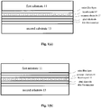
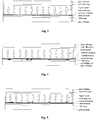
- Fig. 1(b) is a schematic lateral view of another example of the touch display apparatus according to the first embodiment of the present disclosure.
- the touch control display apparatus may have the TN structure.
- Fig. 1(c) illustrates an example of a common electrode layer of the touch display apparatus according to the first embodiment of the present disclosure.
- the shape of the common electrode may be a circle, an ellipse, a triangle, a strip shape, a square or other regular polygon.
- some teeth may be provided at the edges of the common electrode.
- the material of multiple common electrodes is metal oxide such as indium tin oxide (ITO) or graphene.
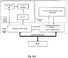
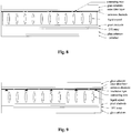
- Fig. 1(d) illustrates an example of a display control circuit and a touch control circuit of the touch display apparatus according to the first embodiment of the present disclosure.
- the touch display apparatus may be connected to a host through a flexible printed circuit.
- the display control circuit and the touch control circuit are provided at two independent chips respectively.
- the display control circuit is connected to data lines and row gate lines of a liquid crystal display section of the touch display apparatus through wires.
- the touch control circuit is connected to touch sensing electrodes (the common electrodes) of a touch sensing section through wires.
- multiple common electrodes are connected to a common level provided to the display control circuit in the case that a display is performed, and each of multiple common electrodes is connected to the touch control circuit as the touch sensing electrode in the case that a touch sensing is performed.
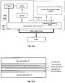
- Fig. 1(e) illustrates another example of the display touch control circuit of the touch display apparatus according to the first embodiment of the present disclosure.
- the touch display apparatus may be connected to a host through a flexible printed circuit.
- the display touch control circuit is a single chip, and the display touch control circuit is connected to data lines and row gate lines of a liquid crystal display section and touch sensing electrodes (the common electrodes) of a touch sensing section.
- multiple common electrodes are connected to a common level provided to the display control circuit in the case that a display is performed, and each of multiple common electrodes is connected to the touch control circuit as the touch sensing electrode in the case that a touch sensing is performed.
- the common electrode is a part of a display module of the display touch screen. Specifically, the common electrode is driven by the common level (Vcom).
- Vcom common level
- the common electrode in combination with different pixel units, creates an electric field across the liquid crystal material at different regions on the screen, so as to control luminous flux of each pixel unit.
- the pixel unit includes pixel transistors and pixel electrodes.
- each pixel unit generally includes three sub pixel units respectively corresponding to red, green and blue, and each of the sub pixel units includes a pixel transistor and a pixel electrode.
- the pixel transistor is a thin film transistor (TFT).
- TFT thin film transistor
- the touch sensing electrodes are separated from a display module, and the display touch screen is formed by superposing a touch screen and a display screen.
- the common electrode is also used as the touch sensing electrode. Therefore, compared with the prior art, a touch sensing electrode layer is removed in the solution of the present disclosure, thus reducing the thickness and the weight of the display touch screen and the optical loss caused by the touch sensing electrode layer, and saving the material and the manufacturing cost.
- the electrical interference between the touch sensing electrode and the display module in the prior art is further reduced.
- the touch sensing electrodes include a row electrode and a column electrode, and noises may be superposed at each row or each column.
- the touch sensing electrode i.e. the common electrodes in the touch sensing process
- the touch sensing electrodes are arranged in a two-dimensional array.
- Each of the touch sensing electrodes is a unit in the array. There is no mutual interference among the units. Matrix units in each row or each column arc different, which will not cause the superposition of noises. Therefore, in the touch display apparatus according to the embodiments of the present disclosure, the amplitude of the greatest noise is greatly reduced and a signal to noise ratio is increased.
- the touch control circuit is configured to detect the self-capacitance of each of the common electrodes.
- the self-capacitance of the common electrode may be the capacitance of the common electrode to the ground.
- the touch control circuit when driving the common electrode, may drive, in response to a signal driving the current common electrode, common electrodes around the current common electrode or the other common electrodes except the current common electrode simultaneously. Moreover, when driving the common electrode, the touch control circuit may also drive the data line simultaneously, in response to a signal driving the current common electrode. In this way, a voltage difference between the detected common electrode and the non-detected common electrode may be reduced, so as to reduce the capacitance of the detected electrode and to prevent a false touch formed by a drip.
- the touch control circuit includes: a signal driving/receiving unit adapted to drive each of the common electrodes and to receive sensed data from each of the common electrodes; and a signal processing unit adapted to determine a touch position according to the sensed data.
- the signal driving/receiving unit may be adapted to drive, in response to a signal driving a current common electrode, common electrodes around the current common electrode or the other common electrodes except the current common electrode simultaneously when the signal driving/receiving unit drives the current common electrode.
- the signal driving/receiving unit may also be configured to drive a data line simultaneously in response to a signal driving a current common electrode, when the signal driving/receiving unit drives the current common electrode.
- the touch control circuit is configured to determine the touch position according to a two-dimensional capacitance variation array.
- the common electrodes may be driven simultaneously or in groups. That is, all of the common electrodes or a part of the common electrodes are detected together.
- the touch sensing electrodes include the row electrodes and the column electrodes
- a progressive scan is adopted and a touch detection time for each frame is long.
- This shortcoming will especially bring negative effects on an In-Cell touch screen.
- the operation of the touch screen is stopped when the display screen is operated, and the operation of the display screen is stopped when the touch screen is operated.
- the In-Cell screen with a working frequency of 60Hz i.e. 16.7ms per frame
- the scanning time for detecting the touch is very short, leading to a lower signal to noise ratio for the existing In-Cell screen.
- each of the electrodes is connected to a touch detection chip.
- the scanning time for detecting the touch may theoretically be equal to the time for detecting one row in the prior art, which may achieve the signal to noise ratio in the prior art.
- T time for detecting one row
- 16Ts 16Ts are spent in scanning the existing structure.
- the shortest time for detecting the touch for each frame is only IT, according to the structure of the embodiments of the present disclosure.
- the display touch control circuit may be configured to execute repeatedly a first step.
- the first step includes: performing a frame scan by the display control circuit and then performing a frame scan by the touch control circuit. That is to say, the display scanning is performed for one frame, and then the touch detection scanning is performed for the frame, and over and over again.
- the display touch control circuit is configured to execute repeatedly a second step.
- the second step includes: performing a frame scan by the touch control circuit and then performing a frame scan by the display control circuit. That is to say, the touch detection scanning is performed for one frame, and then the display scanning is performed for the frame, and over and over again.
- the display scanning may be divided into multiple segments, the touch detection scanning is performed in each of the segments.
- the frequency of the touch detection is multiple times as large as the frequency of the display. Therefore, the frame rate of the touch detection is increased.
- each frame scan performed by the display control circuit is divided into multiple segments, and the touch control circuit performs the scan every time before and after the scan performed by the display control circuit and between the segments.
- the touch display apparatus includes a first substrate 21, a second substrate 23, a liquid crystal layer 25, a common electrode layer 27, a thin film transistor layer and a color filter (CF) layer, in which the liquid crystal layer 25, the common electrode layer 27, the thin film transistor layer and the CF layer are disposed between the first substrate 21 and the second substrate 23.
- the common electrode layer is disposed on the side of the thin film transistor layer facing to the liquid crystal layer.
- the touch display apparatus further includes a second polarizing layer, a first polarizing layer and a cover lens.
- the touch display apparatus has an IPS structure.
- the touch display apparatus may also have an FFS structure in the present embodiment.
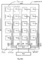
- Fig. 2(b) illustrates a plane view of an example of the common electrode layer according to the second embodiment of the present disclosure.
- the touch display apparatus further includes a display touch control circuit.
- the display touch control circuit includes a display control circuit and a touch control circuit.
- the display touch control circuit is connected to the multiple common electrodes through wires in such a way that the multiple common electrodes are connected to a common level provided to the display control circuit in the case that a display is performed, and each of the multiple common electrodes is connected to the touch control circuit as a touch sensing electrode in the case that a touch sensing is performed.
- the common electrode layer includes the multiple common electrodes (touch sensing electrodes) 1101-1120.
- Fig. 2(b) further illustrates a flexible printed circuit (FPC), a display touch control circuit 29 and a host.
- the touch display apparatus may be connected to the host through the flexible printed circuit.
- the material of the common electrode is metal oxide such as indium tin oxide (ITO) or graphcnc.
- the common electrode may be in the shape of a square, a rectangle, a strip, a diamond or any of other polygons; and may also be in the shape of a triangle, a circle or an ellipse. Furthermore, some teeth may be provided at the edges of the common electrode.
- the patterns of the common electrodes may be consistent or inconsistent. As an example, in Fig. 2(b) , the common electrodes are all in the shape of a square (for example, both the length and the with are equal to 5mm), and the common electrodes are arranged in a rectangular array.
- the chip 29 for the display touch control circuit in Fig. 2(b) is bound onto the substrate in a chip-on-glass (abbreviated as COG) mode.
- COG chip-on-glass
- each of the common electrodes including the corresponding wire
- the screen includes 264 common electrodes.
- the chip 29 for the display touch control circuit packaged in the conventional mode needs at least 264 pins, so that the chip can only be surface-mounted on a printed circuit board. In this case, a very wide flexible printed circuit is necessary. Therefore, the yield is low, and the cost is high.
- the COG mode the chip 29 for the display touch control circuit is directly bound onto the substrate. In such a way, the yield is increased, the package cost is reduced, and the volume of the touch display apparatus is reduced.
- the display touch control circuit 29 is connected to the host through the flexible printed circuit.
- the host communicates with the display touch control circuit 29 through the flexible printed circuit.
- the change in the capacitance of the touch sensing electrode when the touch occurs is proportional to the covered area of the touch sensing electrode. Therefore, the change in the capacitance of each touch sensing electrode indicates the covered area.
- a touch position is determined according to a two-dimensional capacitance variation array.
- the display touch control circuit 29 may be a single chip, in which the display control circuit and the touch control circuit are integrated. Alternatively, the display touch control circuit 29 may include two or more chips, and the display control circuit and the touch control circuit are provided in different chips.
- a driving circuit is provided for the source electrode of each of the thin film transistors, and the driving circuit drives the thin film transistor through a data line.
- the electric field distribution in the liquid crystal layer may be changed by adjusting the voltage of the source electrode of the thin film transistor, so as to reduce the self-capacitance of the common electrode and increase the sensitivity of touch control.
- a touch display apparatus also has an IPS structure or FFS structure.
- the difference between this embodiment and the second embodiment lies in the position of wiring.
- Fig. 4 illustrates an example of wiring according to the third embodiment of the present disclosure, in which wires 501-503 are disposed in a layer different from the layer provided with common electrodes. Specifically, the wires are disposed in a layer provided with pixel electrodes, and the wires may be connected to the respective common electrodes through via holes.
- the material of the wires 501-503 may be metal oxide such as indium tin oxide (ITO) or graphene, or may be a metal.
- the wires 501-503 are disposed right under a black matrix. By disposing the wires under the black matrix, a light reflection probably caused by the metal wires and a trace generated by etching the indium tin oxide may be avoided.
- Fig. 5 illustrates an example of wiring according to the fourth embodiment of the present disclosure, in which wires 501-503 are disposed in a layer different from the layer provided with common electrodes. Specifically, the wires are disposed in an individual layer, which may be connected to the respective common electrodes through via holes.
- Figs. 6(a) and 6(b) illustrate examples of wiring according to the fifth embodiment of the present disclosure, in which wires 501-503 are disposed in a layer different from the layer provided with common electrodes. Specifically, the wires are disposed in a layer provided with data lines. As illustrated in Fig. 6(a) , a data line layer is located under a TFT array. As illustrated in Fig. 6(b) , the data line layer is located on a TFT array. The wires may be connected to the respective common electrodes through via holes.
- Fig. 7 is a schematic lateral view of a touch display apparatus according to the sixth embodiment of the present disclosure.
- the touch display apparatus includes a first substrate 61, a second substrate 63, a liquid crystal layer 65, a common electrode layer 67, a thin film transistor layer and a color filter layer, in which the liquid crystal layer 65, the common electrode layer 67, the thin film transistor layer and the color filter layer arc disposed between the first substrate 61 and the second substrate 63.
- the common electrode layer is disposed on a side of the color filter layer facing to the liquid crystal layer.
- the touch display apparatus further includes a second polarizing layer, a first polarizing layer and a cover lens.
- the touch display apparatus has a TN structure.
- Multiple pixel units are formed in the thin film transistor layer.
- Multiple common electrodes are formed in the common electrode layer, and the multiple common electrodes are arranged in a two-dimensional array.
- a chip for the touch control circuit may be bound onto the substrate in a COG mode.
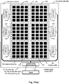
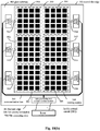
- Fig. 8 illustrates an example of wiring according to the sixth embodiment of the present disclosure.
- the common electrode layer includes multiple sub-regions 301-306, and each of the sub-regions includes multiple common electrodes.
- the shape of the common electrode is a square, a diamond or other polygon, or is a triangle, a circle or an ellipse. Moreover, some leeth may be provided at edges of the common electrode.
- the patterns of the common electrodes may be consistent or inconsistent.
- the material of the common electrode is metal oxide such as indium tin oxide (ITO) or graphene, or is a conductive material such as a metal.
- a common electrode layer is divided into multiple sub-regions.
- Each of the sub-regions includes multiple common electrodes arranged in a two-dimensional array and connected to one driving sensing module.
- the common electrode layer includes multiple sub-regions 301-306, and each of the sub-regions includes multiple common electrodes.
- the shape of the common electrode is a square, a diamond or other polygon, or is a triangle, a circle or an ellipse. Some teeth may be provided at edges of the common electrode.
- the patterns of the respective common electrodes may be consistent or inconsistent.
- the material of the common electrode is metal oxide such as indium tin oxide (ITO) or graphene.
- each of the common electrodes may he respectively connected to one of driving sensing modules 1-6 corresponding to the common electrode through a wire.
- the driving sensing modules 1-6 may be bound onto a substrate in a COG mode.
- the driving sensing modules 1-6 may be connected to a data processing and communication module through a communication bus 700, and the data processing and communication module may be connected to a host through a flexible printed circuit 13.
- the communication bus 700 is disposed in a non-transparent region except a sensing region, and may be a metal oxide line such as indium tin oxide (ITO) line or graphene line, and may also be a metal line.
- ITO indium tin oxide
- the present embodiment is particularly suitable for a large-size screen.
- the two or more display touch control chips may scan a touch panel simultaneously. Therefore, a good image capture rate may be achieved.
Claims (15)
- Appareil d'affichage tactile, caractérisé en ce qu'il comprend :un écran d'affichage tactile comprenant un premier substrat (11, 21), un second substrat (13, 23), une couche de cristaux liquides (15, 25) et une pluralité d'unités de pixels, où chacune des unités de pixel comprend une électrode de pixel et où la couche de cristaux liquides (15, 25) et les unités de pixel sont situées entre le premier substrat et le second substrat, et l'écran d'affichage tactile comprend en outre une pluralité d'électrodes communes (17, 1101-1120) agencées dans une matrice à deux dimensions, où les électrodes communes (17, 1101-1120) sont agencées de manière à créer en combinaison avec les différentes unités de pixel d'un champ électrique à travers le matériau à cristaux liquides, de manière à contrôler le flux lumineux de chaque unité de pixel, etun circuit de commande d'affichage tactile comprenant un circuit de commande d'affichage et un circuit de commande tactile, où le circuit d'affichage de commande tactile est relié à la pluralité d'électrodes communes (17, 1101-1120) par l'intermédiaire de fils, et où la pluralité d'électrodes communes (17, 1101-1120) sont connectées à un niveau commun fourni au circuit de commande d'affichage pendant une phase d'affichage, caractérisé en ce que chacune de la pluralité d'électrodes communes (17, 1101-1120) est reliée au circuit de commande tactile par l'intermédiaire d'un fil indépendant (501-520) comme électrode de détection tactile lors d'une phase de détection tactile.
- Appareil d'affichage tactile selon la revendication 1, où les fils (501-520) sont disposés dans une couche pourvue de la pluralité d'électrodes communes (1101-1120) ou bien les fils (501-503) sont disposés dans une couche différente d'une couche pourvue de la pluralité d'électrodes communes et sont connectées à la pluralité d'électrodes communes par des trous traversants.
- Appareil d'affichage tactile selon la revendication 1, où les fils (501-520) sont disposés dans une couche pourvue de lignes de données, et sont reliés à la pluralité d'électrodes communes (17, 1101-1120) par des trous traversants.
- Appareil d'affichage tactile selon la revendication 1, où les fils (501-520) sont disposés dans une couche munie des électrodes de pixel et sont reliées à la pluralité d'électrodes communes par des trous traversants.
- Appareil d'affichage tactile selon la revendication 1, où les fils (501-520) sont disposés juste sous la matrice noire.
- Appareil d'affichage tactile selon la revendication 1, où le circuit d'affichage de commande tactile (29) est une simple puce, et le circuit de commande d'affichage et le circuit de commande tactile sont intégrés dans la même puce, le circuit d'affichage de commande tactile comprend deux ou plusieurs puces, et le circuit de commande d'affichage et le circuit de commande tactile sont dans différentes puces, ou bien
le circuit écran de contrôle tactile comprend deux ou plusieurs puces, et chacune des puces contrôle une partie de l'écran d'affichage tactile; et éventuellement.
où la puce prévue pour le circuit de commande tactile est collée sur le premier substrat ou le second substrat dans un mode puce sur verre, ou bien la puce prévue pour le circuit de commande d'affichage et la puce prevue pour le circuit de commande tactile sont collées sur le premier substrat ou le second substrat dans un mode puce sur verre. - Appareil d'affichage tactile selon la revendication 1, où le circuit de commande tactile est adapté pour détecter une capacité propre de chacune des électrodes communes (17, 1101-1120) ; et éventuellement
où le circuit de commande tactile est adapté pour détecter la capacité propre d'une électrode commune actuelle par un procédé comprenant :l'entraînement, en réponse à un signal appliqué à l'électrode de courant commune, de l'électrode commune et des électrodes communes de courant autour de l'électrode commune de courant en même temps, oul'entraînement, en réponse à un signal appliqué à l'électrode de courant commune, de l'électrode commune et de toutes les autres électrodes communes de courant en même temps. - Appareil d'affichage tactile selon la revendication 7, où le circuit de commande tactile est adapté pour entraîner simultanément les lignes de données en réponse au signal appliqué à l'électrode commune de courant.
- Appareil d'affichage tactile selon la revendication 7, où le circuit de commande tactile est adapté pour déterminer une position tactile en fonction d'une matrice de détection de capacité en deux dimensions.
- Appareil d'affichage tactile selon la revendication 1, où l'écran d'affichage tactile présente une structure dans le plan de commutation, une structure de commutation de champ de dispersion ou d'une structure nématique en hélice.
- Appareil d'affichage tactile selon la revendication 1, où l'électrode commune (17, 1101-1120) est sous forme de polygone régulier, l'électrode commune (17, 1101-1120) se présente sous la forme d'un rectangle ou l'électrode commune (17, 1101-1120) est sous forme d'un cercle, ou l'électrode commune est sous forme d'ellipse.
- Appareil d'affichage tactile selon la revendication 1, où la structure concave et convexe est prévue au niveau des bords de l'électrode commune (17, 1101-1120).
- Appareil d'affichage tactile selon la revendication 1, où le matériau de la pluralité d'électrodes communes (17, 1101-1120) est de l'oxyde d'étain d'indium ou le graphème ; et éventuellement
où chacune des unités de pixel de l'écran d'affichage tactile comprend un transistor à couche mince, la source du transistor à couche mince est pourvue d'un circuit d'entraînement adapté pour entraîner le transistor à couche mince à travers une ligne de données. - Appareil d'affichage tactile selon la revendication 1, où l'appareil d'affichage tactile comprend une pluralité de circuits de commande tactile, et chacun des circuits de commande tactile est relié à des électrodes communes correspondant à la pluralité d'électrodes communes (17, 1101-1120) ; et éventuellement
où les circuits de commande tactile sont cadencés de façon synchrone, ou bien les circuits de commande tactile fonctionnent en mode de partage du temps. - Appareil d'affichage tactile selon la revendication 1, où le circuit d'affichage de commande tactile est adapté pour exécuter de manière répétée une première étape comprenant : la réalisation d'un balayage par le circuit de commande d'affichage, puis la réalisation d'un balayage par le circuit de commande tactile, ou bien
le circuit de commande écran tactile est adapté pour exécuter de manière répétée une seconde étape comprenant : la réalisation d'un balayage par le circuit de commande tactile, puis la réalisation d'un balayage par le circuit de commande d'affichage ; et éventuellement
où le circuit d'affichage de commande tactile est configuré pour diviser un balayage de trame réalisé par le circuit de commande d'affichage en une pluralité de segments, et réaliser un balayage par le circuit de commande tactile à chaque fois avant le balayage de trame, entre les segments, et après le balayage de trame réalisé par le circuit de commande d'affichage.
Applications Claiming Priority (1)
| Application Number | Priority Date | Filing Date | Title |
|---|---|---|---|
| CN201310223963.3A CN103279245B (zh) | 2013-06-06 | 2013-06-06 | 触控显示装置 |
Publications (2)
| Publication Number | Publication Date |
|---|---|
| EP2811482A1 EP2811482A1 (fr) | 2014-12-10 |
| EP2811482B1 true EP2811482B1 (fr) | 2016-12-07 |
Family
ID=49061798
Family Applications (1)
| Application Number | Title | Priority Date | Filing Date |
|---|---|---|---|
| EP14152427.2A Active EP2811482B1 (fr) | 2013-06-06 | 2014-01-24 | Appareil d'affichage tactile à cristaux liquides |
Country Status (5)
| Country | Link |
|---|---|
| US (1) | US20140362031A1 (fr) |
| EP (1) | EP2811482B1 (fr) |
| JP (1) | JP5989018B2 (fr) |
| KR (1) | KR101608794B1 (fr) |
| CN (1) | CN103279245B (fr) |
Families Citing this family (69)
| Publication number | Priority date | Publication date | Assignee | Title |
|---|---|---|---|---|
| CN103309535A (zh) * | 2013-06-06 | 2013-09-18 | 敦泰科技有限公司 | 电容式触摸屏 |
| CN103455201B (zh) * | 2013-08-27 | 2017-03-29 | 北京京东方光电科技有限公司 | 一种触控显示装置及其驱动方法 |
| CN103472613A (zh) * | 2013-09-13 | 2013-12-25 | 敦泰科技有限公司 | 电容式触摸显示装置 |
| KR101641690B1 (ko) * | 2013-09-25 | 2016-07-21 | 엘지디스플레이 주식회사 | 터치스크린 일체형 표시장치 |
| CN104615291B (zh) * | 2013-11-04 | 2017-12-08 | 凌巨科技股份有限公司 | 显示触控面板的复合驱动电路 |
| CN103713792B (zh) * | 2013-12-23 | 2016-06-01 | 京东方科技集团股份有限公司 | 阵列基板及其制造方法和触摸显示装置 |
| CN103698927B (zh) * | 2013-12-31 | 2017-05-10 | 敦泰电子有限公司 | 触摸显示装置、驱动电路及驱动方法 |
| CN107918235A (zh) * | 2013-12-31 | 2018-04-17 | 上海天马微电子有限公司 | 一种阵列基板及显示装置 |
| CN104808826B (zh) * | 2014-01-28 | 2018-06-15 | 晨星半导体股份有限公司 | 感测电极及感测电极单元 |
| CN103793120A (zh) | 2014-01-28 | 2014-05-14 | 北京京东方光电科技有限公司 | 一种内嵌式触摸屏及显示装置 |
| JP6375223B2 (ja) * | 2014-01-31 | 2018-08-15 | 株式会社ジャパンディスプレイ | センサ付表示装置及びその駆動方法 |
| US9557840B2 (en) * | 2014-02-04 | 2017-01-31 | Apple Inc. | Displays with intra-frame pause |
| CN104598085A (zh) * | 2014-03-13 | 2015-05-06 | 北京智膜科技有限公司 | 一种基于智能膜的触控屏幕控制装置及方法 |
| US10564779B2 (en) * | 2014-04-25 | 2020-02-18 | Boe Technology Group Co., Ltd. | Array substrate and manufacturing method thereof, and touch display device |
| KR101696511B1 (ko) * | 2014-05-19 | 2017-01-16 | 엘지디스플레이 주식회사 | 터치센서 내장형 액정 표시장치 |
| CN104020910B (zh) * | 2014-05-30 | 2017-12-15 | 京东方科技集团股份有限公司 | 一种内嵌式触摸屏及显示装置 |
| CN104020907B (zh) | 2014-05-30 | 2017-02-15 | 京东方科技集团股份有限公司 | 一种内嵌式触摸屏及显示装置 |
| CN104020893B (zh) * | 2014-05-30 | 2017-01-04 | 京东方科技集团股份有限公司 | 一种内嵌式触摸屏及显示装置 |
| CN104020909B (zh) | 2014-05-30 | 2017-06-30 | 京东方科技集团股份有限公司 | 一种内嵌式触摸屏及显示装置 |
| CN104020906B (zh) * | 2014-05-30 | 2016-09-07 | 京东方科技集团股份有限公司 | 一种内嵌式触摸屏以及显示装置 |
| CN104020911A (zh) * | 2014-05-30 | 2014-09-03 | 京东方科技集团股份有限公司 | 一种内嵌式触摸屏及显示装置 |
| CN104020891A (zh) * | 2014-05-30 | 2014-09-03 | 京东方科技集团股份有限公司 | 一种内嵌式触摸屏及显示装置 |
| CN104022128B (zh) * | 2014-05-30 | 2017-02-15 | 京东方科技集团股份有限公司 | 一种阵列基板及其制作方法、以及显示装置 |
| CN104020905B (zh) | 2014-05-30 | 2017-06-16 | 京东方科技集团股份有限公司 | 一种内嵌式触摸屏及显示装置 |
| CN104035640B (zh) | 2014-05-30 | 2017-10-27 | 京东方科技集团股份有限公司 | 一种内嵌式触摸屏及显示装置 |
| CN104123039B (zh) * | 2014-07-10 | 2017-08-01 | 京东方科技集团股份有限公司 | 一种内嵌式触控显示装置及其驱动方法 |
| CN104142772B (zh) | 2014-07-24 | 2017-05-03 | 京东方科技集团股份有限公司 | 一种内嵌式触摸屏及显示装置 |
| KR101597522B1 (ko) * | 2014-08-28 | 2016-02-25 | 주식회사 지2터치 | 신호왜곡 현상을 최소화한 터치패널 및 이를 포함하는 디스플레이장치 |
| US10209834B2 (en) | 2014-10-01 | 2019-02-19 | Microsoft Technology Licensing, Llc | Integrated self-capacitive touch display |
| CN104460080A (zh) * | 2014-12-04 | 2015-03-25 | 深圳市华星光电技术有限公司 | 触控显示装置 |
| CN104484068B (zh) * | 2014-12-09 | 2018-09-18 | 深圳市华星光电技术有限公司 | 一种具有触摸功能的嵌入式显示屏、终端及触摸检测方法 |
| CN104503172A (zh) * | 2014-12-19 | 2015-04-08 | 深圳市华星光电技术有限公司 | 阵列基板及显示装置 |
| US9703439B2 (en) | 2014-12-26 | 2017-07-11 | Lg Display Co., Ltd. | Touch sensor integrated type display device |
| CN104536609B (zh) * | 2014-12-30 | 2018-01-30 | 深圳市华星光电技术有限公司 | 具有触控功能的显示面板以及故障检测方法 |
| JP6765807B2 (ja) * | 2015-01-05 | 2020-10-07 | シナプティクス インコーポレイテッド | 容量性感知を行うための基準電圧の変調 |
| KR102382999B1 (ko) | 2015-01-08 | 2022-04-05 | 삼성디스플레이 주식회사 | 터치 센서를 포함하는 표시 장치 |
| CN104698711B (zh) * | 2015-04-01 | 2018-06-01 | 上海天马微电子有限公司 | 一种阵列基板、显示面板及电子设备 |
| CN104699321B (zh) * | 2015-04-01 | 2018-03-23 | 上海天马微电子有限公司 | 触控显示基板和触控显示装置 |
| CN104699322B (zh) * | 2015-04-01 | 2017-12-29 | 上海天马微电子有限公司 | 阵列基板、触控显示面板、触控显示装置及检测方法 |
| CN107765488B (zh) * | 2015-04-01 | 2019-12-31 | 上海天马微电子有限公司 | 阵列基板、触控显示面板和触控显示装置 |
| CN104699354B (zh) * | 2015-04-01 | 2017-12-22 | 上海天马微电子有限公司 | 触控面板及其驱动方法、触控显示装置 |
| CN104765501B (zh) * | 2015-04-23 | 2018-01-23 | 厦门天马微电子有限公司 | 触控显示面板、装置及其驱动方法 |
| CN104808858B (zh) | 2015-05-08 | 2018-07-10 | 厦门天马微电子有限公司 | 一种触控面板和触控显示装置 |
| CN104793827B (zh) * | 2015-05-08 | 2018-03-27 | 厦门天马微电子有限公司 | 一种阵列基板和自电容式触控显示装置 |
| TWI628566B (zh) * | 2015-05-28 | 2018-07-01 | 鴻海精密工業股份有限公司 | 內嵌式觸控顯示面板 |
| CN106325618A (zh) * | 2015-06-18 | 2017-01-11 | 宸鸿光电科技股份有限公司 | 触控面板 |
| CN104866158B (zh) * | 2015-06-18 | 2017-12-15 | 京东方科技集团股份有限公司 | 一种内嵌式触摸屏及显示装置 |
| CN104866161B (zh) * | 2015-06-23 | 2017-10-27 | 京东方科技集团股份有限公司 | 一种内嵌式触摸屏及显示装置 |
| CN104951162B (zh) * | 2015-07-08 | 2019-01-22 | 京东方科技集团股份有限公司 | 触控显示面板和驱动方法 |
| CN105159486A (zh) * | 2015-07-14 | 2015-12-16 | 京东方科技集团股份有限公司 | Ads阵列基板及其制作方法、显示器件 |
| CN104965628B (zh) * | 2015-07-17 | 2018-03-23 | 合肥京东方光电科技有限公司 | 电容式触控基板和触控显示屏 |
| CN105093721B (zh) * | 2015-08-10 | 2018-03-13 | 上海天马微电子有限公司 | 一种触控显示基板、电子设备及驱动方法 |
| CN105183259B (zh) * | 2015-09-30 | 2018-11-02 | 上海天马微电子有限公司 | 一种触控面板以及触控电子设备 |
| CN105301822B (zh) * | 2015-12-11 | 2018-10-23 | 上海中航光电子有限公司 | 一种阵列基板、显示面板及显示装置 |
| CN105718115B (zh) * | 2016-01-27 | 2019-05-21 | 上海天马微电子有限公司 | 触控显示面板及显示装置 |
| CN105677125B (zh) * | 2016-02-04 | 2018-09-14 | 厦门天马微电子有限公司 | 一种显示面板及其触控信号量的修正方法以及显示面板 |
| JP6588852B2 (ja) | 2016-03-28 | 2019-10-09 | 株式会社ジャパンディスプレイ | センサ及びセンサ付き表示装置 |
| CN105717690A (zh) * | 2016-04-27 | 2016-06-29 | 武汉华星光电技术有限公司 | 内嵌触摸屏及其制备方法、液晶显示器 |
| KR101792524B1 (ko) * | 2016-06-28 | 2017-11-02 | 주식회사 하이딥 | 터치 입력 장치 |
| CN106959556B (zh) * | 2016-09-27 | 2019-09-20 | 关键禾芯科技股份有限公司 | 具有指纹辨识的液晶模块 |
| US20180323239A1 (en) * | 2017-05-03 | 2018-11-08 | Innolux Corporation | Display device |
| CN107132685B (zh) * | 2017-06-23 | 2020-04-17 | 厦门天马微电子有限公司 | 一种显示基板、显示面板和显示装置 |
| US11403983B2 (en) | 2019-09-02 | 2022-08-02 | Samsung Electronics Co., Ltd. | Display controller, display system including the display controller, and method of operating the display controller |
| CN110738973A (zh) * | 2019-09-09 | 2020-01-31 | 福建华佳彩有限公司 | 一种面板驱动方法 |
| CN110570752B (zh) * | 2019-09-11 | 2021-11-02 | Oppo广东移动通信有限公司 | 一种显示屏、电子设备及其控制方法 |
| CN110794988B (zh) * | 2019-10-22 | 2021-12-03 | 维沃移动通信有限公司 | 一种显示模组和电子设备 |
| CN114625329A (zh) | 2020-12-11 | 2022-06-14 | 慧荣科技股份有限公司 | 多屏幕显示控制装置 |
| CN114625330A (zh) | 2020-12-11 | 2022-06-14 | 慧荣科技股份有限公司 | 多屏幕显示控制装置 |
| US11861098B2 (en) * | 2021-06-07 | 2024-01-02 | Wuhan China Star Optoelectronics Semiconductor Display Technology Co., Ltd. | Touch display panel |
Family Cites Families (16)
| Publication number | Priority date | Publication date | Assignee | Title |
|---|---|---|---|---|
| GB0208655D0 (en) * | 2002-04-16 | 2002-05-29 | Koninkl Philips Electronics Nv | Electronic device with display panel and user input function |
| US8040326B2 (en) * | 2007-06-13 | 2011-10-18 | Apple Inc. | Integrated in-plane switching display and touch sensor |
| JP4816668B2 (ja) * | 2008-03-28 | 2011-11-16 | ソニー株式会社 | タッチセンサ付き表示装置 |
| JP4996531B2 (ja) * | 2008-04-23 | 2012-08-08 | 富士通コンポーネント株式会社 | 座標検出装置 |
| US8638314B2 (en) * | 2008-10-17 | 2014-01-28 | Atmel Corporation | Capacitive touch buttons combined with electroluminescent lighting |
| JP5249806B2 (ja) * | 2009-02-16 | 2013-07-31 | グンゼ株式会社 | タッチスイッチ |
| JP2010198615A (ja) * | 2009-02-20 | 2010-09-09 | Acrosense Technology Co Ltd | 静電容量タッチパネル |
| CN101957507B (zh) * | 2009-07-13 | 2012-10-17 | 上海天马微电子有限公司 | 触摸屏液晶显示模组及其触控驱动方法 |
| US8390582B2 (en) * | 2009-08-25 | 2013-03-05 | Apple Inc. | Integrated touch screen |
| CN102109690B (zh) * | 2009-12-25 | 2012-12-19 | 上海天马微电子有限公司 | 内嵌触摸屏液晶显示装置及控制方法 |
| JP2012059073A (ja) * | 2010-09-09 | 2012-03-22 | Bridgestone Corp | 情報表示装置 |
| EP2492784B1 (fr) * | 2011-02-25 | 2021-02-24 | LG Display Co., Ltd. | Dispositif d'affichage intégrant un capteur tactile |
| US9760195B2 (en) * | 2011-09-23 | 2017-09-12 | Apple Inc. | Power management for integrated touch screens |
| JP2013097469A (ja) * | 2011-10-28 | 2013-05-20 | Sharp Corp | タッチパネル駆動装置、表示装置、タッチパネルの駆動方法、プログラムおよび記録媒体 |
| CN103123548B (zh) * | 2011-11-18 | 2016-12-07 | 宸鸿科技(厦门)有限公司 | 触控显示装置 |
| CN203376696U (zh) * | 2013-06-06 | 2014-01-01 | 敦泰科技有限公司 | 触控显示装置 |
-
2013
- 2013-06-06 CN CN201310223963.3A patent/CN103279245B/zh not_active Ceased
- 2013-11-18 US US14/083,223 patent/US20140362031A1/en not_active Abandoned
-
2014
- 2014-01-24 EP EP14152427.2A patent/EP2811482B1/fr active Active
- 2014-02-03 KR KR1020140012304A patent/KR101608794B1/ko active IP Right Grant
- 2014-02-07 JP JP2014022336A patent/JP5989018B2/ja active Active
Non-Patent Citations (1)
| Title |
|---|
| None * |
Also Published As
| Publication number | Publication date |
|---|---|
| EP2811482A1 (fr) | 2014-12-10 |
| CN103279245A (zh) | 2013-09-04 |
| JP5989018B2 (ja) | 2016-09-07 |
| JP2014238816A (ja) | 2014-12-18 |
| CN103279245B (zh) | 2017-03-15 |
| KR101608794B1 (ko) | 2016-04-04 |
| US20140362031A1 (en) | 2014-12-11 |
| KR20140143314A (ko) | 2014-12-16 |
Similar Documents
| Publication | Publication Date | Title |
|---|---|---|
| EP2811482B1 (fr) | Appareil d'affichage tactile à cristaux liquides | |
| US9189117B2 (en) | Touch display device | |
| US10409416B2 (en) | Array substrate, color filter substrate, touch control display device and methods for driving the same | |
| KR102008779B1 (ko) | 터치 스크린 일체형 디스플레이 장치와 이의 구동방법 | |
| US20140362029A1 (en) | Touch display apparatus | |
| US9134560B2 (en) | Integrated touch screen | |
| US7995041B2 (en) | Integrated touch screen | |
| EP2469380B1 (fr) | Écrans tactiles intégrés | |
| CN203376696U (zh) | 触控显示装置 | |
| US20140132534A1 (en) | Display Device Integrated with Touch Screen | |
| CN103488327A (zh) | 触摸传感器集成式显示设备及其制造方法 | |
| KR20110065957A (ko) | 터치 패널 일체형 액정 표시 장치 | |
| WO2015043090A1 (fr) | Panneau d'affichage tactile et dispositif d'affichage tactile | |
| TW201500991A (zh) | 觸控顯示裝置 | |
| KR102230843B1 (ko) | 인셀 터치 액정 표시 장치 | |
| TWI662461B (zh) | 觸控顯示裝置 | |
| TWI502430B (zh) | 觸控顯示裝置 |
Legal Events
| Date | Code | Title | Description |
|---|---|---|---|
| PUAI | Public reference made under article 153(3) epc to a published international application that has entered the european phase |
Free format text: ORIGINAL CODE: 0009012 |
|
| 17P | Request for examination filed |
Effective date: 20140124 |
|
| AK | Designated contracting states |
Kind code of ref document: A1 Designated state(s): AL AT BE BG CH CY CZ DE DK EE ES FI FR GB GR HR HU IE IS IT LI LT LU LV MC MK MT NL NO PL PT RO RS SE SI SK SM TR |
|
| AX | Request for extension of the european patent |
Extension state: BA ME |
|
| RAP1 | Party data changed (applicant data changed or rights of an application transferred) |
Owner name: FOCALTECH ELECTRONICS LTD. |
|
| RIC1 | Information provided on ipc code assigned before grant |
Ipc: G02F 1/1343 20060101ALN20160602BHEP Ipc: G06F 3/041 20060101ALN20160602BHEP Ipc: G09G 3/36 20060101AFI20160602BHEP Ipc: G06F 3/044 20060101ALN20160602BHEP |
|
| GRAP | Despatch of communication of intention to grant a patent |
Free format text: ORIGINAL CODE: EPIDOSNIGR1 |
|
| RIC1 | Information provided on ipc code assigned before grant |
Ipc: G06F 3/044 20060101ALN20160617BHEP Ipc: G06F 3/041 20060101ALN20160617BHEP Ipc: G09G 3/36 20060101AFI20160617BHEP Ipc: G02F 1/1343 20060101ALN20160617BHEP |
|
| RIC1 | Information provided on ipc code assigned before grant |
Ipc: G09G 3/36 20060101AFI20160630BHEP |
|
| RIN1 | Information on inventor provided before grant (corrected) |
Inventor name: MO, LIANGHUA Inventor name: OUYANG, GUANG |
|
| INTG | Intention to grant announced |
Effective date: 20160711 |
|
| GRAS | Grant fee paid |
Free format text: ORIGINAL CODE: EPIDOSNIGR3 |
|
| GRAA | (expected) grant |
Free format text: ORIGINAL CODE: 0009210 |
|
| AK | Designated contracting states |
Kind code of ref document: B1 Designated state(s): AL AT BE BG CH CY CZ DE DK EE ES FI FR GB GR HR HU IE IS IT LI LT LU LV MC MK MT NL NO PL PT RO RS SE SI SK SM TR |
|
| REG | Reference to a national code |
Ref country code: GB Ref legal event code: FG4D |
|
| REG | Reference to a national code |
Ref country code: CH Ref legal event code: EP Ref country code: AT Ref legal event code: REF Ref document number: 852347 Country of ref document: AT Kind code of ref document: T Effective date: 20161215 |
|
| REG | Reference to a national code |
Ref country code: IE Ref legal event code: FG4D |
|
| REG | Reference to a national code |
Ref country code: DE Ref legal event code: R096 Ref document number: 602014005260 Country of ref document: DE |
|
| PG25 | Lapsed in a contracting state [announced via postgrant information from national office to epo] |
Ref country code: LV Free format text: LAPSE BECAUSE OF FAILURE TO SUBMIT A TRANSLATION OF THE DESCRIPTION OR TO PAY THE FEE WITHIN THE PRESCRIBED TIME-LIMIT Effective date: 20161207 |
|
| REG | Reference to a national code |
Ref country code: LT Ref legal event code: MG4D |
|
| REG | Reference to a national code |
Ref country code: NL Ref legal event code: MP Effective date: 20161207 |
|
| PG25 | Lapsed in a contracting state [announced via postgrant information from national office to epo] |
Ref country code: NO Free format text: LAPSE BECAUSE OF FAILURE TO SUBMIT A TRANSLATION OF THE DESCRIPTION OR TO PAY THE FEE WITHIN THE PRESCRIBED TIME-LIMIT Effective date: 20170307 Ref country code: LT Free format text: LAPSE BECAUSE OF FAILURE TO SUBMIT A TRANSLATION OF THE DESCRIPTION OR TO PAY THE FEE WITHIN THE PRESCRIBED TIME-LIMIT Effective date: 20161207 Ref country code: SE Free format text: LAPSE BECAUSE OF FAILURE TO SUBMIT A TRANSLATION OF THE DESCRIPTION OR TO PAY THE FEE WITHIN THE PRESCRIBED TIME-LIMIT Effective date: 20161207 Ref country code: GR Free format text: LAPSE BECAUSE OF FAILURE TO SUBMIT A TRANSLATION OF THE DESCRIPTION OR TO PAY THE FEE WITHIN THE PRESCRIBED TIME-LIMIT Effective date: 20170308 |
|
| REG | Reference to a national code |
Ref country code: AT Ref legal event code: MK05 Ref document number: 852347 Country of ref document: AT Kind code of ref document: T Effective date: 20161207 |
|
| PG25 | Lapsed in a contracting state [announced via postgrant information from national office to epo] |
Ref country code: HR Free format text: LAPSE BECAUSE OF FAILURE TO SUBMIT A TRANSLATION OF THE DESCRIPTION OR TO PAY THE FEE WITHIN THE PRESCRIBED TIME-LIMIT Effective date: 20161207 Ref country code: ES Free format text: LAPSE BECAUSE OF FAILURE TO SUBMIT A TRANSLATION OF THE DESCRIPTION OR TO PAY THE FEE WITHIN THE PRESCRIBED TIME-LIMIT Effective date: 20161207 Ref country code: BE Free format text: LAPSE BECAUSE OF NON-PAYMENT OF DUE FEES Effective date: 20170131 Ref country code: RS Free format text: LAPSE BECAUSE OF FAILURE TO SUBMIT A TRANSLATION OF THE DESCRIPTION OR TO PAY THE FEE WITHIN THE PRESCRIBED TIME-LIMIT Effective date: 20161207 Ref country code: FI Free format text: LAPSE BECAUSE OF FAILURE TO SUBMIT A TRANSLATION OF THE DESCRIPTION OR TO PAY THE FEE WITHIN THE PRESCRIBED TIME-LIMIT Effective date: 20161207 |
|
| PG25 | Lapsed in a contracting state [announced via postgrant information from national office to epo] |
Ref country code: NL Free format text: LAPSE BECAUSE OF FAILURE TO SUBMIT A TRANSLATION OF THE DESCRIPTION OR TO PAY THE FEE WITHIN THE PRESCRIBED TIME-LIMIT Effective date: 20161207 |
|
| PG25 | Lapsed in a contracting state [announced via postgrant information from national office to epo] |
Ref country code: EE Free format text: LAPSE BECAUSE OF FAILURE TO SUBMIT A TRANSLATION OF THE DESCRIPTION OR TO PAY THE FEE WITHIN THE PRESCRIBED TIME-LIMIT Effective date: 20161207 Ref country code: SK Free format text: LAPSE BECAUSE OF FAILURE TO SUBMIT A TRANSLATION OF THE DESCRIPTION OR TO PAY THE FEE WITHIN THE PRESCRIBED TIME-LIMIT Effective date: 20161207 Ref country code: IS Free format text: LAPSE BECAUSE OF FAILURE TO SUBMIT A TRANSLATION OF THE DESCRIPTION OR TO PAY THE FEE WITHIN THE PRESCRIBED TIME-LIMIT Effective date: 20170407 Ref country code: RO Free format text: LAPSE BECAUSE OF FAILURE TO SUBMIT A TRANSLATION OF THE DESCRIPTION OR TO PAY THE FEE WITHIN THE PRESCRIBED TIME-LIMIT Effective date: 20161207 Ref country code: CZ Free format text: LAPSE BECAUSE OF FAILURE TO SUBMIT A TRANSLATION OF THE DESCRIPTION OR TO PAY THE FEE WITHIN THE PRESCRIBED TIME-LIMIT Effective date: 20161207 |
|
| PG25 | Lapsed in a contracting state [announced via postgrant information from national office to epo] |
Ref country code: BE Free format text: LAPSE BECAUSE OF FAILURE TO SUBMIT A TRANSLATION OF THE DESCRIPTION OR TO PAY THE FEE WITHIN THE PRESCRIBED TIME-LIMIT Effective date: 20161207 Ref country code: PT Free format text: LAPSE BECAUSE OF FAILURE TO SUBMIT A TRANSLATION OF THE DESCRIPTION OR TO PAY THE FEE WITHIN THE PRESCRIBED TIME-LIMIT Effective date: 20170407 Ref country code: PL Free format text: LAPSE BECAUSE OF FAILURE TO SUBMIT A TRANSLATION OF THE DESCRIPTION OR TO PAY THE FEE WITHIN THE PRESCRIBED TIME-LIMIT Effective date: 20161207 Ref country code: SM Free format text: LAPSE BECAUSE OF FAILURE TO SUBMIT A TRANSLATION OF THE DESCRIPTION OR TO PAY THE FEE WITHIN THE PRESCRIBED TIME-LIMIT Effective date: 20161207 Ref country code: BG Free format text: LAPSE BECAUSE OF FAILURE TO SUBMIT A TRANSLATION OF THE DESCRIPTION OR TO PAY THE FEE WITHIN THE PRESCRIBED TIME-LIMIT Effective date: 20170307 Ref country code: IT Free format text: LAPSE BECAUSE OF FAILURE TO SUBMIT A TRANSLATION OF THE DESCRIPTION OR TO PAY THE FEE WITHIN THE PRESCRIBED TIME-LIMIT Effective date: 20161207 Ref country code: AT Free format text: LAPSE BECAUSE OF FAILURE TO SUBMIT A TRANSLATION OF THE DESCRIPTION OR TO PAY THE FEE WITHIN THE PRESCRIBED TIME-LIMIT Effective date: 20161207 |
|
| REG | Reference to a national code |
Ref country code: CH Ref legal event code: PL |
|
| REG | Reference to a national code |
Ref country code: DE Ref legal event code: R097 Ref document number: 602014005260 Country of ref document: DE |
|
| PG25 | Lapsed in a contracting state [announced via postgrant information from national office to epo] |
Ref country code: MC Free format text: LAPSE BECAUSE OF FAILURE TO SUBMIT A TRANSLATION OF THE DESCRIPTION OR TO PAY THE FEE WITHIN THE PRESCRIBED TIME-LIMIT Effective date: 20161207 |
|
| PLBE | No opposition filed within time limit |
Free format text: ORIGINAL CODE: 0009261 |
|
| STAA | Information on the status of an ep patent application or granted ep patent |
Free format text: STATUS: NO OPPOSITION FILED WITHIN TIME LIMIT |
|
| REG | Reference to a national code |
Ref country code: FR Ref legal event code: ST Effective date: 20170929 |
|
| PG25 | Lapsed in a contracting state [announced via postgrant information from national office to epo] |
Ref country code: CH Free format text: LAPSE BECAUSE OF NON-PAYMENT OF DUE FEES Effective date: 20170131 Ref country code: FR Free format text: LAPSE BECAUSE OF NON-PAYMENT OF DUE FEES Effective date: 20170207 Ref country code: LI Free format text: LAPSE BECAUSE OF NON-PAYMENT OF DUE FEES Effective date: 20170131 |
|
| REG | Reference to a national code |
Ref country code: IE Ref legal event code: MM4A |
|
| 26N | No opposition filed |
Effective date: 20170908 |
|
| PG25 | Lapsed in a contracting state [announced via postgrant information from national office to epo] |
Ref country code: DK Free format text: LAPSE BECAUSE OF FAILURE TO SUBMIT A TRANSLATION OF THE DESCRIPTION OR TO PAY THE FEE WITHIN THE PRESCRIBED TIME-LIMIT Effective date: 20161207 Ref country code: SI Free format text: LAPSE BECAUSE OF FAILURE TO SUBMIT A TRANSLATION OF THE DESCRIPTION OR TO PAY THE FEE WITHIN THE PRESCRIBED TIME-LIMIT Effective date: 20161207 Ref country code: LU Free format text: LAPSE BECAUSE OF NON-PAYMENT OF DUE FEES Effective date: 20170124 |
|
| PG25 | Lapsed in a contracting state [announced via postgrant information from national office to epo] |
Ref country code: IE Free format text: LAPSE BECAUSE OF NON-PAYMENT OF DUE FEES Effective date: 20170124 |
|
| PG25 | Lapsed in a contracting state [announced via postgrant information from national office to epo] |
Ref country code: MT Free format text: LAPSE BECAUSE OF NON-PAYMENT OF DUE FEES Effective date: 20170124 |
|
| PG25 | Lapsed in a contracting state [announced via postgrant information from national office to epo] |
Ref country code: HU Free format text: LAPSE BECAUSE OF FAILURE TO SUBMIT A TRANSLATION OF THE DESCRIPTION OR TO PAY THE FEE WITHIN THE PRESCRIBED TIME-LIMIT; INVALID AB INITIO Effective date: 20140124 |
|
| PG25 | Lapsed in a contracting state [announced via postgrant information from national office to epo] |
Ref country code: CY Free format text: LAPSE BECAUSE OF FAILURE TO SUBMIT A TRANSLATION OF THE DESCRIPTION OR TO PAY THE FEE WITHIN THE PRESCRIBED TIME-LIMIT Effective date: 20161207 |
|
| PG25 | Lapsed in a contracting state [announced via postgrant information from national office to epo] |
Ref country code: MK Free format text: LAPSE BECAUSE OF FAILURE TO SUBMIT A TRANSLATION OF THE DESCRIPTION OR TO PAY THE FEE WITHIN THE PRESCRIBED TIME-LIMIT Effective date: 20161207 |
|
| PG25 | Lapsed in a contracting state [announced via postgrant information from national office to epo] |
Ref country code: TR Free format text: LAPSE BECAUSE OF FAILURE TO SUBMIT A TRANSLATION OF THE DESCRIPTION OR TO PAY THE FEE WITHIN THE PRESCRIBED TIME-LIMIT Effective date: 20161207 |
|
| PG25 | Lapsed in a contracting state [announced via postgrant information from national office to epo] |
Ref country code: AL Free format text: LAPSE BECAUSE OF FAILURE TO SUBMIT A TRANSLATION OF THE DESCRIPTION OR TO PAY THE FEE WITHIN THE PRESCRIBED TIME-LIMIT Effective date: 20161207 |
|
| PGFP | Annual fee paid to national office [announced via postgrant information from national office to epo] |
Ref country code: GB Payment date: 20230127 Year of fee payment: 10 Ref country code: DE Payment date: 20230127 Year of fee payment: 10 |
|
| P01 | Opt-out of the competence of the unified patent court (upc) registered |
Effective date: 20230526 |
|
| PGFP | Annual fee paid to national office [announced via postgrant information from national office to epo] |
Ref country code: DE Payment date: 20240129 Year of fee payment: 11 Ref country code: GB Payment date: 20240129 Year of fee payment: 11 |