EP2811482B1 - Touch liquid crystal display device - Google Patents
Touch liquid crystal display device Download PDFInfo
- Publication number
- EP2811482B1 EP2811482B1 EP14152427.2A EP14152427A EP2811482B1 EP 2811482 B1 EP2811482 B1 EP 2811482B1 EP 14152427 A EP14152427 A EP 14152427A EP 2811482 B1 EP2811482 B1 EP 2811482B1
- Authority
- EP
- European Patent Office
- Prior art keywords
- touch
- control circuit
- display
- touch control
- common electrodes
- Prior art date
- Legal status (The legal status is an assumption and is not a legal conclusion. Google has not performed a legal analysis and makes no representation as to the accuracy of the status listed.)
- Active
Links
Images


Classifications
-
- G—PHYSICS
- G06—COMPUTING OR CALCULATING; COUNTING
- G06F—ELECTRIC DIGITAL DATA PROCESSING
- G06F3/00—Input arrangements for transferring data to be processed into a form capable of being handled by the computer; Output arrangements for transferring data from processing unit to output unit, e.g. interface arrangements
- G06F3/01—Input arrangements or combined input and output arrangements for interaction between user and computer
- G06F3/03—Arrangements for converting the position or the displacement of a member into a coded form
- G06F3/041—Digitisers, e.g. for touch screens or touch pads, characterised by the transducing means
- G06F3/044—Digitisers, e.g. for touch screens or touch pads, characterised by the transducing means by capacitive means
- G06F3/0443—Digitisers, e.g. for touch screens or touch pads, characterised by the transducing means by capacitive means using a single layer of sensing electrodes
-
- G—PHYSICS
- G06—COMPUTING OR CALCULATING; COUNTING
- G06F—ELECTRIC DIGITAL DATA PROCESSING
- G06F3/00—Input arrangements for transferring data to be processed into a form capable of being handled by the computer; Output arrangements for transferring data from processing unit to output unit, e.g. interface arrangements
- G06F3/01—Input arrangements or combined input and output arrangements for interaction between user and computer
- G06F3/03—Arrangements for converting the position or the displacement of a member into a coded form
- G06F3/041—Digitisers, e.g. for touch screens or touch pads, characterised by the transducing means
- G06F3/0412—Digitisers structurally integrated in a display
-
- G—PHYSICS
- G02—OPTICS
- G02F—OPTICAL DEVICES OR ARRANGEMENTS FOR THE CONTROL OF LIGHT BY MODIFICATION OF THE OPTICAL PROPERTIES OF THE MEDIA OF THE ELEMENTS INVOLVED THEREIN; NON-LINEAR OPTICS; FREQUENCY-CHANGING OF LIGHT; OPTICAL LOGIC ELEMENTS; OPTICAL ANALOGUE/DIGITAL CONVERTERS
- G02F1/00—Devices or arrangements for the control of the intensity, colour, phase, polarisation or direction of light arriving from an independent light source, e.g. switching, gating or modulating; Non-linear optics
- G02F1/01—Devices or arrangements for the control of the intensity, colour, phase, polarisation or direction of light arriving from an independent light source, e.g. switching, gating or modulating; Non-linear optics for the control of the intensity, phase, polarisation or colour
- G02F1/13—Devices or arrangements for the control of the intensity, colour, phase, polarisation or direction of light arriving from an independent light source, e.g. switching, gating or modulating; Non-linear optics for the control of the intensity, phase, polarisation or colour based on liquid crystals, e.g. single liquid crystal display cells
- G02F1/133—Constructional arrangements; Operation of liquid crystal cells; Circuit arrangements
- G02F1/1333—Constructional arrangements; Manufacturing methods
- G02F1/13338—Input devices, e.g. touch panels
-
- G—PHYSICS
- G02—OPTICS
- G02F—OPTICAL DEVICES OR ARRANGEMENTS FOR THE CONTROL OF LIGHT BY MODIFICATION OF THE OPTICAL PROPERTIES OF THE MEDIA OF THE ELEMENTS INVOLVED THEREIN; NON-LINEAR OPTICS; FREQUENCY-CHANGING OF LIGHT; OPTICAL LOGIC ELEMENTS; OPTICAL ANALOGUE/DIGITAL CONVERTERS
- G02F1/00—Devices or arrangements for the control of the intensity, colour, phase, polarisation or direction of light arriving from an independent light source, e.g. switching, gating or modulating; Non-linear optics
- G02F1/01—Devices or arrangements for the control of the intensity, colour, phase, polarisation or direction of light arriving from an independent light source, e.g. switching, gating or modulating; Non-linear optics for the control of the intensity, phase, polarisation or colour
- G02F1/13—Devices or arrangements for the control of the intensity, colour, phase, polarisation or direction of light arriving from an independent light source, e.g. switching, gating or modulating; Non-linear optics for the control of the intensity, phase, polarisation or colour based on liquid crystals, e.g. single liquid crystal display cells
- G02F1/133—Constructional arrangements; Operation of liquid crystal cells; Circuit arrangements
- G02F1/1333—Constructional arrangements; Manufacturing methods
- G02F1/1343—Electrodes
- G02F1/134309—Electrodes characterised by their geometrical arrangement
-
- G—PHYSICS
- G06—COMPUTING OR CALCULATING; COUNTING
- G06F—ELECTRIC DIGITAL DATA PROCESSING
- G06F3/00—Input arrangements for transferring data to be processed into a form capable of being handled by the computer; Output arrangements for transferring data from processing unit to output unit, e.g. interface arrangements
- G06F3/01—Input arrangements or combined input and output arrangements for interaction between user and computer
- G06F3/03—Arrangements for converting the position or the displacement of a member into a coded form
- G06F3/041—Digitisers, e.g. for touch screens or touch pads, characterised by the transducing means
- G06F3/0416—Control or interface arrangements specially adapted for digitisers
- G06F3/04166—Details of scanning methods, e.g. sampling time, grouping of sub areas or time sharing with display driving
-
- G—PHYSICS
- G06—COMPUTING OR CALCULATING; COUNTING
- G06F—ELECTRIC DIGITAL DATA PROCESSING
- G06F3/00—Input arrangements for transferring data to be processed into a form capable of being handled by the computer; Output arrangements for transferring data from processing unit to output unit, e.g. interface arrangements
- G06F3/01—Input arrangements or combined input and output arrangements for interaction between user and computer
- G06F3/03—Arrangements for converting the position or the displacement of a member into a coded form
- G06F3/041—Digitisers, e.g. for touch screens or touch pads, characterised by the transducing means
- G06F3/0416—Control or interface arrangements specially adapted for digitisers
- G06F3/0418—Control or interface arrangements specially adapted for digitisers for error correction or compensation, e.g. based on parallax, calibration or alignment
- G06F3/04184—Synchronisation with the driving of the display or the backlighting unit to avoid interferences generated internally
-
- G—PHYSICS
- G06—COMPUTING OR CALCULATING; COUNTING
- G06F—ELECTRIC DIGITAL DATA PROCESSING
- G06F3/00—Input arrangements for transferring data to be processed into a form capable of being handled by the computer; Output arrangements for transferring data from processing unit to output unit, e.g. interface arrangements
- G06F3/01—Input arrangements or combined input and output arrangements for interaction between user and computer
- G06F3/03—Arrangements for converting the position or the displacement of a member into a coded form
- G06F3/041—Digitisers, e.g. for touch screens or touch pads, characterised by the transducing means
- G06F3/044—Digitisers, e.g. for touch screens or touch pads, characterised by the transducing means by capacitive means
- G06F3/0445—Digitisers, e.g. for touch screens or touch pads, characterised by the transducing means by capacitive means using two or more layers of sensing electrodes, e.g. using two layers of electrodes separated by a dielectric layer
-
- G—PHYSICS
- G06—COMPUTING OR CALCULATING; COUNTING
- G06F—ELECTRIC DIGITAL DATA PROCESSING
- G06F3/00—Input arrangements for transferring data to be processed into a form capable of being handled by the computer; Output arrangements for transferring data from processing unit to output unit, e.g. interface arrangements
- G06F3/01—Input arrangements or combined input and output arrangements for interaction between user and computer
- G06F3/03—Arrangements for converting the position or the displacement of a member into a coded form
- G06F3/041—Digitisers, e.g. for touch screens or touch pads, characterised by the transducing means
- G06F3/044—Digitisers, e.g. for touch screens or touch pads, characterised by the transducing means by capacitive means
- G06F3/0446—Digitisers, e.g. for touch screens or touch pads, characterised by the transducing means by capacitive means using a grid-like structure of electrodes in at least two directions, e.g. using row and column electrodes
-
- G—PHYSICS
- G09—EDUCATION; CRYPTOGRAPHY; DISPLAY; ADVERTISING; SEALS
- G09G—ARRANGEMENTS OR CIRCUITS FOR CONTROL OF INDICATING DEVICES USING STATIC MEANS TO PRESENT VARIABLE INFORMATION
- G09G3/00—Control arrangements or circuits, of interest only in connection with visual indicators other than cathode-ray tubes
- G09G3/20—Control arrangements or circuits, of interest only in connection with visual indicators other than cathode-ray tubes for presentation of an assembly of a number of characters, e.g. a page, by composing the assembly by combination of individual elements arranged in a matrix no fixed position being assigned to or needed to be assigned to the individual characters or partial characters
- G09G3/34—Control arrangements or circuits, of interest only in connection with visual indicators other than cathode-ray tubes for presentation of an assembly of a number of characters, e.g. a page, by composing the assembly by combination of individual elements arranged in a matrix no fixed position being assigned to or needed to be assigned to the individual characters or partial characters by control of light from an independent source
- G09G3/36—Control arrangements or circuits, of interest only in connection with visual indicators other than cathode-ray tubes for presentation of an assembly of a number of characters, e.g. a page, by composing the assembly by combination of individual elements arranged in a matrix no fixed position being assigned to or needed to be assigned to the individual characters or partial characters by control of light from an independent source using liquid crystals
-
- G—PHYSICS
- G02—OPTICS
- G02F—OPTICAL DEVICES OR ARRANGEMENTS FOR THE CONTROL OF LIGHT BY MODIFICATION OF THE OPTICAL PROPERTIES OF THE MEDIA OF THE ELEMENTS INVOLVED THEREIN; NON-LINEAR OPTICS; FREQUENCY-CHANGING OF LIGHT; OPTICAL LOGIC ELEMENTS; OPTICAL ANALOGUE/DIGITAL CONVERTERS
- G02F1/00—Devices or arrangements for the control of the intensity, colour, phase, polarisation or direction of light arriving from an independent light source, e.g. switching, gating or modulating; Non-linear optics
- G02F1/01—Devices or arrangements for the control of the intensity, colour, phase, polarisation or direction of light arriving from an independent light source, e.g. switching, gating or modulating; Non-linear optics for the control of the intensity, phase, polarisation or colour
- G02F1/13—Devices or arrangements for the control of the intensity, colour, phase, polarisation or direction of light arriving from an independent light source, e.g. switching, gating or modulating; Non-linear optics for the control of the intensity, phase, polarisation or colour based on liquid crystals, e.g. single liquid crystal display cells
- G02F1/133—Constructional arrangements; Operation of liquid crystal cells; Circuit arrangements
- G02F1/1333—Constructional arrangements; Manufacturing methods
- G02F1/1343—Electrodes
- G02F1/134309—Electrodes characterised by their geometrical arrangement
- G02F1/134363—Electrodes characterised by their geometrical arrangement for applying an electric field parallel to the substrate, i.e. in-plane switching [IPS]
-
- G—PHYSICS
- G02—OPTICS
- G02F—OPTICAL DEVICES OR ARRANGEMENTS FOR THE CONTROL OF LIGHT BY MODIFICATION OF THE OPTICAL PROPERTIES OF THE MEDIA OF THE ELEMENTS INVOLVED THEREIN; NON-LINEAR OPTICS; FREQUENCY-CHANGING OF LIGHT; OPTICAL LOGIC ELEMENTS; OPTICAL ANALOGUE/DIGITAL CONVERTERS
- G02F2201/00—Constructional arrangements not provided for in groups G02F1/00 - G02F7/00
- G02F2201/12—Constructional arrangements not provided for in groups G02F1/00 - G02F7/00 electrode
- G02F2201/121—Constructional arrangements not provided for in groups G02F1/00 - G02F7/00 electrode common or background
-
- G—PHYSICS
- G06—COMPUTING OR CALCULATING; COUNTING
- G06F—ELECTRIC DIGITAL DATA PROCESSING
- G06F3/00—Input arrangements for transferring data to be processed into a form capable of being handled by the computer; Output arrangements for transferring data from processing unit to output unit, e.g. interface arrangements
- G06F3/01—Input arrangements or combined input and output arrangements for interaction between user and computer
- G06F3/03—Arrangements for converting the position or the displacement of a member into a coded form
- G06F3/041—Digitisers, e.g. for touch screens or touch pads, characterised by the transducing means
- G06F3/0416—Control or interface arrangements specially adapted for digitisers
- G06F3/04164—Connections between sensors and controllers, e.g. routing lines between electrodes and connection pads
Definitions
- An integrated touch screen can include multi-function circuit elements that form part of the display circuitry of the display system that generates an image on the display, and also form part of the touch sensing circuitry of a touch sensing system that senses one or more touches on or near the display.
- the multi-function circuit elements can be, for example, capacitors in display pixels of an LCD that are configured to operate as display circuitry in the display system, and that may also be configured to operate as touch circuitry of the touch sensing system.
- one or more circuit elements of the display pixel stackup can form a conductive portion of the touch sensing system, such as a charge collector, which can be operated with switches and conductive lines to sense touch.
- a touch display apparatus is provided according to the embodiments of the present disclosure to solve at least one of the above-mentioned problems.
- the wires are disposed in a layer provided with the pixel electrodes, and are connected to the multiple common electrodes through via holes.
- the chip of the display control circuit and the chip of the touch control circuit are bound onto the first substrate or the second substrate in chip-on-glass mode.
- the touch control circuit is adapted to determine a touch position according to a two-dimensional capacitance sensing array.
- the display touch screen has an in-plane switching structure, a fringe field switching structure, or a twisted nematic structure.
- Concave and convex structure is provided at edges of the common electrode.
- the material of multiple common electrodes is metal oxide such as indium tin oxide or graphene.
- the touch control display apparatus includes multiple touch control circuits, and each of the touch control circuits is connected to the corresponding common electrodes in multiple common electrodes.
- the display touch screen may have an in-plane switching (abbreviated as IPS) structure, a fringe field switching (abbreviated as FFS) structure, or a twisted nematic (abbreviated as TN) structure.
- IPS in-plane switching
- FFS fringe field switching
- TN twisted nematic
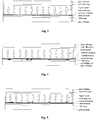
- Fig. 1(b) is a schematic lateral view of another example of the touch display apparatus according to the first embodiment of the present disclosure.
- the touch control display apparatus may have the TN structure.
- Fig. 1(c) illustrates an example of a common electrode layer of the touch display apparatus according to the first embodiment of the present disclosure.
- the shape of the common electrode may be a circle, an ellipse, a triangle, a strip shape, a square or other regular polygon.
- some teeth may be provided at the edges of the common electrode.
- the material of multiple common electrodes is metal oxide such as indium tin oxide (ITO) or graphene.
- Fig. 1(d) illustrates an example of a display control circuit and a touch control circuit of the touch display apparatus according to the first embodiment of the present disclosure.
- the touch display apparatus may be connected to a host through a flexible printed circuit.
- the display control circuit and the touch control circuit are provided at two independent chips respectively.
- the display control circuit is connected to data lines and row gate lines of a liquid crystal display section of the touch display apparatus through wires.
- the touch control circuit is connected to touch sensing electrodes (the common electrodes) of a touch sensing section through wires.
- multiple common electrodes are connected to a common level provided to the display control circuit in the case that a display is performed, and each of multiple common electrodes is connected to the touch control circuit as the touch sensing electrode in the case that a touch sensing is performed.
- Fig. 1(e) illustrates another example of the display touch control circuit of the touch display apparatus according to the first embodiment of the present disclosure.
- the touch display apparatus may be connected to a host through a flexible printed circuit.
- the display touch control circuit is a single chip, and the display touch control circuit is connected to data lines and row gate lines of a liquid crystal display section and touch sensing electrodes (the common electrodes) of a touch sensing section.
- multiple common electrodes are connected to a common level provided to the display control circuit in the case that a display is performed, and each of multiple common electrodes is connected to the touch control circuit as the touch sensing electrode in the case that a touch sensing is performed.
- the common electrode is a part of a display module of the display touch screen. Specifically, the common electrode is driven by the common level (Vcom).
- Vcom common level
- the common electrode in combination with different pixel units, creates an electric field across the liquid crystal material at different regions on the screen, so as to control luminous flux of each pixel unit.
- the pixel unit includes pixel transistors and pixel electrodes.
- each pixel unit generally includes three sub pixel units respectively corresponding to red, green and blue, and each of the sub pixel units includes a pixel transistor and a pixel electrode.
- the pixel transistor is a thin film transistor (TFT).
- TFT thin film transistor
- the touch sensing electrodes are separated from a display module, and the display touch screen is formed by superposing a touch screen and a display screen.
- the common electrode is also used as the touch sensing electrode. Therefore, compared with the prior art, a touch sensing electrode layer is removed in the solution of the present disclosure, thus reducing the thickness and the weight of the display touch screen and the optical loss caused by the touch sensing electrode layer, and saving the material and the manufacturing cost.
- the electrical interference between the touch sensing electrode and the display module in the prior art is further reduced.
- the touch sensing electrodes include a row electrode and a column electrode, and noises may be superposed at each row or each column.
- the touch sensing electrode i.e. the common electrodes in the touch sensing process
- the touch sensing electrodes are arranged in a two-dimensional array.
- Each of the touch sensing electrodes is a unit in the array. There is no mutual interference among the units. Matrix units in each row or each column arc different, which will not cause the superposition of noises. Therefore, in the touch display apparatus according to the embodiments of the present disclosure, the amplitude of the greatest noise is greatly reduced and a signal to noise ratio is increased.
- the touch control circuit is configured to detect the self-capacitance of each of the common electrodes.
- the self-capacitance of the common electrode may be the capacitance of the common electrode to the ground.
- the touch control circuit when driving the common electrode, may drive, in response to a signal driving the current common electrode, common electrodes around the current common electrode or the other common electrodes except the current common electrode simultaneously. Moreover, when driving the common electrode, the touch control circuit may also drive the data line simultaneously, in response to a signal driving the current common electrode. In this way, a voltage difference between the detected common electrode and the non-detected common electrode may be reduced, so as to reduce the capacitance of the detected electrode and to prevent a false touch formed by a drip.
- the touch control circuit includes: a signal driving/receiving unit adapted to drive each of the common electrodes and to receive sensed data from each of the common electrodes; and a signal processing unit adapted to determine a touch position according to the sensed data.
- the signal driving/receiving unit may be adapted to drive, in response to a signal driving a current common electrode, common electrodes around the current common electrode or the other common electrodes except the current common electrode simultaneously when the signal driving/receiving unit drives the current common electrode.
- the signal driving/receiving unit may also be configured to drive a data line simultaneously in response to a signal driving a current common electrode, when the signal driving/receiving unit drives the current common electrode.
- the touch control circuit is configured to determine the touch position according to a two-dimensional capacitance variation array.
- the common electrodes may be driven simultaneously or in groups. That is, all of the common electrodes or a part of the common electrodes are detected together.
- the touch sensing electrodes include the row electrodes and the column electrodes
- a progressive scan is adopted and a touch detection time for each frame is long.
- This shortcoming will especially bring negative effects on an In-Cell touch screen.
- the operation of the touch screen is stopped when the display screen is operated, and the operation of the display screen is stopped when the touch screen is operated.
- the In-Cell screen with a working frequency of 60Hz i.e. 16.7ms per frame
- the scanning time for detecting the touch is very short, leading to a lower signal to noise ratio for the existing In-Cell screen.
- each of the electrodes is connected to a touch detection chip.
- the scanning time for detecting the touch may theoretically be equal to the time for detecting one row in the prior art, which may achieve the signal to noise ratio in the prior art.
- T time for detecting one row
- 16Ts 16Ts are spent in scanning the existing structure.
- the shortest time for detecting the touch for each frame is only IT, according to the structure of the embodiments of the present disclosure.
- the display touch control circuit may be configured to execute repeatedly a first step.
- the first step includes: performing a frame scan by the display control circuit and then performing a frame scan by the touch control circuit. That is to say, the display scanning is performed for one frame, and then the touch detection scanning is performed for the frame, and over and over again.
- the display touch control circuit is configured to execute repeatedly a second step.
- the second step includes: performing a frame scan by the touch control circuit and then performing a frame scan by the display control circuit. That is to say, the touch detection scanning is performed for one frame, and then the display scanning is performed for the frame, and over and over again.
- the display scanning may be divided into multiple segments, the touch detection scanning is performed in each of the segments.
- the frequency of the touch detection is multiple times as large as the frequency of the display. Therefore, the frame rate of the touch detection is increased.
- each frame scan performed by the display control circuit is divided into multiple segments, and the touch control circuit performs the scan every time before and after the scan performed by the display control circuit and between the segments.
- the touch display apparatus includes a first substrate 21, a second substrate 23, a liquid crystal layer 25, a common electrode layer 27, a thin film transistor layer and a color filter (CF) layer, in which the liquid crystal layer 25, the common electrode layer 27, the thin film transistor layer and the CF layer are disposed between the first substrate 21 and the second substrate 23.
- the common electrode layer is disposed on the side of the thin film transistor layer facing to the liquid crystal layer.
- the touch display apparatus further includes a second polarizing layer, a first polarizing layer and a cover lens.
- the touch display apparatus has an IPS structure.
- the touch display apparatus may also have an FFS structure in the present embodiment.
- Fig. 2(b) illustrates a plane view of an example of the common electrode layer according to the second embodiment of the present disclosure.
- the touch display apparatus further includes a display touch control circuit.
- the display touch control circuit includes a display control circuit and a touch control circuit.
- the display touch control circuit is connected to the multiple common electrodes through wires in such a way that the multiple common electrodes are connected to a common level provided to the display control circuit in the case that a display is performed, and each of the multiple common electrodes is connected to the touch control circuit as a touch sensing electrode in the case that a touch sensing is performed.
- the common electrode layer includes the multiple common electrodes (touch sensing electrodes) 1101-1120.
- Fig. 2(b) further illustrates a flexible printed circuit (FPC), a display touch control circuit 29 and a host.
- the touch display apparatus may be connected to the host through the flexible printed circuit.
- the material of the common electrode is metal oxide such as indium tin oxide (ITO) or graphcnc.
- the common electrode may be in the shape of a square, a rectangle, a strip, a diamond or any of other polygons; and may also be in the shape of a triangle, a circle or an ellipse. Furthermore, some teeth may be provided at the edges of the common electrode.
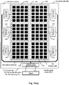
- the patterns of the common electrodes may be consistent or inconsistent. As an example, in Fig. 2(b) , the common electrodes are all in the shape of a square (for example, both the length and the with are equal to 5mm), and the common electrodes are arranged in a rectangular array.
- the chip 29 for the display touch control circuit in Fig. 2(b) is bound onto the substrate in a chip-on-glass (abbreviated as COG) mode.
- COG chip-on-glass
- each of the common electrodes including the corresponding wire
- the screen includes 264 common electrodes.
- the chip 29 for the display touch control circuit packaged in the conventional mode needs at least 264 pins, so that the chip can only be surface-mounted on a printed circuit board. In this case, a very wide flexible printed circuit is necessary. Therefore, the yield is low, and the cost is high.
- the COG mode the chip 29 for the display touch control circuit is directly bound onto the substrate. In such a way, the yield is increased, the package cost is reduced, and the volume of the touch display apparatus is reduced.
- the display touch control circuit 29 is connected to the host through the flexible printed circuit.
- the host communicates with the display touch control circuit 29 through the flexible printed circuit.
- the change in the capacitance of the touch sensing electrode when the touch occurs is proportional to the covered area of the touch sensing electrode. Therefore, the change in the capacitance of each touch sensing electrode indicates the covered area.
- a touch position is determined according to a two-dimensional capacitance variation array.
- the display touch control circuit 29 may be a single chip, in which the display control circuit and the touch control circuit are integrated. Alternatively, the display touch control circuit 29 may include two or more chips, and the display control circuit and the touch control circuit are provided in different chips.
- a driving circuit is provided for the source electrode of each of the thin film transistors, and the driving circuit drives the thin film transistor through a data line.
- the electric field distribution in the liquid crystal layer may be changed by adjusting the voltage of the source electrode of the thin film transistor, so as to reduce the self-capacitance of the common electrode and increase the sensitivity of touch control.
- a touch display apparatus also has an IPS structure or FFS structure.
- the difference between this embodiment and the second embodiment lies in the position of wiring.
- Fig. 4 illustrates an example of wiring according to the third embodiment of the present disclosure, in which wires 501-503 are disposed in a layer different from the layer provided with common electrodes. Specifically, the wires are disposed in a layer provided with pixel electrodes, and the wires may be connected to the respective common electrodes through via holes.
- the material of the wires 501-503 may be metal oxide such as indium tin oxide (ITO) or graphene, or may be a metal.
- the wires 501-503 are disposed right under a black matrix. By disposing the wires under the black matrix, a light reflection probably caused by the metal wires and a trace generated by etching the indium tin oxide may be avoided.
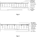
- Fig. 5 illustrates an example of wiring according to the fourth embodiment of the present disclosure, in which wires 501-503 are disposed in a layer different from the layer provided with common electrodes. Specifically, the wires are disposed in an individual layer, which may be connected to the respective common electrodes through via holes.
- Figs. 6(a) and 6(b) illustrate examples of wiring according to the fifth embodiment of the present disclosure, in which wires 501-503 are disposed in a layer different from the layer provided with common electrodes. Specifically, the wires are disposed in a layer provided with data lines. As illustrated in Fig. 6(a) , a data line layer is located under a TFT array. As illustrated in Fig. 6(b) , the data line layer is located on a TFT array. The wires may be connected to the respective common electrodes through via holes.
- Fig. 7 is a schematic lateral view of a touch display apparatus according to the sixth embodiment of the present disclosure.
- the touch display apparatus includes a first substrate 61, a second substrate 63, a liquid crystal layer 65, a common electrode layer 67, a thin film transistor layer and a color filter layer, in which the liquid crystal layer 65, the common electrode layer 67, the thin film transistor layer and the color filter layer arc disposed between the first substrate 61 and the second substrate 63.
- the common electrode layer is disposed on a side of the color filter layer facing to the liquid crystal layer.
- the touch display apparatus further includes a second polarizing layer, a first polarizing layer and a cover lens.
- the touch display apparatus has a TN structure.
- Multiple pixel units are formed in the thin film transistor layer.
- Multiple common electrodes are formed in the common electrode layer, and the multiple common electrodes are arranged in a two-dimensional array.
- a chip for the touch control circuit may be bound onto the substrate in a COG mode.
- Fig. 8 illustrates an example of wiring according to the sixth embodiment of the present disclosure.
- the common electrode layer includes multiple sub-regions 301-306, and each of the sub-regions includes multiple common electrodes.
- the shape of the common electrode is a square, a diamond or other polygon, or is a triangle, a circle or an ellipse. Moreover, some leeth may be provided at edges of the common electrode.
- the patterns of the common electrodes may be consistent or inconsistent.
- the material of the common electrode is metal oxide such as indium tin oxide (ITO) or graphene, or is a conductive material such as a metal.
- a common electrode layer is divided into multiple sub-regions.
- Each of the sub-regions includes multiple common electrodes arranged in a two-dimensional array and connected to one driving sensing module.
- the common electrode layer includes multiple sub-regions 301-306, and each of the sub-regions includes multiple common electrodes.
- the shape of the common electrode is a square, a diamond or other polygon, or is a triangle, a circle or an ellipse. Some teeth may be provided at edges of the common electrode.
- the patterns of the respective common electrodes may be consistent or inconsistent.
- the material of the common electrode is metal oxide such as indium tin oxide (ITO) or graphene.
- each of the common electrodes may he respectively connected to one of driving sensing modules 1-6 corresponding to the common electrode through a wire.
- the driving sensing modules 1-6 may be bound onto a substrate in a COG mode.
- the driving sensing modules 1-6 may be connected to a data processing and communication module through a communication bus 700, and the data processing and communication module may be connected to a host through a flexible printed circuit 13.
- the communication bus 700 is disposed in a non-transparent region except a sensing region, and may be a metal oxide line such as indium tin oxide (ITO) line or graphene line, and may also be a metal line.
- ITO indium tin oxide
- the present embodiment is particularly suitable for a large-size screen.
- the two or more display touch control chips may scan a touch panel simultaneously. Therefore, a good image capture rate may be achieved.
Landscapes
- Engineering & Computer Science (AREA)
- Physics & Mathematics (AREA)
- Theoretical Computer Science (AREA)
- General Engineering & Computer Science (AREA)
- General Physics & Mathematics (AREA)
- Nonlinear Science (AREA)
- Human Computer Interaction (AREA)
- Crystallography & Structural Chemistry (AREA)
- Chemical & Material Sciences (AREA)
- Mathematical Physics (AREA)
- Optics & Photonics (AREA)
- Computer Hardware Design (AREA)
- Geometry (AREA)
- Liquid Crystal (AREA)
- Position Input By Displaying (AREA)
- Devices For Indicating Variable Information By Combining Individual Elements (AREA)
Description
- This application claims the priority to Chinese Patent Application No.
201310223963.3 - The present invention relates to the field of touch technology, and in particular to a touch display apparatus.
- Currently, a capacitive touch screen is widely applied in various electronic products, and gradually becomes popular in the people's work and life. The size of the capacitive touch screen is continuously increased, for example, a smart mobile phone of 3-6.1 inches and a tablet of larger than 10 inches. Moreover, the application filed of the capacitive touch screen may be further extended to a smart television and the like. However, the existing capacitive touch screen generally has some problems such as poor anti-interference performance, low frame rate, larger thickness and high complexity in manufacturing process.
US2011050585 provides displays with integrated touch sensing circuitry. An integrated touch screen can include multi-function circuit elements that form part of the display circuitry of the display system that generates an image on the display, and also form part of the touch sensing circuitry of a touch sensing system that senses one or more touches on or near the display. The multi-function circuit elements can be, for example, capacitors in display pixels of an LCD that are configured to operate as display circuitry in the display system, and that may also be configured to operate as touch circuitry of the touch sensing system. For example, one or more circuit elements of the display pixel stackup can form a conductive portion of the touch sensing system, such as a charge collector, which can be operated with switches and conductive lines to sense touch.
US 2008309627 relates to adding multi-touch functionality to a display without the need of a separate multi-touch panel or layer overlaying the display. Instead, embodiments of the invention can advantageously utilize existing display circuitry to provide multi-touch functionality while adding relatively little circuitry that is specific to the multi-touch functionality. Thus, by sharing circuitry for the display and the multi-touch functionalities, embodiments of the invention can be implemented at a lower cost than the alternative of superimposing additional multi-touch related layers onto an existing display panel. Furthermore, since the display and multi-touch functionality can be implemented on the same circuit, they can be synchronized so that noise resulting from the display functionality does not detrimentally affect the multi-touch functionality and vice versa. - In view of this, a touch display apparatus is provided according to the embodiments of the present disclosure to solve at least one of the above-mentioned problems.
- The invention is set forth in
independent claim 1.
Merely the embodiments conforming withFig. 2(b) , related to the independent wires connecting the common electrodes with the touch control circuit, represent embodiments of the presently claimed invention. All other occurrences of the word "embodiment(s)" refer to examples which were originally filed but which do not represent embodiments of the presently claimed invention; these examples are still shown for illustrative purposes only. - Preferably, the wires arc disposed in a layer provided with the multiple common electrodes, or
the wires are disposed in a layer different from a layer provided with the multiple common electrodes, and arc connected to the multiple common electrodes through via holes respectively. - Preferably, the wires are disposed in a layer provided with data lines, and are connected to the multiple common electrodes through via holes.
- Preferably, the wires are disposed in a layer provided with the pixel electrodes, and are connected to the multiple common electrodes through via holes.
- Preferably, the wires are disposed right under a black matrix.
- Preferably, the display touch control circuit is a single chip, in which the display control circuit and the touch control circuit are integrated, or
the display touch control circuit includes two or more chips, and the display control circuit and the touch control circuit are in different chips, or
the display touch control circuit includes two or more chips, and each of the chips controls a part of the display touch screen. - Preferably, the chip of the display touch control circuit is bound onto the first substrate or the second substrate in chip-on-glass mode.
- Preferably, the chip of the display control circuit and the chip of the touch control circuit are bound onto the first substrate or the second substrate in chip-on-glass mode.
- Preferably, the touch control circuit is adapted to detect a self-capacitance of each of the common electrodes.
- Preferably, the touch control circuit is adapted to detect the self-capacitance of a current common electrode by a method including:
- driving, in response to a signal applied to the current common electrode, the current common electrode and common electrodes around the current common electrode simultaneously, or
- driving, in response to a signal applied to the current common electrode, the current common electrode and all the other common electrodes simultaneously.
- Preferably, the touch control circuit is further adapted to drive data lines simultaneously in response to the signal applied to the current common electrode.
- Preferably, the touch control circuit is adapted to determine a touch position according to a two-dimensional capacitance sensing array.
- Preferably, the display touch screen has an in-plane switching structure, a fringe field switching structure, or a twisted nematic structure.
- Preferably, the common electrode is in the shape of a regular polygon, or
the common electrode is in the shape of a rectangular,
the common electrode is in the shape of a circle, or
the common electrode is in the shape of an ellipse. - Concave and convex structure is provided at edges of the common electrode.
- Preferably, the material of multiple common electrodes is metal oxide such as indium tin oxide or graphene.
- Preferably, each of the pixel units of the display touch screen includes thin film transistors, and the source of each thin film transistor is provided with a driving circuit adapted to drive the thin film transistor through a data line.
- Preferably, the touch control display apparatus includes multiple touch control circuits, and each of the touch control circuits is connected to the corresponding common electrodes in multiple common electrodes.
- Preferably, the touch control circuits are clocked synchronously, or
the touch control circuits operate in a time-sharing mode. - According to the solutions of the embodiments of the present disclosure, the common electrode is also used as the touch sensing electrode. Therefore, compared with the prior art, one touch sensing electrode layer is removed in the solution of the present disclosure, thus reducing the thickness and the weight of a display touch screen and the optical loss caused by the touch sensing electrode layer, and saving the material and the manufacturing cost. Moreover, in the display touch screen according to the embodiments of the present disclosure, the touch sensing electrodes (i.e. the common electrodes in the case that the touch sensing is performed) are arranged in a two-dimensional array. Therefore, there is no mutual interference among the touch sensing electrodes, which will not cause the accumulation of noise. As a result, the noise is reduced greatly, and the signal to noise ratio is increased.
- For clarify the technical solutions according to the embodiments of the present disclosure, the accompany drawings used in the description of the embodiments will be described briefly as follows. It is obvious that the accompany drawings in the following description arc only some embodiments of the present invention. For those skilled in the art, other accompany drawings may be obtained according to these accompany drawings without any creative work.
-
Figs. 1(a) and 1(b) are schematic lateral views of touch display apparatuses according to a first embodiment of the present disclosure; -
Fig. 1 (c) illustrates a plane view of a common electrode layer according to the first embodiment of the present disclosure; -
Fig. 1(d) illustrates an example of a display control circuit and a touch control circuit of the touch display apparatus according to the first embodiment of the present disclosure; -
Fig. 1(e) is a schematic view of a display touch control circuit of the touch display apparatus according to the first embodiment of the present disclosure; -
Fig. 2(a) is a schematic lateral view of a touch display apparatus according to a second embodiment of the present disclosure; -
Fig. 2(b) illustrates a plane view of a common electrode layer according to the second embodiment of the present disclosure; -
Fig. 3 illustrates an example of wiring according to the second embodiment of the present disclosure; -
Fig. 4 illustrates an example of wiring according to a third embodiment of the present disclosure; -
Fig. 5 illustrates an example of wiring according to a fourth embodiment of the present disclosure; -
Figs. 6(a) and 6(b) illustrate examples of wiring according to a fifth embodiment of the present disclosure; -
Fig. 7 is a schematic lateral view of a touch display apparatus according to a sixth embodiment of the present disclosure; -
Fig. 8 illustrates an example of wiring according to the sixth embodiment of the present disclosure; -
Fig. 9 illustrates an example of wiring according to a seventh embodiment of the present disclosure; and -
Figs. 10(a) and10(b) illustrate touch display apparatuses according to an eighth embodiment of the present disclosure. - In order that the purpose, features and advantages of the present disclosure can be more apparent and be better understood, in the following, technical solutions of the present disclosure will he described in conjunction with the accompanying drawings in the embodiments of the present disclosure. It is obvious that the described embodiments arc only a part of the embodiments of the present invention. All the other embodiments obtained by those skilled in the art based on the embodiments of the present disclosure without any creative work belong to the scope of protection of the present invention. For case of illustration, sectional views showing the structure are enlarged partially on the usual scale, and the views are only examples, which should not be understood as limiting the scope of protection of the present invention. Furthermore, in an actual manufacturing process, three-dimensional space sizes, i.e. length, width and depth should be considered.
- A touch display apparatus according to a first embodiment of the present disclosure includes:
- a display touch screen including a
first substrate 11, asecond substrate 13, a liquid crystal layer 15 and multiple pixel units, in which the liquid crystal layer 15 and the multiple pixel units arc sandwiched between the first substrate and the second substrate, the display touch screen further includes multiplecommon electrodes 17 arranged in a two-dimensional array, and - a display touch control circuit including a display control circuit and a touch control circuit, in which the display touch control circuit is connected to the multiple common electrodes through wires in such a way that the multiple common electrodes is connected to a common level provided to the display control circuit in the case that a display is performed, and each of the multiple common electrodes is connected to the touch control circut as a touch sensing electrode in the case that a touch sensing is performed.
- The display touch screen may have an in-plane switching (abbreviated as IPS) structure, a fringe field switching (abbreviated as FFS) structure, or a twisted nematic (abbreviated as TN) structure.
-
Fig. 1(a) is a schematic lateral view of an example of the touch display apparatus according to the first embodiment of the present disclosure. The touch display apparatus may have the IPS or FFS structure. -
Fig. 1(b) is a schematic lateral view of another example of the touch display apparatus according to the first embodiment of the present disclosure. The touch control display apparatus may have the TN structure. -
Fig. 1(c) illustrates an example of a common electrode layer of the touch display apparatus according to the first embodiment of the present disclosure. Those skilled in the art should be understood that the shape of the common electrode may be a circle, an ellipse, a triangle, a strip shape, a square or other regular polygon. Moreover, some teeth may be provided at the edges of the common electrode. Preferably, the material of multiple common electrodes is metal oxide such as indium tin oxide (ITO) or graphene. -
Fig. 1(d) illustrates an example of a display control circuit and a touch control circuit of the touch display apparatus according to the first embodiment of the present disclosure. In the present example, the touch display apparatus may be connected to a host through a flexible printed circuit. As illustrated inFig. 1(d) , the display control circuit and the touch control circuit are provided at two independent chips respectively. The display control circuit is connected to data lines and row gate lines of a liquid crystal display section of the touch display apparatus through wires. The touch control circuit is connected to touch sensing electrodes (the common electrodes) of a touch sensing section through wires. By means of a display/touch switching module in the touch control circuit, multiple common electrodes are connected to a common level provided to the display control circuit in the case that a display is performed, and each of multiple common electrodes is connected to the touch control circuit as the touch sensing electrode in the case that a touch sensing is performed. -
Fig. 1(e) illustrates another example of the display touch control circuit of the touch display apparatus according to the first embodiment of the present disclosure. In the present example, the touch display apparatus may be connected to a host through a flexible printed circuit. As illustrated inFig. 1(e) , the display touch control circuit is a single chip, and the display touch control circuit is connected to data lines and row gate lines of a liquid crystal display section and touch sensing electrodes (the common electrodes) of a touch sensing section. By means of a display/touch switching module in the display touch control circuit, multiple common electrodes are connected to a common level provided to the display control circuit in the case that a display is performed, and each of multiple common electrodes is connected to the touch control circuit as the touch sensing electrode in the case that a touch sensing is performed. - In the case that the display is performed, the common electrode is a part of a display module of the display touch screen. Specifically, the common electrode is driven by the common level (Vcom). The common electrode, in combination with different pixel units, creates an electric field across the liquid crystal material at different regions on the screen, so as to control luminous flux of each pixel unit.
- Preferably, the pixel unit includes pixel transistors and pixel electrodes. For a color display module, each pixel unit generally includes three sub pixel units respectively corresponding to red, green and blue, and each of the sub pixel units includes a pixel transistor and a pixel electrode.
- Preferably, the pixel transistor is a thin film transistor (TFT).
- In the case that the touch sensing is performed, the common electrode is also used as the touch sensing electrode for sensing a touch on the screen. The capacitance of the common electrode is changed when the touch screen is touched.
- Preferably, a touch position is determined by detecting a self-capacitance of each of the common electrodes. As an example, the self-capacitance of the common electrode may be the capacitance of the common electrode to the ground.
- In a display touch screen in the prior art, the touch sensing electrodes are separated from a display module, and the display touch screen is formed by superposing a touch screen and a display screen. However, according to the solutions of the embodiments of the present disclosure, the common electrode is also used as the touch sensing electrode. Therefore, compared with the prior art, a touch sensing electrode layer is removed in the solution of the present disclosure, thus reducing the thickness and the weight of the display touch screen and the optical loss caused by the touch sensing electrode layer, and saving the material and the manufacturing cost. Moreover, with the solutions of the embodiments of the present disclosure, the electrical interference between the touch sensing electrode and the display module in the prior art is further reduced.
- Furthermore, in the display touch screen in the prior art, the touch sensing electrodes include a row electrode and a column electrode, and noises may be superposed at each row or each column. For example, in the case where multiple fingers are placed in a same row or a same column, the power supply noise induced by each of the lingers may be superposed in the same row or the same column. The more fingers, the lager the superposed noise. However, in the display touch screen according to the embodiments of the present disclosure, the touch sensing electrode (i.e. the common electrodes in the touch sensing process) are arranged in a two-dimensional array. Each of the touch sensing electrodes is a unit in the array. There is no mutual interference among the units. Matrix units in each row or each column arc different, which will not cause the superposition of noises. Therefore, in the touch display apparatus according to the embodiments of the present disclosure, the amplitude of the greatest noise is greatly reduced and a signal to noise ratio is increased.
- Preferably, the touch control circuit is configured to detect the self-capacitance of each of the common electrodes. As an example, the self-capacitance of the common electrode may be the capacitance of the common electrode to the ground.
- For each of the common electrodes, when driving the common electrode, the touch control circuit may drive, in response to a signal driving the current common electrode, common electrodes around the current common electrode or the other common electrodes except the current common electrode simultaneously. Moreover, when driving the common electrode, the touch control circuit may also drive the data line simultaneously, in response to a signal driving the current common electrode. In this way, a voltage difference between the detected common electrode and the non-detected common electrode may be reduced, so as to reduce the capacitance of the detected electrode and to prevent a false touch formed by a drip.
- Optionally, the touch control circuit includes: a signal driving/receiving unit adapted to drive each of the common electrodes and to receive sensed data from each of the common electrodes; and a signal processing unit adapted to determine a touch position according to the sensed data. Specifically, for each of the common electrodes, the signal driving/receiving unit may be adapted to drive, in response to a signal driving a current common electrode, common electrodes around the current common electrode or the other common electrodes except the current common electrode simultaneously when the signal driving/receiving unit drives the current common electrode. Moreover, for each of the common electrodes, the signal driving/receiving unit may also be configured to drive a data line simultaneously in response to a signal driving a current common electrode, when the signal driving/receiving unit drives the current common electrode.
- Preferably, the touch control circuit is configured to determine the touch position according to a two-dimensional capacitance variation array.
- Moreover, the common electrodes may be driven simultaneously or in groups. That is, all of the common electrodes or a part of the common electrodes are detected together.
- In the prior art, since the touch sensing electrodes include the row electrodes and the column electrodes, a progressive scan is adopted and a touch detection time for each frame is long. This shortcoming will especially bring negative effects on an In-Cell touch screen. In order to reduce the mutual interference between the operated display screen and the operated touch screen, the operation of the touch screen is stopped when the display screen is operated, and the operation of the display screen is stopped when the touch screen is operated. For example, the In-Cell screen with a working frequency of 60Hz (i.e. 16.7ms per frame) generally needs a scanning time for the display of 10-12ms. Thus, the scanning time for detecting the touch is very short, leading to a lower signal to noise ratio for the existing In-Cell screen. However, in the touch display apparatus according to the embodiments of the present disclosure, each of the electrodes is connected to a touch detection chip. By using a parallel scanning mode, the scanning time for detecting the touch may theoretically be equal to the time for detecting one row in the prior art, which may achieve the signal to noise ratio in the prior art. For example, for an In-Cell touch screen with 16 rows and 28 columns, it is assumed that the time for detecting each row is T, and then 16Ts are spent in scanning the existing structure. However, the shortest time for detecting the touch for each frame is only IT, according to the structure of the embodiments of the present disclosure.
- The display touch control circuit may be configured to execute repeatedly a first step. The first step includes: performing a frame scan by the display control circuit and then performing a frame scan by the touch control circuit. That is to say, the display scanning is performed for one frame, and then the touch detection scanning is performed for the frame, and over and over again.
- Alternatively, the display touch control circuit is configured to execute repeatedly a second step. The second step includes: performing a frame scan by the touch control circuit and then performing a frame scan by the display control circuit. That is to say, the touch detection scanning is performed for one frame, and then the display scanning is performed for the frame, and over and over again.
- Furthermore, for each frame, the display scanning may be divided into multiple segments, the touch detection scanning is performed in each of the segments. In this way, the frequency of the touch detection is multiple times as large as the frequency of the display. Therefore, the frame rate of the touch detection is increased. In other words, each frame scan performed by the display control circuit is divided into multiple segments, and the touch control circuit performs the scan every time before and after the scan performed by the display control circuit and between the segments.
-
Fig. 2(a) is a schematic lateral view of an example of a touch display apparatus according to the second embodiment of the present disclosure. - As illustrated in
Fig. 2(a) , the touch display apparatus includes afirst substrate 21, asecond substrate 23, aliquid crystal layer 25, a common electrode layer 27, a thin film transistor layer and a color filter (CF) layer, in which theliquid crystal layer 25, the common electrode layer 27, the thin film transistor layer and the CF layer are disposed between thefirst substrate 21 and thesecond substrate 23. The common electrode layer is disposed on the side of the thin film transistor layer facing to the liquid crystal layer. Optionally, the touch display apparatus further includes a second polarizing layer, a first polarizing layer and a cover lens. As an example, the touch display apparatus has an IPS structure. The touch display apparatus may also have an FFS structure in the present embodiment. - Multiple pixel units are formed in the thin film transistor layer.
- Multiple common electrodes are formed in the common electrode layer, and the multiple common electrodes are arranged in a two-dimensional array, such as a matrix array.
Fig. 2(b) illustrates a plane view of an example of the common electrode layer according to the second embodiment of the present disclosure. - The touch display apparatus further includes a display touch control circuit. The display touch control circuit includes a display control circuit and a touch control circuit. The display touch control circuit is connected to the multiple common electrodes through wires in such a way that the multiple common electrodes are connected to a common level provided to the display control circuit in the case that a display is performed, and each of the multiple common electrodes is connected to the touch control circuit as a touch sensing electrode in the case that a touch sensing is performed.
- As illustrated in
Fig. 2(b) , as an example, the common electrode layer includes the multiple common electrodes (touch sensing electrodes) 1101-1120. As an example,Fig. 2(b) further illustrates a flexible printed circuit (FPC), a displaytouch control circuit 29 and a host. In the present example, the touch display apparatus may be connected to the host through the flexible printed circuit. Preferably, the material of the common electrode is metal oxide such as indium tin oxide (ITO) or graphcnc. - The common electrode may be in the shape of a square, a rectangle, a strip, a diamond or any of other polygons; and may also be in the shape of a triangle, a circle or an ellipse. Furthermore, some teeth may be provided at the edges of the common electrode. The patterns of the common electrodes may be consistent or inconsistent. As an example, in
Fig. 2(b) , the common electrodes are all in the shape of a square (for example, both the length and the with are equal to 5mm), and the common electrodes are arranged in a rectangular array. - In the present embodiment, wires 501-520 for connecting the common electrodes 1101-1120 to the display touch control circuit are disposed in the common electrode layer. For example, the common electrode layer has a
first side edge 101 and asecond side edge 102. Thewire 501 connected to thecommon electrode 1101 extends towards thefirst side edge 101 in a Y direction inside the common electrode layer; thewire 502 connected to thecommon electrode 1102 extends towards thefirst side edge 101 in the Y direction inside the common electrode layer, and so on. The design of the disposition of the wires 501-520 in the common electrode layer has a simple structure and the low cost. -
Fig. 3 illustrates an example of wiring according to the second embodiment of the present disclosure. - The material of the wires 501-520 may be metal oxide such as indium tin oxide (ITO) or graphene, or may be a metal. Preferably, the wires 501-520 are disposed in a layer provided with the common electrode, and arc located right under a black matrix. By disposing the wires under the black matrix, a light reflection probably caused by the metal wires and a trace generated by etching the indium tin oxide may be avoided.
- Preferably, the
chip 29 for the display touch control circuit inFig. 2(b) is bound onto the substrate in a chip-on-glass (abbreviated as COG) mode. For example, in a screen of 5 inches, it is assumed that each of the common electrodes (including the corresponding wire) has an area of 5mm×5mm, and the screen includes 264 common electrodes. Thechip 29 for the display touch control circuit packaged in the conventional mode needs at least 264 pins, so that the chip can only be surface-mounted on a printed circuit board. In this case, a very wide flexible printed circuit is necessary. Therefore, the yield is low, and the cost is high. However, by using the COG mode, thechip 29 for the display touch control circuit is directly bound onto the substrate. In such a way, the yield is increased, the package cost is reduced, and the volume of the touch display apparatus is reduced. - Optionally, the display
touch control circuit 29 is connected to the host through the flexible printed circuit. The host communicates with the displaytouch control circuit 29 through the flexible printed circuit. - Generally, the change in the capacitance of the touch sensing electrode when the touch occurs is proportional to the covered area of the touch sensing electrode. Therefore, the change in the capacitance of each touch sensing electrode indicates the covered area. As an example, by using a ccntroid algorithm, a touch position is determined according to a two-dimensional capacitance variation array.
- The display
touch control circuit 29 may be a single chip, in which the display control circuit and the touch control circuit are integrated. Alternatively, the displaytouch control circuit 29 may include two or more chips, and the display control circuit and the touch control circuit are provided in different chips. - Preferably, in the touch display apparatus according to the embodiments of the present disclosure, a driving circuit is provided for the source electrode of each of the thin film transistors, and the driving circuit drives the thin film transistor through a data line. In this way, the electric field distribution in the liquid crystal layer may be changed by adjusting the voltage of the source electrode of the thin film transistor, so as to reduce the self-capacitance of the common electrode and increase the sensitivity of touch control.
- A touch display apparatus according to the present embodiment also has an IPS structure or FFS structure. The difference between this embodiment and the second embodiment lies in the position of wiring.
Fig. 4 illustrates an example of wiring according to the third embodiment of the present disclosure, in which wires 501-503 are disposed in a layer different from the layer provided with common electrodes. Specifically, the wires are disposed in a layer provided with pixel electrodes, and the wires may be connected to the respective common electrodes through via holes. - The material of the wires 501-503 may be metal oxide such as indium tin oxide (ITO) or graphene, or may be a metal. Preferably, the wires 501-503 are disposed right under a black matrix. By disposing the wires under the black matrix, a light reflection probably caused by the metal wires and a trace generated by etching the indium tin oxide may be avoided.
- The description of the other parts of the present embodiment refers to the second embodiment, which is not repeated herein.
- The difference between this embodiment and the third embodiment lies in the position of wiring.
Fig. 5 illustrates an example of wiring according to the fourth embodiment of the present disclosure, in which wires 501-503 are disposed in a layer different from the layer provided with common electrodes. Specifically, the wires are disposed in an individual layer, which may be connected to the respective common electrodes through via holes. - The description of the other parts of the present embodiment refers to the third embodiment, which is not repeated herein.
- The difference between this embodiment and the fourth embodiment lies in the position of wiring.
Figs. 6(a) and 6(b) illustrate examples of wiring according to the fifth embodiment of the present disclosure, in which wires 501-503 are disposed in a layer different from the layer provided with common electrodes. Specifically, the wires are disposed in a layer provided with data lines. As illustrated inFig. 6(a) , a data line layer is located under a TFT array. As illustrated inFig. 6(b) , the data line layer is located on a TFT array. The wires may be connected to the respective common electrodes through via holes. - The description of the other parts of the present embodiment refers to the fourth embodiment, which is not repeated herein.
-
Fig. 7 is a schematic lateral view of a touch display apparatus according to the sixth embodiment of the present disclosure. As illustrated inFig. 7 , the touch display apparatus includes afirst substrate 61, asecond substrate 63, a liquid crystal layer 65, a common electrode layer 67, a thin film transistor layer and a color filter layer, in which the liquid crystal layer 65, the common electrode layer 67, the thin film transistor layer and the color filter layer arc disposed between thefirst substrate 61 and thesecond substrate 63. The common electrode layer is disposed on a side of the color filter layer facing to the liquid crystal layer. Optionally, the touch display apparatus further includes a second polarizing layer, a first polarizing layer and a cover lens. As an example, the touch display apparatus has a TN structure. - Multiple pixel units are formed in the thin film transistor layer. Multiple common electrodes are formed in the common electrode layer, and the multiple common electrodes are arranged in a two-dimensional array.
- The touch display apparatus further includes a display touch control circuit. The display touch control circuit includes a display control circuit and a touch control circuit. The display touch control circuit is connected to the multiple common electrodes through wires in such a way that the multiple common electrodes are connected to a common level provided to the display control circuit in the case that a display is performed, and each of the multiple common electrodes is connected to the touch control circuit as a touch sensing electrode in a the case that a touch sensing is performed.
- A chip for the touch control circuit may be bound onto the substrate in a COG mode.
- A plane view nf the common electrode layer of the present embodiment is the same as or similar to that of the second embodiment. As illustrated in
Fig. 2(b) , the common electrode layer includes the multiple common electrodes (touch sensing electrodes). -
Fig. 8 illustrates an example of wiring according to the sixth embodiment of the present disclosure. - In the present embodiment, wires 501-520 for connecting common electrodes 1101-1120 to the display touch control circuit are disposed in the common electrode layer. For example, the common electrode layer has a
first side edge 101 and asecond side edge 102. Thewire 501 connected to thecommon electrode 1101 extends towards thefirst side edge 101 in a Y direction inside the common electrode layer; thewire 502 connected to thecommon electrode 1102 extends towards thefirst side edge 101 in the Y direction inside the common electrode layer, and so on. - The description of the other parts of the present embodiment refers to the second embodiment, which is not repeated herein.
- A touch display apparatus according to the present embodiment also has a TN structure. The difference between this embodiment and the sixth embodiment lies in the position of wiring.
Fig. 9 illustrates an example of wiring according to the seventh embodiment of the present disclosure, in which wires 501-503 are disposed in a layer different from the layer provided with common electrodes. Specifically, the wires are disposed in an individual layer, and the wires may be connected to the respective common electrodes through via holes. - The description of the other parts of the present embodiment refers to the sixth embodiment, which is not repeated herein.
-
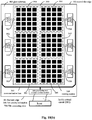
Fig. 10(a) illustrates a touch display apparatus according to the eighth embodiment of the present disclosure. This embodiment differs from the prior embodiments in that the display touch control chips arc provided at two or more chips and each of the chips is adapted to control a corresponding region of a display touch screen. - As an example, a common electrode layer is divided into multiple sub-regions. Each of the sub-regions includes multiple common electrodes arranged in a two-dimensional array and connected to one display touch control chip.
- Each of the display touch control chips may be clocked synchronously. Alternatively, the display touch control chips may operate in a time-sharing mode.
- As illustrated in
Fig. 10(a) , the common electrode layer includes multiple sub-regions 301-306, and each of the sub-regions includes multiple common electrodes. The shape of the common electrode is a square, a diamond or other polygon, or is a triangle, a circle or an ellipse. Moreover, some leeth may be provided at edges of the common electrode. For each of the sub-regions, the patterns of the common electrodes may be consistent or inconsistent. Preferably, the material of the common electrode is metal oxide such as indium tin oxide (ITO) or graphene, or is a conductive material such as a metal. - For each of the sub-regions, each of the common electrodes may be respectively connected to one of display touch control chips 1-6 corresponding to the common electrode through a wire. The display touch control chips 1-6 may be bound onto a first substrate or a second substrate in a COG mode.
- The display touch control chips 1-6 may be connected to a communication bus connecting terminal through a communication bus 700, and the communication bus connecting terminal may be connected to a host through a flexible printed
circuit 13. Preferably, the communication bus 700 is disposed in a non-transparent region except a sensing region, and may be a metal oxide line such as indium tin oxide (ITO) line or graphene line, and may also be a metal line. -
Fig. 10(b) illustrates another touch display apparatus according to the seventh embodiment of the present disclosure. This embodiment differs from the embodiment described inFig. 10(a) in that the driving sensing modules are provided at two or more chips and each of the modules is adapted to control a corresponding region of the display touch screen. - As an example, a common electrode layer is divided into multiple sub-regions. Each of the sub-regions includes multiple common electrodes arranged in a two-dimensional array and connected to one driving sensing module.
- The driving sensing modules may be clocked synchronously. Alternatively, the driving sensing modules may operate in a time-sharing mode.
- As illustrated in
Fig. 10(b) , the common electrode layer includes multiple sub-regions 301-306, and each of the sub-regions includes multiple common electrodes. The shape of the common electrode is a square, a diamond or other polygon, or is a triangle, a circle or an ellipse. Some teeth may be provided at edges of the common electrode. For each of the sub-regions, the patterns of the respective common electrodes may be consistent or inconsistent. Preferably, the material of the common electrode is metal oxide such as indium tin oxide (ITO) or graphene. - For each of the sub-regions, each of the common electrodes may he respectively connected to one of driving sensing modules 1-6 corresponding to the common electrode through a wire. The driving sensing modules 1-6 may be bound onto a substrate in a COG mode.
- The driving sensing modules 1-6 may be connected to a data processing and communication module through a communication bus 700, and the data processing and communication module may be connected to a host through a flexible printed
circuit 13. Preferably, the communication bus 700 is disposed in a non-transparent region except a sensing region, and may be a metal oxide line such as indium tin oxide (ITO) line or graphene line, and may also be a metal line. - The present embodiment is particularly suitable for a large-size screen. The two or more display touch control chips may scan a touch panel simultaneously. Therefore, a good image capture rate may be achieved.
- In the description, the emphasis is placed on difference between the embodiments. For the same or similar parts among the embodiments, they can be referred to from one another.
- The above description of the embodiments disclosed herein enables those skilled in the art to implement or use the present invention. Therefore, the present invention will not be limited to the embodiments described herein, but in accordance with the widest scope consistent with the principle and novel features disclosed herein.
Claims (15)
- A touch display apparatus, characterized comprising:a display touch screen comprising a first substrate (11, 21), a second substrate (13, 23), a liquid crystal layer (15, 25) and a plurality of pixel units, wherein each of the pixel units comprises a pixel electrode and wherein the liquid crystal layer (15, 25) and the pixel units are located between the first substrate and the second substrate, and the display touch screen further comprises a plurality of common electrodes (17, 1101-1120) arranged in a two-dimensional array, wherein the common electrodes (17, 1101-1120) are arranged so as to create in combination with the different pixel units an electric field across the liquid crystal material, so as to control luminuous flux of each pixel unit, anda display touch control circuit comprising a display control circuit and a touch control circuit, wherein the display touch control circuit is connected to the plurality of common electrodes (17, 1101-1120) through wires, and wherein the plurality of common electrodes (17, 1101-1120) are connected to a common level provided to the display control circuit during a phase of displaying, characterized in that each of the plurality of common electrodes (17, 1101-1120) is connected to the touch control circuit via an independent wire (501 - 520) as a touch sensing electrode during a phase of touch sensing.
- The touch display apparatus according to claim 1, wherein the wires (501-520) are disposed in a layer provided with the plurality of common electrodes (1101-1120), or the wires (501-503) are disposed in a layer different from a layer provided with the plurality of common electrodes and are connected to the plurality of common electrodes through via holes.
- The touch display apparatus according to claim 1, wherein the wires (501-520) are disposed in a layer provided with data lines, and are connected to the plurality of common electrodes (17, 1101-1120) through via holes.
- The touch display apparatus according to claim 1, wherein the wires (501-520) are disposed in a layer provided with the pixel electrodes and are connected to the plurality of common electrodes through via holes.
- The touch display apparatus according to claim 1, wherein the wires (501-520) are disposed right under a black matrix.
- The touch display apparatus according to claim 1, wherein the display touch control circuit (29) is a single chip, and the display control circuit and the touch control circuit are integrated in the single chip, the display touch control circuit comprises two or more chips, and the display control circuit and the touch control circuit are in different chips, or
the display touch control circuit comprises two or more chips, and each of the chips controls a part of the display touch screen; and optionally
wherein the chip for the display touch control circuit is bound onto the first substrate or the second substrate in chip-on-glass mode, or the chip for the display control circuit and the chip for the touch control circuit are bound onto the first substrate or the second substrate in chip-on-glass mode. - The touch display apparatus according to claim 1, wherein the touch control circuit is adapted to detect a self-capacitance of each of the common electrodes (17, 1101-1120); and optionally
wherein the touch control circuit is adapted to detect the self-capacitance of a current common electrode by a method comprising:driving, in response to a signal applied to the current common electrode, the current common electrode and common electrodes around the current common electrode simultaneously, ordriving, in response to a signal applied to the current common electrode, the current common electrode and all the other common electrodes simultaneously. - The touch display apparatus according to claim 7, wherein the touch control circuit is adapted to drive data lines simultaneously in response to the signal applied to the current common electrode.
- The touch display apparatus according to claim 7, wherein the touch control circuit is adapted to determine a touch position according to a two-dimensional capacitance sensing array.
- The touch display apparatus according to claim 1, wherein the display touch screen has an in-plane switching structure, a fringe field switching structure or a twisted nematic structure.
- The touch display apparatus according to claim 1, wherein the common electrode (17, 1101-1120) is in the shape of a regular polygon, the common electrode (17, 1101-1120) is in the shape of a rectangular, or the common electrode(17, 1101-1120) is in the shape of a circle, or the common electrode is in the shape of an ellipse.
- The touch display apparatus according to claim 1, wherein concave and convex structure is provided at edges of the common electrode (17, 1101-1120).
- The touch display apparatus according to claim 1, wherein the material of the plurality of common electrodes (17, 1101-1120) is indium tin oxide or grapheme; and optionally
wherein each of the pixel units of the display touch screen comprises a thin film transistor, the source of the thin film transistor is provided with a driving circuit adapted to drive the thin film transistor through a data line. - The touch display apparatus according to claim 1, wherein the touch display apparatus comprises a plurality of touch control circuits, and each of the touch control circuits is connected to corresponding common electrodes in the plurality of common electrodes (17, 1101-1120); and optionally
wherein the touch control circuits are clocked synchronously, or the touch control circuits operate in a time-sharing mode. - The touch display apparatus according to claim 1, wherein the display touch control circuit is adapted to execute repeatedly a first step comprising: performing a scan by the display control circuit and then performing a scan by the touch control circuit, or
the display touch control circuit is adapted to execute repeatedly a second step comprising: performing a scan by the touch control circuit and then performing a scan by the display control circuit; and optionally
wherein the display touch control circuit is configured to divide a frame scan performed by the display control circuit into a plurality of segments, and perform a scan by the touch control circuit every time before the frame scan, between the segments, and after the frame scan performed by the display control circuit.
Applications Claiming Priority (1)
| Application Number | Priority Date | Filing Date | Title |
|---|---|---|---|
| CN201310223963.3A CN103279245B (en) | 2013-06-06 | 2013-06-06 | Touch control display apparatus |
Publications (2)
| Publication Number | Publication Date |
|---|---|
| EP2811482A1 EP2811482A1 (en) | 2014-12-10 |
| EP2811482B1 true EP2811482B1 (en) | 2016-12-07 |
Family
ID=49061798
Family Applications (1)
| Application Number | Title | Priority Date | Filing Date |
|---|---|---|---|
| EP14152427.2A Active EP2811482B1 (en) | 2013-06-06 | 2014-01-24 | Touch liquid crystal display device |
Country Status (5)
| Country | Link |
|---|---|
| US (1) | US20140362031A1 (en) |
| EP (1) | EP2811482B1 (en) |
| JP (1) | JP5989018B2 (en) |
| KR (1) | KR101608794B1 (en) |
| CN (1) | CN103279245B (en) |
Families Citing this family (70)
| Publication number | Priority date | Publication date | Assignee | Title |
|---|---|---|---|---|
| CN103309535A (en) * | 2013-06-06 | 2013-09-18 | 敦泰科技有限公司 | Capacitive touch screen |
| CN103455201B (en) * | 2013-08-27 | 2017-03-29 | 北京京东方光电科技有限公司 | A kind of touch control display apparatus and its driving method |
| CN103472613A (en) * | 2013-09-13 | 2013-12-25 | 敦泰科技有限公司 | Capacitive touch display device |
| KR101641690B1 (en) * | 2013-09-25 | 2016-07-21 | 엘지디스플레이 주식회사 | Display device with integrated touch screen |
| CN104615291B (en) * | 2013-11-04 | 2017-12-08 | 凌巨科技股份有限公司 | Composite driving circuit for display touch panel |
| CN103713792B (en) * | 2013-12-23 | 2016-06-01 | 京东方科技集团股份有限公司 | Array substrate and manufacture method thereof and touch display unit |
| CN103926729B (en) * | 2013-12-31 | 2017-12-22 | 上海天马微电子有限公司 | Array substrate, color film substrate, touch display device and driving method thereof |
| CN103698927B (en) | 2013-12-31 | 2017-05-10 | 敦泰电子有限公司 | touch display device, drive circuit and drive method |
| CN103793120A (en) * | 2014-01-28 | 2014-05-14 | 北京京东方光电科技有限公司 | In cell touch panel and display device |
| CN104808826B (en) * | 2014-01-28 | 2018-06-15 | 晨星半导体股份有限公司 | Sensing electrode and sensing electrode unit |
| JP6375223B2 (en) * | 2014-01-31 | 2018-08-15 | 株式会社ジャパンディスプレイ | Display device with sensor and driving method thereof |
| US9557840B2 (en) * | 2014-02-04 | 2017-01-31 | Apple Inc. | Displays with intra-frame pause |
| CN104598085A (en) * | 2014-03-13 | 2015-05-06 | 北京智膜科技有限公司 | Touch screen control device and method based on intelligent film |
| US10564779B2 (en) * | 2014-04-25 | 2020-02-18 | Boe Technology Group Co., Ltd. | Array substrate and manufacturing method thereof, and touch display device |
| KR101696511B1 (en) * | 2014-05-19 | 2017-01-16 | 엘지디스플레이 주식회사 | Touch sensor integrated type liquid crystal display device |
| CN104020891A (en) | 2014-05-30 | 2014-09-03 | 京东方科技集团股份有限公司 | In cell touch panel and display device |
| CN104020893B (en) * | 2014-05-30 | 2017-01-04 | 京东方科技集团股份有限公司 | A kind of In-cell touch panel and display device |
| CN104020905B (en) | 2014-05-30 | 2017-06-16 | 京东方科技集团股份有限公司 | A kind of In-cell touch panel and display device |
| CN104020910B (en) * | 2014-05-30 | 2017-12-15 | 京东方科技集团股份有限公司 | A kind of In-cell touch panel and display device |
| CN104035640B (en) * | 2014-05-30 | 2017-10-27 | 京东方科技集团股份有限公司 | A kind of In-cell touch panel and display device |
| CN104022128B (en) * | 2014-05-30 | 2017-02-15 | 京东方科技集团股份有限公司 | Array substrate, manufacturing method thereof and displaying device |
| CN104020907B (en) * | 2014-05-30 | 2017-02-15 | 京东方科技集团股份有限公司 | In cell touch panel and display device |
| CN104020906B (en) * | 2014-05-30 | 2016-09-07 | 京东方科技集团股份有限公司 | A kind of In-cell touch panel and display device |
| CN104020909B (en) * | 2014-05-30 | 2017-06-30 | 京东方科技集团股份有限公司 | A kind of In-cell touch panel and display device |
| CN104020911A (en) | 2014-05-30 | 2014-09-03 | 京东方科技集团股份有限公司 | In cell touch panel and display device |
| CN104123039B (en) * | 2014-07-10 | 2017-08-01 | 京东方科技集团股份有限公司 | A kind of embedded touch display device and its driving method |
| CN104142772B (en) | 2014-07-24 | 2017-05-03 | 京东方科技集团股份有限公司 | Embedded type touch screen and display device |
| KR101597522B1 (en) * | 2014-08-28 | 2016-02-25 | 주식회사 지2터치 | The Touch Panel To Minimize Signal Distortion And, Display Apparatus Including The Same |
| US10209834B2 (en) | 2014-10-01 | 2019-02-19 | Microsoft Technology Licensing, Llc | Integrated self-capacitive touch display |
| CN104460080A (en) * | 2014-12-04 | 2015-03-25 | 深圳市华星光电技术有限公司 | Touch-control display device |
| CN104484068B (en) * | 2014-12-09 | 2018-09-18 | 深圳市华星光电技术有限公司 | A kind of embedded display screen, terminal and touch detecting method with touch function |
| CN104503172A (en) * | 2014-12-19 | 2015-04-08 | 深圳市华星光电技术有限公司 | Array substrate and display device |
| US9703439B2 (en) * | 2014-12-26 | 2017-07-11 | Lg Display Co., Ltd. | Touch sensor integrated type display device |
| CN104536609B (en) * | 2014-12-30 | 2018-01-30 | 深圳市华星光电技术有限公司 | Display panel and fault detection method with touch controllable function |
| JP6765807B2 (en) * | 2015-01-05 | 2020-10-07 | シナプティクス インコーポレイテッド | Modulation of reference voltage for capacitive sensing |
| KR102382999B1 (en) | 2015-01-08 | 2022-04-05 | 삼성디스플레이 주식회사 | Display device including touch sensor |
| CN108196725B (en) * | 2015-04-01 | 2021-02-02 | 上海天马微电子有限公司 | Touch display substrate and touch display device |
| CN104699322B (en) * | 2015-04-01 | 2017-12-29 | 上海天马微电子有限公司 | Array substrate, touch display panel, touch display device and detection method |
| CN104699354B (en) | 2015-04-01 | 2017-12-22 | 上海天马微电子有限公司 | Touch panel, driving method thereof and touch display device |
| CN107765488B (en) * | 2015-04-01 | 2019-12-31 | 上海天马微电子有限公司 | Array substrate, touch display panel and touch display device |
| CN104698711B (en) * | 2015-04-01 | 2018-06-01 | 上海天马微电子有限公司 | Array substrate, display panel and electronic equipment |
| CN104765501B (en) * | 2015-04-23 | 2018-01-23 | 厦门天马微电子有限公司 | Touch-control display panel, device and its driving method |
| CN104808858B (en) | 2015-05-08 | 2018-07-10 | 厦门天马微电子有限公司 | A kind of touch panel and touch control display apparatus |
| CN104793827B (en) * | 2015-05-08 | 2018-03-27 | 厦门天马微电子有限公司 | A kind of array base palte and self-capacitance touch control display apparatus |
| TWI628566B (en) * | 2015-05-28 | 2018-07-01 | 鴻海精密工業股份有限公司 | In-cell touch display panel |
| CN104866158B (en) * | 2015-06-18 | 2017-12-15 | 京东方科技集团股份有限公司 | A kind of In-cell touch panel and display device |
| CN106325618A (en) * | 2015-06-18 | 2017-01-11 | 宸鸿光电科技股份有限公司 | Touch panel |
| CN104866161B (en) * | 2015-06-23 | 2017-10-27 | 京东方科技集团股份有限公司 | A kind of In-cell touch panel and display device |
| CN104951162B (en) * | 2015-07-08 | 2019-01-22 | 京东方科技集团股份有限公司 | Touch display panel and driving method |
| CN105159486A (en) * | 2015-07-14 | 2015-12-16 | 京东方科技集团股份有限公司 | ADS array substrate, manufacturing method for ADS array substrate and display device |
| CN104965628B (en) * | 2015-07-17 | 2018-03-23 | 合肥京东方光电科技有限公司 | Capacitance type touch control substrate and touching display screen |
| CN105093721B (en) * | 2015-08-10 | 2018-03-13 | 上海天马微电子有限公司 | Touch display substrate, electronic equipment and driving method |
| CN105183259B (en) * | 2015-09-30 | 2018-11-02 | 上海天马微电子有限公司 | Touch panel and touch electronic equipment |
| CN105301822B (en) | 2015-12-11 | 2018-10-23 | 上海中航光电子有限公司 | A kind of array substrate, display panel and display device |
| CN105718115B (en) * | 2016-01-27 | 2019-05-21 | 上海天马微电子有限公司 | Touch display panel and display device |
| CN105677125B (en) * | 2016-02-04 | 2018-09-14 | 厦门天马微电子有限公司 | The modification method and display panel of a kind of display panel and its touching signals amount |
| JP6588852B2 (en) * | 2016-03-28 | 2019-10-09 | 株式会社ジャパンディスプレイ | Sensor and display device with sensor |
| CN105717690A (en) * | 2016-04-27 | 2016-06-29 | 武汉华星光电技术有限公司 | Embedded touch screen, preparation method thereof and liquid crystal display |
| KR101792524B1 (en) * | 2016-06-28 | 2017-11-02 | 주식회사 하이딥 | Touch input depvice |
| CN106959556B (en) * | 2016-09-27 | 2019-09-20 | 关键禾芯科技股份有限公司 | Liquid crystal module with fingerprint identification function |
| US20180323239A1 (en) * | 2017-05-03 | 2018-11-08 | Innolux Corporation | Display device |
| CN107132685B (en) * | 2017-06-23 | 2020-04-17 | 厦门天马微电子有限公司 | Display substrate, display panel and display device |
| US11403983B2 (en) | 2019-09-02 | 2022-08-02 | Samsung Electronics Co., Ltd. | Display controller, display system including the display controller, and method of operating the display controller |
| CN110738973A (en) * | 2019-09-09 | 2020-01-31 | 福建华佳彩有限公司 | panel driving method |
| CN110570752B (en) * | 2019-09-11 | 2021-11-02 | Oppo广东移动通信有限公司 | A display screen, electronic equipment and control method thereof |
| CN110794988B (en) * | 2019-10-22 | 2021-12-03 | 维沃移动通信有限公司 | Display module assembly and electronic equipment |
| CN117032486A (en) | 2020-02-14 | 2023-11-10 | 华为技术有限公司 | Display panels and display devices |
| CN114625329A (en) * | 2020-12-11 | 2022-06-14 | 慧荣科技股份有限公司 | Multi-screen display control device |
| CN114625330A (en) | 2020-12-11 | 2022-06-14 | 慧荣科技股份有限公司 | Multi-screen display control device |
| US11861098B2 (en) * | 2021-06-07 | 2024-01-02 | Wuhan China Star Optoelectronics Semiconductor Display Technology Co., Ltd. | Touch display panel |
Family Cites Families (16)
| Publication number | Priority date | Publication date | Assignee | Title |
|---|---|---|---|---|
| GB0208655D0 (en) * | 2002-04-16 | 2002-05-29 | Koninkl Philips Electronics Nv | Electronic device with display panel and user input function |
| US8040326B2 (en) * | 2007-06-13 | 2011-10-18 | Apple Inc. | Integrated in-plane switching display and touch sensor |
| JP4816668B2 (en) * | 2008-03-28 | 2011-11-16 | ソニー株式会社 | Display device with touch sensor |
| JP4996531B2 (en) * | 2008-04-23 | 2012-08-08 | 富士通コンポーネント株式会社 | Coordinate detection device |
| US8638314B2 (en) * | 2008-10-17 | 2014-01-28 | Atmel Corporation | Capacitive touch buttons combined with electroluminescent lighting |
| JP5249806B2 (en) * | 2009-02-16 | 2013-07-31 | グンゼ株式会社 | Touch switch |
| JP2010198615A (en) * | 2009-02-20 | 2010-09-09 | Acrosense Technology Co Ltd | Capacitive touch panel |
| CN101957507B (en) * | 2009-07-13 | 2012-10-17 | 上海天马微电子有限公司 | Touch screen liquid crystal display module and touch driving method thereof |
| US8390582B2 (en) * | 2009-08-25 | 2013-03-05 | Apple Inc. | Integrated touch screen |
| CN102109690B (en) * | 2009-12-25 | 2012-12-19 | 上海天马微电子有限公司 | Liquid crystal display device with embedded touch screen and control method |
| JP2012059073A (en) * | 2010-09-09 | 2012-03-22 | Bridgestone Corp | Information display device |
| EP2492784B1 (en) * | 2011-02-25 | 2021-02-24 | LG Display Co., Ltd. | Touch sensor integrated display device |
| US9760195B2 (en) * | 2011-09-23 | 2017-09-12 | Apple Inc. | Power management for integrated touch screens |
| JP2013097469A (en) * | 2011-10-28 | 2013-05-20 | Sharp Corp | Touch panel driving device, display device, touch panel driving method, program, and recording medium |
| CN103123548B (en) * | 2011-11-18 | 2016-12-07 | 宸鸿科技(厦门)有限公司 | touch display device |
| CN203376696U (en) * | 2013-06-06 | 2014-01-01 | 敦泰科技有限公司 | Touch control display device |
-
2013
- 2013-06-06 CN CN201310223963.3A patent/CN103279245B/en not_active Ceased
- 2013-11-18 US US14/083,223 patent/US20140362031A1/en not_active Abandoned
-
2014
- 2014-01-24 EP EP14152427.2A patent/EP2811482B1/en active Active
- 2014-02-03 KR KR1020140012304A patent/KR101608794B1/en active Active
- 2014-02-07 JP JP2014022336A patent/JP5989018B2/en active Active
Non-Patent Citations (1)
| Title |
|---|
| None * |
Also Published As
| Publication number | Publication date |
|---|---|
| JP5989018B2 (en) | 2016-09-07 |
| CN103279245A (en) | 2013-09-04 |
| EP2811482A1 (en) | 2014-12-10 |
| KR20140143314A (en) | 2014-12-16 |
| KR101608794B1 (en) | 2016-04-04 |
| US20140362031A1 (en) | 2014-12-11 |
| CN103279245B (en) | 2017-03-15 |
| JP2014238816A (en) | 2014-12-18 |
Similar Documents
| Publication | Publication Date | Title |
|---|---|---|
| EP2811482B1 (en) | Touch liquid crystal display device | |
| US9189117B2 (en) | Touch display device | |
| CN103226423B (en) | Embedded capacitive touch control display panel, display device, control device and method | |
| US10409416B2 (en) | Array substrate, color filter substrate, touch control display device and methods for driving the same | |
| KR102008779B1 (en) | Display Device With Integrated Touch Screen and Method for Driving The Same | |
| US7995041B2 (en) | Integrated touch screen | |
| US20140362029A1 (en) | Touch display apparatus | |
| US8217913B2 (en) | Integrated touch screen | |
| CN104049799B (en) | A kind of array base palte, In-cell touch panel and display device | |
| CN102221945B (en) | Touch screen, liquid crystal display and drive detection method | |
| CN203376696U (en) | Touch control display device | |
| CN103500044B (en) | Touch display panel and touch display unit | |
| US20140132534A1 (en) | Display Device Integrated with Touch Screen | |
| KR20150103659A (en) | In-cell touch panel and display device | |
| TW201500991A (en) | Touch display device | |
| KR102230843B1 (en) | In Cell Touch Liquid Crystal Display Device | |
| CN203455825U (en) | Touch display panel and touch display device | |
| TWI662461B (en) | Touch control apparatus | |
| TWI502430B (en) | Touch control apparatus | |
| CN104461120B (en) | It is integrated with the display device and its driving method of touch-screen |
Legal Events
| Date | Code | Title | Description |
|---|---|---|---|
| PUAI | Public reference made under article 153(3) epc to a published international application that has entered the european phase |
Free format text: ORIGINAL CODE: 0009012 |
|
| 17P | Request for examination filed |
Effective date: 20140124 |
|
| AK | Designated contracting states |
Kind code of ref document: A1 Designated state(s): AL AT BE BG CH CY CZ DE DK EE ES FI FR GB GR HR HU IE IS IT LI LT LU LV MC MK MT NL NO PL PT RO RS SE SI SK SM TR |
|
| AX | Request for extension of the european patent |
Extension state: BA ME |
|
| RAP1 | Party data changed (applicant data changed or rights of an application transferred) |
Owner name: FOCALTECH ELECTRONICS LTD. |
|
| RIC1 | Information provided on ipc code assigned before grant |
Ipc: G02F 1/1343 20060101ALN20160602BHEP Ipc: G06F 3/041 20060101ALN20160602BHEP Ipc: G09G 3/36 20060101AFI20160602BHEP Ipc: G06F 3/044 20060101ALN20160602BHEP |
|
| GRAP | Despatch of communication of intention to grant a patent |
Free format text: ORIGINAL CODE: EPIDOSNIGR1 |
|
| RIC1 | Information provided on ipc code assigned before grant |
Ipc: G06F 3/044 20060101ALN20160617BHEP Ipc: G06F 3/041 20060101ALN20160617BHEP Ipc: G09G 3/36 20060101AFI20160617BHEP Ipc: G02F 1/1343 20060101ALN20160617BHEP |
|
| RIC1 | Information provided on ipc code assigned before grant |
Ipc: G09G 3/36 20060101AFI20160630BHEP |
|
| RIN1 | Information on inventor provided before grant (corrected) |
Inventor name: MO, LIANGHUA Inventor name: OUYANG, GUANG |
|
| INTG | Intention to grant announced |
Effective date: 20160711 |
|
| GRAS | Grant fee paid |
Free format text: ORIGINAL CODE: EPIDOSNIGR3 |
|
| GRAA | (expected) grant |
Free format text: ORIGINAL CODE: 0009210 |
|
| AK | Designated contracting states |
Kind code of ref document: B1 Designated state(s): AL AT BE BG CH CY CZ DE DK EE ES FI FR GB GR HR HU IE IS IT LI LT LU LV MC MK MT NL NO PL PT RO RS SE SI SK SM TR |
|
| REG | Reference to a national code |
Ref country code: GB Ref legal event code: FG4D |
|
| REG | Reference to a national code |
Ref country code: CH Ref legal event code: EP Ref country code: AT Ref legal event code: REF Ref document number: 852347 Country of ref document: AT Kind code of ref document: T Effective date: 20161215 |
|
| REG | Reference to a national code |
Ref country code: IE Ref legal event code: FG4D |
|
| REG | Reference to a national code |
Ref country code: DE Ref legal event code: R096 Ref document number: 602014005260 Country of ref document: DE |
|
| PG25 | Lapsed in a contracting state [announced via postgrant information from national office to epo] |
Ref country code: LV Free format text: LAPSE BECAUSE OF FAILURE TO SUBMIT A TRANSLATION OF THE DESCRIPTION OR TO PAY THE FEE WITHIN THE PRESCRIBED TIME-LIMIT Effective date: 20161207 |
|
| REG | Reference to a national code |
Ref country code: LT Ref legal event code: MG4D |
|
| REG | Reference to a national code |
Ref country code: NL Ref legal event code: MP Effective date: 20161207 |
|
| PG25 | Lapsed in a contracting state [announced via postgrant information from national office to epo] |
Ref country code: NO Free format text: LAPSE BECAUSE OF FAILURE TO SUBMIT A TRANSLATION OF THE DESCRIPTION OR TO PAY THE FEE WITHIN THE PRESCRIBED TIME-LIMIT Effective date: 20170307 Ref country code: LT Free format text: LAPSE BECAUSE OF FAILURE TO SUBMIT A TRANSLATION OF THE DESCRIPTION OR TO PAY THE FEE WITHIN THE PRESCRIBED TIME-LIMIT Effective date: 20161207 Ref country code: SE Free format text: LAPSE BECAUSE OF FAILURE TO SUBMIT A TRANSLATION OF THE DESCRIPTION OR TO PAY THE FEE WITHIN THE PRESCRIBED TIME-LIMIT Effective date: 20161207 Ref country code: GR Free format text: LAPSE BECAUSE OF FAILURE TO SUBMIT A TRANSLATION OF THE DESCRIPTION OR TO PAY THE FEE WITHIN THE PRESCRIBED TIME-LIMIT Effective date: 20170308 |
|
| REG | Reference to a national code |
Ref country code: AT Ref legal event code: MK05 Ref document number: 852347 Country of ref document: AT Kind code of ref document: T Effective date: 20161207 |
|
| PG25 | Lapsed in a contracting state [announced via postgrant information from national office to epo] |
Ref country code: HR Free format text: LAPSE BECAUSE OF FAILURE TO SUBMIT A TRANSLATION OF THE DESCRIPTION OR TO PAY THE FEE WITHIN THE PRESCRIBED TIME-LIMIT Effective date: 20161207 Ref country code: ES Free format text: LAPSE BECAUSE OF FAILURE TO SUBMIT A TRANSLATION OF THE DESCRIPTION OR TO PAY THE FEE WITHIN THE PRESCRIBED TIME-LIMIT Effective date: 20161207 Ref country code: BE Free format text: LAPSE BECAUSE OF NON-PAYMENT OF DUE FEES Effective date: 20170131 Ref country code: RS Free format text: LAPSE BECAUSE OF FAILURE TO SUBMIT A TRANSLATION OF THE DESCRIPTION OR TO PAY THE FEE WITHIN THE PRESCRIBED TIME-LIMIT Effective date: 20161207 Ref country code: FI Free format text: LAPSE BECAUSE OF FAILURE TO SUBMIT A TRANSLATION OF THE DESCRIPTION OR TO PAY THE FEE WITHIN THE PRESCRIBED TIME-LIMIT Effective date: 20161207 |
|
| PG25 | Lapsed in a contracting state [announced via postgrant information from national office to epo] |
Ref country code: NL Free format text: LAPSE BECAUSE OF FAILURE TO SUBMIT A TRANSLATION OF THE DESCRIPTION OR TO PAY THE FEE WITHIN THE PRESCRIBED TIME-LIMIT Effective date: 20161207 |
|
| PG25 | Lapsed in a contracting state [announced via postgrant information from national office to epo] |
Ref country code: EE Free format text: LAPSE BECAUSE OF FAILURE TO SUBMIT A TRANSLATION OF THE DESCRIPTION OR TO PAY THE FEE WITHIN THE PRESCRIBED TIME-LIMIT Effective date: 20161207 Ref country code: SK Free format text: LAPSE BECAUSE OF FAILURE TO SUBMIT A TRANSLATION OF THE DESCRIPTION OR TO PAY THE FEE WITHIN THE PRESCRIBED TIME-LIMIT Effective date: 20161207 Ref country code: IS Free format text: LAPSE BECAUSE OF FAILURE TO SUBMIT A TRANSLATION OF THE DESCRIPTION OR TO PAY THE FEE WITHIN THE PRESCRIBED TIME-LIMIT Effective date: 20170407 Ref country code: RO Free format text: LAPSE BECAUSE OF FAILURE TO SUBMIT A TRANSLATION OF THE DESCRIPTION OR TO PAY THE FEE WITHIN THE PRESCRIBED TIME-LIMIT Effective date: 20161207 Ref country code: CZ Free format text: LAPSE BECAUSE OF FAILURE TO SUBMIT A TRANSLATION OF THE DESCRIPTION OR TO PAY THE FEE WITHIN THE PRESCRIBED TIME-LIMIT Effective date: 20161207 |
|
| PG25 | Lapsed in a contracting state [announced via postgrant information from national office to epo] |
Ref country code: BE Free format text: LAPSE BECAUSE OF FAILURE TO SUBMIT A TRANSLATION OF THE DESCRIPTION OR TO PAY THE FEE WITHIN THE PRESCRIBED TIME-LIMIT Effective date: 20161207 Ref country code: PT Free format text: LAPSE BECAUSE OF FAILURE TO SUBMIT A TRANSLATION OF THE DESCRIPTION OR TO PAY THE FEE WITHIN THE PRESCRIBED TIME-LIMIT Effective date: 20170407 Ref country code: PL Free format text: LAPSE BECAUSE OF FAILURE TO SUBMIT A TRANSLATION OF THE DESCRIPTION OR TO PAY THE FEE WITHIN THE PRESCRIBED TIME-LIMIT Effective date: 20161207 Ref country code: SM Free format text: LAPSE BECAUSE OF FAILURE TO SUBMIT A TRANSLATION OF THE DESCRIPTION OR TO PAY THE FEE WITHIN THE PRESCRIBED TIME-LIMIT Effective date: 20161207 Ref country code: BG Free format text: LAPSE BECAUSE OF FAILURE TO SUBMIT A TRANSLATION OF THE DESCRIPTION OR TO PAY THE FEE WITHIN THE PRESCRIBED TIME-LIMIT Effective date: 20170307 Ref country code: IT Free format text: LAPSE BECAUSE OF FAILURE TO SUBMIT A TRANSLATION OF THE DESCRIPTION OR TO PAY THE FEE WITHIN THE PRESCRIBED TIME-LIMIT Effective date: 20161207 Ref country code: AT Free format text: LAPSE BECAUSE OF FAILURE TO SUBMIT A TRANSLATION OF THE DESCRIPTION OR TO PAY THE FEE WITHIN THE PRESCRIBED TIME-LIMIT Effective date: 20161207 |
|
| REG | Reference to a national code |
Ref country code: CH Ref legal event code: PL |
|
| REG | Reference to a national code |
Ref country code: DE Ref legal event code: R097 Ref document number: 602014005260 Country of ref document: DE |
|
| PG25 | Lapsed in a contracting state [announced via postgrant information from national office to epo] |
Ref country code: MC Free format text: LAPSE BECAUSE OF FAILURE TO SUBMIT A TRANSLATION OF THE DESCRIPTION OR TO PAY THE FEE WITHIN THE PRESCRIBED TIME-LIMIT Effective date: 20161207 |
|
| PLBE | No opposition filed within time limit |
Free format text: ORIGINAL CODE: 0009261 |
|
| STAA | Information on the status of an ep patent application or granted ep patent |
Free format text: STATUS: NO OPPOSITION FILED WITHIN TIME LIMIT |
|
| REG | Reference to a national code |
Ref country code: FR Ref legal event code: ST Effective date: 20170929 |
|
| PG25 | Lapsed in a contracting state [announced via postgrant information from national office to epo] |
Ref country code: CH Free format text: LAPSE BECAUSE OF NON-PAYMENT OF DUE FEES Effective date: 20170131 Ref country code: FR Free format text: LAPSE BECAUSE OF NON-PAYMENT OF DUE FEES Effective date: 20170207 Ref country code: LI Free format text: LAPSE BECAUSE OF NON-PAYMENT OF DUE FEES Effective date: 20170131 |
|
| REG | Reference to a national code |
Ref country code: IE Ref legal event code: MM4A |
|
| 26N | No opposition filed |
Effective date: 20170908 |
|
| PG25 | Lapsed in a contracting state [announced via postgrant information from national office to epo] |
Ref country code: DK Free format text: LAPSE BECAUSE OF FAILURE TO SUBMIT A TRANSLATION OF THE DESCRIPTION OR TO PAY THE FEE WITHIN THE PRESCRIBED TIME-LIMIT Effective date: 20161207 Ref country code: SI Free format text: LAPSE BECAUSE OF FAILURE TO SUBMIT A TRANSLATION OF THE DESCRIPTION OR TO PAY THE FEE WITHIN THE PRESCRIBED TIME-LIMIT Effective date: 20161207 Ref country code: LU Free format text: LAPSE BECAUSE OF NON-PAYMENT OF DUE FEES Effective date: 20170124 |
|
| PG25 | Lapsed in a contracting state [announced via postgrant information from national office to epo] |
Ref country code: IE Free format text: LAPSE BECAUSE OF NON-PAYMENT OF DUE FEES Effective date: 20170124 |
|
| PG25 | Lapsed in a contracting state [announced via postgrant information from national office to epo] |
Ref country code: MT Free format text: LAPSE BECAUSE OF NON-PAYMENT OF DUE FEES Effective date: 20170124 |
|
| PG25 | Lapsed in a contracting state [announced via postgrant information from national office to epo] |
Ref country code: HU Free format text: LAPSE BECAUSE OF FAILURE TO SUBMIT A TRANSLATION OF THE DESCRIPTION OR TO PAY THE FEE WITHIN THE PRESCRIBED TIME-LIMIT; INVALID AB INITIO Effective date: 20140124 |
|
| PG25 | Lapsed in a contracting state [announced via postgrant information from national office to epo] |
Ref country code: CY Free format text: LAPSE BECAUSE OF FAILURE TO SUBMIT A TRANSLATION OF THE DESCRIPTION OR TO PAY THE FEE WITHIN THE PRESCRIBED TIME-LIMIT Effective date: 20161207 |
|
| PG25 | Lapsed in a contracting state [announced via postgrant information from national office to epo] |
Ref country code: MK Free format text: LAPSE BECAUSE OF FAILURE TO SUBMIT A TRANSLATION OF THE DESCRIPTION OR TO PAY THE FEE WITHIN THE PRESCRIBED TIME-LIMIT Effective date: 20161207 |
|
| PG25 | Lapsed in a contracting state [announced via postgrant information from national office to epo] |
Ref country code: TR Free format text: LAPSE BECAUSE OF FAILURE TO SUBMIT A TRANSLATION OF THE DESCRIPTION OR TO PAY THE FEE WITHIN THE PRESCRIBED TIME-LIMIT Effective date: 20161207 |
|
| PG25 | Lapsed in a contracting state [announced via postgrant information from national office to epo] |
Ref country code: AL Free format text: LAPSE BECAUSE OF FAILURE TO SUBMIT A TRANSLATION OF THE DESCRIPTION OR TO PAY THE FEE WITHIN THE PRESCRIBED TIME-LIMIT Effective date: 20161207 |
|
| P01 | Opt-out of the competence of the unified patent court (upc) registered |
Effective date: 20230526 |
|
| PGFP | Annual fee paid to national office [announced via postgrant information from national office to epo] |
Ref country code: DE Payment date: 20250129 Year of fee payment: 12 |
|
| PGFP | Annual fee paid to national office [announced via postgrant information from national office to epo] |
Ref country code: GB Payment date: 20250127 Year of fee payment: 12 |