EP2811453B1 - Visuelle kortexschaltvorrichtung - Google Patents
Visuelle kortexschaltvorrichtung Download PDFInfo
- Publication number
- EP2811453B1 EP2811453B1 EP13740808.4A EP13740808A EP2811453B1 EP 2811453 B1 EP2811453 B1 EP 2811453B1 EP 13740808 A EP13740808 A EP 13740808A EP 2811453 B1 EP2811453 B1 EP 2811453B1
- Authority
- EP
- European Patent Office
- Prior art keywords
- unit
- current
- voltage
- visual cortical
- circuit apparatus
- Prior art date
- Legal status (The legal status is an assumption and is not a legal conclusion. Google has not performed a legal analysis and makes no representation as to the accuracy of the status listed.)
- Active
Links
Images






Classifications
-
- G—PHYSICS
- G06—COMPUTING OR CALCULATING; COUNTING
- G06N—COMPUTING ARRANGEMENTS BASED ON SPECIFIC COMPUTATIONAL MODELS
- G06N3/00—Computing arrangements based on biological models
- G06N3/02—Neural networks
- G06N3/04—Architecture, e.g. interconnection topology
-
- G—PHYSICS
- G06—COMPUTING OR CALCULATING; COUNTING
- G06F—ELECTRIC DIGITAL DATA PROCESSING
- G06F16/00—Information retrieval; Database structures therefor; File system structures therefor
- G06F16/50—Information retrieval; Database structures therefor; File system structures therefor of still image data
- G06F16/58—Retrieval characterised by using metadata, e.g. metadata not derived from the content or metadata generated manually
- G06F16/583—Retrieval characterised by using metadata, e.g. metadata not derived from the content or metadata generated manually using metadata automatically derived from the content
-
- G—PHYSICS
- G06—COMPUTING OR CALCULATING; COUNTING
- G06F—ELECTRIC DIGITAL DATA PROCESSING
- G06F18/00—Pattern recognition
- G06F18/20—Analysing
- G06F18/21—Design or setup of recognition systems or techniques; Extraction of features in feature space; Blind source separation
-
- G—PHYSICS
- G06—COMPUTING OR CALCULATING; COUNTING
- G06N—COMPUTING ARRANGEMENTS BASED ON SPECIFIC COMPUTATIONAL MODELS
- G06N3/00—Computing arrangements based on biological models
- G06N3/02—Neural networks
- G06N3/04—Architecture, e.g. interconnection topology
- G06N3/0464—Convolutional networks [CNN, ConvNet]
-
- G—PHYSICS
- G06—COMPUTING OR CALCULATING; COUNTING
- G06N—COMPUTING ARRANGEMENTS BASED ON SPECIFIC COMPUTATIONAL MODELS
- G06N3/00—Computing arrangements based on biological models
- G06N3/02—Neural networks
- G06N3/06—Physical realisation, i.e. hardware implementation of neural networks, neurons or parts of neurons
- G06N3/063—Physical realisation, i.e. hardware implementation of neural networks, neurons or parts of neurons using electronic means
- G06N3/065—Analogue means
-
- G—PHYSICS
- G06—COMPUTING OR CALCULATING; COUNTING
- G06T—IMAGE DATA PROCESSING OR GENERATION, IN GENERAL
- G06T1/00—General purpose image data processing
- G06T1/20—Processor architectures; Processor configuration, e.g. pipelining
-
- G—PHYSICS
- G06—COMPUTING OR CALCULATING; COUNTING
- G06V—IMAGE OR VIDEO RECOGNITION OR UNDERSTANDING
- G06V10/00—Arrangements for image or video recognition or understanding
- G06V10/40—Extraction of image or video features
- G06V10/44—Local feature extraction by analysis of parts of the pattern, e.g. by detecting edges, contours, loops, corners, strokes or intersections; Connectivity analysis, e.g. of connected components
- G06V10/443—Local feature extraction by analysis of parts of the pattern, e.g. by detecting edges, contours, loops, corners, strokes or intersections; Connectivity analysis, e.g. of connected components by matching or filtering
- G06V10/449—Biologically inspired filters, e.g. difference of Gaussians [DoG] or Gabor filters
-
- G—PHYSICS
- G06—COMPUTING OR CALCULATING; COUNTING
- G06V—IMAGE OR VIDEO RECOGNITION OR UNDERSTANDING
- G06V10/00—Arrangements for image or video recognition or understanding
- G06V10/94—Hardware or software architectures specially adapted for image or video understanding
- G06V10/955—Hardware or software architectures specially adapted for image or video understanding using specific electronic processors
Definitions
- the present invention relates to a visual cortical circuit apparatus.
- Recent technological advancements in systems neuroscience have allowed for the recognition of an object from an image, based on input and output patterns of cells constituting a visual system and the signal processing method of cells.
- a neural network such as a semiconductor chip, which is designed to have a response similar to that of the human brain or neurons, has been designed so that the network connects a large number of simple elements through communication and thereby expresses and memorizes information.
- the neural network made by imitating the structure of a neuron in the neural network of a human brain, is used as a core technology in artificial intelligence computers in areas of voice recognition, character recognition, image processing and understanding of natural language, and is being actively researched in many countries.
- the Korean publicized patent No. 2006-0089487 which deals with an apparatus for compensating images according to probabilistic neural network theory, discloses an apparatus that can provide a user with a high-quality image.
- the patent does not disclose a technique that can have the same precision as an optic nerve and miniaturize the apparatus.
- GB2416236 describes a signal processing circuit such as an arithmetic circuit for performing arithmetic operations such as multiplication and/or addition/subtraction and a circuit having a voltage-controlled transconductance has a first MOSFET arrangement M1,M2,M3,M4 for performing an arithmetic operation for given first operands VIN, VC and, preferably, at least one other MOSFET M5 for performing substantially the same arithmetic operation for given second operands with the second operands being chosen to influence the output of the first MOSFET circuit by at least reducing, and preferably, eliminating, the presence of an undesirable component of the output of the first MOSFET circuit.
- US 6507828 B1 describes a neuron circuit including means for synaptic Korea Institute of Science and Technology, Application No.: 13 740 808.4-1906 17.07.2018 modification.
- the circuit emulates the electrical behaviors of the neuron membrane, dendrite, and synapse, using principles based on the actual biology.
- the circuit is implemented as an analog very large scale integrated (VLSI) circuit which utilizes CMOS integrated circuit technology.
- VLSI very large scale integrated
- the analog VLSI circuit includes a synapse circuit having a circuit portion which models a mechanism for the modification of the synaptic conductance.
- An object of some embodiments of the present invention is to provide a visual cortical circuit apparatus that can offer a parallel structure implementable in the form of a small chip even when an object is located in unfavorable conditions, thus leading to a sharp increase in the number of visual cortical circuit apparatuses required for detecting the object, and an apparatus and a method for providing rescue information using the visual cortical circuit apparatus.
- a visual cortical circuit apparatus comprises: a current mirror unit for using a transistor as a current source to generate a current having the same magnitude as that of a reaction; a transconductance unit for receiving, as an input, the current generated by the current mirror unit and outputting a voltage using transconductance; and a buffer unit for converting the voltage output by the transconductance unit into a current and buffering the current.
- a visual cortical imitation system using the visual cortical circuit apparatus comprises: a bias unit for applying a bias voltage to maintain a reference operating point when a magnitude of a reaction output by the visual cortical circuit apparatus over neuron response time is less than a predetermined threshold value; a current mirror unit for using a transistor as a current source to generate a current having the same magnitude as the current inputted by the bias unit; a transconductance unit for receiving, as an input, the current generated by the current mirror unit and outputting a voltage using transconductance; a buffer unit for converting the voltage output by the transconductance unit into a current and buffering the current; and a bipolar switching unit, wherein any one of outputs from the buffer unit is switched on if a membrane potential proceeds across a neuron so that the neuron becomes activated, and switched off if a membrane potential proceeds across a neuron so that the neuron becomes deactivated.
- a visual cortical circuit apparatus comprises: a transconductance unit for taking, as an input, a value with an offset applied to distinguish between the background of an image or picture and an object to be searched for; an externally-controlled voltage application unit for setting an offset; and a buffer unit for applying a weight by amplifying an input voltage or input current for the same frame as the pattern of the object.
- An object search system using a visual cortical circuit apparatus comprises: a conversion unit for converting an input image into a black-and-white image as a pre-treatment process to search for an object from an image or picture; a transconductance unit for receiving, as an input, a value with an offset applied to distinguish between the background of an image or picture and the object to be searched for; an externally-controlled voltage application unit for setting the offset; a buffer unit for applying a weight by amplifying an input voltage or input current for the same frame as the pattern of the object; and a search unit for singling out and detecting the object from an image with an offset and a weight applied.
- Any one of the technical solutions of the invention described above can provide a parallel structure implementable in the form of a small chip, even when an object is located in unfavorable conditions, thereby resulting in a sharp increase in the number of visual cortical circuit apparatuses required for detecting the object.
- connection of one portion to another includes the meaning of “electrical connection” of two portions having another element between the two, as well as “direct connection” between the two.
- a portion includes a component means that the portion can further include other components, rather than exclude other components, unless otherwise described, and should be understood in the sense that the possibility that one or more other features, numbers, steps, operations, components or parts, or the combinations thereof are present or can be added is not ruled out beforehand.
- a first and “a second” are used to distinguish one component from another and should not limit the scope of the rights to the invention.
- a first component can be called a second component, and vice versa.
- Reference numerals in each step are used for convenience in explanation, and do not refer to the sequence of steps. The steps can be performed in a different order from the stated one, unless a specific order is mentioned in the context. In other words, the steps can be performed in the same order as the stated one, effectively simultaneously, or in the reverse order.
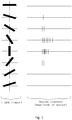
- FIG. 1 is a diagram of cerebral cortex response for describing the concept of a visual cortical circuit apparatus according to an embodiment of the invention
- FIG. 2 is a graph of a response to stimuli for describing the concept of a visual cortical circuit apparatus according to an embodiment of the invention.
- FIG. 1 shows a response of a cat's cerebral cortex when light with directionality is cast on the cat's eyes.
- neurons of the cat's cerebral cortex come to have specific directionality and respond to stimuli in a specific direction.
- the left of FIG. 1 illustrates the shape or direction of the light, and the diagram on the right shows the magnitude of the response to the shape or direction of the light.
- a brain is a set of neurons giving an independent stimulus to a specific directionality.
- a circuit implemented by imitating a visual cell yields precision similar to that of visual cortex.
- a neuron's response to stimuli over time can be expressed in a voltage and transconductance.
- Vm-g voltage and transconductance
- transconductance is the real component of transadmittance and is also called mutual conductance.
- FIG. 3 illustrates a transistor and an equivalent circuit thereof for describing the concept of a transistor according to an embodiment of the invention.
- a transistor can have a non-linear characteristic equivalent model for resistance or conductance.
- the FET Field Effect Transistor
- the FET may be a voltage control type, which controls electron flow in a semiconductor with another electrode.
- MOSFET Metal Oxide Silicon Field Effect Transistor
- resistance or conductance having a current non-linearly proportional to an applied voltage. This can be shown by referring to the voltage-current characteristic graph of V DS and i D (voltage-current characteristic graph for N-channel MOSFET).
- the N-channel MOSFET is taken as an example, the same principle also applies to the P-channel MOSFET. Since the P-channel MOSFET has the same circuit device structure except for the variation in accordance with the channel polarities of the transistor, it is obvious that the P-channel MOSFET can also be used to structure the circuit device.
- the current-voltage relationship of the N-channel MOSFET in the triode region in FIG. 3 may be non-linear as can be seen in the Mathematical Equation 1 below because the current involves a second order voltage V DS .
- I DS K V GS ⁇ V T V DS ⁇ V 2 DS 2
- K ⁇ C OX W 2 ⁇ L
- V T is an individual parameter variable in accordance with the MOSFET manufacturing
- I DS is a drain-source current
- V GS is a gate-source voltage
- V DS is a drain-source voltage
- L refers to the length between source and drain of the MOSFET
- W is the width of the MOSFET.
- FIG. 4 is a circuit diagram for describing a visual cortical circuit apparatus according to an embodiment of the invention.
- the visual cortical circuit apparatus 100 contains a current mirror unit 110, a transconductance unit 130 and a buffer unit 150.
- the current mirror unit 110 uses a transistor as a current source to generate a current having the same magnitude as that of a reaction.
- the visual cortical circuit apparatus 100 is a symmetrical operational amplifier, and the operational amplifier may be an analog operational amplifier. Therefore, the current mirror unit 110 comprises at least one current mirror, and the at least one current mirror is connected in parallel in up/down symmetry.
- the current mirror unit 110 may contain a first current mirror having N-channel MOSFETs M1 and M2 and a second current mirror having P-channel MOSFETs M3 and M4.
- the current source signal input is transmitted to the transconductance unit 130 through the first current mirror and the second current mirror.
- the current mirror is a circuit designed to duplicate a current through one active element by controlling the current of another active element in the circuit in order to maintain a certain level of output current, regardless of the load.
- the current can be duplicated and may be one of various signal currents.
- the current mirror may provide an active load for a bias current and a circuit.
- the transconductance unit 130 receives, as an input, the current generated by the current mirror unit 110 and outputs a voltage using transconductance.
- the visual cortical circuit apparatus 100 is a symmetrical operational amplifier, and the transconductance unit 130 may be an equivalent circuit of a differential transconductance amplifier.
- the transconductance unit 130 contains at least one transconductance circuit and the at least one trandsconductance circuit is connected in parallel in up/down symmetry.
- the transconductance circuit of the transconductance unit 130 may comprise P-channel MOSFET M5 and N-channel MOSFETs M6 and M7.
- the transconductance unit 130 may control the properties of a terminal with a voltage applied to the gate of M7 and output a voltage by multiplying by the current source input signal.
- V D is a fixed constant and I and V X are signals. Both of K and V con are fixed constants.
- the MOSFETs M5, M6 and M7 may have the characteristics of voltage-controlled linear resistance or conductance, and since the result of the multiplication of the current source input signal and the resistance can be expressed as V x or the drain voltage of M6 and M7, the current source input signal can be presented as a voltage.
- the buffer unit 150 converts the voltage output by the transconductance unit 130 into a current and buffer the current.
- the buffer may be a separated device or reaction absorption device that is disposed between a driving device and a driven device in order to prevent the driving device from receiving a reaction from the driven device.
- the buffer unit 150 has a high input impedance and a low output impedance, and may prevent a counter flow of the current.
- the visual cortical circuit apparatus 100 is a symmetrical operational amplifier, the buffer unit 150 contains at least one buffer circuit and the at least one buffer circuit is connected in parallel in up/down symmetry.
- the parallel connection of the at least one visual cortical circuit apparatus 100 may allow the designing of VLSI with the capability of complex operations.
- the visual cortical circuit apparatus 100 may be connected to another in a parallel or serial fashion or a combination thereof, and may comprise at least one or at least one combination of BJT (Bipolar Junction Transistor), JFET (Junction Field-Effect Transistor), MOSFET (Metal-Oxide Semiconductor Field-Effect Transistor) and GaAs MESFET (Metal Semiconductor FET).
- BJT Bipolar Junction Transistor
- JFET Joint Field-Effect Transistor
- MOSFET Metal-Oxide Semiconductor Field-Effect Transistor
- GaAs MESFET Metal Semiconductor FET
- FIG. 5 is a circuit diagram for describing a visual cortical circuit apparatus further having a bias unit in the visual cortical circuit apparatus in FIG. 4 .
- the visual cortical circuit apparatus 100 according to an embodiment of the invention further contains a bias unit 170 for applying a bias voltage so that the current mirror unit 110 can remain in the operational state when the magnitude of a reaction is less than a predetermined threshold value.
- biasing means moving the operating point backward from the origin so that, with a voltage already applied in a forward direction, a current starts flowing as soon as a signal input occurs, since a signal input lower than a certain level does not cause the current to flow when a voltage is not applied between a base and an emitter in the transistor.
- the bias unit 170 is symmetrical, and the output current resulting from biasing may be eliminated in the buffer unit 150.
- the current mirror unit 110 may not operate in the normal operation region and therefore biasing is used. Therefore, only the first current source input signal can go through final operation processing by adding only the variation in the current source input signal within the minimum current range to the normal criteria for biasing.
- FIG. 6 is a circuit diagram for describing a visual cortical circuit apparatus further having a bipolar switch unit in the visual cortical circuit apparatus in FIG. 4 .
- the visual cortical circuit apparatus 100 according to an embodiment of the invention further contains a bipolar switch unit 190 for selectively switching a bipolar signal output.
- a visual cortical imitation system modeled on brain should be designed in such a way that more nerve stimuli should lead to the activation of new neurons and fewer nerve stimuli should lead to the deactivation of new neurons, in order to perform similar functions to those of the brain.
- the bipolar switch unit 190 switches on any one of outputs from the buffer unit 150 a membrane potential proceeds across a neuron so that the neuron becomes activated, and switches off any one of outputs from the buffer unit 150 a membrane potential proceeds across a neuron so that the neuron becomes deactivated.
- the switch MOSFET MO1 is turned on to make the upper end output of the visual cortical circuit apparatus 100 effective and, at the same time, the switch MOSFET MO2 is turned off to make the lower end output of the visual cortical circuit apparatus 100 ineffective.
- the MOSFET MO1 is turned off to make the lower end output of the visual cortical circuit apparatus 100 effective and, at the same time, the MOSFET MO2 is turned on.
- FIG. 7 is a diagram for describing a visual cortical imitation system using a visual cortical circuit apparatus according to an embodiment of the invention.
- FIG. 7 is also a schematic diagram of the neural network of visual cortex implemented using the visual cortical circuit apparatus 100 according to an embodiment of the invention.
- the output and connection of a single pixel sensor may be presented as the action in the bias unit 170, and multiple connections to many synapses and neurons may be presented as the combined action in the current mirror unit 110, the transconductance unit 130, the buffer unit 150 and the bipolar switching unit 190 (not shown).
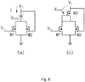
- FIG. 8 is a diagram for describing the concept of a transistor according to an example useful for understanding the invention.
- (a) represents transconductance in terms of a current I
- (b) represents transconductance in terms of a voltage V.
- the circuits (a) and (b) may comprise a linear conductance circuit whose voltage is controlled by a pair of NMOS (N Metal Oxide Semiconductor) transistors M1 and M2. This can be applied to various neural networks, from active synapses to neurons.
- NMOS N Metal Oxide Semiconductor
- FIG. 9 is a diagram for describing a visual cortical circuit apparatus according to an example useful for understanding the invention.
- a visual cortical circuit apparatus 200 contains a transconductance unit 210, an externally-controlled voltage application unit 220 and a buffer unit 240.
- the visual cortical circuit apparatus 200 may further contain a current mirror unit 230.
- the characteristics of a biological cell can be applied.
- one circuit may correspond to one neuron. Therefore, the chip made by connecting in parallel one or more of these circuits can perform functions similar to those of brain. However, modifications should be made to fit the voltage characteristics of a neuron and the characteristics of each connection between neurons should be considered.
- the visual cortical circuit apparatus 200 may present the response of a neuron in visual cortex to stimuli over time in the form of a voltage, and may output a voltage equivalent to the presented voltage. However, the visual cortical circuit apparatus 200 may have a visual cortical circuit representing a connection between neurons or between a neuron and a sensor, with a weighted synapse imposed therebetween, as in the neural network of the brain.
- the transconductance unit 210 can be implemented to imitate the action potential of biological neural cell and the characteristics of selective transconductance for each cell membrane ion. Also, the externally-controlled voltage application unit 220 may apply a voltage to the transconductance unit 210 in order to enable the further programming of the calculated current of the transconductance.
- the current mirror unit 230 may duplicate the output current from the transconductance unit 210 and prevent a counter flow by mirroring the output voltage from the transconductance unit 210.
- the buffer unit 240 can prevent a counter flow of voltage by buffering the output voltage fed back from the output stage.
- FIG. 10 is a circuit diagram for describing another example of the visual cortical circuit apparatus in FIG. 9 .
- the top and bottom may correspond to the Leakage portion and Na or K portion, respectively.
- the additional parallel connection between each portion may lead to the creation of N portions.
- Equation 5 the empirical mathematical formula of conductance elements is expressed by the Mathematical Equation 5, where b represents a sigmoid function of membrane potential.
- Vm refers to membrane potential and can be dynamically modeled on the whole by the conduction of active potential and relevant ions.
- Mathematical Equation 5 is controlled by conductance, multiplication, addition, subtraction and differential equation.
- the differential equation may be implemented by the LPF (Low Pass Filter) and may cause a delayed response.
- LPF Low Pass Filter
- a neuron may be understood to electrically behave as ion-based conductance controlled by membrane potential for the biologically dynamic action thereof.
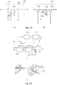
- FIG. 11 is a diagram for describing the concept of an offset applied to the visual cortical circuit apparatus in FIG. 9
- FIG. 12 is a diagram for conceptually illustrating the visual cortical circuit apparatus in FIG. 9 with an offset applied.
- the offset value is applied to the black-and-white image so that the pattern as an object can have a negative value.
- the offset is added to the pixel values for an area corresponding to the background, the offset is subtracted from the pixel values for an area corresponding to the object, and then a weight frame is applied.
- the background in the image comes to have a higher value, in comparison with the object to be searched for.
- the application of a positive value to the background and of a negative value to the target object leads to a wider gap between the two.
- the background can be expressed as dark and the object can be expressed as bright, thereby increasing selectivity.
- the offset depends on the type of the image or object.
- the offset can be set as the average of pixel values of the black-and-white image.
- the application of an offset before the application of a weight frame may correctly detect an object to avoid any noise or error.
- FIG. 13 is a circuit diagram of a switched capacitor unit added to the visual cortical circuit apparatus in FIG. 9 .
- the switched capacitor unit 300 may include a first switch 310, a capacitor 320, a second switch 330 and a third switch 340.
- the first switch 310 may allow output current from the buffer unit 200 to flow for a certain period of time.
- the electric charge (Q) stored in the capacitor 320 for the certain period of time (T on ), during which the first switch 310 is connected, is presented in the Mathematical Equation 6 below.
- the capacitor 320 is connected in parallel to the first switch 310 and may store the output current from the buffer unit 200 as electric charge. This is shown in the Mathematical Equation 6 above.
- the second switch 330 may be connected in parallel to the capacitor 320 and be connected in series to the first switch 310.
- the first switch 310 and the second switch 330 may have separate On/Off timing.
- the third switch 340 may discharge the residual charge of the capacitor 320 before the first switch 310 is electrically connected.
- the switched capacitor unit 300 can be implemented in the form of either (a) or (b) of FIG. 13 .
- the visual cortical circuit apparatus 200 To sum up the charge stored in the capacitor 320, the visual cortical circuit apparatus 200 should be connected in parallel, which is described with reference to FIG. 14 .
- FIG. 14 is a circuit diagram of the parallel connection of the visual cortical circuit apparatus in FIG. 9 .
- FIG. 14 an example of n visual cortical circuit apparatuses 200 connected in parallel is taken for explanation.
- the sum of the charges (Q) stored in each of the capacitors 320 is a total charge (Qtot), and the total charge divided by the multiplication of the number of capacitors 320 by the capacitance yields a total voltage. This can be inferred from a simple principle that for capacitors in parallel connection, the sum of each electric charge equals the total charge.
- the output voltage may be calculated based on the sum of electric charges stored in at least one switched capacitor 300.
- the visual cortical circuit apparatus 200 may further contain an integrated capacitor 500 and an integrated switch 600.
- the integrated switch 600 may be equipped in order to discharge the residual charge of the integrated capacitor 500 before the visual cortical circuit apparatus 200 is electrically connected.
- the addition of the integrated switch 600 may change the Mathematical Equation 7 above into the Mathematical Equation 8 below.
- V out Q tot nC + C o ⁇ V tot
- C 0 refers to the capacity of the integrated capacitor 500.
- the integrated capacitor 500 may prevent the output saturation caused by the interlocking of massive neural synapses, as well as sum the output voltages (V out ).
- the integrated capacitor 500 may have the same effect as the multiplication of a coefficient less than 1.
- the on-time of the second switch 330 of at least one visual cortical circuit apparatus 200 is necessary for charge redistribution, and therefore does not matter.
- the visual cortical circuit apparatus 200 has two parallel structures. Since an unlimited number of parallel structures, not just two, is possible due to the current-source basis, the operation requiring a structure of massive synapses can be implemented in a small chip.
- the switched capacitor unit 300 is necessary because the interlocking of 1,500 to 2,000 synapses per neuron may be required in unfavorable conditions for searching for an object.
- the directional operation an early visual intelligence phase of brain, may require the interlocking of 100 to 200 synapses on a relatively small scale. These conditions may serve as a constraint in the miniaturization of semiconductor chips or the implementation of VLSI or imbedded systems.
- the switched capacitor unit 300 can solve the problem of the interlocking of massive synapses and meet the criteria for miniaturization by using the fact that the neuronal activation degree is determined by the accumulation of positive/negative currents transmitted from the synapses.
- the switched capacitor unit 300 may store the current source, which is the result of the operation by synapses split in a certain unit, in each capacitor in the form of an electric charge, and then connect all capacitors for the whole operation, thereby meeting the criteria for miniaturization.
- the use of the switched capacitor unit 300 can solve the problem of the interlocking of massive synapses and miniaturize semiconductor chips, which is required in unfavorable conditions.
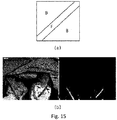
- FIG. 15 illustrates an example of searching for an object using the visual cortical circuit apparatus in FIG. 9 .
- F is defined as an object and B is defined as the background.
- an offset and weight applied to the object and background are expressed by the Mathematical Equation 9 below.
- F ⁇ weight input
- B ⁇ weight input
- the Mathematical Equation 9 shows that only weight is applied to input for the background (B), while the offset is subtracted from input before multiplying by weight for the object, as a pattern to be detected and searched for.
- the subtraction of the offset is followed by the multiplication of the weight
- the addition of the offset is followed by the multiplication of the weight, thereby widening the gap. Accordingly, the input image on the left is converted into the input image on the right, and the seat belt, as an object, is detected as white.
- FIG. 16 illustrates an example of generating rescue information using the visual cortical circuit apparatus in FIG. 9
- FIG. 17 is an example implementation of generating rescue information from an image, using the visual cortical circuit apparatus in FIG. 9 .
- the rescue information is generated by graphic-processing the shape of the object in order to protect the personal information of the passenger.
- visual processing may allow the position of the head and the posture and slope of the upper body to be recognized and the working of the airbag and the wearing of the seat belt to be checked.
- the object is a person
- the person can be graphic-processed.
- the personal information of the passenger to be transmitted may be summarized into the position of the seat, the slope as the posture of the upper body, the position of the head, etc. Since the rescue center can determine the damage by the symbolized graphic alone, the personal information, which could be sensitive information, can be protected fundamentally. Also, since the amount of information transmitted to the rescue center can be minimized, the transmission speed can increase.
- (b) represents a case in which the rescue information is generated in the form of a text or multimedia message (SMS/MMS).
- SMS/MMS text or multimedia message
- FIG. 17 illustrates a clear screenshot of the rescue information, wherein the detected image is converted into a black-and-white image; the background and the object are separated by applying an offset and a weight to the image; the position and slope of the object are identified; and then the information goes through graphic-processing if the object is a person.
- the capability of the directional operation to imitate the visual cortical circuit can be improved through the extraction of the characteristics of the visual information.
- the improvement of the result of the directional operation can improve the object recognition performance for a passenger or a subject in a limited space. For example, since the passenger is close to a window in the vehicle, he or she is located in a relatively bright area compared with other areas, regardless of whether it is day or night.
- FIG. 18 is a flow chart for describing an object search method using a visual cortical circuit apparatus according to an example useful for understanding the the invention.
- an input image is converted into a black-and-white image (S1810).
- An offset is applied to the image to distinguish the object from the background in the black-and-white image (S1820).
- a weight is applied to a shape matching the frame on the weight-applied image or picture (S1830).
- the object is singled out and detected from the image to which the offset and the weight are applied (S1840).
- the object search method using the visual cortical circuit apparatus described in FIG. 18 may be implemented in the form of a recording medium containing instructions that can be executed by a computer, such as a program module run by a computer.
- the computer-readable medium may be any available medium accessible by a computer, and may contain volatile and non-volatile mediums and separable and non-separable mediums.
- the computer-readable medium may contain a computer storage medium and a communication medium.
- the computer storage medium includes all volatile, non-volatile, separable and non-separable media implemented by any method or technology to store information, such as computer-readable instructions, date structures, program modules and other data.
- the communication medium contains typical computer-readable instructions, data structures, program modules, other data of modulated data signals, such as carrier, or other transmission mechanisms, and contains any information transmitting medium.
Landscapes
- Engineering & Computer Science (AREA)
- Theoretical Computer Science (AREA)
- Physics & Mathematics (AREA)
- General Physics & Mathematics (AREA)
- Life Sciences & Earth Sciences (AREA)
- Health & Medical Sciences (AREA)
- Biomedical Technology (AREA)
- Data Mining & Analysis (AREA)
- General Engineering & Computer Science (AREA)
- Biophysics (AREA)
- Software Systems (AREA)
- General Health & Medical Sciences (AREA)
- Molecular Biology (AREA)
- Artificial Intelligence (AREA)
- Evolutionary Computation (AREA)
- Mathematical Physics (AREA)
- Computational Linguistics (AREA)
- Computing Systems (AREA)
- Library & Information Science (AREA)
- Multimedia (AREA)
- Computer Vision & Pattern Recognition (AREA)
- Biodiversity & Conservation Biology (AREA)
- Neurology (AREA)
- Databases & Information Systems (AREA)
- Evolutionary Biology (AREA)
- Bioinformatics & Computational Biology (AREA)
- Bioinformatics & Cheminformatics (AREA)
- Image Processing (AREA)
- Image Analysis (AREA)
Claims (4)
- Visuelle kortikale Schaltungsvorrichtung zum Erstellen einer Schaltung zum Umsetzen einer visuellen Kortexantwort auf Reize über den Zeitraum einer neuronalen Antwort in Form einer Spannung und Ausgeben einer Spannung entsprechend der Spannung, die ein symmetrischer Operationsverstärker ist, der zwei Strukturen umfasst, die in einer Auf/Ab-Symmetrie mit einem oberen Endausgang und einem unteren Endausgang der visuellen kortikalen Schaltungsvorrichtung parallel geschaltet sind, wobei die visuelle kortikale Schaltung Folgendes umfasst:eine Stromspiegeleinheit (110), die einen Transistor als Stromquelle verwendet, um einen Strom mit der gleichen Größe als Antwort zu erzeugen, wobei die Stromspiegeleinheit (110) zwei Stromspiegel umfasst, die in einer Auf/Ab-Symmetrie parallel geschaltet sind,eine Transkonduktanzeinheit (130) zum Empfangen eines Stroms, der durch die Stromspiegeleinheit (110) als Eingang erzeugt wird, und Ausgeben einer Spannung unter Verwendung von Transkonduktanz, wobei die Transkonduktanzeinheit (130) zwei Transkonduktanzschaltungen umfasst, die in einer Auf/Ab-Symmetrie parallel geschaltet sind, undeine Puffereinheit (150) zum Umwandeln einer Spannung, die von der Transkonduktanzeinheit (130) ausgegeben wird, in einen Strom und Puffern des Stroms, wobei die Puffereinheit (150) zwei Pufferschaltungen umfasst, die in einer Auf/Ab-Symmetrie parallel geschaltet sind, wobei die Puffereinheit (150) ferner einen oberen Endausgang und einen unteren Endausgang umfasst,eine Bipolar-Schalteinheit (190), wobei einer der Ausgänge von der Puffereinheit (150) eingeschaltet wird, wenn sich ein Membranpotential über ein Neuron derart fortsetzt, dass das Neuron aktiviert wird, und ausgeschaltet wird, wenn sich ein Membranpotential über ein Neuron derart fortsetzt, dass das Neuron deaktiviert wird,ferner umfassend eine symmetrische Vorspanneinheit (170) zum Anlegen einer Vorspannung derart, dass die Stromspiegeleinheit (100) in einem Betriebszustand bleiben kann, wenn die Antwort eine kleinere Größe aufweist als einen vorbestimmten Schwellenwert.
- Visuelle kortikale Schaltungsvorrichtung nach Anspruch 1, wobei die Vorspanneinheit (170) symmetrisch strukturiert ist und eine Ausgangsspannung, die durch Vorspannen erzeugt wird, in der Puffereinheit (150) entfernt wird.
- Visuelle kortikale Schaltungsvorrichtung nach Anspruch 1, wobei die Transkonduktanzeinheit (130) eine entsprechende Schaltung eines Differentialtranskonduktanzverstärkers ist.
- Visuelle kortikale Schaltungsvorrichtung nach Anspruch 1, wobei die Vorspanneinheit (170) ausgelegt ist, um die Vorspannung anzulegen, um einen Referenzbetriebspunkt zu halten, wenn eine Antwort, die von der visuellen kortikalen Schaltungsvorrichtung ausgegeben wird, über den Zeitraum einer neuronalen Antwort eine kleinere Größe aufweist als ein vorbestimmter Schwellenwert, wobei die Stromspiegeleinheit (110) ausgelegt ist, um einen Transistor als Stromquelle zu verwenden, um einen Strom mit einer gleichen Größe wie ein Strom, der von der Vorspanneinheit (170) eingegeben wird, zu erzeugen.
Applications Claiming Priority (4)
| Application Number | Priority Date | Filing Date | Title |
|---|---|---|---|
| KR1020120008372A KR101354879B1 (ko) | 2012-01-27 | 2012-01-27 | 시각신경 회로장치 및 이를 이용한 객체 탐색 시스템, 방법 |
| KR1020120070092A KR101359352B1 (ko) | 2012-06-28 | 2012-06-28 | 시각신경 회로장치 및 이를 이용한 시각신경 모방 시스템 |
| KR1020120077192A KR101432365B1 (ko) | 2012-07-16 | 2012-07-16 | 시각신경 회로장치 |
| PCT/KR2013/000568 WO2013111973A1 (ko) | 2012-01-27 | 2013-01-24 | 시각신경 회로장치, 시각신경 회로장치를 이용한 시각신경 모방시스템 및 객체탐색 시스템 |
Publications (3)
| Publication Number | Publication Date |
|---|---|
| EP2811453A1 EP2811453A1 (de) | 2014-12-10 |
| EP2811453A4 EP2811453A4 (de) | 2016-09-21 |
| EP2811453B1 true EP2811453B1 (de) | 2019-05-01 |
Family
ID=48873657
Family Applications (1)
| Application Number | Title | Priority Date | Filing Date |
|---|---|---|---|
| EP13740808.4A Active EP2811453B1 (de) | 2012-01-27 | 2013-01-24 | Visuelle kortexschaltvorrichtung |
Country Status (4)
| Country | Link |
|---|---|
| US (2) | US9286566B2 (de) |
| EP (1) | EP2811453B1 (de) |
| CN (1) | CN104520896B (de) |
| WO (1) | WO2013111973A1 (de) |
Families Citing this family (5)
| Publication number | Priority date | Publication date | Assignee | Title |
|---|---|---|---|---|
| KR102496317B1 (ko) * | 2016-02-12 | 2023-02-06 | 주식회사 디비하이텍 | 센싱 회로 및 이를 포함하는 터치 센서 |
| KR20180133073A (ko) * | 2017-06-05 | 2018-12-13 | 에스케이하이닉스 주식회사 | 다수의 강유전체 전계 효과 트랜지스터들을 가진 시냅스를 포함하는 뉴로모픽 소자의 시냅스 어레이 |
| CN110998585B (zh) * | 2017-06-22 | 2024-07-16 | 株式会社半导体能源研究所 | 布局设计系统及布局设计方法 |
| CN110832845B (zh) * | 2017-07-14 | 2022-07-05 | 株式会社半导体能源研究所 | 摄像装置及电子设备 |
| KR102384643B1 (ko) * | 2017-08-17 | 2022-04-08 | 엘지전자 주식회사 | 전자 장치 및 그 제어 방법 |
Family Cites Families (8)
| Publication number | Priority date | Publication date | Assignee | Title |
|---|---|---|---|---|
| GB9123585D0 (en) * | 1991-11-06 | 1992-01-02 | Medical Res Council | Silicon neuron |
| EP0768610B1 (de) * | 1995-10-13 | 2000-08-09 | STMicroelectronics S.r.l. | Niederspannungsneuronalnetzwerk mit sehr niedrigem Leistungsverbrauch |
| JP3175567B2 (ja) * | 1995-12-18 | 2001-06-11 | 住友金属工業株式会社 | ニューロ素子 |
| US6507828B1 (en) * | 1998-06-19 | 2003-01-14 | Jason Leonard | Neuron circuit and related techniques |
| JP2004521673A (ja) * | 2000-11-16 | 2004-07-22 | ポリヴァロール ソシエテ オン コマンディテ | 体内電子インプラントとその人工視覚システム |
| GB2416236B (en) * | 2004-07-14 | 2007-11-28 | Univ Sheffield | Signal processing circuit |
| KR100709323B1 (ko) | 2005-02-04 | 2007-04-20 | 삼성전자주식회사 | 확률 신경회로망 이론을 적용한 영상보상장치 및 방법 |
| KR20080049473A (ko) * | 2006-11-30 | 2008-06-04 | (주)한백시스템 | 회귀 인공신경회로망을 이용한 이동물체 검출방법 |
-
2013
- 2013-01-24 EP EP13740808.4A patent/EP2811453B1/de active Active
- 2013-01-24 US US14/374,917 patent/US9286566B2/en active Active
- 2013-01-24 WO PCT/KR2013/000568 patent/WO2013111973A1/ko not_active Ceased
- 2013-01-24 CN CN201380017401.1A patent/CN104520896B/zh active Active
-
2016
- 2016-02-03 US US15/014,013 patent/US9798971B2/en active Active
Non-Patent Citations (1)
| Title |
|---|
| None * |
Also Published As
| Publication number | Publication date |
|---|---|
| US20160162777A1 (en) | 2016-06-09 |
| US9798971B2 (en) | 2017-10-24 |
| CN104520896A (zh) | 2015-04-15 |
| CN104520896B (zh) | 2017-09-29 |
| US9286566B2 (en) | 2016-03-15 |
| EP2811453A1 (de) | 2014-12-10 |
| EP2811453A4 (de) | 2016-09-21 |
| WO2013111973A1 (ko) | 2013-08-01 |
| US20150049938A1 (en) | 2015-02-19 |
Similar Documents
| Publication | Publication Date | Title |
|---|---|---|
| KR101738422B1 (ko) | 다종 센서 기반 시각 신경 회로 장치 및 이를 이용한 객체 탐색 시스템, 방법 | |
| Chicca et al. | Neuromorphic electronic circuits for building autonomous cognitive systems | |
| Bhuvaneshwari et al. | Advanced gesture recognition system using long-term recurrent convolution network | |
| US9798971B2 (en) | Visual cortical circuit apparatus, visual cortical imitation system and object search system using visual cortical circuit apparatus | |
| Milde et al. | Spiking elementary motion detector in neuromorphic systems | |
| Indiveri et al. | A VLSI array of low-power spiking neurons and bistable synapses with spike-timing dependent plasticity | |
| KR102230784B1 (ko) | Stdp 동작을 위한 시냅스 회로 및 시냅스 회로를 포함하는 뉴로모픽 시스템 | |
| Dhoble et al. | Online spatio-temporal pattern recognition with evolving spiking neural networks utilising address event representation, rank order, and temporal spike learning | |
| Venier et al. | An integrated cortical layer for orientation enhancement | |
| Zhang et al. | The framework and memristive circuit design for multisensory mutual associative memory networks | |
| Deng et al. | Memristor-based brain emotional learning neural network with attention mechanism and its application | |
| US11551070B2 (en) | Artificial neuromorphic circuit and operation method | |
| EP0767442B1 (de) | Rechenschaltung mit sofortiger Erkennungsfunktion und Verfahren zur sofortigen Erkennung | |
| WO1993009513A1 (en) | Silicon neuron | |
| US20180276537A1 (en) | Neural Architectures and Systems and Methods of Their Translation | |
| KR101354879B1 (ko) | 시각신경 회로장치 및 이를 이용한 객체 탐색 시스템, 방법 | |
| Bartolozzi et al. | Selective attention implemented with dynamic synapses and integrate-and-fire neurons | |
| KR101382437B1 (ko) | 시각신경 회로장치 및 그 시각신경 회로장치를 이용한 객체 탐색방법, 및 객체탐색 시스템 | |
| KR101432365B1 (ko) | 시각신경 회로장치 | |
| Negri et al. | Scene context classification with event-driven spiking deep neural networks | |
| US11443177B2 (en) | Artificial neuromorphic circuit and operation method | |
| EP3680825A1 (de) | Schaltung zur erzeugung zufälliger gewichte | |
| Feng et al. | A memristor-based bipolar cell neuron circuit for motion detection and action prediction | |
| Kim et al. | AI-native robotic vision systems enabled by in-sensor computing | |
| US20260037787A1 (en) | Shunting inhibition for multiplication in neuromorphic architectures |
Legal Events
| Date | Code | Title | Description |
|---|---|---|---|
| PUAI | Public reference made under article 153(3) epc to a published international application that has entered the european phase |
Free format text: ORIGINAL CODE: 0009012 |
|
| 17P | Request for examination filed |
Effective date: 20140826 |
|
| AK | Designated contracting states |
Kind code of ref document: A1 Designated state(s): AL AT BE BG CH CY CZ DE DK EE ES FI FR GB GR HR HU IE IS IT LI LT LU LV MC MK MT NL NO PL PT RO RS SE SI SK SM TR |
|
| AX | Request for extension of the european patent |
Extension state: BA ME |
|
| DAX | Request for extension of the european patent (deleted) | ||
| RIC1 | Information provided on ipc code assigned before grant |
Ipc: G06K 9/46 20060101ALI20160405BHEP Ipc: G06T 1/40 20060101AFI20160405BHEP Ipc: G06K 9/00 20060101ALI20160405BHEP |
|
| RA4 | Supplementary search report drawn up and despatched (corrected) |
Effective date: 20160824 |
|
| RIC1 | Information provided on ipc code assigned before grant |
Ipc: G06K 9/46 20060101ALI20160818BHEP Ipc: G06K 9/00 20060101ALI20160818BHEP Ipc: G06T 1/40 20060101AFI20160818BHEP Ipc: G06N 3/063 20060101ALI20160818BHEP |
|
| STAA | Information on the status of an ep patent application or granted ep patent |
Free format text: STATUS: EXAMINATION IS IN PROGRESS |
|
| 17Q | First examination report despatched |
Effective date: 20170330 |
|
| REG | Reference to a national code |
Ref country code: DE Ref legal event code: R079 Ref document number: 602013054632 Country of ref document: DE Free format text: PREVIOUS MAIN CLASS: G06T0001400000 Ipc: G06T0001200000 |
|
| GRAP | Despatch of communication of intention to grant a patent |
Free format text: ORIGINAL CODE: EPIDOSNIGR1 |
|
| STAA | Information on the status of an ep patent application or granted ep patent |
Free format text: STATUS: GRANT OF PATENT IS INTENDED |
|
| RIC1 | Information provided on ipc code assigned before grant |
Ipc: G06N 3/063 20060101ALI20181030BHEP Ipc: G06K 9/00 20060101ALI20181030BHEP Ipc: G06T 1/20 20060101AFI20181030BHEP Ipc: G06K 9/46 20060101ALI20181030BHEP |
|
| INTG | Intention to grant announced |
Effective date: 20181116 |
|
| GRAS | Grant fee paid |
Free format text: ORIGINAL CODE: EPIDOSNIGR3 |
|
| GRAA | (expected) grant |
Free format text: ORIGINAL CODE: 0009210 |
|
| STAA | Information on the status of an ep patent application or granted ep patent |
Free format text: STATUS: THE PATENT HAS BEEN GRANTED |
|
| AK | Designated contracting states |
Kind code of ref document: B1 Designated state(s): AL AT BE BG CH CY CZ DE DK EE ES FI FR GB GR HR HU IE IS IT LI LT LU LV MC MK MT NL NO PL PT RO RS SE SI SK SM TR |
|
| REG | Reference to a national code |
Ref country code: GB Ref legal event code: FG4D |
|
| REG | Reference to a national code |
Ref country code: CH Ref legal event code: EP Ref country code: AT Ref legal event code: REF Ref document number: 1127919 Country of ref document: AT Kind code of ref document: T Effective date: 20190515 |
|
| REG | Reference to a national code |
Ref country code: DE Ref legal event code: R096 Ref document number: 602013054632 Country of ref document: DE |
|
| REG | Reference to a national code |
Ref country code: IE Ref legal event code: FG4D |
|
| REG | Reference to a national code |
Ref country code: NL Ref legal event code: MP Effective date: 20190501 |
|
| REG | Reference to a national code |
Ref country code: LT Ref legal event code: MG4D |
|
| PG25 | Lapsed in a contracting state [announced via postgrant information from national office to epo] |
Ref country code: ES Free format text: LAPSE BECAUSE OF FAILURE TO SUBMIT A TRANSLATION OF THE DESCRIPTION OR TO PAY THE FEE WITHIN THE PRESCRIBED TIME-LIMIT Effective date: 20190501 Ref country code: NL Free format text: LAPSE BECAUSE OF FAILURE TO SUBMIT A TRANSLATION OF THE DESCRIPTION OR TO PAY THE FEE WITHIN THE PRESCRIBED TIME-LIMIT Effective date: 20190501 Ref country code: LT Free format text: LAPSE BECAUSE OF FAILURE TO SUBMIT A TRANSLATION OF THE DESCRIPTION OR TO PAY THE FEE WITHIN THE PRESCRIBED TIME-LIMIT Effective date: 20190501 Ref country code: NO Free format text: LAPSE BECAUSE OF FAILURE TO SUBMIT A TRANSLATION OF THE DESCRIPTION OR TO PAY THE FEE WITHIN THE PRESCRIBED TIME-LIMIT Effective date: 20190801 Ref country code: HR Free format text: LAPSE BECAUSE OF FAILURE TO SUBMIT A TRANSLATION OF THE DESCRIPTION OR TO PAY THE FEE WITHIN THE PRESCRIBED TIME-LIMIT Effective date: 20190501 Ref country code: SE Free format text: LAPSE BECAUSE OF FAILURE TO SUBMIT A TRANSLATION OF THE DESCRIPTION OR TO PAY THE FEE WITHIN THE PRESCRIBED TIME-LIMIT Effective date: 20190501 Ref country code: FI Free format text: LAPSE BECAUSE OF FAILURE TO SUBMIT A TRANSLATION OF THE DESCRIPTION OR TO PAY THE FEE WITHIN THE PRESCRIBED TIME-LIMIT Effective date: 20190501 Ref country code: PT Free format text: LAPSE BECAUSE OF FAILURE TO SUBMIT A TRANSLATION OF THE DESCRIPTION OR TO PAY THE FEE WITHIN THE PRESCRIBED TIME-LIMIT Effective date: 20190901 Ref country code: AL Free format text: LAPSE BECAUSE OF FAILURE TO SUBMIT A TRANSLATION OF THE DESCRIPTION OR TO PAY THE FEE WITHIN THE PRESCRIBED TIME-LIMIT Effective date: 20190501 |
|
| PG25 | Lapsed in a contracting state [announced via postgrant information from national office to epo] |
Ref country code: LV Free format text: LAPSE BECAUSE OF FAILURE TO SUBMIT A TRANSLATION OF THE DESCRIPTION OR TO PAY THE FEE WITHIN THE PRESCRIBED TIME-LIMIT Effective date: 20190501 Ref country code: RS Free format text: LAPSE BECAUSE OF FAILURE TO SUBMIT A TRANSLATION OF THE DESCRIPTION OR TO PAY THE FEE WITHIN THE PRESCRIBED TIME-LIMIT Effective date: 20190501 Ref country code: GR Free format text: LAPSE BECAUSE OF FAILURE TO SUBMIT A TRANSLATION OF THE DESCRIPTION OR TO PAY THE FEE WITHIN THE PRESCRIBED TIME-LIMIT Effective date: 20190802 Ref country code: BG Free format text: LAPSE BECAUSE OF FAILURE TO SUBMIT A TRANSLATION OF THE DESCRIPTION OR TO PAY THE FEE WITHIN THE PRESCRIBED TIME-LIMIT Effective date: 20190801 |
|
| REG | Reference to a national code |
Ref country code: AT Ref legal event code: MK05 Ref document number: 1127919 Country of ref document: AT Kind code of ref document: T Effective date: 20190501 |
|
| PG25 | Lapsed in a contracting state [announced via postgrant information from national office to epo] |
Ref country code: IS Free format text: LAPSE BECAUSE OF FAILURE TO SUBMIT A TRANSLATION OF THE DESCRIPTION OR TO PAY THE FEE WITHIN THE PRESCRIBED TIME-LIMIT Effective date: 20190901 |
|
| PG25 | Lapsed in a contracting state [announced via postgrant information from national office to epo] |
Ref country code: CZ Free format text: LAPSE BECAUSE OF FAILURE TO SUBMIT A TRANSLATION OF THE DESCRIPTION OR TO PAY THE FEE WITHIN THE PRESCRIBED TIME-LIMIT Effective date: 20190501 Ref country code: SK Free format text: LAPSE BECAUSE OF FAILURE TO SUBMIT A TRANSLATION OF THE DESCRIPTION OR TO PAY THE FEE WITHIN THE PRESCRIBED TIME-LIMIT Effective date: 20190501 Ref country code: RO Free format text: LAPSE BECAUSE OF FAILURE TO SUBMIT A TRANSLATION OF THE DESCRIPTION OR TO PAY THE FEE WITHIN THE PRESCRIBED TIME-LIMIT Effective date: 20190501 Ref country code: DK Free format text: LAPSE BECAUSE OF FAILURE TO SUBMIT A TRANSLATION OF THE DESCRIPTION OR TO PAY THE FEE WITHIN THE PRESCRIBED TIME-LIMIT Effective date: 20190501 Ref country code: AT Free format text: LAPSE BECAUSE OF FAILURE TO SUBMIT A TRANSLATION OF THE DESCRIPTION OR TO PAY THE FEE WITHIN THE PRESCRIBED TIME-LIMIT Effective date: 20190501 Ref country code: EE Free format text: LAPSE BECAUSE OF FAILURE TO SUBMIT A TRANSLATION OF THE DESCRIPTION OR TO PAY THE FEE WITHIN THE PRESCRIBED TIME-LIMIT Effective date: 20190501 |
|
| REG | Reference to a national code |
Ref country code: DE Ref legal event code: R097 Ref document number: 602013054632 Country of ref document: DE |
|
| PG25 | Lapsed in a contracting state [announced via postgrant information from national office to epo] |
Ref country code: SM Free format text: LAPSE BECAUSE OF FAILURE TO SUBMIT A TRANSLATION OF THE DESCRIPTION OR TO PAY THE FEE WITHIN THE PRESCRIBED TIME-LIMIT Effective date: 20190501 Ref country code: IT Free format text: LAPSE BECAUSE OF FAILURE TO SUBMIT A TRANSLATION OF THE DESCRIPTION OR TO PAY THE FEE WITHIN THE PRESCRIBED TIME-LIMIT Effective date: 20190501 |
|
| PLBE | No opposition filed within time limit |
Free format text: ORIGINAL CODE: 0009261 |
|
| STAA | Information on the status of an ep patent application or granted ep patent |
Free format text: STATUS: NO OPPOSITION FILED WITHIN TIME LIMIT |
|
| PG25 | Lapsed in a contracting state [announced via postgrant information from national office to epo] |
Ref country code: TR Free format text: LAPSE BECAUSE OF FAILURE TO SUBMIT A TRANSLATION OF THE DESCRIPTION OR TO PAY THE FEE WITHIN THE PRESCRIBED TIME-LIMIT Effective date: 20190501 |
|
| 26N | No opposition filed |
Effective date: 20200204 |
|
| PG25 | Lapsed in a contracting state [announced via postgrant information from national office to epo] |
Ref country code: PL Free format text: LAPSE BECAUSE OF FAILURE TO SUBMIT A TRANSLATION OF THE DESCRIPTION OR TO PAY THE FEE WITHIN THE PRESCRIBED TIME-LIMIT Effective date: 20190501 |
|
| PG25 | Lapsed in a contracting state [announced via postgrant information from national office to epo] |
Ref country code: SI Free format text: LAPSE BECAUSE OF FAILURE TO SUBMIT A TRANSLATION OF THE DESCRIPTION OR TO PAY THE FEE WITHIN THE PRESCRIBED TIME-LIMIT Effective date: 20190501 |
|
| PG25 | Lapsed in a contracting state [announced via postgrant information from national office to epo] |
Ref country code: MC Free format text: LAPSE BECAUSE OF FAILURE TO SUBMIT A TRANSLATION OF THE DESCRIPTION OR TO PAY THE FEE WITHIN THE PRESCRIBED TIME-LIMIT Effective date: 20190501 |
|
| REG | Reference to a national code |
Ref country code: CH Ref legal event code: PL |
|
| REG | Reference to a national code |
Ref country code: BE Ref legal event code: MM Effective date: 20200131 |
|
| PG25 | Lapsed in a contracting state [announced via postgrant information from national office to epo] |
Ref country code: LU Free format text: LAPSE BECAUSE OF NON-PAYMENT OF DUE FEES Effective date: 20200124 |
|
| PG25 | Lapsed in a contracting state [announced via postgrant information from national office to epo] |
Ref country code: CH Free format text: LAPSE BECAUSE OF NON-PAYMENT OF DUE FEES Effective date: 20200131 Ref country code: LI Free format text: LAPSE BECAUSE OF NON-PAYMENT OF DUE FEES Effective date: 20200131 Ref country code: BE Free format text: LAPSE BECAUSE OF NON-PAYMENT OF DUE FEES Effective date: 20200131 |
|
| PG25 | Lapsed in a contracting state [announced via postgrant information from national office to epo] |
Ref country code: IE Free format text: LAPSE BECAUSE OF NON-PAYMENT OF DUE FEES Effective date: 20200124 |
|
| PG25 | Lapsed in a contracting state [announced via postgrant information from national office to epo] |
Ref country code: MT Free format text: LAPSE BECAUSE OF FAILURE TO SUBMIT A TRANSLATION OF THE DESCRIPTION OR TO PAY THE FEE WITHIN THE PRESCRIBED TIME-LIMIT Effective date: 20190501 Ref country code: CY Free format text: LAPSE BECAUSE OF FAILURE TO SUBMIT A TRANSLATION OF THE DESCRIPTION OR TO PAY THE FEE WITHIN THE PRESCRIBED TIME-LIMIT Effective date: 20190501 |
|
| PG25 | Lapsed in a contracting state [announced via postgrant information from national office to epo] |
Ref country code: MK Free format text: LAPSE BECAUSE OF FAILURE TO SUBMIT A TRANSLATION OF THE DESCRIPTION OR TO PAY THE FEE WITHIN THE PRESCRIBED TIME-LIMIT Effective date: 20190501 |
|
| PGFP | Annual fee paid to national office [announced via postgrant information from national office to epo] |
Ref country code: GB Payment date: 20260219 Year of fee payment: 14 |
|
| PGFP | Annual fee paid to national office [announced via postgrant information from national office to epo] |
Ref country code: DE Payment date: 20260130 Year of fee payment: 14 |
|
| PGFP | Annual fee paid to national office [announced via postgrant information from national office to epo] |
Ref country code: FR Payment date: 20260129 Year of fee payment: 14 |