EP2808672B1 - Gehäuse für eine UV-Lichtquelle - Google Patents
Gehäuse für eine UV-Lichtquelle Download PDFInfo
- Publication number
- EP2808672B1 EP2808672B1 EP14176570.1A EP14176570A EP2808672B1 EP 2808672 B1 EP2808672 B1 EP 2808672B1 EP 14176570 A EP14176570 A EP 14176570A EP 2808672 B1 EP2808672 B1 EP 2808672B1
- Authority
- EP
- European Patent Office
- Prior art keywords
- light
- housing
- glass
- light source
- wavelength
- Prior art date
- Legal status (The legal status is an assumption and is not a legal conclusion. Google has not performed a legal analysis and makes no representation as to the accuracy of the status listed.)
- Active
Links
- 239000011521 glass Substances 0.000 claims description 57
- 239000000463 material Substances 0.000 claims description 15
- 239000002699 waste material Substances 0.000 claims description 10
- 238000000034 method Methods 0.000 claims description 7
- 239000011248 coating agent Substances 0.000 claims description 6
- 238000000576 coating method Methods 0.000 claims description 6
- 239000002356 single layer Substances 0.000 claims description 3
- 239000002184 metal Substances 0.000 claims description 2
- 230000005855 radiation Effects 0.000 description 13
- 239000005355 lead glass Substances 0.000 description 10
- 230000005540 biological transmission Effects 0.000 description 9
- 238000001514 detection method Methods 0.000 description 9
- VYPSYNLAJGMNEJ-UHFFFAOYSA-N Silicium dioxide Chemical compound O=[Si]=O VYPSYNLAJGMNEJ-UHFFFAOYSA-N 0.000 description 8
- 239000012535 impurity Substances 0.000 description 6
- HTUMBQDCCIXGCV-UHFFFAOYSA-N lead oxide Chemical compound [O-2].[Pb+2] HTUMBQDCCIXGCV-UHFFFAOYSA-N 0.000 description 5
- 230000001681 protective effect Effects 0.000 description 4
- 239000000356 contaminant Substances 0.000 description 3
- 238000011156 evaluation Methods 0.000 description 3
- 239000002241 glass-ceramic Substances 0.000 description 3
- 238000005192 partition Methods 0.000 description 3
- 230000008901 benefit Effects 0.000 description 2
- 239000000919 ceramic Substances 0.000 description 2
- 229910000464 lead oxide Inorganic materials 0.000 description 2
- 238000004519 manufacturing process Methods 0.000 description 2
- 229910052573 porcelain Inorganic materials 0.000 description 2
- 238000001228 spectrum Methods 0.000 description 2
- 239000004575 stone Substances 0.000 description 2
- 238000002834 transmittance Methods 0.000 description 2
- 239000005388 borosilicate glass Substances 0.000 description 1
- 239000000428 dust Substances 0.000 description 1
- 230000007613 environmental effect Effects 0.000 description 1
- 239000002360 explosive Substances 0.000 description 1
- 239000000156 glass melt Substances 0.000 description 1
- 230000036541 health Effects 0.000 description 1
- 238000005286 illumination Methods 0.000 description 1
- 230000031700 light absorption Effects 0.000 description 1
- 238000002844 melting Methods 0.000 description 1
- 230000008018 melting Effects 0.000 description 1
- 239000010812 mixed waste Substances 0.000 description 1
- 239000005284 oxidic glass Substances 0.000 description 1
- 230000035699 permeability Effects 0.000 description 1
- 230000000704 physical effect Effects 0.000 description 1
- 238000004064 recycling Methods 0.000 description 1
- 230000035945 sensitivity Effects 0.000 description 1
- 230000035939 shock Effects 0.000 description 1
- 239000005361 soda-lime glass Substances 0.000 description 1
- 230000003595 spectral effect Effects 0.000 description 1
- 239000000126 substance Substances 0.000 description 1
- 230000007704 transition Effects 0.000 description 1
- 238000011144 upstream manufacturing Methods 0.000 description 1
Images
Classifications
-
- G—PHYSICS
- G01—MEASURING; TESTING
- G01N—INVESTIGATING OR ANALYSING MATERIALS BY DETERMINING THEIR CHEMICAL OR PHYSICAL PROPERTIES
- G01N21/00—Investigating or analysing materials by the use of optical means, i.e. using sub-millimetre waves, infrared, visible or ultraviolet light
- G01N21/17—Systems in which incident light is modified in accordance with the properties of the material investigated
- G01N21/59—Transmissivity
-
- B—PERFORMING OPERATIONS; TRANSPORTING
- B07—SEPARATING SOLIDS FROM SOLIDS; SORTING
- B07C—POSTAL SORTING; SORTING INDIVIDUAL ARTICLES, OR BULK MATERIAL FIT TO BE SORTED PIECE-MEAL, e.g. BY PICKING
- B07C5/00—Sorting according to a characteristic or feature of the articles or material being sorted, e.g. by control effected by devices which detect or measure such characteristic or feature; Sorting by manually actuated devices, e.g. switches
- B07C5/34—Sorting according to other particular properties
- B07C5/342—Sorting according to other particular properties according to optical properties, e.g. colour
- B07C5/3425—Sorting according to other particular properties according to optical properties, e.g. colour of granular material, e.g. ore particles, grain
-
- G—PHYSICS
- G01—MEASURING; TESTING
- G01N—INVESTIGATING OR ANALYSING MATERIALS BY DETERMINING THEIR CHEMICAL OR PHYSICAL PROPERTIES
- G01N21/00—Investigating or analysing materials by the use of optical means, i.e. using sub-millimetre waves, infrared, visible or ultraviolet light
- G01N21/62—Systems in which the material investigated is excited whereby it emits light or causes a change in wavelength of the incident light
- G01N21/63—Systems in which the material investigated is excited whereby it emits light or causes a change in wavelength of the incident light optically excited
- G01N21/64—Fluorescence; Phosphorescence
- G01N21/645—Specially adapted constructive features of fluorimeters
- G01N21/6456—Spatial resolved fluorescence measurements; Imaging
-
- H—ELECTRICITY
- H05—ELECTRIC TECHNIQUES NOT OTHERWISE PROVIDED FOR
- H05K—PRINTED CIRCUITS; CASINGS OR CONSTRUCTIONAL DETAILS OF ELECTRIC APPARATUS; MANUFACTURE OF ASSEMBLAGES OF ELECTRICAL COMPONENTS
- H05K3/00—Apparatus or processes for manufacturing printed circuits
- H05K3/0011—Working of insulating substrates or insulating layers
- H05K3/0017—Etching of the substrate by chemical or physical means
- H05K3/0026—Etching of the substrate by chemical or physical means by laser ablation
- H05K3/0032—Etching of the substrate by chemical or physical means by laser ablation of organic insulating material
- H05K3/0035—Etching of the substrate by chemical or physical means by laser ablation of organic insulating material of blind holes, i.e. having a metal layer at the bottom
-
- H—ELECTRICITY
- H05—ELECTRIC TECHNIQUES NOT OTHERWISE PROVIDED FOR
- H05K—PRINTED CIRCUITS; CASINGS OR CONSTRUCTIONAL DETAILS OF ELECTRIC APPARATUS; MANUFACTURE OF ASSEMBLAGES OF ELECTRICAL COMPONENTS
- H05K3/00—Apparatus or processes for manufacturing printed circuits
- H05K3/46—Manufacturing multilayer circuits
- H05K3/4688—Composite multilayer circuits, i.e. comprising insulating layers having different properties
- H05K3/4691—Rigid-flexible multilayer circuits comprising rigid and flexible layers, e.g. having in the bending regions only flexible layers
-
- B—PERFORMING OPERATIONS; TRANSPORTING
- B07—SEPARATING SOLIDS FROM SOLIDS; SORTING
- B07C—POSTAL SORTING; SORTING INDIVIDUAL ARTICLES, OR BULK MATERIAL FIT TO BE SORTED PIECE-MEAL, e.g. BY PICKING
- B07C2501/00—Sorting according to a characteristic or feature of the articles or material to be sorted
- B07C2501/0072—Sorting of glass
-
- G—PHYSICS
- G01—MEASURING; TESTING
- G01N—INVESTIGATING OR ANALYSING MATERIALS BY DETERMINING THEIR CHEMICAL OR PHYSICAL PROPERTIES
- G01N2201/00—Features of devices classified in G01N21/00
- G01N2201/06—Illumination; Optics
- G01N2201/061—Sources
- G01N2201/06146—Multisources for homogeneisation, as well sequential as simultaneous operation
- G01N2201/06153—Multisources for homogeneisation, as well sequential as simultaneous operation the sources being LED's
-
- G—PHYSICS
- G01—MEASURING; TESTING
- G01N—INVESTIGATING OR ANALYSING MATERIALS BY DETERMINING THEIR CHEMICAL OR PHYSICAL PROPERTIES
- G01N2201/00—Features of devices classified in G01N21/00
- G01N2201/06—Illumination; Optics
- G01N2201/062—LED's
-
- G—PHYSICS
- G01—MEASURING; TESTING
- G01N—INVESTIGATING OR ANALYSING MATERIALS BY DETERMINING THEIR CHEMICAL OR PHYSICAL PROPERTIES
- G01N2201/00—Features of devices classified in G01N21/00
- G01N2201/06—Illumination; Optics
- G01N2201/063—Illuminating optical parts
- G01N2201/0634—Diffuse illumination
-
- G—PHYSICS
- G01—MEASURING; TESTING
- G01N—INVESTIGATING OR ANALYSING MATERIALS BY DETERMINING THEIR CHEMICAL OR PHYSICAL PROPERTIES
- G01N2201/00—Features of devices classified in G01N21/00
- G01N2201/06—Illumination; Optics
- G01N2201/063—Illuminating optical parts
- G01N2201/0636—Reflectors
-
- H—ELECTRICITY
- H05—ELECTRIC TECHNIQUES NOT OTHERWISE PROVIDED FOR
- H05K—PRINTED CIRCUITS; CASINGS OR CONSTRUCTIONAL DETAILS OF ELECTRIC APPARATUS; MANUFACTURE OF ASSEMBLAGES OF ELECTRICAL COMPONENTS
- H05K1/00—Printed circuits
- H05K1/02—Details
- H05K1/09—Use of materials for the conductive, e.g. metallic pattern
- H05K1/092—Dispersed materials, e.g. conductive pastes or inks
- H05K1/097—Inks comprising nanoparticles and specially adapted for being sintered at low temperature
-
- H—ELECTRICITY
- H05—ELECTRIC TECHNIQUES NOT OTHERWISE PROVIDED FOR
- H05K—PRINTED CIRCUITS; CASINGS OR CONSTRUCTIONAL DETAILS OF ELECTRIC APPARATUS; MANUFACTURE OF ASSEMBLAGES OF ELECTRICAL COMPONENTS
- H05K2201/00—Indexing scheme relating to printed circuits covered by H05K1/00
- H05K2201/01—Dielectrics
- H05K2201/0104—Properties and characteristics in general
- H05K2201/0112—Absorbing light, e.g. dielectric layer with carbon filler for laser processing
-
- H—ELECTRICITY
- H05—ELECTRIC TECHNIQUES NOT OTHERWISE PROVIDED FOR
- H05K—PRINTED CIRCUITS; CASINGS OR CONSTRUCTIONAL DETAILS OF ELECTRIC APPARATUS; MANUFACTURE OF ASSEMBLAGES OF ELECTRICAL COMPONENTS
- H05K2201/00—Indexing scheme relating to printed circuits covered by H05K1/00
- H05K2201/02—Fillers; Particles; Fibers; Reinforcement materials
- H05K2201/0203—Fillers and particles
- H05K2201/0206—Materials
- H05K2201/0209—Inorganic, non-metallic particles
-
- H—ELECTRICITY
- H05—ELECTRIC TECHNIQUES NOT OTHERWISE PROVIDED FOR
- H05K—PRINTED CIRCUITS; CASINGS OR CONSTRUCTIONAL DETAILS OF ELECTRIC APPARATUS; MANUFACTURE OF ASSEMBLAGES OF ELECTRICAL COMPONENTS
- H05K2201/00—Indexing scheme relating to printed circuits covered by H05K1/00
- H05K2201/09—Shape and layout
- H05K2201/09009—Substrate related
- H05K2201/09127—PCB or component having an integral separable or breakable part
-
- H—ELECTRICITY
- H05—ELECTRIC TECHNIQUES NOT OTHERWISE PROVIDED FOR
- H05K—PRINTED CIRCUITS; CASINGS OR CONSTRUCTIONAL DETAILS OF ELECTRIC APPARATUS; MANUFACTURE OF ASSEMBLAGES OF ELECTRICAL COMPONENTS
- H05K2201/00—Indexing scheme relating to printed circuits covered by H05K1/00
- H05K2201/09—Shape and layout
- H05K2201/09209—Shape and layout details of conductors
- H05K2201/09654—Shape and layout details of conductors covering at least two types of conductors provided for in H05K2201/09218 - H05K2201/095
- H05K2201/09781—Dummy conductors, i.e. not used for normal transport of current; Dummy electrodes of components
-
- H—ELECTRICITY
- H05—ELECTRIC TECHNIQUES NOT OTHERWISE PROVIDED FOR
- H05K—PRINTED CIRCUITS; CASINGS OR CONSTRUCTIONAL DETAILS OF ELECTRIC APPARATUS; MANUFACTURE OF ASSEMBLAGES OF ELECTRICAL COMPONENTS
- H05K2201/00—Indexing scheme relating to printed circuits covered by H05K1/00
- H05K2201/20—Details of printed circuits not provided for in H05K2201/01 - H05K2201/10
- H05K2201/2054—Light-reflecting surface, e.g. conductors, substrates, coatings, dielectrics
-
- H—ELECTRICITY
- H05—ELECTRIC TECHNIQUES NOT OTHERWISE PROVIDED FOR
- H05K—PRINTED CIRCUITS; CASINGS OR CONSTRUCTIONAL DETAILS OF ELECTRIC APPARATUS; MANUFACTURE OF ASSEMBLAGES OF ELECTRICAL COMPONENTS
- H05K3/00—Apparatus or processes for manufacturing printed circuits
- H05K3/46—Manufacturing multilayer circuits
- H05K3/4611—Manufacturing multilayer circuits by laminating two or more circuit boards
Definitions
- the present invention relates to a housing for a UV light source.
- the housing may be employed in a method of detecting lead-containing glass pieces in a single layer material stream of predominantly waste glass objects, the objects being irradiated with substantially monochromatic UV light and the resulting fluorescent light detected.
- Old glass usually contains normal glass shards, but may also contain leaded glass pieces (lead glass).
- color sorting and foreign matter detection contactless measuring methods are usually used by means of infrared or RGB sensors, which on the basis of the registered transmission or absorption of light directed on the waste glass material flow exiting the unwanted foreign matter from the waste glass material flow or a distraction of colored glasses in it initiate intended fractions through downstream blow-off or suction nozzles.
- the item to be sorted out of the mixed waste glass material stream is irradiated by radiation sources, for example on a sorting belt or during a free-fall path, and the intensity of the radiation passing through or reflected by the waste glass material flow is recorded by a detection unit and compared with reference values.
- An evaluation and control unit in data connection with the detection unit subsequently assumes an assignment of the piece goods to a respective one Fraction before and causes a detection of the same by pick-up or a deflection into predetermined containers by means of compressed air or suction nozzles.
- Special glass types are glass types specially created for special applications which, compared with normal glass (soda-lime glass), have greatly differing chemical and physical properties, in particular a significantly higher melting point and better thermal properties. These include, for example, glass ceramics, quartz glass, lead glass as well as thermal and heat shock resistant technical glasses such as borosilicate glasses.
- the primary production process of special glass is similar to that in normal glass production, but the glass melt is added depending on the field of application, a certain proportion of special oxides.
- lead glasses or lead-containing glass pieces contain lead oxides. Although they are very popular on the one hand as so-called lead crystal glass because of their strong refraction and good surface workability, but must necessarily be recycled for environmental and health reasons in special glassworks, where they are re-melted under controlled conditions.
- lead glass also screens (cathode ray tube screens), whose components have a different proportion of lead oxide PbO: the front glass, which forms the visible part of the screen, has a content of 0.1-4% PbO, with lead-free or lead-free fronts the content is ⁇ 0.1% PbO.
- the cone glass has a content of 10-25% PbO. Fractions of screens therefore belong either to the front glass, to the cone glass or to the transition area between Front and cone, these glass pieces are referred to as front / cone frits and can represent their own sort of class of glass pieces.
- the UV light should be filtered.
- a housing according to claim 1 in which the UV light source can be installed in the housing, which contains a reflector and at least one mirror filter, that the light from the UV light source through the reflector, in a first Direction is arranged, is conducted in the opposite direction to the first direction and at least one mirror filter is deflected and filtered, namely deflected by two mirror filters arranged perpendicular to each other by 180 ° and thus directed in the first direction to a single UV light passage of the housing, the mirror filters are mirrors, which are provided with a coating which covers a large part of absorbed light emitted by the UV light source in the visible range.
- An essentially monochromatic UV light source is used, with which a single-layer material flow can be illuminated by objects from predominantly waste glass.
- Preferred embodiments are on the one hand UV light sources with about 270 nm wavelength and detectors for fluorescent light in the wavelength range of 380-450 nm and on the other hand UV light sources with about 254 nm wavelength and detectors for fluorescent light in the wavelength range of 420-500 nm.
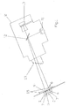
- both a UV light source 3 and a second light source 4 are installed in a housing 1 for light sources.
- the UV light source 3 can emit UV light in the range of 100-280 nm, in particular between 250 and 275 nm. It can be in the form of a UV-C luminaire, which is also called UV-C fluorescent lamp or UV-C fluorescent tube becomes. Likewise, one or more UV-C LEDs (LED line) can be used instead of a UV tube.
- the second light source 4 can emit light in the visible range (380-780 nm wavelength) and / or in the infrared range (780 nm-1 mm wavelength) and approximately - as in this example - as a fluorescent lamp (VIS light) with wavelengths in the visible range be executed.
- VIS light fluorescent lamp
- LED line one or more color or infrared LEDs (LED line) can be used.
- the disadvantage at least of LEDs in the UV-C range, are the currently high purchase costs and the higher diffuser costs compared to tube lights.
- the two light sources 3, 4 are separated by an opaque partition 5 from each other.
- Fig. 1 emits a UV-C lamp 3 UV-C radiation with a maximum intensity at a wavelength of 254 nm and is installed in the housing 1, that the UV light through a arranged behind the UV-C lamp 3 reflector 7 in Direction towards the detectors is passed.
- the UV light also passes through a filter 6, which absorbs a large part of the light emitted by the UV-C lamp 3 light in the visible range and thus conducts almost no visible light in the wavelength range of the fluorescent light to the detectors. If, for example, blue light were to pass from the UV-C lamp 3 to the detector for fluorescent light, this would be detected as fluorescent radiation, because it is likewise in the region of the blue light.
- the VIS light emitted by the second light source also passes through a filter 6 which absorbs emitted light in the UV and fluorescent region ( ⁇ 500 nm).
- the housing 1 consists of a quartz glass pane 9 at least in the region of the UV light transmission. Quartz glass has a high permeability to UV-C light. However, the quartz glass pane 9 can also cover the passage of light of the visible light.
- the quartz glass pane 9 also serves as a chute for the objects 15 to be examined (broken glass, contaminants). It has - in the mounted state of the device - an inclination of about 25 ° relative to the vertical. On her slide the objects 15 down and are illuminated by the two light sources 3, 4.
- the distance between the fluorescent light to be detected and the transmitted light to be detected should be as low as possible (ideally congruent), so that both detectors, those for fluorescence and that for transmission light, can image as closely as possible the moving object 15.
- the distance between the central axes of the light rays of the visible light and the UV light when they emerge from the housing 1 is about 50 mm in this example.
- Both the visible light transmitted through the objects of the VIS light 4 and the fluorescence radiation in the blue visible range which may be induced by the UV light pass through a protective glass 13 into the further housing 2, where on the one hand a detector 11 for detecting the fluorescent light is mounted On the other hand, where also a detector for detecting the transmission light of the second light source 4 is arranged.
- the protective glass 13 is made of normal glass and protects the interior of the housing 2 from dust and UV-C radiation.
- the detector 11 for detecting the fluorescent light is sensitive in a wavelength range of 400-1000 nm, the sensitivity can be further changed by filters, such as here on the relevant wavelength range of 420-500 nm. (If one UV light with a wavelength of about 270 nm, one would set the filter so that only fluorescent light in the wavelength range of 400-450 nm can be detected).
- the detector 11 will usually be designed as a camera. It can be designed for example as a so-called TDI camera 11.
- the second light source 4 may radiate as possible only light outside this frequency range. In practice, it is often the case that even light sources in the yellow or red area, which by definition "light in the visible range or emit IR light outside the wavelength range of the fluorescent light "still have a blue content in the light, and this may then have to be filtered out, as explained above in the filter 6 for the second light source 4.
- a detector 10 that is to say a camera, can deliver at least one image of glass pieces in shades of gray. From this, on the one hand, the position and shape of the object 15 can be determined, which is necessary in order to remove the object from the material flow, if appropriate by means of downstream discharge devices. On the other hand, this determines the light transmittance of the object (glass piece) 15 and recognizes it as transparent (it may then still contain lead or lead) or as little or not transparent (then it would be an impurity). Accordingly, the contaminant is then removed by the discharge from the flow of material. It is also possible by means of this detector to define the edges and interior regions of the glass pieces by image recognition and to use the intensity of the fluorescence radiation for evaluating the lead glass content only from these subareas of the sherd.
- Both fluorescent light and transmitted light impinge on a beam splitter 12 which as completely as possible reflects blue light, for example in the wavelength range of 400-500 nm, and transmits visible light> 500 nm (transmitted light) as completely as possible.
- the reflected light beam is passed into the TDI camera 11, the transmitted light beam into the RGB camera 10th
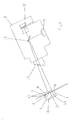
- a UV light source 3 and a second light source 14 are installed in a housing 1 for light sources again, but separated by an opaque partition 5 from each other.
- the UV light source 3 can emit UV light in the range of 100-280 nm, in particular between 250 and 275 nm. It is again designed here in the form of a UV-C lamp. Likewise, one or more UV-C LEDs could be used instead of a UV tube.
- the second light source 14 can emit light in the visible range (380-780 nm wavelength) and / or in the infrared range (780 nm-1 mm wavelength) and, as in this example, as one or more IR LEDs (LED line). be executed. Equally, however, a lamp with wavelengths in the visible range and / or in the infrared range or one or more daylight or color LEDs (LED line) could be used.
- the UV-C lamp 3 emits UV-C radiation with a wavelength of 254 nm and is incorporated in the housing 1, that the UV light directed by a reflector 7 arranged in the direction of the detectors away from the detectors and by two at right angles mutually arranged mirror filter 16 is deflected by 180 ° and thus directed towards the detectors.
- the mirror filters 16 are mirrors provided with a coating which occupies much of the absorbed by the UV-C lamp 3 light in the visible range and thus reflects almost no visible light in the wavelength range of the fluorescent light and leads to the detectors. If, for example, blue light were to pass from the UV-C lamp 3 to the detector for fluorescent light, this would be detected as fluorescent radiation, because it is likewise in the region of the blue light.
- visible light filters in the wavelength range of the fluorescent light could also be brought into the beam path of the UV light.
- Mirror filter 16 have the advantage that they can be produced inexpensively in large widths, about 1000mm, which corresponds to the width of conveyor belts or the slide for waste glass.
- classical filters have the disadvantage that they can often only be produced in small widths ( ⁇ 200 mm) and thus no one-piece filter can be produced for the device according to the invention, which can cover the entire width of the conveyor belt or the slide for waste glass.
- a mirror filter 16 in this example has a height (measured in the plane of the drawing) of about 5-10 cm, in particular 7 cm.
- the width (measured normal to drawing plane) is 50-150 cm, especially here 100 cm.
- a metal sheet having a thickness of 1-2 mm is used as a base material for the mirror filter 16.
- the coating consists of oxides and has a thickness of a few micrometers.
- the IR light of the IR LEDs 14 is passed through a diffusing screen 8 to make the light of the point IR LEDs 14 more homogeneous, and emerges from the housing 1 parallel to the UV light.
- a diffuser 8 can also others Means are used to distribute the light more evenly, such as a mirrored on its insides reflection channel, as in the AT 10184 U1 is shown.
- the housing 1 consists at least in the region of the UV light passage of a quartz glass plate 9 as in Fig. 1 ,
- the quartz glass pane 9 can also here cover the passage of light of the second light source, the IR LEDs 14, and serve as a chute for the objects to be examined.
- the distance between the fluorescent light to be detected and the transmitted light to be detected should also be as low as possible (ideally opaque), so that both detectors, those for fluorescence and that for transmission light, can image as closely as possible the moving object.
- the distance between the central axes of the light rays of the IR light and the UV light, if they emerge from the housing 1, in this example is also about 50mm.
- Both the IR light of the IR LEDs 14 transmitted by the objects 15 and the fluorescent radiation, which may be induced by the UV light, in the blue visible range pass through a protective glass 13 - as shown in FIG Fig. 1 in the further housing 2, where on the one hand a detector 11 is mounted for detecting the fluorescent light, the as under Fig. 1 is described and is also here in Fig. 2 is formed as a so-called TDI camera 11, and on the other hand, where a detector 10 for detecting the transmission light of the second light source 14, the IR LEDs 14, is arranged.
- the detector 10, usually a camera again, is therefore sensitive at least in that wavelength range in which the second light source 14 emits light, in this case in a range within the wavelength range of 780 nm -1 mm. It can also be here again an RGB camera, if necessary, with upstream filter can be used.
- the second light source may emit only light outside this frequency range as far as possible. It was therefore for this application example with respect to wavelength as far as possible from the fluorescent light remote light, namely IR light with a wavelength of 860 nm selected.
- the detector 10 For the detection of the transmission light is, as in Fig. 1 already explained, in principle sufficient if the detector 10, so as a camera, at least one image of objects 15 can deliver in shades of gray. From this, on the one hand, the position and shape of the object 15 can be determined, which is necessary in order to remove the object 15 from the material flow, if appropriate by means of downstream discharge devices. On the other hand, this determines the light transmittance of the object (glass piece) 15 and recognizes it as transparent (it may then still contain lead or lead) or as little or not transparent (then it would be an impurity). Accordingly, the contaminant is then removed by the discharge from the flow of material. It is also possible by means of this detector to define the edges and interior regions of the glass pieces by image recognition and to use the intensity of the fluorescence radiation for evaluating the lead glass content only from these subareas of the sherd.
Landscapes
- Health & Medical Sciences (AREA)
- Physics & Mathematics (AREA)
- Immunology (AREA)
- Analytical Chemistry (AREA)
- Biochemistry (AREA)
- General Health & Medical Sciences (AREA)
- General Physics & Mathematics (AREA)
- Life Sciences & Earth Sciences (AREA)
- Pathology (AREA)
- Chemical & Material Sciences (AREA)
- Engineering & Computer Science (AREA)
- Microelectronics & Electronic Packaging (AREA)
- Nuclear Medicine, Radiotherapy & Molecular Imaging (AREA)
- Manufacturing & Machinery (AREA)
- Optics & Photonics (AREA)
- Investigating Materials By The Use Of Optical Means Adapted For Particular Applications (AREA)
- Investigating, Analyzing Materials By Fluorescence Or Luminescence (AREA)
- Investigating Or Analysing Materials By Optical Means (AREA)
- Sorting Of Articles (AREA)
Priority Applications (1)
| Application Number | Priority Date | Filing Date | Title |
|---|---|---|---|
| PL14176570T PL2808672T3 (pl) | 2009-08-19 | 2010-02-26 | Obudowa dla źródła światła UV |
Applications Claiming Priority (3)
| Application Number | Priority Date | Filing Date | Title |
|---|---|---|---|
| AT0052009U AT11769U1 (de) | 2009-08-19 | 2009-08-19 | Verfahren und vorrichtung zum detektieren von bleihältigen glasstücken |
| PCT/EP2010/052457 WO2011020628A1 (de) | 2009-08-19 | 2010-02-26 | Verfahren und vorrichtung zum detektieren von bleihältigen glasstücken |
| EP10709457.5A EP2467702B1 (de) | 2009-08-19 | 2010-02-26 | Verfahren und vorrichtung zum detektieren von bleihältigen glasstücken |
Related Parent Applications (2)
| Application Number | Title | Priority Date | Filing Date |
|---|---|---|---|
| EP10709457.5A Division-Into EP2467702B1 (de) | 2009-08-19 | 2010-02-26 | Verfahren und vorrichtung zum detektieren von bleihältigen glasstücken |
| EP10709457.5A Division EP2467702B1 (de) | 2009-08-19 | 2010-02-26 | Verfahren und vorrichtung zum detektieren von bleihältigen glasstücken |
Publications (2)
| Publication Number | Publication Date |
|---|---|
| EP2808672A1 EP2808672A1 (de) | 2014-12-03 |
| EP2808672B1 true EP2808672B1 (de) | 2018-10-31 |
Family
ID=43568420
Family Applications (2)
| Application Number | Title | Priority Date | Filing Date |
|---|---|---|---|
| EP14176570.1A Active EP2808672B1 (de) | 2009-08-19 | 2010-02-26 | Gehäuse für eine UV-Lichtquelle |
| EP10709457.5A Active EP2467702B1 (de) | 2009-08-19 | 2010-02-26 | Verfahren und vorrichtung zum detektieren von bleihältigen glasstücken |
Family Applications After (1)
| Application Number | Title | Priority Date | Filing Date |
|---|---|---|---|
| EP10709457.5A Active EP2467702B1 (de) | 2009-08-19 | 2010-02-26 | Verfahren und vorrichtung zum detektieren von bleihältigen glasstücken |
Country Status (9)
| Country | Link |
|---|---|
| US (1) | US8803020B2 (pl) |
| EP (2) | EP2808672B1 (pl) |
| AT (1) | AT11769U1 (pl) |
| AU (1) | AU2010285188C1 (pl) |
| DK (2) | DK2467702T3 (pl) |
| ES (2) | ES2526557T3 (pl) |
| PL (2) | PL2467702T3 (pl) |
| PT (2) | PT2467702E (pl) |
| WO (1) | WO2011020628A1 (pl) |
Families Citing this family (14)
| Publication number | Priority date | Publication date | Assignee | Title |
|---|---|---|---|---|
| CN103934222A (zh) * | 2014-04-28 | 2014-07-23 | 安徽捷迅光电技术有限公司 | 一种多角度色选的色选机色选光源结构 |
| AT15295U1 (de) | 2015-03-09 | 2017-05-15 | Binder + Co Ag | Aussortieren von mineralienhaltigen Objekten oder Kunststoff-Objekten |
| AT15419U1 (de) | 2015-05-19 | 2017-08-15 | Binder + Co Ag | Verfahren und vorrichtung zur einstellung der in einen optischen detektor gelangenden strahlungsleistung |
| AT15723U1 (de) * | 2016-08-30 | 2018-04-15 | Binder Co Ag | Vorrichtung zum Detektieren von Objekten in einem Materialstrom |
| JP6892249B2 (ja) * | 2016-11-24 | 2021-06-23 | 東洋ガラス株式会社 | カレット分別装置およびカレット分別方法 |
| CN109732765B (zh) * | 2018-12-27 | 2021-05-18 | 佛山欧神诺陶瓷有限公司 | 一种用于瓷砖识别、记录、跟踪和分选的方法 |
| CN111451176A (zh) * | 2019-01-21 | 2020-07-28 | 合肥泰禾光电科技股份有限公司 | 一种用于物料分选设备的探测装置、物料分选设备及方法 |
| FR3095273B1 (fr) * | 2019-04-19 | 2021-05-07 | Saint Gobain Isover | Système de détection automatisé de matériaux de type vitrocéramique |
| DE102019114033A1 (de) * | 2019-05-26 | 2020-11-26 | Dieffenbacher GmbH Maschinen- und Anlagenbau | Überwachungsvorrichtung zur Erfassung wenigstens einer Stoffkomponente in zerkleinerten Werkstoffen, Förderanlage für zerkleinerte Werkstoffe und Verfahren zur Überwachung von zerkleinerten Werkstoffen |
| IT202000007345A1 (it) * | 2020-04-07 | 2021-10-07 | Stazione Sperimentale Del Vetro Soc Consortile Per Azioni In Sigla Stazione Sperimentale Del Vetro S | Attrezzatura per la rilevazione di elementi inquinanti in rottami di vetro |
| US12105053B2 (en) | 2021-04-21 | 2024-10-01 | Hong Kong Applied Science and Technology Research Institute Company Limited | Apparatus and method for classifying glass object using acoustic analysis |
| CN113976480B (zh) * | 2021-12-27 | 2022-04-01 | 北京霍里思特科技有限公司 | 一种双光谱融合智能选矿系统 |
| EP4520448A1 (de) * | 2023-09-07 | 2025-03-12 | Binder + Co AG | Aussortieren von altglasscherben mit einem höheren gehalt an eisenoxid |
| CN119456426B (zh) * | 2024-11-11 | 2025-11-18 | 佛山华兴玻璃有限公司 | 检测缺陷显示方法、系统、装置及介质 |
Family Cites Families (18)
| Publication number | Priority date | Publication date | Assignee | Title |
|---|---|---|---|---|
| DE3504793A1 (de) * | 1985-02-13 | 1986-08-14 | W.C. Heraeus Gmbh, 6450 Hanau | Beleuchtungsanordnung, insbesondere fuer licht- und wetterechtheitspruefgeraete |
| DE3618173A1 (de) * | 1986-05-30 | 1987-12-03 | Mab Marlis Kellermann | Glas-sortieranlage |
| FR2604377B1 (fr) | 1986-09-29 | 1990-04-20 | Boussois Souchon Neuvesel Sa | Dispositif de tri optique du groisil |
| US5314071A (en) * | 1992-12-10 | 1994-05-24 | Fmc Corporation | Glass sorter |
| DE4339822C1 (de) | 1993-11-23 | 1995-05-24 | Noell Gmbh | Verfahren und Vorrichtung zur Sortierung von anorganischen nichtmetallischen Werkstoffen |
| US5663997A (en) * | 1995-01-27 | 1997-09-02 | Asoma Instruments, Inc. | Glass composition determination method and apparatus |
| US7355140B1 (en) * | 2002-08-12 | 2008-04-08 | Ecullet | Method of and apparatus for multi-stage sorting of glass cullets |
| WO2004063729A1 (de) | 2003-01-10 | 2004-07-29 | Schott Ag | Verfahren und vorrichtung zur selektion von recyclingglas |
| US7264124B2 (en) * | 2003-11-17 | 2007-09-04 | Casella Waste Systems, Inc. | Systems and methods for sorting recyclables at a material recovery facility |
| US7918343B2 (en) * | 2003-11-17 | 2011-04-05 | Casella Waste Systems, Inc. | Systems and methods for glass recycling at a beneficiator |
| US7757863B2 (en) * | 2003-11-17 | 2010-07-20 | Casella Waste Systems, Inc. | Systems and methods for glass recycling at a beneficiator and/or a material recovery facility |
| EP1764611B1 (en) * | 2004-05-27 | 2011-09-14 | Panasonic Corporation | Method of Glass Recovery |
| US7216997B2 (en) * | 2004-10-26 | 2007-05-15 | Federal-Mogul World Wide, Inc. | Phosphor reactive instrument panel and gauges |
| DE202004017833U1 (de) * | 2004-11-17 | 2005-01-05 | Atlas Material Testing Technology Gmbh | Strahlungsquellen-Aufnahmeeinheit für ein Bewitterungsgerät |
| AT8647U1 (de) | 2005-08-08 | 2006-10-15 | Binder Co Ag | Verfahren zur detektion und sortierung von glas |
| US7659486B2 (en) * | 2005-10-20 | 2010-02-09 | Valerio Thomas A | Method and apparatus for sorting contaminated glass |
| WO2007143047A1 (en) | 2006-06-01 | 2007-12-13 | Ecolab Inc. | Uv fluorometric sensor and method for using the same |
| AT10184U1 (de) | 2008-01-24 | 2008-10-15 | Binder Co Ag | Vorrichtung zum erfassen und erkennen von objekten |
-
2009
- 2009-08-19 AT AT0052009U patent/AT11769U1/de not_active IP Right Cessation
-
2010
- 2010-02-26 US US13/390,970 patent/US8803020B2/en active Active
- 2010-02-26 AU AU2010285188A patent/AU2010285188C1/en active Active
- 2010-02-26 PL PL10709457T patent/PL2467702T3/pl unknown
- 2010-02-26 EP EP14176570.1A patent/EP2808672B1/de active Active
- 2010-02-26 ES ES10709457.5T patent/ES2526557T3/es active Active
- 2010-02-26 DK DK10709457.5T patent/DK2467702T3/en active
- 2010-02-26 DK DK14176570.1T patent/DK2808672T3/en active
- 2010-02-26 PT PT107094575T patent/PT2467702E/pt unknown
- 2010-02-26 EP EP10709457.5A patent/EP2467702B1/de active Active
- 2010-02-26 PL PL14176570T patent/PL2808672T3/pl unknown
- 2010-02-26 ES ES14176570T patent/ES2705857T3/es active Active
- 2010-02-26 PT PT14176570T patent/PT2808672T/pt unknown
- 2010-02-26 WO PCT/EP2010/052457 patent/WO2011020628A1/de not_active Ceased
Non-Patent Citations (1)
| Title |
|---|
| None * |
Also Published As
| Publication number | Publication date |
|---|---|
| PL2808672T3 (pl) | 2019-04-30 |
| WO2011020628A1 (de) | 2011-02-24 |
| EP2467702B1 (de) | 2014-09-17 |
| DK2467702T3 (en) | 2014-12-15 |
| AT11769U1 (de) | 2011-04-15 |
| PL2467702T3 (pl) | 2015-03-31 |
| AU2010285188C1 (en) | 2014-11-20 |
| US20120145607A1 (en) | 2012-06-14 |
| DK2808672T3 (en) | 2019-01-28 |
| US8803020B2 (en) | 2014-08-12 |
| PT2808672T (pt) | 2019-01-10 |
| AU2010285188B2 (en) | 2014-08-07 |
| ES2705857T3 (es) | 2019-03-26 |
| ES2526557T3 (es) | 2015-01-13 |
| EP2808672A1 (de) | 2014-12-03 |
| AU2010285188A1 (en) | 2012-02-23 |
| EP2467702A1 (de) | 2012-06-27 |
| PT2467702E (pt) | 2015-01-02 |
Similar Documents
| Publication | Publication Date | Title |
|---|---|---|
| EP2808672B1 (de) | Gehäuse für eine UV-Lichtquelle | |
| EP3107664B1 (de) | Aussortieren von mineralienhaltigen objekten oder kunststoff-objekten | |
| DE3516752C2 (pl) | ||
| EP2089168B1 (de) | Vorrichtung und verfarhen zur optischen sortierung von schüttgut | |
| EP3757553B1 (de) | Vorrichtung zur optischen inspektion von leeren und mit flüssigkeit gefüllten behältern | |
| EP1752228A1 (de) | Verfahren und Vorrichtung zur Detektion und Sortierung von Glas | |
| DE102010012570A1 (de) | Vorrichtung und Verfahren zum Untersuchen von befüllten Behältnissen auf Fremdkörper | |
| WO2018041902A1 (de) | Vorrichtung zum detektieren von objekten in einem materialstrom | |
| EP3980760A1 (de) | Verfahren und vorrichtung zur optischen inspektion von behältern | |
| EP1581802B1 (de) | Verfahren und vorrichtung zur selektion von recyclingglas | |
| AT15588U1 (de) | Vorrichtung und Verfahren zur Detektion von Objekten, insbesondere von Objekten in einem Materialstrom | |
| DE102014005932A1 (de) | Verfahren und Vorrichtung zur Selektion und Detektion von Nickelsulfid-Einschlüssen in Glas | |
| DE707745C (de) | Photometrische Einrichtung zur lichtelektrischen Untersuchung von Loechern | |
| EP3095531A1 (de) | Verfahren und vorrichtung zur einstellung der in einen optischen detektor gelangenden strahlungsleistung | |
| DE102018222185B4 (de) | Verfahren zum Recycling von LED-Komponenten aus Altlampenmischungen | |
| DE102005003406B4 (de) | Verfahren und Vorrichtung zum Recycling von Glaskeramiken | |
| EP2083261B1 (de) | Vorrichtung zum Erfassen und Erkennen von Objekten | |
| DE202004009165U1 (de) | Vorrichtung zur Sortierung von lichtbrechenden Partikeln | |
| CH617769A5 (en) | Method and device for identifying bodies containing or carrying a luminous material | |
| DE4421919A1 (de) | Gerät zur Überprüfung der Konstanz der Farbtemperatur einer Lichtquelle |
Legal Events
| Date | Code | Title | Description |
|---|---|---|---|
| PUAI | Public reference made under article 153(3) epc to a published international application that has entered the european phase |
Free format text: ORIGINAL CODE: 0009012 |
|
| 17P | Request for examination filed |
Effective date: 20140710 |
|
| AC | Divisional application: reference to earlier application |
Ref document number: 2467702 Country of ref document: EP Kind code of ref document: P |
|
| AK | Designated contracting states |
Kind code of ref document: A1 Designated state(s): AT BE BG CH CY CZ DE DK EE ES FI FR GB GR HR HU IE IS IT LI LT LU LV MC MK MT NL NO PL PT RO SE SI SK SM TR |
|
| R17P | Request for examination filed (corrected) |
Effective date: 20150603 |
|
| RBV | Designated contracting states (corrected) |
Designated state(s): AT BE BG CH CY CZ DE DK EE ES FI FR GB GR HR HU IE IS IT LI LT LU LV MC MK MT NL NO PL PT RO SE SI SK SM TR |
|
| STAA | Information on the status of an ep patent application or granted ep patent |
Free format text: STATUS: EXAMINATION IS IN PROGRESS |
|
| 17Q | First examination report despatched |
Effective date: 20171011 |
|
| GRAP | Despatch of communication of intention to grant a patent |
Free format text: ORIGINAL CODE: EPIDOSNIGR1 |
|
| STAA | Information on the status of an ep patent application or granted ep patent |
Free format text: STATUS: GRANT OF PATENT IS INTENDED |
|
| INTG | Intention to grant announced |
Effective date: 20180315 |
|
| GRAS | Grant fee paid |
Free format text: ORIGINAL CODE: EPIDOSNIGR3 |
|
| GRAJ | Information related to disapproval of communication of intention to grant by the applicant or resumption of examination proceedings by the epo deleted |
Free format text: ORIGINAL CODE: EPIDOSDIGR1 |
|
| GRAL | Information related to payment of fee for publishing/printing deleted |
Free format text: ORIGINAL CODE: EPIDOSDIGR3 |
|
| STAA | Information on the status of an ep patent application or granted ep patent |
Free format text: STATUS: EXAMINATION IS IN PROGRESS |
|
| INTC | Intention to grant announced (deleted) | ||
| GRAP | Despatch of communication of intention to grant a patent |
Free format text: ORIGINAL CODE: EPIDOSNIGR1 |
|
| STAA | Information on the status of an ep patent application or granted ep patent |
Free format text: STATUS: GRANT OF PATENT IS INTENDED |
|
| INTG | Intention to grant announced |
Effective date: 20180829 |
|
| GRAA | (expected) grant |
Free format text: ORIGINAL CODE: 0009210 |
|
| STAA | Information on the status of an ep patent application or granted ep patent |
Free format text: STATUS: THE PATENT HAS BEEN GRANTED |
|
| AC | Divisional application: reference to earlier application |
Ref document number: 2467702 Country of ref document: EP Kind code of ref document: P |
|
| AK | Designated contracting states |
Kind code of ref document: B1 Designated state(s): AT BE BG CH CY CZ DE DK EE ES FI FR GB GR HR HU IE IS IT LI LT LU LV MC MK MT NL NO PL PT RO SE SI SK SM TR |
|
| REG | Reference to a national code |
Ref country code: CH Ref legal event code: EP Ref country code: GB Ref legal event code: FG4D Free format text: NOT ENGLISH |
|
| REG | Reference to a national code |
Ref country code: AT Ref legal event code: REF Ref document number: 1059978 Country of ref document: AT Kind code of ref document: T Effective date: 20181115 |
|
| REG | Reference to a national code |
Ref country code: DE Ref legal event code: R096 Ref document number: 502010015526 Country of ref document: DE |
|
| REG | Reference to a national code |
Ref country code: IE Ref legal event code: FG4D Free format text: LANGUAGE OF EP DOCUMENT: GERMAN |
|
| REG | Reference to a national code |
Ref country code: CH Ref legal event code: NV Representative=s name: PATENTANWAELTE SCHAAD, BALASS, MENZL AND PARTN, CH |
|
| REG | Reference to a national code |
Ref country code: PT Ref legal event code: SC4A Ref document number: 2808672 Country of ref document: PT Date of ref document: 20190110 Kind code of ref document: T Free format text: AVAILABILITY OF NATIONAL TRANSLATION Effective date: 20181221 |
|
| REG | Reference to a national code |
Ref country code: NL Ref legal event code: FP |
|
| REG | Reference to a national code |
Ref country code: DK Ref legal event code: T3 Effective date: 20190123 |
|
| REG | Reference to a national code |
Ref country code: SE Ref legal event code: TRGR |
|
| REG | Reference to a national code |
Ref country code: LT Ref legal event code: MG4D |
|
| REG | Reference to a national code |
Ref country code: ES Ref legal event code: FG2A Ref document number: 2705857 Country of ref document: ES Kind code of ref document: T3 Effective date: 20190326 |
|
| PG25 | Lapsed in a contracting state [announced via postgrant information from national office to epo] |
Ref country code: IS Free format text: LAPSE BECAUSE OF FAILURE TO SUBMIT A TRANSLATION OF THE DESCRIPTION OR TO PAY THE FEE WITHIN THE PRESCRIBED TIME-LIMIT Effective date: 20190228 Ref country code: LV Free format text: LAPSE BECAUSE OF FAILURE TO SUBMIT A TRANSLATION OF THE DESCRIPTION OR TO PAY THE FEE WITHIN THE PRESCRIBED TIME-LIMIT Effective date: 20181031 Ref country code: NO Free format text: LAPSE BECAUSE OF FAILURE TO SUBMIT A TRANSLATION OF THE DESCRIPTION OR TO PAY THE FEE WITHIN THE PRESCRIBED TIME-LIMIT Effective date: 20190131 Ref country code: FI Free format text: LAPSE BECAUSE OF FAILURE TO SUBMIT A TRANSLATION OF THE DESCRIPTION OR TO PAY THE FEE WITHIN THE PRESCRIBED TIME-LIMIT Effective date: 20181031 Ref country code: LT Free format text: LAPSE BECAUSE OF FAILURE TO SUBMIT A TRANSLATION OF THE DESCRIPTION OR TO PAY THE FEE WITHIN THE PRESCRIBED TIME-LIMIT Effective date: 20181031 Ref country code: BG Free format text: LAPSE BECAUSE OF FAILURE TO SUBMIT A TRANSLATION OF THE DESCRIPTION OR TO PAY THE FEE WITHIN THE PRESCRIBED TIME-LIMIT Effective date: 20190131 Ref country code: HR Free format text: LAPSE BECAUSE OF FAILURE TO SUBMIT A TRANSLATION OF THE DESCRIPTION OR TO PAY THE FEE WITHIN THE PRESCRIBED TIME-LIMIT Effective date: 20181031 |
|
| PG25 | Lapsed in a contracting state [announced via postgrant information from national office to epo] |
Ref country code: GR Free format text: LAPSE BECAUSE OF FAILURE TO SUBMIT A TRANSLATION OF THE DESCRIPTION OR TO PAY THE FEE WITHIN THE PRESCRIBED TIME-LIMIT Effective date: 20190201 |
|
| PG25 | Lapsed in a contracting state [announced via postgrant information from national office to epo] |
Ref country code: CZ Free format text: LAPSE BECAUSE OF FAILURE TO SUBMIT A TRANSLATION OF THE DESCRIPTION OR TO PAY THE FEE WITHIN THE PRESCRIBED TIME-LIMIT Effective date: 20181031 |
|
| REG | Reference to a national code |
Ref country code: DE Ref legal event code: R097 Ref document number: 502010015526 Country of ref document: DE |
|
| PG25 | Lapsed in a contracting state [announced via postgrant information from national office to epo] |
Ref country code: RO Free format text: LAPSE BECAUSE OF FAILURE TO SUBMIT A TRANSLATION OF THE DESCRIPTION OR TO PAY THE FEE WITHIN THE PRESCRIBED TIME-LIMIT Effective date: 20181031 Ref country code: SM Free format text: LAPSE BECAUSE OF FAILURE TO SUBMIT A TRANSLATION OF THE DESCRIPTION OR TO PAY THE FEE WITHIN THE PRESCRIBED TIME-LIMIT Effective date: 20181031 Ref country code: EE Free format text: LAPSE BECAUSE OF FAILURE TO SUBMIT A TRANSLATION OF THE DESCRIPTION OR TO PAY THE FEE WITHIN THE PRESCRIBED TIME-LIMIT Effective date: 20181031 Ref country code: SK Free format text: LAPSE BECAUSE OF FAILURE TO SUBMIT A TRANSLATION OF THE DESCRIPTION OR TO PAY THE FEE WITHIN THE PRESCRIBED TIME-LIMIT Effective date: 20181031 |
|
| PLBE | No opposition filed within time limit |
Free format text: ORIGINAL CODE: 0009261 |
|
| STAA | Information on the status of an ep patent application or granted ep patent |
Free format text: STATUS: NO OPPOSITION FILED WITHIN TIME LIMIT |
|
| 26N | No opposition filed |
Effective date: 20190801 |
|
| PG25 | Lapsed in a contracting state [announced via postgrant information from national office to epo] |
Ref country code: MC Free format text: LAPSE BECAUSE OF FAILURE TO SUBMIT A TRANSLATION OF THE DESCRIPTION OR TO PAY THE FEE WITHIN THE PRESCRIBED TIME-LIMIT Effective date: 20181031 Ref country code: LU Free format text: LAPSE BECAUSE OF NON-PAYMENT OF DUE FEES Effective date: 20190226 Ref country code: SI Free format text: LAPSE BECAUSE OF FAILURE TO SUBMIT A TRANSLATION OF THE DESCRIPTION OR TO PAY THE FEE WITHIN THE PRESCRIBED TIME-LIMIT Effective date: 20181031 |
|
| REG | Reference to a national code |
Ref country code: IE Ref legal event code: MM4A |
|
| PG25 | Lapsed in a contracting state [announced via postgrant information from national office to epo] |
Ref country code: IE Free format text: LAPSE BECAUSE OF NON-PAYMENT OF DUE FEES Effective date: 20190226 |
|
| PGFP | Annual fee paid to national office [announced via postgrant information from national office to epo] |
Ref country code: PL Payment date: 20200116 Year of fee payment: 11 |
|
| PGFP | Annual fee paid to national office [announced via postgrant information from national office to epo] |
Ref country code: CH Payment date: 20200204 Year of fee payment: 11 |
|
| PG25 | Lapsed in a contracting state [announced via postgrant information from national office to epo] |
Ref country code: MT Free format text: LAPSE BECAUSE OF FAILURE TO SUBMIT A TRANSLATION OF THE DESCRIPTION OR TO PAY THE FEE WITHIN THE PRESCRIBED TIME-LIMIT Effective date: 20181031 |
|
| PGFP | Annual fee paid to national office [announced via postgrant information from national office to epo] |
Ref country code: TR Payment date: 20200129 Year of fee payment: 11 |
|
| PG25 | Lapsed in a contracting state [announced via postgrant information from national office to epo] |
Ref country code: CY Free format text: LAPSE BECAUSE OF FAILURE TO SUBMIT A TRANSLATION OF THE DESCRIPTION OR TO PAY THE FEE WITHIN THE PRESCRIBED TIME-LIMIT Effective date: 20181031 |
|
| PG25 | Lapsed in a contracting state [announced via postgrant information from national office to epo] |
Ref country code: HU Free format text: LAPSE BECAUSE OF FAILURE TO SUBMIT A TRANSLATION OF THE DESCRIPTION OR TO PAY THE FEE WITHIN THE PRESCRIBED TIME-LIMIT; INVALID AB INITIO Effective date: 20100226 |
|
| PG25 | Lapsed in a contracting state [announced via postgrant information from national office to epo] |
Ref country code: LI Free format text: LAPSE BECAUSE OF NON-PAYMENT OF DUE FEES Effective date: 20210228 Ref country code: CH Free format text: LAPSE BECAUSE OF NON-PAYMENT OF DUE FEES Effective date: 20210228 |
|
| PG25 | Lapsed in a contracting state [announced via postgrant information from national office to epo] |
Ref country code: MK Free format text: LAPSE BECAUSE OF FAILURE TO SUBMIT A TRANSLATION OF THE DESCRIPTION OR TO PAY THE FEE WITHIN THE PRESCRIBED TIME-LIMIT Effective date: 20181031 |
|
| PG25 | Lapsed in a contracting state [announced via postgrant information from national office to epo] |
Ref country code: PL Free format text: LAPSE BECAUSE OF NON-PAYMENT OF DUE FEES Effective date: 20210226 |
|
| P01 | Opt-out of the competence of the unified patent court (upc) registered |
Effective date: 20230517 |
|
| PGFP | Annual fee paid to national office [announced via postgrant information from national office to epo] |
Ref country code: NL Payment date: 20250221 Year of fee payment: 16 |
|
| PGFP | Annual fee paid to national office [announced via postgrant information from national office to epo] |
Ref country code: DE Payment date: 20250225 Year of fee payment: 16 Ref country code: PT Payment date: 20250122 Year of fee payment: 16 |
|
| PGFP | Annual fee paid to national office [announced via postgrant information from national office to epo] |
Ref country code: DK Payment date: 20250224 Year of fee payment: 16 |
|
| PGFP | Annual fee paid to national office [announced via postgrant information from national office to epo] |
Ref country code: ES Payment date: 20250303 Year of fee payment: 16 |
|
| PGFP | Annual fee paid to national office [announced via postgrant information from national office to epo] |
Ref country code: SE Payment date: 20250224 Year of fee payment: 16 |
|
| PGFP | Annual fee paid to national office [announced via postgrant information from national office to epo] |
Ref country code: AT Payment date: 20250221 Year of fee payment: 16 Ref country code: BE Payment date: 20250129 Year of fee payment: 16 |
|
| PGFP | Annual fee paid to national office [announced via postgrant information from national office to epo] |
Ref country code: FR Payment date: 20250127 Year of fee payment: 16 |
|
| PGFP | Annual fee paid to national office [announced via postgrant information from national office to epo] |
Ref country code: IT Payment date: 20250205 Year of fee payment: 16 Ref country code: GB Payment date: 20250221 Year of fee payment: 16 |