EP2806655B1 - Audio interface adapter device and audio signal receiving apparatus - Google Patents
Audio interface adapter device and audio signal receiving apparatus Download PDFInfo
- Publication number
- EP2806655B1 EP2806655B1 EP12865732.7A EP12865732A EP2806655B1 EP 2806655 B1 EP2806655 B1 EP 2806655B1 EP 12865732 A EP12865732 A EP 12865732A EP 2806655 B1 EP2806655 B1 EP 2806655B1
- Authority
- EP
- European Patent Office
- Prior art keywords
- pin
- conductive element
- audio
- unidirectional conductive
- mos transistor
- Prior art date
- Legal status (The legal status is an assumption and is not a legal conclusion. Google has not performed a legal analysis and makes no representation as to the accuracy of the status listed.)
- Not-in-force
Links
Images


Classifications
-
- H—ELECTRICITY
- H04—ELECTRIC COMMUNICATION TECHNIQUE
- H04R—LOUDSPEAKERS, MICROPHONES, GRAMOPHONE PICK-UPS OR LIKE ACOUSTIC ELECTROMECHANICAL TRANSDUCERS; DEAF-AID SETS; PUBLIC ADDRESS SYSTEMS
- H04R3/00—Circuits for transducers, loudspeakers or microphones
-
- H—ELECTRICITY
- H04—ELECTRIC COMMUNICATION TECHNIQUE
- H04R—LOUDSPEAKERS, MICROPHONES, GRAMOPHONE PICK-UPS OR LIKE ACOUSTIC ELECTROMECHANICAL TRANSDUCERS; DEAF-AID SETS; PUBLIC ADDRESS SYSTEMS
- H04R29/00—Monitoring arrangements; Testing arrangements
-
- H—ELECTRICITY
- H04—ELECTRIC COMMUNICATION TECHNIQUE
- H04R—LOUDSPEAKERS, MICROPHONES, GRAMOPHONE PICK-UPS OR LIKE ACOUSTIC ELECTROMECHANICAL TRANSDUCERS; DEAF-AID SETS; PUBLIC ADDRESS SYSTEMS
- H04R29/00—Monitoring arrangements; Testing arrangements
- H04R29/001—Monitoring arrangements; Testing arrangements for loudspeakers
- H04R29/002—Loudspeaker arrays
-
- H—ELECTRICITY
- H04—ELECTRIC COMMUNICATION TECHNIQUE
- H04R—LOUDSPEAKERS, MICROPHONES, GRAMOPHONE PICK-UPS OR LIKE ACOUSTIC ELECTROMECHANICAL TRANSDUCERS; DEAF-AID SETS; PUBLIC ADDRESS SYSTEMS
- H04R29/00—Monitoring arrangements; Testing arrangements
- H04R29/004—Monitoring arrangements; Testing arrangements for microphones
-
- G—PHYSICS
- G06—COMPUTING; CALCULATING OR COUNTING
- G06F—ELECTRIC DIGITAL DATA PROCESSING
- G06F3/00—Input arrangements for transferring data to be processed into a form capable of being handled by the computer; Output arrangements for transferring data from processing unit to output unit, e.g. interface arrangements
- G06F3/16—Sound input; Sound output
- G06F3/162—Interface to dedicated audio devices, e.g. audio drivers, interface to CODECs
-
- H—ELECTRICITY
- H04—ELECTRIC COMMUNICATION TECHNIQUE
- H04R—LOUDSPEAKERS, MICROPHONES, GRAMOPHONE PICK-UPS OR LIKE ACOUSTIC ELECTROMECHANICAL TRANSDUCERS; DEAF-AID SETS; PUBLIC ADDRESS SYSTEMS
- H04R2420/00—Details of connection covered by H04R, not provided for in its groups
-
- H—ELECTRICITY
- H04—ELECTRIC COMMUNICATION TECHNIQUE
- H04R—LOUDSPEAKERS, MICROPHONES, GRAMOPHONE PICK-UPS OR LIKE ACOUSTIC ELECTROMECHANICAL TRANSDUCERS; DEAF-AID SETS; PUBLIC ADDRESS SYSTEMS
- H04R2420/00—Details of connection covered by H04R, not provided for in its groups
- H04R2420/05—Detection of connection of loudspeakers or headphones to amplifiers
Definitions
- the present disclosure generally relates to an electronic technique field, and more particularly relates to an audio interface adapter device and an audio signal receiving apparatus.
- An audio interface (such as a headphone socket) of an existing audio signal sending apparatus (such as a mobile communication terminal) and an audio interface of an audio signal receiving apparatus (such as a headphone) generally use a four-section interface, in which a pin 1 and a pin 2 are audio pins, i.e., a left-channel pin and a right-channel pin respectively.
- a pin 3 and a pin 4 of different types of audio interfaces play different roles, that is, there are two types of audio interfaces: the pin 3 is a MIC pin (a microphone pin) and the pin 4 is a GND pin (a ground pin); the pin 3 is a GND pin and the pin 4 is a MIC pin.
- the audio signal sending apparatus can neither communicate with the audio signal receiving apparatus via the MIC pin of the audio interface, nor transmit an audio signal to the audio signal receiving apparatus via the audio pins (i.e., the left-channel pin and the right-channel pin) of the audio interface normally.
- US 2009/130910 A1 discloses an apparatus including a first connector and a switching system.
- the first connector is configured to receive a second connector having a first contact area and a second different contact area.
- the switching system is connected to the first connector and configured to alternatively connect a ground of the apparatus to the first or the second contact area.
- US 2005/090141 A1 discloses a plug detection circuit.
- the detected circuit is disposed in an electronics device with an earphone jack, accepting plugs with a plurality of conductive rings.
- the detection circuit has a plurality of pins, wherein a first pin detects, and outputs a first logic potential, and a second pin detects the potentials at the conductive rings and outputs a second logic potential.
- the detection circuit determines the type of earphone connected to the earphone jack.
- US 6 856 046 B1 discloses a plug-in device discrimination circuit connected to the contacts of a jack.
- the technical problem to be solved by the present disclosure is to overcome the defects of the prior art, and to provide an audio interface adapter device (adapter circuit) and an audio signal receiving apparatus (such as a headphone, a headset, a loudspeaker, an audio signal adapter apparatus, and other audio signal receiving apparatuses receiving an audio signal via an audio pin and processing the audio signal) provided with the audio interface adapter device.
- the audio interface adapter device can receive the audio signal normally via the audio pin (a left-channel pin, and/or a right-channel pin) of an audio interface when being connected with an audio signal sending apparatus provided with any type of audio interface.
- the present disclosure provides an audio interface adapter device.
- the device comprises an audio interface.
- the audio interface comprises a pin 1, a pin 2, a pin 3 and a pin 4.
- An audio pin of the audio interface is connected with the pin 3 via a first unidirectional conductive element, and connected with the pin 4 via a second unidirectional conductive element.
- the audio pin comprises the pin 1 and/or the pin 2.
- One of the pin 3 and the pin 4 is used as a microphone pin, and the other one of the pin 3 and the pin 4 is used as a ground pin.
- a conductive direction of the first unidirectional conductive element is from the audio pin to the pin 3, and a conductive direction of the second unidirectional conductive element is from the audio pin to the pin 4.
- the pin 1 is connected with the pin 3 via a first signal processing unit and via the first unidirectional conductive element in sequence, and connected with the pin 4 via the first signal processing unit and via the second unidirectional conductive element in sequence; and/or the pin 2 is connected with the pin 3 via a second signal processing unit and via the first unidirectional conductive element in sequence, and connected with the pin 4 via the second signal processing unit and via the second unidirectional conductive element in sequence.
- the device further comprises a first bidirectional conductive element.
- One terminal of the first bidirectional conductive element is connected with the pin 3 and the first unidirectional conductive element respectively, and the other terminal of the first bidirectional conductive element is connected with the pin 4 and the second unidirectional conductive element respectively.
- the first bidirectional conductive element is a resistor.
- the first unidirectional conductive element is one of a diode, a triode and a MOS transistor
- the second unidirectional conductive element is one of a diode, a triode and a MOS transistor.
- the first unidirectional conductive element is a diode D1, an anode of the diode D1 is connected with the audio pin, and a cathode of the diode D1 is connected with the pin 3; and/or the second unidirectional conductive element is a diode D2, an anode of the diode D2 is connected with the audio pin, and a cathode of the diode D2 is connected with the pin 4.
- the first unidirectional conductive element is a PNP triode T1, an emitter of the PNP triode T1 is connected with the audio pin, and a base of the PNP triode T1 is connected with the pin 3; and/or the second unidirectional conductive element is a PNP triode T2, an emitter of the PNP triode T2 is connected with the audio pin, and a base of the PNP triode T2 is connected with the pin 4.
- the first unidirectional conductive element is an NPN triode T1, a base of the NPN triode T1 is connected with the audio pin, and an emitter of the NPN triode T1 is connected with the pin 3; and/or the second unidirectional conductive element is an NPN triode T2, a base of the NPN triode T2 is connected with the audio pin, and an emitter of the NPN triode T2 is connected with the pin 4.
- the first unidirectional conductive element is an N-channel junction MOS transistor F1, a source of the N-channel junction MOS transistor F1 is connected with the audio pin, and a gate of the N-channel junction MOS transistor F1 is connected with the pin 3; and/or the second unidirectional conductive element is an N-channel junction MOS transistor F2, a source of the N-channel junction MOS transistor F2 is connected with the audio pin, and a gate of the N-channel junction MOS transistor F2 is connected with the pin 4.
- the first unidirectional conductive element is a P-channel junction MOS transistor F1, a gate of the P-channel junction MOS transistor F1 is connected with the audio pin, and a source of the P-channel junction MOS transistor F1 is connected with the pin 3; and/or the second unidirectional conductive element is a P-channel junction MOS transistor F2, a gate of the P-channel junction MOS transistor F2 is connected with the audio pin, and a source of the P-channel junction MOS transistor F2 is connected with the pin 4.
- the first signal processing unit is one of a resistor, a loudspeaker, a transformer, a resistor and a comparator connected in parallel, and a resistor and an operational amplifier connected in parallel;
- the second signal processing unit is one of a resistor, a loudspeaker, a transformer, a resistor and a comparator connected in parallel, and a resistor and an operational amplifier connected in parallel.
- the audio interface is a headphone socket or a headphone jack.
- first unidirectional conductive element and the second unidirectional conductive element are integrated in a single chip.
- the present disclosure further provides an audio signal receiving apparatus.
- the apparatus comprises an audio interface adapter device and an audio signal receiving unit.
- the audio interface adapter device comprises an audio interface, a first unidirectional conductive element, a second unidirectional conductive element and a signal processing module, and the audio interface comprises a pin 1, a pin 2, a pin 3 and a pin 4.
- the pin 1 is connected with the pin 3 via the first unidirectional conductive element and connected with the pin 4 via the second unidirectional conductive element
- the pin 2 is connected with the pin 3 via the first unidirectional conductive element and connected with the pin 4 via the second unidirectional conductive element.
- the signal processing module comprises a first signal processing unit, the pin 1 is connected with the pin 3 via the first signal processing unit and via the first unidirectional conductive element in sequence and connected with the pin 4 via the first signal processing unit and via the second unidirectional conductive element in sequence; and/or the signal processing module comprises a second signal processing unit, the pin 2 is connected with the pin 3 via the second signal processing unit and via the first unidirectional conductive element in sequence and connected with the pin 4 via the second signal processing unit and via the second unidirectional conductive element in sequence.
- One of the pin 3 and the pin 4 is used as a microphone pin, and the other one of the pin 3 and the pin 4 is used as a ground pin.
- a conductive direction of the first unidirectional conductive element is from the audio pin to the pin 3
- a conductive direction of the second unidirectional conductive element is from the audio pin to the pin 4.
- the signal processing module comprises one or two of a transformer, a resistor and a comparator connected in parallel, and a resistor and an operational amplifier connected in parallel, in which a secondary coil of the transformer is connected with the audio signal receiving unit, an output terminal of the comparator is connected with the audio signal receiving unit, and an output terminal of the operational amplifier is connected with the audio signal receiving unit.
- the audio interface comprises the pin 1 and the pin 2;
- the signal processing module comprises the first signal processing unit and the second signal processing unit;
- the pin 1 is connected with the pin 3 via the first signal processing unit and via the first unidirectional conductive element in sequence;
- the pin 2 is connected with the pin 4 via the second signal processing unit and the second unidirectional conductive element in sequence.
- the audio interface adapter device further comprises a first bidirectional conductive element; a first terminal of the first bidirectional conductive element is connected with the pin 3 and the first unidirectional conductive element respectively, and a second terminal of the first bidirectional conductive element is connected with the pin 4 and the second unidirectional conductive element respectively.
- the first bidirectional conductive element is a resistor.
- the first unidirectional conductive element is one of a diode, a triode, and a MOS transistor
- the second unidirectional conductive element is one of a diode, a triode, and a MOS transistor.
- the first unidirectional conductive element is a diode D1, an anode of the diode D1 is connected with the audio pin, and a cathode of the diode D1 is connected with the pin 3; and/or the second unidirectional conductive element is a diode D2, an anode of the diode D2 is connected with the audio pin, and a cathode of the diode D2 is connected with the pin 4.
- the first unidirectional conductive element is a PNP triode T1, an emitter of the PNP triode T1 is connected with the audio pin, and a base of the PNP triode T1 is connected with the pin 3; and/or the second unidirectional conductive element is a PNP triode T2, an emitter of the PNP triode T2 is connected with the audio pin, and a base of the PNP triode T2 is connected with the pin 4.
- the first unidirectional conductive element is an NPN triode T1, a base of the NPN triode T1 is connected with the audio pin, and an emitter of the NPN triode T1 is connected with the pin 3; and/or the second unidirectional conductive element is an NPN triode T2, a base of the NPN triode T2 is connected with the audio pin, and an emitter of the NPN triode T2 is connected with the pin 4.
- the first unidirectional conductive element is an N-channel junction MOS transistor F1, a source of the N-channel junction MOS transistor F1 is connected with the audio pin, and a gate of the N-channel junction MOS transistor F1 is connected with the pin 3; and/or the second unidirectional conductive element is an N-channel junction MOS transistor F2, a source of the N-channel junction MOS transistor F2 is connected with the audio pin, and a gate of the N-channel junction MOS transistor F2 is connected with the pin 4.
- the first unidirectional conductive element is a P-channel junction MOS transistor F1, a gate of the P-channel junction MOS transistor F1 is connected with the audio pin, and a source of the P-channel junction MOS transistor F1 is connected with the pin 3; and/or the second unidirectional conductive element is a P-channel junction MOS transistor F2, a gate of the P-channel junction MOS transistor F2 is connected with the audio pin, and a source of the P-channel junction MOS transistor F2 is connected with the pin 4.
- the audio interface is a headphone socket or a headphone jack.
- first unidirectional conductive element and the second unidirectional conductive element are integrated in a single chip.
- the audio signal receiving apparatus can be connected with the audio signal sending apparatus provided with any type of audio interface, so as to successfully pass the detection performed by the audio signal sending apparatus, and normally receive the audio signal via the audio pin (the left-channel pin, and/or the right-channel pin) of the audio interface.
- the key point of the present disclosure is to connect an audio pin (a pin 1 and/or a pin 2) of an audio interface to a pin 3 and a pin 4 of the audio interface respectively via an element having an unidirectional conductive property (hereinafter referred to as an unidirectional conductive element, for example, a diode, a triode, or a MOS transistor).
- an unidirectional conductive element for example, a diode, a triode, or a MOS transistor
- a signal processing module can be connected in series between the audio pin and the unidirectional conductive element.
- the signal processing module may be a loudspeaker, a primary coil of a transformer, a resistor, etc., and may also be a resistor and a comparator connected in parallel, or a resistor and an operational amplifier connected in parallel.
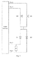
- Fig. 2 is a schematic diagram of an audio interface adapter device and an audio signal receiving apparatus according to a first embodiment of the present disclosure.
- the unidirectional conductive element is a diode
- the signal processing module comprises first and second signal processing units which are loudspeakers.
- the audio interface adapter device comprises an audio interface, a loudspeaker M1, a loudspeaker M2, a diode D1 and a diode D2.
- the audio interface comprises a pin 1, a pin 2, a pin 3 and a pin 4.
- the pin 1 and the pin 2 are used as an audio pin, and may be a left-channel pin and a right-channel pin respectively.
- the pin 3 may be used as an MIC pin and the pin 4 may be used as a ground pin.
- the pin 3 may be used as the ground pin, and the pin 4 may be used as the MIC pin.
- the audio interface of the present disclosure may be any four-section headphone plug or headphone jack, such as the headphone plug or headphone jack with a diameter of 3.5mm or 2.5mm.
- the pin 1 (the left-channel pin) and the pin 2 (the right-channel pin) of the audio interface are connected with a first end of the loudspeaker M1 and a first end of the loudspeaker M2 respectively, a second end of the loudspeaker M1 and a second end of the loudspeaker M2 are connected with an anode of the diode D1 and an anode of the diode D2, a cathode of the diode D1 and a cathode of the diode D2 are connected with the pin 3 and the pin 4 of the audio interface respectively.
- Each of the diode D1 and the diode D2 may be a germanium diode.
- the audio signal receiving apparatus of the present disclosure can be inserted into a headphone jack of an audio signal sending apparatus (for example, a smart phone) directly.
- the audio signal receiving apparatus of the present disclosure can be connected with the headphone jack of the smart phone via an adapter cable having two headphone plugs at two ends thereof.
- the audio signal receiving apparatus using the audio interface adapter device of the present disclosure may be a headphone, a headset, a loudspeaker, etc.
- the audio signal receiving apparatus When the audio signal receiving apparatus provided with the above audio interface adapter device is connected with the audio signal sending apparatus, no matter what type of the pin 3 and the pin 4 of the audio interface of the audio signal sending apparatus is, the audio signal receiving apparatus can pass the detection and identification performed for the pin 1 and the pin 2 (i.e. the audio pin) by the audio signal sending device successfully, and receive and process the audio signal using the pin 1 and the pin 2 normally.
- the audio signal receiving apparatus can pass the detection and identification performed for the pin 1 and the pin 2 (i.e. the audio pin) by the audio signal sending device successfully, and receive and process the audio signal using the pin 1 and the pin 2 normally.
- the pin 3 and the pin 4 can be connected via a bidirectional conductive element, for example, a resistor R1.
- a resistance of the above bidirectional conductive element ranges from 7.7K ⁇ to 15K ⁇ , and generally is 10 K ⁇ , 12 K ⁇ or 15 K ⁇ .
- the audio signal receiving apparatus of the present disclosure can pass the detection and identification for the MIC pin by the audio signal sending apparatus successfully.
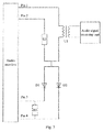
- Fig. 3 is a schematic diagram of an audio interface adapter device and an audio signal receiving apparatus according to a second embodiment of the present disclosure.
- the unidirectional conductive element is a diode
- the signal processing module comprises first and second signal processing units which are a resistor and a transformer U1 respectively.
- the difference between the second embodiment and the first embodiment is a different type of signal processing module.
- the signal processing unit connected with the pin 1 (or the pin 2) of the audio interface is the transformer
- the signal processing unit connected with the pin 2 (or the pin 1) of the audio interface is a resistor R2.
- the resistance of the resistor R2 is above 4 ⁇ , and generally is 8 ⁇ , 16 ⁇ , or 32 ⁇ .
- the pin 1 of the audio interface is connected with a first end of a primary coil of the transformer, and a second end of the primary coil is connected with the anode of the diode D1 and the anode of the diode D2 respectively.
- the audio signal receiving apparatus using the audio interface adapter device of this embodiment may further comprise an audio signal receiving unit.
- the audio signal receiving unit is connected with two ends of a secondary coil of the transformer, and configured to receive and an amplified audio signal and to process the amplified audio signal.
- the pin 1 and the pin 2 of the audio interface in this embodiment can be connected with the transformer U1 and a transformer U2 respectively.
- Two ends of the secondary coil of the transformer U1 and two ends of the secondary coil of the transformer U2 can be connected with one audio signal receiving unit or connected with two audio signal receiving units respectively.
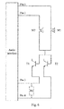
- Fig. 4 is a schematic diagram of an audio interface adapter device and an audio signal receiving apparatus according to a third embodiment of the present disclosure.
- the unidirectional conductive element is a diode
- the signal processing module comprises first and second signal processing units
- each of the first and second signal processing units comprises a resistor and a comparator connected in parallel.
- the difference between the third embodiment and the first embodiment is a different type of signal processing module.
- the signal processing unit connected with the pin 1 of the audio interface comprises a resistor R2 and a comparator C1 connected in parallel
- the signal processing unit connected with the pin 2 of the audio interface comprises a resistor R3 and a comparator C2 connected in parallel.
- the pin 1 is connected with a first terminal of the resistor R2 and a first input terminal (for example, a positive terminal) of the comparator C1, and a second terminal of the resistor R2 and a second input terminal (for example, a negative terminal) of the comparator C1 are connected with the anode of the diode D1 and the anode of the diode D2.
- the pin 2 is connected with a first terminal of the resistor R3 and a first input terminal (for example, a positive terminal) of the comparator C2 respectively, and a second terminal of the resistor R3 and a second input terminal (for example, a negative terminal) of the comparator C2 are connected with the anode of the diode D1 and the anode of the diode D2.
- the audio signal receiving apparatus using the audio interface adapter device of this embodiment may further comprise an audio signal receiving unit.
- the audio signal receiving unit is connected with an output terminal of the comparator C1 and an output terminal of the comparator C2 respectively, and configured to receive and process the audio signal processed by the comparator.
- the comparator in this embodiment may be an operational amplifier.
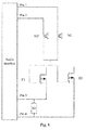
- Fig. 5 is a schematic diagram of an audio interface adapter device and an audio signal receiving apparatus according to a fourth embodiment of the present disclosure.
- the unidirectional conductive element is a PNP triode
- the signal processing module comprises first and second signal processing units which are loudspeakers.
- the difference between the fourth embodiment and the first embodiment is a different unidirectional conductive element.
- the unidirectional conductive elements comprise a triode T1 and a triode T2.
- An emitter of the triode T1 is connected with the pin 1 via a loudspeaker M1 and connected with the pin 2 via a loudspeaker M2, and a base of the triode T1 is connected with the pin 3.
- An emitter of the triode T2 is connected with the pin 1 via the loudspeaker M1 and connected with the pin 2 via the loudspeaker M2, and a base of the triode T2 is connected with the pin 4.
- Collectors of the triode T1 and the triode T2 can be suspended.
- the fourth embodiment is similar to the second embodiment and the third embodiment, and the first signal processing unit (the loudspeaker M1) and the second signal processing unit (the loudspeaker M2) in this embodiment may be the resistor and the transformer U1 respectively, or be the signal processing unit comprising a resistor and a comparator connected in parallel.
- Fig. 6 is a schematic diagram of an audio interface adapter device and an audio signal receiving apparatus according to a fifth embodiment of the present disclosure.
- the unidirectional conductive element is an NPN triode
- the signal processing module comprises first and second signal processing units which are loudspeakers.
- the difference between the fifth embodiment and the first embodiment is a different unidirectional conductive element.
- the unidirectional conductive elements comprise a triode T1 and a triode T2.
- a base of the triode T1 is connected with the pin 1 via the loudspeaker M1 and connected with the pin 2 via the loudspeaker M2, and an emitter of the triode T1 is connected with the pin 3.
- a base of the triode T2 is connected with the pin 1 via the loudspeaker M1 and connected with the pin 2 via the loudspeaker M2, and an emitter of the triode T2 is connected with the pin 4.
- Collectors of the triode T1 and the triode T2 can be suspended.
- the fifth embodiment is similar to the second embodiment and the third embodiment, and the first signal processing unit (the loudspeaker M1) and the second signal processing unit (the loudspeaker M2) in this embodiment may be the resistor and the transformer U1 respectively, or be the signal processing unit comprising a resistor and a comparator connected in parallel.
- Fig. 7 is a schematic diagram of an audio interface adapter device and an audio signal receiving apparatus according to a sixth embodiment of the present disclosure.
- the unidirectional conductive element is an N-channel junction MOS transistor
- the signal processing module comprises first and second signal processing units which are loudspeakers.
- the difference between the sixth embodiment and the first embodiment is a different unidirectional conductive element.
- the unidirectional conductive elements comprise a MOS transistor F1 and a MOS transistor F2.
- a source of the MOS transistor F1 is connected with the pin 1 via the loudspeaker M1 and connected with the pin 2 via the loudspeaker M2, and a gate of the MOS transistor F1 is connected with the pin 3.
- a source of the MOS transistor F2 is connected with the pin 1 via the loudspeaker M1 and connected with the pin 2 via the loudspeaker M2, and a gate of the MOS transistor F2 is connected with the pin 4.
- Drains of the MOS transistor F1 and the MOS transistor F2 can be suspended.
- the sixth embodiment is similar to the second embodiment and the third embodiment, and the first signal processing unit (the loudspeaker M1) and the second signal processing unit (the loudspeaker M2) in this embodiment may be the resistor and the transformer U1 respectively, or be the signal processing unit comprising a resistor and a comparator connected in parallel.
- Fig. 8 is a schematic diagram of an audio interface adapter device and an audio signal receiving apparatus according to a seventh embodiment of the present disclosure.
- the unidirectional conductive element is a P-channel junction MOS transistor
- the signal processing module comprises first and second signal processing units which are loudspeakers.
- the difference between the seventh embodiment and the first embodiment is a different unidirectional conductive element.
- the unidirectional conductive elements comprise a MOS transistor F1 and a MOS transistor F2.
- a gate of the MOS transistor F1 is connected with the pin 1 via the loudspeaker M1 and connected with the pin 2 via the loudspeaker M2, and a source of the MOS transistor F1 is connected with the pin 3.
- a gate of the MOS transistor F2 is connected with the pin 1 via the loudspeaker M1 and connected with the pin 2 via the loudspeaker M2, and a source of the MOS transistor F2 is connected with the pin 4.
- Drains of the MOS transistor F1 and the MOS transistor F2 can be suspended.
- the seventh embodiment is similar to the second embodiment and the third embodiment, and the first signal processing unit (the loudspeaker M1) and the second signal processing unit (the loudspeaker M2) in this embodiment may be the resistor and the transformer U1 respectively, or be the signal processing unit comprising a resistor and a comparator connected in parallel.
- the first unidirectional conductive element and the second unidirectional conductive element may be different types of elements, for example, the first unidirectional conductive element is a diode, and the second unidirectional conductive element is a triode.
- the pin 1 and the pin 2 of the audio interface are connected with the signal processing units via unidirectional conductive elements respectively.
- one of the pin 1 and the pin 2 is connected with the unidirectional conductive elements via the signal processing unit, and the other one of the pin 1 and the pin 2 is connected with the unidirectional conductive elements directly.
- first unidirectional conductive element and the second unidirectional conductive element can be integrated in a single chip, for example, the BAT54 chip.
Landscapes
- Physics & Mathematics (AREA)
- Engineering & Computer Science (AREA)
- Acoustics & Sound (AREA)
- Signal Processing (AREA)
- Health & Medical Sciences (AREA)
- General Health & Medical Sciences (AREA)
- Otolaryngology (AREA)
- Stereophonic Arrangements (AREA)
- Circuit For Audible Band Transducer (AREA)
- Amplifiers (AREA)
Applications Claiming Priority (2)
| Application Number | Priority Date | Filing Date | Title |
|---|---|---|---|
| CN201210016852.0A CN103220598B (zh) | 2012-01-18 | 2012-01-18 | 一种音频接口适配装置及音频信号接收设备 |
| PCT/CN2012/087889 WO2013107271A1 (zh) | 2012-01-18 | 2012-12-28 | 一种音频接口适配装置及音频信号接收设备 |
Publications (3)
| Publication Number | Publication Date |
|---|---|
| EP2806655A1 EP2806655A1 (en) | 2014-11-26 |
| EP2806655A4 EP2806655A4 (en) | 2015-07-29 |
| EP2806655B1 true EP2806655B1 (en) | 2016-09-14 |
Family
ID=48798601
Family Applications (1)
| Application Number | Title | Priority Date | Filing Date |
|---|---|---|---|
| EP12865732.7A Not-in-force EP2806655B1 (en) | 2012-01-18 | 2012-12-28 | Audio interface adapter device and audio signal receiving apparatus |
Country Status (6)
| Country | Link |
|---|---|
| US (1) | US9179216B2 (zh) |
| EP (1) | EP2806655B1 (zh) |
| CN (1) | CN103220598B (zh) |
| CA (1) | CA2845107C (zh) |
| HK (1) | HK1184945A1 (zh) |
| WO (1) | WO2013107271A1 (zh) |
Families Citing this family (4)
| Publication number | Priority date | Publication date | Assignee | Title |
|---|---|---|---|---|
| CN102883255B (zh) | 2012-09-13 | 2014-12-03 | 天地融科技股份有限公司 | 转接装置、电子签名工具、检测装置和接口检测系统 |
| CN106331948A (zh) * | 2015-07-01 | 2017-01-11 | 朗新科技股份有限公司 | 具有自适配功能的手机音频接口通信设备 |
| CN105430004A (zh) * | 2015-12-22 | 2016-03-23 | 上海爱信诺航芯电子科技有限公司 | 耳机接口标准的音频密码钥匙及接口适配方法 |
| US9872117B2 (en) * | 2016-03-01 | 2018-01-16 | Blackberry Limited | Device and method for adjusting an output to an audio port based on a determined sensitivity |
Family Cites Families (19)
| Publication number | Priority date | Publication date | Assignee | Title |
|---|---|---|---|---|
| TW527843B (en) * | 2002-02-15 | 2003-04-11 | High Tech Comp Corp | Earphone detecting circuit |
| US6856046B1 (en) * | 2002-03-08 | 2005-02-15 | Analog Devices, Inc. | Plug-in device discrimination circuit and method |
| TW595239B (en) * | 2003-01-28 | 2004-06-21 | Htc Corp | Detection circuit to detect the earphone type plugged into the insertion hole |
| JP4143635B2 (ja) * | 2005-10-26 | 2008-09-03 | Necインフロンティア株式会社 | オーディオ入出力装置および入出力機能切り替え方法 |
| KR20080038586A (ko) * | 2006-10-30 | 2008-05-07 | 전윤호 | 청력손실을 방지하기 위한 오디오 볼륨 조절 방법 및 장치 |
| CN201066840Y (zh) * | 2007-06-27 | 2008-05-28 | 青岛海信移动通信技术股份有限公司 | 具有耳机接口复用电路的移动手机 |
| US8362654B2 (en) * | 2007-11-21 | 2013-01-29 | Nokia Corporation | Electronic device interface switching system |
| JP4760903B2 (ja) * | 2008-12-26 | 2011-08-31 | ソニー株式会社 | 情報処理装置及び情報処理方法 |
| CN201438749U (zh) * | 2009-07-16 | 2010-04-14 | 萨基姆移动电话研发(宁波)有限公司 | 一种抑制音频设备开关杂音的电路 |
| CN101719610A (zh) * | 2009-12-30 | 2010-06-02 | 华为终端有限公司 | 一种有线耳机兼容方法和装置 |
| CN101841753A (zh) * | 2010-02-24 | 2010-09-22 | 深圳桑菲消费通信有限公司 | 一种用于便携式电子设备的线控耳机及其实现线控的方法 |
| CN201673685U (zh) * | 2010-06-03 | 2010-12-15 | 郭昊 | 一种适合高品质耳机的音频播放器 |
| CN102096651B (zh) * | 2010-12-22 | 2016-03-30 | 努比亚技术有限公司 | 基于标准Micro USB接口的手机接口复用电路 |
| CN102263347B (zh) * | 2011-06-15 | 2013-07-10 | 天地融科技股份有限公司 | 一种音频信号转接装置 |
| CN102300003B (zh) * | 2011-09-20 | 2013-12-11 | 惠州Tcl移动通信有限公司 | 一种自动检测耳机插口的移动终端 |
| US9319768B2 (en) * | 2011-12-06 | 2016-04-19 | Conexant Systems, Inc. | Multi-standard headset support with integrated ground switching |
| CN103379420B (zh) * | 2012-04-18 | 2016-10-05 | 华为终端有限公司 | 一种确定耳机线序的方法及电子设备 |
| CN102739183B (zh) * | 2012-06-13 | 2013-08-21 | 天地融科技股份有限公司 | 移动终端的音频接口匹配识别方法、装置和电子签名工具 |
| CN202721651U (zh) * | 2012-06-13 | 2013-02-06 | 天地融科技股份有限公司 | 移动终端的音频接口匹配识别装置和电子签名工具 |
-
2012
- 2012-01-18 CN CN201210016852.0A patent/CN103220598B/zh active Active
- 2012-12-28 US US14/347,433 patent/US9179216B2/en not_active Expired - Fee Related
- 2012-12-28 CA CA2845107A patent/CA2845107C/en active Active
- 2012-12-28 EP EP12865732.7A patent/EP2806655B1/en not_active Not-in-force
- 2012-12-28 WO PCT/CN2012/087889 patent/WO2013107271A1/zh active Application Filing
-
2013
- 2013-10-31 HK HK13112262.1A patent/HK1184945A1/zh unknown
Also Published As
| Publication number | Publication date |
|---|---|
| US9179216B2 (en) | 2015-11-03 |
| CN103220598B (zh) | 2016-03-30 |
| HK1184945A1 (zh) | 2014-01-30 |
| WO2013107271A1 (zh) | 2013-07-25 |
| CN103220598A (zh) | 2013-07-24 |
| EP2806655A4 (en) | 2015-07-29 |
| CA2845107A1 (en) | 2013-07-25 |
| US20150016624A1 (en) | 2015-01-15 |
| EP2806655A1 (en) | 2014-11-26 |
| CA2845107C (en) | 2016-10-04 |
Similar Documents
| Publication | Publication Date | Title |
|---|---|---|
| EP2863652B1 (en) | Audio interface self-adaptation device | |
| CA2854880C (en) | Apparatus for detecting type of audio interface | |
| CN104620567A (zh) | 用于检测在音频插头中的地线和麦克风输入触头的系统和方法 | |
| CN102457793B (zh) | 耳机接口电路及具有该耳机接口电路的电子装置 | |
| US9357297B2 (en) | Audio signal adapter device and system for transmitting audio signal | |
| EP2806655B1 (en) | Audio interface adapter device and audio signal receiving apparatus | |
| TW201218547A (en) | Earphone interface circuit and mobile phone using the same | |
| AU2013275897B2 (en) | Method, device, and electronic signature tool for use in matching with audio interface of mobile terminal | |
| WO2015182663A1 (ja) | 電子機器、イヤホン、および電子機器システム | |
| EP2871853A1 (en) | Identification device for matching audio interface of mobile terminal and electronic signature tool | |
| JP2016123041A (ja) | 電子機器 | |
| CN105979423B (zh) | 一种耳机上的麦克风的静音电路和方法 | |
| US20130108072A1 (en) | Wireless Device for Receiving and Forwarding an Audio Signal | |
| US20150208164A1 (en) | Downlink transmission device for audio signals and electronic signature token | |
| CN106331927B (zh) | 一种音频设备 | |
| JP6527795B2 (ja) | 電子機器 | |
| CN102375792A (zh) | 一种具有迷你usb接口的电子设备 |
Legal Events
| Date | Code | Title | Description |
|---|---|---|---|
| PUAI | Public reference made under article 153(3) epc to a published international application that has entered the european phase |
Free format text: ORIGINAL CODE: 0009012 |
|
| 17P | Request for examination filed |
Effective date: 20140331 |
|
| AK | Designated contracting states |
Kind code of ref document: A1 Designated state(s): AL AT BE BG CH CY CZ DE DK EE ES FI FR GB GR HR HU IE IS IT LI LT LU LV MC MK MT NL NO PL PT RO RS SE SI SK SM TR |
|
| DAX | Request for extension of the european patent (deleted) | ||
| RA4 | Supplementary search report drawn up and despatched (corrected) |
Effective date: 20150625 |
|
| RIC1 | Information provided on ipc code assigned before grant |
Ipc: H04R 29/00 20060101ALI20150619BHEP Ipc: H04R 3/00 20060101AFI20150619BHEP Ipc: G06F 3/16 20060101ALI20150619BHEP |
|
| GRAP | Despatch of communication of intention to grant a patent |
Free format text: ORIGINAL CODE: EPIDOSNIGR1 |
|
| RIC1 | Information provided on ipc code assigned before grant |
Ipc: H04R 29/00 20060101ALI20160330BHEP Ipc: G06F 3/16 20060101ALI20160330BHEP Ipc: H04R 3/00 20060101AFI20160330BHEP |
|
| INTG | Intention to grant announced |
Effective date: 20160420 |
|
| GRAS | Grant fee paid |
Free format text: ORIGINAL CODE: EPIDOSNIGR3 |
|
| GRAA | (expected) grant |
Free format text: ORIGINAL CODE: 0009210 |
|
| AK | Designated contracting states |
Kind code of ref document: B1 Designated state(s): AL AT BE BG CH CY CZ DE DK EE ES FI FR GB GR HR HU IE IS IT LI LT LU LV MC MK MT NL NO PL PT RO RS SE SI SK SM TR |
|
| REG | Reference to a national code |
Ref country code: GB Ref legal event code: FG4D |
|
| REG | Reference to a national code |
Ref country code: CH Ref legal event code: EP |
|
| REG | Reference to a national code |
Ref country code: IE Ref legal event code: FG4D |
|
| REG | Reference to a national code |
Ref country code: AT Ref legal event code: REF Ref document number: 830134 Country of ref document: AT Kind code of ref document: T Effective date: 20161015 |
|
| REG | Reference to a national code |
Ref country code: DE Ref legal event code: R096 Ref document number: 602012023181 Country of ref document: DE |
|
| REG | Reference to a national code |
Ref country code: LT Ref legal event code: MG4D |
|
| REG | Reference to a national code |
Ref country code: NL Ref legal event code: MP Effective date: 20160914 |
|
| PG25 | Lapsed in a contracting state [announced via postgrant information from national office to epo] |
Ref country code: NO Free format text: LAPSE BECAUSE OF FAILURE TO SUBMIT A TRANSLATION OF THE DESCRIPTION OR TO PAY THE FEE WITHIN THE PRESCRIBED TIME-LIMIT Effective date: 20161214 Ref country code: HR Free format text: LAPSE BECAUSE OF FAILURE TO SUBMIT A TRANSLATION OF THE DESCRIPTION OR TO PAY THE FEE WITHIN THE PRESCRIBED TIME-LIMIT Effective date: 20160914 Ref country code: LT Free format text: LAPSE BECAUSE OF FAILURE TO SUBMIT A TRANSLATION OF THE DESCRIPTION OR TO PAY THE FEE WITHIN THE PRESCRIBED TIME-LIMIT Effective date: 20160914 Ref country code: RS Free format text: LAPSE BECAUSE OF FAILURE TO SUBMIT A TRANSLATION OF THE DESCRIPTION OR TO PAY THE FEE WITHIN THE PRESCRIBED TIME-LIMIT Effective date: 20160914 Ref country code: FI Free format text: LAPSE BECAUSE OF FAILURE TO SUBMIT A TRANSLATION OF THE DESCRIPTION OR TO PAY THE FEE WITHIN THE PRESCRIBED TIME-LIMIT Effective date: 20160914 |
|
| REG | Reference to a national code |
Ref country code: AT Ref legal event code: MK05 Ref document number: 830134 Country of ref document: AT Kind code of ref document: T Effective date: 20160914 |
|
| PG25 | Lapsed in a contracting state [announced via postgrant information from national office to epo] |
Ref country code: LV Free format text: LAPSE BECAUSE OF FAILURE TO SUBMIT A TRANSLATION OF THE DESCRIPTION OR TO PAY THE FEE WITHIN THE PRESCRIBED TIME-LIMIT Effective date: 20160914 Ref country code: GR Free format text: LAPSE BECAUSE OF FAILURE TO SUBMIT A TRANSLATION OF THE DESCRIPTION OR TO PAY THE FEE WITHIN THE PRESCRIBED TIME-LIMIT Effective date: 20161215 Ref country code: NL Free format text: LAPSE BECAUSE OF FAILURE TO SUBMIT A TRANSLATION OF THE DESCRIPTION OR TO PAY THE FEE WITHIN THE PRESCRIBED TIME-LIMIT Effective date: 20160914 Ref country code: SE Free format text: LAPSE BECAUSE OF FAILURE TO SUBMIT A TRANSLATION OF THE DESCRIPTION OR TO PAY THE FEE WITHIN THE PRESCRIBED TIME-LIMIT Effective date: 20160914 |
|
| PG25 | Lapsed in a contracting state [announced via postgrant information from national office to epo] |
Ref country code: RO Free format text: LAPSE BECAUSE OF FAILURE TO SUBMIT A TRANSLATION OF THE DESCRIPTION OR TO PAY THE FEE WITHIN THE PRESCRIBED TIME-LIMIT Effective date: 20160914 Ref country code: EE Free format text: LAPSE BECAUSE OF FAILURE TO SUBMIT A TRANSLATION OF THE DESCRIPTION OR TO PAY THE FEE WITHIN THE PRESCRIBED TIME-LIMIT Effective date: 20160914 |
|
| PG25 | Lapsed in a contracting state [announced via postgrant information from national office to epo] |
Ref country code: PT Free format text: LAPSE BECAUSE OF FAILURE TO SUBMIT A TRANSLATION OF THE DESCRIPTION OR TO PAY THE FEE WITHIN THE PRESCRIBED TIME-LIMIT Effective date: 20170116 Ref country code: AT Free format text: LAPSE BECAUSE OF FAILURE TO SUBMIT A TRANSLATION OF THE DESCRIPTION OR TO PAY THE FEE WITHIN THE PRESCRIBED TIME-LIMIT Effective date: 20160914 Ref country code: SK Free format text: LAPSE BECAUSE OF FAILURE TO SUBMIT A TRANSLATION OF THE DESCRIPTION OR TO PAY THE FEE WITHIN THE PRESCRIBED TIME-LIMIT Effective date: 20160914 Ref country code: ES Free format text: LAPSE BECAUSE OF FAILURE TO SUBMIT A TRANSLATION OF THE DESCRIPTION OR TO PAY THE FEE WITHIN THE PRESCRIBED TIME-LIMIT Effective date: 20160914 Ref country code: BG Free format text: LAPSE BECAUSE OF FAILURE TO SUBMIT A TRANSLATION OF THE DESCRIPTION OR TO PAY THE FEE WITHIN THE PRESCRIBED TIME-LIMIT Effective date: 20161214 Ref country code: SM Free format text: LAPSE BECAUSE OF FAILURE TO SUBMIT A TRANSLATION OF THE DESCRIPTION OR TO PAY THE FEE WITHIN THE PRESCRIBED TIME-LIMIT Effective date: 20160914 Ref country code: PL Free format text: LAPSE BECAUSE OF FAILURE TO SUBMIT A TRANSLATION OF THE DESCRIPTION OR TO PAY THE FEE WITHIN THE PRESCRIBED TIME-LIMIT Effective date: 20160914 Ref country code: BE Free format text: LAPSE BECAUSE OF FAILURE TO SUBMIT A TRANSLATION OF THE DESCRIPTION OR TO PAY THE FEE WITHIN THE PRESCRIBED TIME-LIMIT Effective date: 20160914 Ref country code: CZ Free format text: LAPSE BECAUSE OF FAILURE TO SUBMIT A TRANSLATION OF THE DESCRIPTION OR TO PAY THE FEE WITHIN THE PRESCRIBED TIME-LIMIT Effective date: 20160914 Ref country code: IS Free format text: LAPSE BECAUSE OF FAILURE TO SUBMIT A TRANSLATION OF THE DESCRIPTION OR TO PAY THE FEE WITHIN THE PRESCRIBED TIME-LIMIT Effective date: 20170114 |
|
| REG | Reference to a national code |
Ref country code: DE Ref legal event code: R097 Ref document number: 602012023181 Country of ref document: DE |
|
| PG25 | Lapsed in a contracting state [announced via postgrant information from national office to epo] |
Ref country code: IT Free format text: LAPSE BECAUSE OF FAILURE TO SUBMIT A TRANSLATION OF THE DESCRIPTION OR TO PAY THE FEE WITHIN THE PRESCRIBED TIME-LIMIT Effective date: 20160914 |
|
| PLBE | No opposition filed within time limit |
Free format text: ORIGINAL CODE: 0009261 |
|
| STAA | Information on the status of an ep patent application or granted ep patent |
Free format text: STATUS: NO OPPOSITION FILED WITHIN TIME LIMIT |
|
| PG25 | Lapsed in a contracting state [announced via postgrant information from national office to epo] |
Ref country code: DK Free format text: LAPSE BECAUSE OF FAILURE TO SUBMIT A TRANSLATION OF THE DESCRIPTION OR TO PAY THE FEE WITHIN THE PRESCRIBED TIME-LIMIT Effective date: 20160914 |
|
| REG | Reference to a national code |
Ref country code: CH Ref legal event code: PL |
|
| 26N | No opposition filed |
Effective date: 20170615 |
|
| GBPC | Gb: european patent ceased through non-payment of renewal fee |
Effective date: 20161228 |
|
| PG25 | Lapsed in a contracting state [announced via postgrant information from national office to epo] |
Ref country code: MC Free format text: LAPSE BECAUSE OF FAILURE TO SUBMIT A TRANSLATION OF THE DESCRIPTION OR TO PAY THE FEE WITHIN THE PRESCRIBED TIME-LIMIT Effective date: 20160914 |
|
| REG | Reference to a national code |
Ref country code: FR Ref legal event code: ST Effective date: 20170831 |
|
| PG25 | Lapsed in a contracting state [announced via postgrant information from national office to epo] |
Ref country code: LI Free format text: LAPSE BECAUSE OF NON-PAYMENT OF DUE FEES Effective date: 20161231 Ref country code: LU Free format text: LAPSE BECAUSE OF NON-PAYMENT OF DUE FEES Effective date: 20161228 Ref country code: CH Free format text: LAPSE BECAUSE OF NON-PAYMENT OF DUE FEES Effective date: 20161231 Ref country code: FR Free format text: LAPSE BECAUSE OF NON-PAYMENT OF DUE FEES Effective date: 20170102 |
|
| PG25 | Lapsed in a contracting state [announced via postgrant information from national office to epo] |
Ref country code: GB Free format text: LAPSE BECAUSE OF NON-PAYMENT OF DUE FEES Effective date: 20161228 Ref country code: SI Free format text: LAPSE BECAUSE OF FAILURE TO SUBMIT A TRANSLATION OF THE DESCRIPTION OR TO PAY THE FEE WITHIN THE PRESCRIBED TIME-LIMIT Effective date: 20160914 |
|
| PG25 | Lapsed in a contracting state [announced via postgrant information from national office to epo] |
Ref country code: HU Free format text: LAPSE BECAUSE OF FAILURE TO SUBMIT A TRANSLATION OF THE DESCRIPTION OR TO PAY THE FEE WITHIN THE PRESCRIBED TIME-LIMIT; INVALID AB INITIO Effective date: 20121228 |
|
| PG25 | Lapsed in a contracting state [announced via postgrant information from national office to epo] |
Ref country code: CY Free format text: LAPSE BECAUSE OF FAILURE TO SUBMIT A TRANSLATION OF THE DESCRIPTION OR TO PAY THE FEE WITHIN THE PRESCRIBED TIME-LIMIT Effective date: 20160914 Ref country code: MK Free format text: LAPSE BECAUSE OF FAILURE TO SUBMIT A TRANSLATION OF THE DESCRIPTION OR TO PAY THE FEE WITHIN THE PRESCRIBED TIME-LIMIT Effective date: 20160914 |
|
| PG25 | Lapsed in a contracting state [announced via postgrant information from national office to epo] |
Ref country code: MT Free format text: LAPSE BECAUSE OF NON-PAYMENT OF DUE FEES Effective date: 20161228 |
|
| PG25 | Lapsed in a contracting state [announced via postgrant information from national office to epo] |
Ref country code: TR Free format text: LAPSE BECAUSE OF FAILURE TO SUBMIT A TRANSLATION OF THE DESCRIPTION OR TO PAY THE FEE WITHIN THE PRESCRIBED TIME-LIMIT Effective date: 20160914 Ref country code: AL Free format text: LAPSE BECAUSE OF FAILURE TO SUBMIT A TRANSLATION OF THE DESCRIPTION OR TO PAY THE FEE WITHIN THE PRESCRIBED TIME-LIMIT Effective date: 20160914 |
|
| PGFP | Annual fee paid to national office [announced via postgrant information from national office to epo] |
Ref country code: DE Payment date: 20211210 Year of fee payment: 10 Ref country code: IE Payment date: 20211122 Year of fee payment: 10 |
|
| REG | Reference to a national code |
Ref country code: DE Ref legal event code: R119 Ref document number: 602012023181 Country of ref document: DE |
|
| PG25 | Lapsed in a contracting state [announced via postgrant information from national office to epo] |
Ref country code: IE Free format text: LAPSE BECAUSE OF NON-PAYMENT OF DUE FEES Effective date: 20221228 Ref country code: DE Free format text: LAPSE BECAUSE OF NON-PAYMENT OF DUE FEES Effective date: 20230701 |