EP2806460B1 - Halbleitervorrichtung und Schaltung mit dynamischer Steuerung des elektrischen Feldes - Google Patents
Halbleitervorrichtung und Schaltung mit dynamischer Steuerung des elektrischen Feldes Download PDFInfo
- Publication number
- EP2806460B1 EP2806460B1 EP14169718.5A EP14169718A EP2806460B1 EP 2806460 B1 EP2806460 B1 EP 2806460B1 EP 14169718 A EP14169718 A EP 14169718A EP 2806460 B1 EP2806460 B1 EP 2806460B1
- Authority
- EP
- European Patent Office
- Prior art keywords
- semiconductor device
- circuit
- collector
- transistor
- voltage
- Prior art date
- Legal status (The legal status is an assumption and is not a legal conclusion. Google has not performed a legal analysis and makes no representation as to the accuracy of the status listed.)
- Active
Links
Images



Classifications
-
- H—ELECTRICITY
- H03—ELECTRONIC CIRCUITRY
- H03K—PULSE TECHNIQUE
- H03K17/00—Electronic switching or gating, i.e. not by contact-making and –breaking
- H03K17/10—Modifications for increasing the maximum permissible switched voltage
-
- G—PHYSICS
- G05—CONTROLLING; REGULATING
- G05F—SYSTEMS FOR REGULATING ELECTRIC OR MAGNETIC VARIABLES
- G05F1/00—Automatic systems in which deviations of an electric quantity from one or more predetermined values are detected at the output of the system and fed back to a device within the system to restore the detected quantity to its predetermined value or values, i.e. retroactive systems
- G05F1/10—Regulating voltage or current
- G05F1/46—Regulating voltage or current wherein the variable actually regulated by the final control device is DC
- G05F1/462—Regulating voltage or current wherein the variable actually regulated by the final control device is DC as a function of the requirements of the load, e.g. delay, temperature, specific voltage/current characteristic
-
- H—ELECTRICITY
- H03—ELECTRONIC CIRCUITRY
- H03F—AMPLIFIERS
- H03F3/00—Amplifiers with only discharge tubes or only semiconductor devices as amplifying elements
- H03F3/189—High-frequency amplifiers, e.g. radio frequency amplifiers
- H03F3/19—High-frequency amplifiers, e.g. radio frequency amplifiers with semiconductor devices only
-
- H—ELECTRICITY
- H03—ELECTRONIC CIRCUITRY
- H03F—AMPLIFIERS
- H03F3/00—Amplifiers with only discharge tubes or only semiconductor devices as amplifying elements
- H03F3/20—Power amplifiers, e.g. Class B amplifiers, Class C amplifiers
- H03F3/21—Power amplifiers, e.g. Class B amplifiers, Class C amplifiers with semiconductor devices only
-
- H—ELECTRICITY
- H10—SEMICONDUCTOR DEVICES; ELECTRIC SOLID-STATE DEVICES NOT OTHERWISE PROVIDED FOR
- H10D—INORGANIC ELECTRIC SEMICONDUCTOR DEVICES
- H10D10/00—Bipolar junction transistors [BJT]
- H10D10/40—Vertical BJTs
- H10D10/461—Inverted vertical BJTs
-
- H—ELECTRICITY
- H10—SEMICONDUCTOR DEVICES; ELECTRIC SOLID-STATE DEVICES NOT OTHERWISE PROVIDED FOR
- H10D—INORGANIC ELECTRIC SEMICONDUCTOR DEVICES
- H10D10/00—Bipolar junction transistors [BJT]
- H10D10/80—Heterojunction BJTs
-
- H—ELECTRICITY
- H10—SEMICONDUCTOR DEVICES; ELECTRIC SOLID-STATE DEVICES NOT OTHERWISE PROVIDED FOR
- H10D—INORGANIC ELECTRIC SEMICONDUCTOR DEVICES
- H10D62/00—Semiconductor bodies, or regions thereof, of devices having potential barriers
- H10D62/80—Semiconductor bodies, or regions thereof, of devices having potential barriers characterised by the materials
- H10D62/82—Heterojunctions
- H10D62/822—Heterojunctions comprising only Group IV materials heterojunctions, e.g. Si/Ge heterojunctions
-
- H—ELECTRICITY
- H10—SEMICONDUCTOR DEVICES; ELECTRIC SOLID-STATE DEVICES NOT OTHERWISE PROVIDED FOR
- H10D—INORGANIC ELECTRIC SEMICONDUCTOR DEVICES
- H10D64/00—Electrodes of devices having potential barriers
- H10D64/111—Field plates
-
- H—ELECTRICITY
- H03—ELECTRONIC CIRCUITRY
- H03F—AMPLIFIERS
- H03F1/00—Details of amplifiers with only discharge tubes, only semiconductor devices or only unspecified devices as amplifying elements
- H03F1/34—Negative-feedback-circuit arrangements with or without positive feedback
-
- H—ELECTRICITY
- H03—ELECTRONIC CIRCUITRY
- H03F—AMPLIFIERS
- H03F2200/00—Indexing scheme relating to amplifiers
- H03F2200/153—Feedback used to stabilise the amplifier
Definitions
- This invention relates to a circuit including a semiconductor device such as transistors and diodes and, in particular, bipolar transistors, which make use of a control terminal (additional to the base, collector and emitter terminals, for example), for controlling the electric field distribution within a portion of the device.
- a semiconductor device such as transistors and diodes and, in particular, bipolar transistors, which make use of a control terminal (additional to the base, collector and emitter terminals, for example), for controlling the electric field distribution within a portion of the device.
- CMOS based technologies can be used to produce high output power amplifiers
- bipolar technologies remain important for providing high-efficiency, high power amplifiers at (ultra-) high frequencies. There is often a trade-off in bipolar devices between high power performance, high frequency performance and cost.
- US 2013/0126945 and CN 102437180 disclose an ultra high voltage silicon-germanium (SiGe) heterojunction bipolar transistor (HBT), in which a collector region is formed between two isolation structures; a pseudo buried layer is formed under each isolation structure and each side of the collector region is connected with a corresponding pseudo buried layer; a SiGe field plate is formed on each of the isolation structures; each pseudo buried layer is picked up by a first contact hole electrode and each SiGe field plate is picked up by a second contact hole electrode; and each first contact hole electrode is connected to its adjacent second contact hole electrode and the two contact hole electrodes jointly serve as an emitter.
- SiGe silicon-germanium
- HBT heterojunction bipolar transistor
- the structure described has a drift region, and one or more gate contacts, which enable shaping of the electric field in the drift region proximal to an active part of the device (e.g. base emitter region for a bipolar device or a channel region for a MOS-type device).
- an active part of the device e.g. base emitter region for a bipolar device or a channel region for a MOS-type device.
- This enables a uniform electric field to be shaped which enables the range over which the field is constant to be varied.
- the setting point for the trade-off between various device characteristics can be set.
- the electric field can be dynamically shaped, in real-time, to achieve advantageous semiconductor device performance.
- the structure described has a drift region, and one or more gate contacts, which enable shaping of the electric field in the collector region proximal to the base region. This enables a uniform electric field to be shaped enables the range over which the field is constant to be varied. As such the setting point for the trade-off between various bipolar transistor characteristics can be set.
- a circuit comprising:
- the ability to provide different transistor characteristics by dynamically setting a control voltage enables the performance of the semiconductor device to be modified in real time.
- the dynamic or "real-time" control or biasing can be applied to the gate terminal or terminals and follow another time-dependent signal such as an output voltage swing signal, a power envelope signal or any other time varying signal.
- the real-time modification of the bias voltage during operation of the semiconductor device is advantageous.
- BV breakdown voltage
- fMAX cut-off frequency
- fa any other RF parameter which describes the speed of the device depending on the type of application, e.g. fMAX, fa
- the control voltage on the field-shaping part of the transistor (e.g. the gate(s)) being dynamically controlled in real-time, i.e. the voltage at the gate is directly related to the voltage at another node of the device or circuit at any point in time during the RF operation is advantageous.
- the power capability/performance of the device can be extended during the RF operation by pushing or optimizing the load line outwards depending on the current-voltage combination that the transistor experiences at that particular point in time of the RF swing so that both the maximum voltage (such as VCE,MAX) and maximum current (such as I C,MAX ) can be increased.
- the circuit can be tuned to a particular application or even to a particular operation condition depending on the actual RF swing at the drift region by selecting the bias voltage under dynamic, real-time conditions.
- the semiconductor device may comprise a transistor, such as a bipolar junction transistor or MOS transistor (LDMOS or EDMOS for example).
- the semiconductor device may comprise a diode.
- the transistor may have a plurality of terminals and the field gate terminal or terminals for dynamically controlling the electric field in the drift region or active region of the transistor.
- the transistor may comprise a bipolar transistor and comprise a base, collector and emitter terminal and the field gate terminal or terminals may be configured to dynamically control the electric field in a collector region (which comprises the drift region).
- the dynamic control may be in dependence on a collector-emitter or base-emitter voltage of the bipolar transistor.
- the transistor such as a FET, may include a source, drain and gate terminal and the field gate terminal may be configured to dynamically control the electric field in a channel region (which comprises the drift region).
- the time-varying signal used by the feedback circuit to control the bias voltage may comprise a collector-emitter voltage if the semiconductor device comprises a bipolar transistor or a source-drain voltage if the semiconductor device is of MOS-type or an output voltage to the circuit. If the semiconductor device comprises a diode, a time-varying voltage applied to a terminal of the diode may be used.
- the feedback circuit comprises an inverter connected between an output of the semiconductor device and the field gate terminal configured to generate a bias voltage which relates to the time-varying signal.
- a high breakdown for reliable high voltage operation
- high current for smaller collector emitter voltage
- breakdown voltage comprises the maximum voltage at which the transistor is still capable of reliable operation.
- the feedback circuit may be configured to determine the bias voltage or voltages based on a time varying load mismatch signal. This is advantageous as a further node can be provided from which a time-varying signal of load mismatch can be derived and the feedback circuit may dynamically control the bias voltage(s) applied to the semiconductor device.
- the dynamic real-time control is preferably at the frequency of operation (or a derivative of the frequency of operation) of the device so that it can respond dynamically to the load conditions.
- the circuit may be used in an RF power amplifier.
- the invention also provides a method of controlling a semiconductor device comprising one or more field gate terminals for controlling the electric field in a drift region of the semiconductor device, the method comprising: dynamically controlling a bias voltage or bias voltages applied to the field gate terminal or terminals to achieve different transistor characteristics in real-time in response to a time-varying signal at a further node in the circuit; wherein the method further comprises generating the bias voltage or voltages that relate to the time-varying an inverter connected between an output of the semiconductor device and the field gate terminal.
- a transistor circuit comprising: a bipolar transistor comprising a base, collector and emitter, and at least one gate terminal for controlling the electric field in a collector region of the transistor; a control circuit for controlling a bias voltage applied to the gate terminal, with different control voltages used for different transistor characteristics.
- the circuit optionally comprising: at least first and second first transistor circuits, wherein the transistors of the first and second first transistor circuits are identical and have different bias voltages applied to them to achieve different transistor characteristics.
- the circuit comprising a feedback circuit for dynamically controlling a bias voltage applied to the gate terminal in dependence on a collector emitter voltage of the bipolar transistor.
- the feedback circuit comprises an inverter connected between the collector and gate terminal.
- the dynamic control is at the frequency of operation of the bipolar transistor.
- the circuit comprises an RF power amplifier.
- a method of controlling a bipolar transistor comprising a base, collector and emitter, and one gate terminal for controlling the electric field in a collector region of the transistor, wherein the method comprises: controlling a bias voltage applied to the gate terminal to achieve different transistor characteristics.
- the bias voltage is generated by an inverter connected between the collector region of the transistor and the gate terminal.
- the method comprises controlling first and second first transistor circuits, wherein the transistors of the first and second first transistor circuits are identical, and the method comprises applying different bias voltages to the transistor of the first and second first transistor circuits to achieve different transistor characteristics.
- the method comprises dynamically controlling a bias voltage applied to the gate terminal in dependence on a collector emitter voltage of the bipolar transistor.
- the dynamic control is at the frequency of operation of the bipolar transistor.
- the invention provides a circuit comprising a semiconductor device, which may, in one embodiment, comprise a transistor such as a bipolar transistor.
- the semiconductor device comprises a bipolar transistor having one or more gate terminals for dynamically controlling the electric field in a collector region of the transistor in real time.
- the bias voltage or voltages applied to the gate terminal or terminals are dynamically controlled to achieve different transistor characteristics based on a time varying variable of the circuit.
- MOS-type transistors e.g. LDMOS, EDMOS etc
- diodes e.g. LDMOS, EDMOS etc
- control is static, so that different identical transistors in a circuit can have different (fixed) characteristics.
- a feedback circuit dynamically controls a bias voltage applied to the field gate terminal in dependence on an output voltage or collector-emitter voltage or an input voltage or base-emitter voltage of the transistor. This enables the transistor performance to be tuned in real time to the dynamically varying collector voltages (i.e. electric fields) or load requirements.
- High-voltage devices such as Bipolar (or heterojunction bipolar) transistors
- Bipolar or heterojunction bipolar transistors
- a high-breakdown device is usually preferred allowing high voltage swing at the output (for high output power).
- high voltage devices usually have their limitations, which include:
- Figure 2 shows one example of bipolar transistor structure to which the invention can be applied.
- the method of the invention of using an extra terminal (for example to dynamically extend the power capability of the device in real-time) can be applied to any device provided there is a terminal or field plate that is coupled to the drift region of the device for modification of the field.
- the structure of Figure 2 is one example.
- the transistor has an emitter E, a base B and a collector C.
- the emitter E is formed in the bulk of the substrate of the device.
- the emitter E could also be formed as a layer above the surface of the substrate.
- the base B is provided as a layer of semiconductor material over the emitter E.
- the layer forming the base B can be deposited and patterned using standard lithographic techniques, to provide the desired dimensions and alignment with respect to the emitter E.
- the collector C can also be provided as a patterned layer of semiconductor material, dimensioned and aligned with respect to the base as desired.
- the collector C extends laterally in a plane substantially parallel to the major surface of the substrate.
- the collector C overlaps the base B (thereby to make contact therewith), but also extends past an edge of the base B and away from the overlapping region.
- a dielectric 10 is provided beneath the overhang portion of the collector C to ensure that this portion of the collector C does not make contact with the emitter E.
- the collector C is formed at the "top" of the device (i.e. above the emitter E and the base B).
- the emitter E, base B and collector C are each provided with corresponding emitter contact(s) 12, base contact(s) 14 and collector contact(s) 16
- the collector C is provided with a field gate comprising collector gate 18.
- the purpose of the collector gate 18 is to shape the electric field within the collector C.
- the collector gate is thus a field gate terminal of the device, in addition to the conventional base, emitter and collector terminals. It functions as a field plate. In this way, the peak electric field within the collector C can be dynamically suppressed, thereby improving still further the breakdown voltage of the device.
- This field shaping in this device thus makes use of a collector gate in a bottom-up bipolar transistor having a lateral collector.
- the gate can also be extended laterally over the entire collector region. This can give improved field shaping. It will be appreciated that any other field-plate configuration can be included.
- This invention relates to biasing of the field gate, and it can be applied to different transistor designs, such as vertical transistors. It can be applied to any structure which implements a field gate to enable field shaping in the drift region.
- a field plate can be used to reshape the field distribution.
- an accumulation layer can be formed under the field plate, which can be used for enhancing fr and current.
- the transistor has two main important figures of merit: breakdown voltages (BVcbo) and cut-off frequency (fT). While BVcbo is determined at the OFF-state condition, fT is determined at ON-state condition.
- BVcbo breakdown voltages
- Ft cut-off frequency
- a first application is to create a single design of device with various values of fr and breakdown voltage. This can be considered to be a static implementation not forming part of the invention, in which different transistors in a multiple-transistor circuit are biased to provide different transistor characteristics.
- one device can be made with an fr and breakdown (BVceo and BVcbo), which can be adjusted by varying only the field-plate bias.
- fr and breakdown BVceo and BVcbo
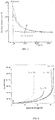
- Figure 5 shows an adjustable fr /BVceo with varied field-plate voltages.
- the breakdown voltage and fr and f MAX can be adapted (with fT and f MAX going up when BV is going down).
- the same design of device can be used either as a lower-frequency-higher-voltage device or as a high-frequency-lower-voltage device.
- a DC bias is applied to the gate which can be a single gate or a gate which is by split into parts.
- One or more gates can be used for optimal field shaping.
- a gate part closer to the base-collector junction can be used to shape the field for control of the breakdown.
- Different gates can be provided with different static bias levels.
- the supply voltages can be as high as 5V or 9V, while frequency bands are 900MHz, 2.1 GHz, 2.4 GHz, 3.5 GHz and 5.8GHz.
- the technology using gated devices such as the HBT of the example can cover:
- a further application in accordance with the invention is to enable selection of a particular load line for devices in a dynamic or real time way based on a time varying signal of the circuit.
- the power capability (and also linearity) of power amplifiers is determined by the maximum voltage (e.g. BVceo or BVcbo in a bipolar transistor) and maximum current.
- Figure 6 shows how the load line can be shifted by biasing the field-plate in real-time (at the same speed as collector).
- the desired load line can be selected by the dynamic switching approach. With a better load line, better linearity, output power or efficiency can be obtained as well.
- Region I a first region where a high breakdown is needed, a small V G is applied and a high reliable breakdown voltage (such as BVceo and also BVcbo) can be obtained.
- Region II a second region where a high current is needed, a large V G is applied (breakdown is not important here).
- FIG. 6 shows two load lines 30,32.
- the original load line is shown as 30 and the improved load line under dynamic or real time switching is shown as 32.
- the biasing does not change the load line, instead the load line is a choice made by the designer.
- the designer chooses a load which fits the requirements and generates enough power and linearity.
- This means that the loadline is fixed and determined by the load impedance, e.g. loadline 30.
- the loadline 32 crosses the breakdown voltage limit (V,MAX on x axis) and the maximum current (JMAX on y axis).
- the dynamic real-time control of the invention enables the designer not to be constrained by the maximum voltage and maximum current, so that a load impedance can be used that gives loadline 32, even if the breakdown voltage or maximum current of the transistor is lower than the corresponding V,MAX and JMAX.
- the transistor can be tuned to allow more current or voltage if the transistor is kept in the correct position on the loadline.
- the designer can only use load line 30 because of the maximum V,max and Jmax values.
- the dynamic real-time biasing approach enables the designer to use load line 32 because with the circuit operated with the correct dynamic biasing, both V,max and Jmax will shift, and the transistor will adapt its point of operation in real time to remain at a suitable point on the selected loadline.
- the power and linearity performance of power amplifiers is limited by Jmax and V,max (of the transistor).
- the invention enables both Jmax and V,max to be increased.
- the power and linearity performance of the power amplifier by enabling the user of load line 32 will be better than when there is only the choice of load line 30
- This way of biasing the field plate means the power capability of the device can be extended by pushing the load line further to the right hand side, i.e. both V ,MAX and I ,MAX can be increased.
- This enhancement is a large advantage to the current status of power (high-voltage) devices, where I MAX is often traded off versus V MAX .
- V G can be regulated so that whenever the power amplifier transistor experiences a high V out (peak-to-peak), the high output voltage can be detected and V G can be reduced in order to increase the breakdown voltage.
- the dynamic switching method can be used with detection of the mismatch case, and immediately the gate voltage can be lowered. In this way, a higher BV can be tolerated, whereas in normal situations, we can a higher VG is used. Thus, real time control of the bias voltage is advantageous.
- FIG. 7 An example of implementing dynamic real-time switching operation in a power amplifier is shown schematically in Figure 7 .
- Figure 7 shows the power transistor 40 with the field plate gate G.
- a substrate contact is also possible, but not essential.
- the (complex) load 42 is connected to the collector via a DC blocking capacitor 44.
- the transistor base is DC biased by a bias circuit 47 and the RF input is supplied through a decoupling capacitor 48.
- a choke inductor 49 is connected between the power supply line and the transistor 40.
- the choke 49 is used for decoupling DC and AC signals.
- the gate biasing is implemented by a high-speed inverter 46 which probes the collector-emitter voltage of the power transistor in real-time and sends this inverted signal to the gate of transistor 40.
- the gate biasing is low in the case of a high V CE (region I in Figure 6 ) while it is high for low V CE (region II in Figure 6 ).
- the collector forms further node from which the time-varying signal is received.
- the base-collector voltage can also be used as the feedback parameter.
- the base current can be probed or the voltage swing. Since there is a relation between base and collector current and voltages, probing the base could also be used to bias the gate.
- Sensing the output signal in a real-time mode for power amplifiers at high frequencies (GHz range) has been demonstrated for example in Young-Sang Jeon et al., "High-Efficiency Power Amplifier Using Novel Dynamic Bias Switching", IEEE Transactions of Microwave Theory and Techniques, vol. 55, No. 4, April 2007 for class-E type operation.
- the gate can be physically split in one or more sections ( i.e. more gates next to each other on the same collector region) with every section individually dynamically biased (although a subset may be static biased) depending on the application requirements or device operation.
- the invention thus provides an approach for dynamically biasing the field plate of bipolar devices to enable a dynamic real time change (i.e. adjustability) of device characteristics and their trade-off such as breakdown voltage (BVcbo/BVceo) vs. frequency ( f T lf MAX ).
- BVcbo/BVceo breakdown voltage
- f T lf MAX frequency
- the semiconductor device 40 of Figure 7 may comprise a MOS transistor and comprise a source terminal in place of the collector terminal, a drain terminal in place of the emitter terminal and a gate terminal in place of the base terminal.
- the invertor 46 may be configured to apply the bias signal to a field plate gate terminal to dynamically modify the electric field in the conduction channel of the transistor.
- the semiconductor device 40 may comprise a diode having an anode and a cathode and a gate field plate.
- the DC bias 47 may not be present in this example.
Landscapes
- Engineering & Computer Science (AREA)
- Power Engineering (AREA)
- Physics & Mathematics (AREA)
- Electromagnetism (AREA)
- General Physics & Mathematics (AREA)
- Radar, Positioning & Navigation (AREA)
- Automation & Control Theory (AREA)
- Amplifiers (AREA)
- Semiconductor Integrated Circuits (AREA)
- Metal-Oxide And Bipolar Metal-Oxide Semiconductor Integrated Circuits (AREA)
Claims (11)
- Ein Schaltkreis aufweisend:eine Halbleitervorrichtung (40), welche einen Feld Gate Anschluss (G) zum Steuern des elektrischen Felds in einem Driftbereich der Halbleitervorrichtung (40) hat; undeinen Rückkopplungsschaltkreis, welcher konfiguriert ist zum dynamischen Steuern einer Vorspannung, welche an dem Feld Gate Anschluss (G) angelegt ist, um verschiedene Halbleitervorrichtung Eigenschaften in Echtzeit zu erzielen, als Reaktion auf ein zeitveränderliches Signal an einem weiteren Knoten in dem Schaltkreis;wobei der Schaltkreis dadurch gekennzeichnet ist, dassder Rückkopplungsschaltkreis einen Inverter (46) aufweist, welcher zwischen einen Ausgang der Halbleitervorrichtung (40) und den Feld Gate Anschluss (G) geschaltet ist.
- Ein Schaltkreis gemäß Anspruch 1, wobei die Halbleitervorrichtung aufweist:
einen Transistor (40) oder eine Diode. - Ein Schaltkreis gemäß Anspruch 2, wobeidie Halbleitervorrichtung ein Transistor ist, welcher einen Bipolartransistor aufweist und welcher einen Basis (B), einen Kollektor (C) und einen Emitter (E) Anschluss aufweist, undder Feld Gate Anschluss (G) konfiguriert ist zum dynamischen Steuern des elektrischen Felds in dem Kollektorbereich, wobei der Kollektorbereich den Driftbereich aufweist.
- Ein Schaltkreis gemäß Anspruch 3, wobei das zeitveränderliche Signal, welches von dem Rückkopplungsschaltkreis zum Steuern der Vorspannung verwendet wird, eine Kollektor-Emitter Spannung aufweist.
- Ein Schaltkreis gemäß Anspruch 2, wobeidie Halbleitervorrichtung ein Transistor eines MOS Typs ist und einen Source, einen Drain und einen Gate Anschluss enthält, undder Feld Gate Anschluss konfiguriert ist zum dynamischen Steuern des elektrischen Felds in dem Kanalbereich, wobei der Kanalbereich den Driftbereich aufweist.
- Ein Schaltkreis gemäß Anspruch 5, wobei das zeitveränderliche Signal, welches von dem Rückkopplungsschaltkreis zum Steuern der Vorspannung verwendet wird, eine Source-Drain Spannung aufweist.
- Ein Schaltkreis gemäß Anspruch 1, wobei die dynamische Echtzeitsteuerung bei der Frequenz des Betriebs der Halbleitervorrichtung liegt oder mit der Frequenz in Beziehung steht.
- Ein RF Leistungsverstärker, welcher einen Schaltkreis gemäß irgendeinem vorangehenden Anspruch aufweist.
- Eine elektronische Vorrichtung, welche den Schaltkreis gemäß einem der Ansprüche 1 bis 8 enthält.
- Ein Verfahren zum Steuern einer Halbleitervorrichtung (40), welche einen Feld Gate Anschluss (G) zum Steuern des elektrischen Felds in einem Driftbereich der Halbleitervorrichtung (40) aufweist, wobei das Verfahren aufweist:dynamisches Steuern einer Vorspannung, welche an dem Feld Gate Anschluss angelegt ist, um verschiedene Halbleitervorrichtung Eigenschaften in Echtzeit zu erzielen, als Reaktion auf ein zeitveränderliches Signal in dem Schaltkreis;wobei das Verfahren dadurch gekennzeichnet ist, dass es ferner aufweistErzeugen der Vorspannung, welche mit dem zeitveränderlichen Signal in Beziehung steht, mittels eines Inverters (46), welcher zwischen einen Ausgang der Halbleitervorrichtung (40) und den Feld Gate Anschluss (G) geschaltet ist.
- Ein Verfahren gemäß Anspruch 10, wobei die Halbleitervorrichtung einen Bipolartransistor aufweist, welcher einen Basis (B), einen Kollektor (C) und einen Emitter (E) Anschluss hat,wobei der Driftbereich der Halbleitervorrichtung ein Kollektorbereich des Bipolartransistors ist, und das Verfahren aufweistdynamisches Steuern der Vorspannung, welche an dem Feld Gate Anschluss (G) angelegt ist, zum dynamischen Steuern des elektrischen Felds in dem Kollektorbereich in Abhängigkeit von einer Kollektor-Emitter Spannung des Bipolartransistors.
Priority Applications (2)
| Application Number | Priority Date | Filing Date | Title |
|---|---|---|---|
| US14/286,418 US9515644B2 (en) | 2013-05-23 | 2014-05-23 | Semiconductor device and circuit with dynamic control of electric field |
| EP14169718.5A EP2806460B1 (de) | 2013-05-23 | 2014-05-23 | Halbleitervorrichtung und Schaltung mit dynamischer Steuerung des elektrischen Feldes |
Applications Claiming Priority (2)
| Application Number | Priority Date | Filing Date | Title |
|---|---|---|---|
| EP13168935 | 2013-05-23 | ||
| EP14169718.5A EP2806460B1 (de) | 2013-05-23 | 2014-05-23 | Halbleitervorrichtung und Schaltung mit dynamischer Steuerung des elektrischen Feldes |
Publications (3)
| Publication Number | Publication Date |
|---|---|
| EP2806460A2 EP2806460A2 (de) | 2014-11-26 |
| EP2806460A3 EP2806460A3 (de) | 2014-12-17 |
| EP2806460B1 true EP2806460B1 (de) | 2020-01-01 |
Family
ID=48463857
Family Applications (1)
| Application Number | Title | Priority Date | Filing Date |
|---|---|---|---|
| EP14169718.5A Active EP2806460B1 (de) | 2013-05-23 | 2014-05-23 | Halbleitervorrichtung und Schaltung mit dynamischer Steuerung des elektrischen Feldes |
Country Status (2)
| Country | Link |
|---|---|
| US (2) | US20140347135A1 (de) |
| EP (1) | EP2806460B1 (de) |
Families Citing this family (2)
| Publication number | Priority date | Publication date | Assignee | Title |
|---|---|---|---|---|
| US10586865B2 (en) | 2017-09-29 | 2020-03-10 | Cirrus Logic, Inc. | Dual gate metal-oxide-semiconductor field-effect transistor |
| US12598768B2 (en) | 2022-07-06 | 2026-04-07 | Nxp B.V. | FinFET with gate extension |
Family Cites Families (14)
| Publication number | Priority date | Publication date | Assignee | Title |
|---|---|---|---|---|
| NL8204855A (nl) | 1982-12-16 | 1984-07-16 | Philips Nv | Veldeffekttransistor met geisoleerde stuurelektrode en werkwijze ter vervaardiging daarvan. |
| US4868921A (en) | 1986-09-05 | 1989-09-19 | General Electric Company | High voltage integrated circuit devices electrically isolated from an integrated circuit substrate |
| US6140877A (en) * | 1998-12-11 | 2000-10-31 | Micron Technology, Inc. | Low power supply CMOS differential amplifier topology |
| US6665354B1 (en) * | 1999-09-02 | 2003-12-16 | Ati International Srl | Differential input receiver and method for reducing noise |
| JP4514369B2 (ja) | 2001-07-19 | 2010-07-28 | 株式会社リコー | 半導体装置及びその製造方法 |
| GB0119215D0 (en) | 2001-08-07 | 2001-09-26 | Koninkl Philips Electronics Nv | Trench bipolar transistor |
| US6812533B2 (en) | 2002-12-24 | 2004-11-02 | International Business Machines Corporation | SOI based bipolar transistor having a majority carrier accumulation layer as subcollector |
| US20080122519A1 (en) * | 2006-06-12 | 2008-05-29 | Nowak Edward J | Method and circuits for regulating threshold voltage in transistor devices |
| ATE532211T1 (de) | 2006-08-31 | 2011-11-15 | Nxp Bv | Verfahren zur herstellung eines bipolaren transistors |
| JP2010225797A (ja) | 2009-03-23 | 2010-10-07 | Ricoh Co Ltd | 半導体装置 |
| US8299578B1 (en) | 2009-11-12 | 2012-10-30 | National Semiconductor Corporation | High voltage bipolar transistor with bias shield |
| US8482029B2 (en) | 2011-05-27 | 2013-07-09 | Infineon Technologies Austria Ag | Semiconductor device and integrated circuit including the semiconductor device |
| CN102437180B (zh) | 2011-11-21 | 2013-09-11 | 上海华虹Nec电子有限公司 | 超高压锗硅hbt器件及其制造方法 |
| EP2784822B1 (de) | 2013-03-25 | 2018-12-19 | Nxp B.V. | Bipolartransistor mit obenliegendem Kollektor und Verfahren zu dessen Herstellung |
-
2014
- 2014-05-22 US US14/284,509 patent/US20140347135A1/en not_active Abandoned
- 2014-05-23 EP EP14169718.5A patent/EP2806460B1/de active Active
- 2014-05-23 US US14/286,418 patent/US9515644B2/en active Active
Non-Patent Citations (1)
| Title |
|---|
| None * |
Also Published As
| Publication number | Publication date |
|---|---|
| US20140347135A1 (en) | 2014-11-27 |
| EP2806460A3 (de) | 2014-12-17 |
| US20140347131A1 (en) | 2014-11-27 |
| EP2806460A2 (de) | 2014-11-26 |
| US9515644B2 (en) | 2016-12-06 |
Similar Documents
| Publication | Publication Date | Title |
|---|---|---|
| US10263577B2 (en) | Gate drive circuit and method of operating the same | |
| KR20070116115A (ko) | 전자 rf 장치 및 그 제조 방법 | |
| US11139292B2 (en) | Conductivity modulated drain extended MOSFET | |
| JP2010272689A (ja) | 電界効果トランジスタ | |
| US6734509B2 (en) | Semiconductor integrated circuit | |
| US9515644B2 (en) | Semiconductor device and circuit with dynamic control of electric field | |
| CN114464615A (zh) | 一种集成自偏置pMOS低关断损耗的SJ-LIGBT器件 | |
| Johnson et al. | 200-mm enhancement-mode low-knee-voltage GaN-on-Si MISFETs for high-frequency handset applications | |
| Im et al. | Characterization and optimization of partially depleted SOI MOSFETs for high power RF switch applications | |
| CN113257887A (zh) | 一种具有三种区域的4H-SiC金属半导体场效应晶体管 | |
| Lour et al. | Dual-gate In0. 5Ga0. 5P/In0. 2Ga0. 8As pseudomorphic high electron mobility transistors with high linearity and variable gate-voltage swing | |
| Koudymov et al. | Monolithically integrated high-power broad-band RF switch based on III-N insulated gate transistors | |
| CN107768441B (zh) | 垂直双栅场效应晶体管及自钳位防击穿射频放大器 | |
| Ikeda et al. | Power MOSFET's for medium-wave and short-wave transmitters | |
| CN110556420A (zh) | 一种掺杂浓度可调的横向SiGe异质结双极晶体管 | |
| Tsai | CMOS power amplifiers for wireless communications | |
| JP2006279316A (ja) | スイッチ回路装置 | |
| US7397109B2 (en) | Method for integration of three bipolar transistors in a semiconductor body, multilayer component, and semiconductor arrangement | |
| Dellsperger | Device Evaluation for Current-Mode Class-D RF Power Amplifiers | |
| CN100563096C (zh) | 一种具适应性的线性化偏压电路 | |
| Stamper et al. | High-resistivity SiGe BiCMOS technology development | |
| Muller et al. | LDMOSFET and SiGe: C HBT integrated in a 0.25/spl mu/m BiCMOS technology for RF-PA applications | |
| US20260012173A1 (en) | Bidirectional switch driver | |
| Medina | RF power amplifiers for wireless communications | |
| WO2008083128A1 (en) | Two-stage amplification using intermediate non-linear square wave |
Legal Events
| Date | Code | Title | Description |
|---|---|---|---|
| PUAL | Search report despatched |
Free format text: ORIGINAL CODE: 0009013 |
|
| PUAI | Public reference made under article 153(3) epc to a published international application that has entered the european phase |
Free format text: ORIGINAL CODE: 0009012 |
|
| 17P | Request for examination filed |
Effective date: 20140523 |
|
| AK | Designated contracting states |
Kind code of ref document: A2 Designated state(s): AL AT BE BG CH CY CZ DE DK EE ES FI FR GB GR HR HU IE IS IT LI LT LU LV MC MK MT NL NO PL PT RO RS SE SI SK SM TR |
|
| AX | Request for extension of the european patent |
Extension state: BA ME |
|
| AK | Designated contracting states |
Kind code of ref document: A3 Designated state(s): AL AT BE BG CH CY CZ DE DK EE ES FI FR GB GR HR HU IE IS IT LI LT LU LV MC MK MT NL NO PL PT RO RS SE SI SK SM TR |
|
| AX | Request for extension of the european patent |
Extension state: BA ME |
|
| RIC1 | Information provided on ipc code assigned before grant |
Ipc: H01L 29/40 20060101AFI20141113BHEP Ipc: H03F 3/20 20060101ALI20141113BHEP Ipc: H01L 29/732 20060101ALI20141113BHEP |
|
| R17P | Request for examination filed (corrected) |
Effective date: 20150617 |
|
| RBV | Designated contracting states (corrected) |
Designated state(s): AL AT BE BG CH CY CZ DE DK EE ES FI FR GB GR HR HU IE IS IT LI LT LU LV MC MK MT NL NO PL PT RO RS SE SI SK SM TR |
|
| 17Q | First examination report despatched |
Effective date: 20160926 |
|
| STAA | Information on the status of an ep patent application or granted ep patent |
Free format text: STATUS: EXAMINATION IS IN PROGRESS |
|
| GRAP | Despatch of communication of intention to grant a patent |
Free format text: ORIGINAL CODE: EPIDOSNIGR1 |
|
| STAA | Information on the status of an ep patent application or granted ep patent |
Free format text: STATUS: GRANT OF PATENT IS INTENDED |
|
| INTG | Intention to grant announced |
Effective date: 20190923 |
|
| RIN1 | Information on inventor provided before grant (corrected) |
Inventor name: SLOTBOOM, JAN WILLEM Inventor name: HERINGA, ANCO Inventor name: VANHOUCKE, TONY Inventor name: GRIDELET, EVELYNE Inventor name: ZAHARIEV, IVAN Inventor name: HURKX, GODEFRIDUS ANTONIUS MARIA Inventor name: DINH, VIET THANH |
|
| GRAS | Grant fee paid |
Free format text: ORIGINAL CODE: EPIDOSNIGR3 |
|
| GRAA | (expected) grant |
Free format text: ORIGINAL CODE: 0009210 |
|
| STAA | Information on the status of an ep patent application or granted ep patent |
Free format text: STATUS: THE PATENT HAS BEEN GRANTED |
|
| AK | Designated contracting states |
Kind code of ref document: B1 Designated state(s): AL AT BE BG CH CY CZ DE DK EE ES FI FR GB GR HR HU IE IS IT LI LT LU LV MC MK MT NL NO PL PT RO RS SE SI SK SM TR |
|
| REG | Reference to a national code |
Ref country code: GB Ref legal event code: FG4D |
|
| REG | Reference to a national code |
Ref country code: AT Ref legal event code: REF Ref document number: 1220878 Country of ref document: AT Kind code of ref document: T Effective date: 20200115 Ref country code: CH Ref legal event code: EP |
|
| REG | Reference to a national code |
Ref country code: IE Ref legal event code: FG4D |
|
| REG | Reference to a national code |
Ref country code: DE Ref legal event code: R096 Ref document number: 602014059180 Country of ref document: DE |
|
| REG | Reference to a national code |
Ref country code: NL Ref legal event code: MP Effective date: 20200101 |
|
| REG | Reference to a national code |
Ref country code: LT Ref legal event code: MG4D |
|
| PG25 | Lapsed in a contracting state [announced via postgrant information from national office to epo] |
Ref country code: LT Free format text: LAPSE BECAUSE OF FAILURE TO SUBMIT A TRANSLATION OF THE DESCRIPTION OR TO PAY THE FEE WITHIN THE PRESCRIBED TIME-LIMIT Effective date: 20200101 Ref country code: PT Free format text: LAPSE BECAUSE OF FAILURE TO SUBMIT A TRANSLATION OF THE DESCRIPTION OR TO PAY THE FEE WITHIN THE PRESCRIBED TIME-LIMIT Effective date: 20200527 Ref country code: CZ Free format text: LAPSE BECAUSE OF FAILURE TO SUBMIT A TRANSLATION OF THE DESCRIPTION OR TO PAY THE FEE WITHIN THE PRESCRIBED TIME-LIMIT Effective date: 20200101 Ref country code: RS Free format text: LAPSE BECAUSE OF FAILURE TO SUBMIT A TRANSLATION OF THE DESCRIPTION OR TO PAY THE FEE WITHIN THE PRESCRIBED TIME-LIMIT Effective date: 20200101 Ref country code: FI Free format text: LAPSE BECAUSE OF FAILURE TO SUBMIT A TRANSLATION OF THE DESCRIPTION OR TO PAY THE FEE WITHIN THE PRESCRIBED TIME-LIMIT Effective date: 20200101 Ref country code: NO Free format text: LAPSE BECAUSE OF FAILURE TO SUBMIT A TRANSLATION OF THE DESCRIPTION OR TO PAY THE FEE WITHIN THE PRESCRIBED TIME-LIMIT Effective date: 20200401 Ref country code: NL Free format text: LAPSE BECAUSE OF FAILURE TO SUBMIT A TRANSLATION OF THE DESCRIPTION OR TO PAY THE FEE WITHIN THE PRESCRIBED TIME-LIMIT Effective date: 20200101 |
|
| PG25 | Lapsed in a contracting state [announced via postgrant information from national office to epo] |
Ref country code: GR Free format text: LAPSE BECAUSE OF FAILURE TO SUBMIT A TRANSLATION OF THE DESCRIPTION OR TO PAY THE FEE WITHIN THE PRESCRIBED TIME-LIMIT Effective date: 20200402 Ref country code: IS Free format text: LAPSE BECAUSE OF FAILURE TO SUBMIT A TRANSLATION OF THE DESCRIPTION OR TO PAY THE FEE WITHIN THE PRESCRIBED TIME-LIMIT Effective date: 20200501 Ref country code: BG Free format text: LAPSE BECAUSE OF FAILURE TO SUBMIT A TRANSLATION OF THE DESCRIPTION OR TO PAY THE FEE WITHIN THE PRESCRIBED TIME-LIMIT Effective date: 20200401 Ref country code: LV Free format text: LAPSE BECAUSE OF FAILURE TO SUBMIT A TRANSLATION OF THE DESCRIPTION OR TO PAY THE FEE WITHIN THE PRESCRIBED TIME-LIMIT Effective date: 20200101 Ref country code: HR Free format text: LAPSE BECAUSE OF FAILURE TO SUBMIT A TRANSLATION OF THE DESCRIPTION OR TO PAY THE FEE WITHIN THE PRESCRIBED TIME-LIMIT Effective date: 20200101 Ref country code: SE Free format text: LAPSE BECAUSE OF FAILURE TO SUBMIT A TRANSLATION OF THE DESCRIPTION OR TO PAY THE FEE WITHIN THE PRESCRIBED TIME-LIMIT Effective date: 20200101 |
|
| REG | Reference to a national code |
Ref country code: DE Ref legal event code: R097 Ref document number: 602014059180 Country of ref document: DE |
|
| PG25 | Lapsed in a contracting state [announced via postgrant information from national office to epo] |
Ref country code: EE Free format text: LAPSE BECAUSE OF FAILURE TO SUBMIT A TRANSLATION OF THE DESCRIPTION OR TO PAY THE FEE WITHIN THE PRESCRIBED TIME-LIMIT Effective date: 20200101 Ref country code: SM Free format text: LAPSE BECAUSE OF FAILURE TO SUBMIT A TRANSLATION OF THE DESCRIPTION OR TO PAY THE FEE WITHIN THE PRESCRIBED TIME-LIMIT Effective date: 20200101 Ref country code: DK Free format text: LAPSE BECAUSE OF FAILURE TO SUBMIT A TRANSLATION OF THE DESCRIPTION OR TO PAY THE FEE WITHIN THE PRESCRIBED TIME-LIMIT Effective date: 20200101 Ref country code: ES Free format text: LAPSE BECAUSE OF FAILURE TO SUBMIT A TRANSLATION OF THE DESCRIPTION OR TO PAY THE FEE WITHIN THE PRESCRIBED TIME-LIMIT Effective date: 20200101 Ref country code: SK Free format text: LAPSE BECAUSE OF FAILURE TO SUBMIT A TRANSLATION OF THE DESCRIPTION OR TO PAY THE FEE WITHIN THE PRESCRIBED TIME-LIMIT Effective date: 20200101 Ref country code: RO Free format text: LAPSE BECAUSE OF FAILURE TO SUBMIT A TRANSLATION OF THE DESCRIPTION OR TO PAY THE FEE WITHIN THE PRESCRIBED TIME-LIMIT Effective date: 20200101 |
|
| PLBE | No opposition filed within time limit |
Free format text: ORIGINAL CODE: 0009261 |
|
| STAA | Information on the status of an ep patent application or granted ep patent |
Free format text: STATUS: NO OPPOSITION FILED WITHIN TIME LIMIT |
|
| REG | Reference to a national code |
Ref country code: AT Ref legal event code: MK05 Ref document number: 1220878 Country of ref document: AT Kind code of ref document: T Effective date: 20200101 |
|
| 26N | No opposition filed |
Effective date: 20201002 |
|
| PG25 | Lapsed in a contracting state [announced via postgrant information from national office to epo] |
Ref country code: LI Free format text: LAPSE BECAUSE OF NON-PAYMENT OF DUE FEES Effective date: 20200531 Ref country code: IT Free format text: LAPSE BECAUSE OF FAILURE TO SUBMIT A TRANSLATION OF THE DESCRIPTION OR TO PAY THE FEE WITHIN THE PRESCRIBED TIME-LIMIT Effective date: 20200101 Ref country code: CH Free format text: LAPSE BECAUSE OF NON-PAYMENT OF DUE FEES Effective date: 20200531 Ref country code: MC Free format text: LAPSE BECAUSE OF FAILURE TO SUBMIT A TRANSLATION OF THE DESCRIPTION OR TO PAY THE FEE WITHIN THE PRESCRIBED TIME-LIMIT Effective date: 20200101 Ref country code: AT Free format text: LAPSE BECAUSE OF FAILURE TO SUBMIT A TRANSLATION OF THE DESCRIPTION OR TO PAY THE FEE WITHIN THE PRESCRIBED TIME-LIMIT Effective date: 20200101 |
|
| PG25 | Lapsed in a contracting state [announced via postgrant information from national office to epo] |
Ref country code: PL Free format text: LAPSE BECAUSE OF FAILURE TO SUBMIT A TRANSLATION OF THE DESCRIPTION OR TO PAY THE FEE WITHIN THE PRESCRIBED TIME-LIMIT Effective date: 20200101 Ref country code: SI Free format text: LAPSE BECAUSE OF FAILURE TO SUBMIT A TRANSLATION OF THE DESCRIPTION OR TO PAY THE FEE WITHIN THE PRESCRIBED TIME-LIMIT Effective date: 20200101 |
|
| REG | Reference to a national code |
Ref country code: BE Ref legal event code: MM Effective date: 20200531 |
|
| GBPC | Gb: european patent ceased through non-payment of renewal fee |
Effective date: 20200523 |
|
| PG25 | Lapsed in a contracting state [announced via postgrant information from national office to epo] |
Ref country code: LU Free format text: LAPSE BECAUSE OF NON-PAYMENT OF DUE FEES Effective date: 20200523 |
|
| PG25 | Lapsed in a contracting state [announced via postgrant information from national office to epo] |
Ref country code: IE Free format text: LAPSE BECAUSE OF NON-PAYMENT OF DUE FEES Effective date: 20200523 Ref country code: GB Free format text: LAPSE BECAUSE OF NON-PAYMENT OF DUE FEES Effective date: 20200523 |
|
| PG25 | Lapsed in a contracting state [announced via postgrant information from national office to epo] |
Ref country code: BE Free format text: LAPSE BECAUSE OF NON-PAYMENT OF DUE FEES Effective date: 20200531 |
|
| PG25 | Lapsed in a contracting state [announced via postgrant information from national office to epo] |
Ref country code: TR Free format text: LAPSE BECAUSE OF FAILURE TO SUBMIT A TRANSLATION OF THE DESCRIPTION OR TO PAY THE FEE WITHIN THE PRESCRIBED TIME-LIMIT Effective date: 20200101 Ref country code: MT Free format text: LAPSE BECAUSE OF FAILURE TO SUBMIT A TRANSLATION OF THE DESCRIPTION OR TO PAY THE FEE WITHIN THE PRESCRIBED TIME-LIMIT Effective date: 20200101 Ref country code: CY Free format text: LAPSE BECAUSE OF FAILURE TO SUBMIT A TRANSLATION OF THE DESCRIPTION OR TO PAY THE FEE WITHIN THE PRESCRIBED TIME-LIMIT Effective date: 20200101 |
|
| PG25 | Lapsed in a contracting state [announced via postgrant information from national office to epo] |
Ref country code: MK Free format text: LAPSE BECAUSE OF FAILURE TO SUBMIT A TRANSLATION OF THE DESCRIPTION OR TO PAY THE FEE WITHIN THE PRESCRIBED TIME-LIMIT Effective date: 20200101 Ref country code: AL Free format text: LAPSE BECAUSE OF FAILURE TO SUBMIT A TRANSLATION OF THE DESCRIPTION OR TO PAY THE FEE WITHIN THE PRESCRIBED TIME-LIMIT Effective date: 20200101 |
|
| P01 | Opt-out of the competence of the unified patent court (upc) registered |
Effective date: 20230725 |
|
| REG | Reference to a national code |
Ref country code: DE Ref legal event code: R079 Ref document number: 602014059180 Country of ref document: DE Free format text: PREVIOUS MAIN CLASS: H01L0029400000 Ipc: H10D0064000000 |
|
| PGFP | Annual fee paid to national office [announced via postgrant information from national office to epo] |
Ref country code: DE Payment date: 20250423 Year of fee payment: 12 |
|
| PGFP | Annual fee paid to national office [announced via postgrant information from national office to epo] |
Ref country code: FR Payment date: 20250423 Year of fee payment: 12 |