EP2804216A1 - Semiconductor device and method of manufacturing thereof - Google Patents
Semiconductor device and method of manufacturing thereof Download PDFInfo
- Publication number
- EP2804216A1 EP2804216A1 EP20120864778 EP12864778A EP2804216A1 EP 2804216 A1 EP2804216 A1 EP 2804216A1 EP 20120864778 EP20120864778 EP 20120864778 EP 12864778 A EP12864778 A EP 12864778A EP 2804216 A1 EP2804216 A1 EP 2804216A1
- Authority
- EP
- European Patent Office
- Prior art keywords
- trench
- region
- substrate
- semiconductor device
- wall surface
- Prior art date
- Legal status (The legal status is an assumption and is not a legal conclusion. Google has not performed a legal analysis and makes no representation as to the accuracy of the status listed.)
- Withdrawn
Links
Images


Classifications
-
- H—ELECTRICITY
- H10—SEMICONDUCTOR DEVICES; ELECTRIC SOLID-STATE DEVICES NOT OTHERWISE PROVIDED FOR
- H10D—INORGANIC ELECTRIC SEMICONDUCTOR DEVICES
- H10D30/00—Field-effect transistors [FET]
- H10D30/60—Insulated-gate field-effect transistors [IGFET]
- H10D30/64—Double-diffused metal-oxide semiconductor [DMOS] FETs
- H10D30/66—Vertical DMOS [VDMOS] FETs
- H10D30/668—Vertical DMOS [VDMOS] FETs having trench gate electrodes, e.g. UMOS transistors
-
- H—ELECTRICITY
- H10—SEMICONDUCTOR DEVICES; ELECTRIC SOLID-STATE DEVICES NOT OTHERWISE PROVIDED FOR
- H10P—GENERIC PROCESSES OR APPARATUS FOR THE MANUFACTURE OR TREATMENT OF DEVICES COVERED BY CLASS H10
- H10P50/00—Etching of wafers, substrates or parts of devices
-
- H—ELECTRICITY
- H10—SEMICONDUCTOR DEVICES; ELECTRIC SOLID-STATE DEVICES NOT OTHERWISE PROVIDED FOR
- H10D—INORGANIC ELECTRIC SEMICONDUCTOR DEVICES
- H10D12/00—Bipolar devices controlled by the field effect, e.g. insulated-gate bipolar transistors [IGBT]
- H10D12/01—Manufacture or treatment
- H10D12/031—Manufacture or treatment of IGBTs
-
- H—ELECTRICITY
- H10—SEMICONDUCTOR DEVICES; ELECTRIC SOLID-STATE DEVICES NOT OTHERWISE PROVIDED FOR
- H10D—INORGANIC ELECTRIC SEMICONDUCTOR DEVICES
- H10D30/00—Field-effect transistors [FET]
- H10D30/60—Insulated-gate field-effect transistors [IGFET]
- H10D30/63—Vertical IGFETs
-
- H—ELECTRICITY
- H10—SEMICONDUCTOR DEVICES; ELECTRIC SOLID-STATE DEVICES NOT OTHERWISE PROVIDED FOR
- H10D—INORGANIC ELECTRIC SEMICONDUCTOR DEVICES
- H10D62/00—Semiconductor bodies, or regions thereof, of devices having potential barriers
- H10D62/10—Shapes, relative sizes or dispositions of the regions of the semiconductor bodies; Shapes of the semiconductor bodies
- H10D62/17—Semiconductor regions connected to electrodes not carrying current to be rectified, amplified or switched, e.g. channel regions
- H10D62/393—Body regions of DMOS transistors or IGBTs
-
- H—ELECTRICITY
- H10—SEMICONDUCTOR DEVICES; ELECTRIC SOLID-STATE DEVICES NOT OTHERWISE PROVIDED FOR
- H10D—INORGANIC ELECTRIC SEMICONDUCTOR DEVICES
- H10D62/00—Semiconductor bodies, or regions thereof, of devices having potential barriers
- H10D62/80—Semiconductor bodies, or regions thereof, of devices having potential barriers characterised by the materials
- H10D62/83—Semiconductor bodies, or regions thereof, of devices having potential barriers characterised by the materials being Group IV materials, e.g. B-doped Si or undoped Ge
- H10D62/832—Semiconductor bodies, or regions thereof, of devices having potential barriers characterised by the materials being Group IV materials, e.g. B-doped Si or undoped Ge being Group IV materials comprising two or more elements, e.g. SiGe
- H10D62/8325—Silicon carbide
-
- H—ELECTRICITY
- H10—SEMICONDUCTOR DEVICES; ELECTRIC SOLID-STATE DEVICES NOT OTHERWISE PROVIDED FOR
- H10D—INORGANIC ELECTRIC SEMICONDUCTOR DEVICES
- H10D64/00—Electrodes of devices having potential barriers
- H10D64/20—Electrodes characterised by their shapes, relative sizes or dispositions
- H10D64/27—Electrodes not carrying the current to be rectified, amplified, oscillated or switched, e.g. gates
- H10D64/311—Gate electrodes for field-effect devices
- H10D64/411—Gate electrodes for field-effect devices for FETs
- H10D64/511—Gate electrodes for field-effect devices for FETs for IGFETs
- H10D64/512—Disposition of the gate electrodes, e.g. buried gates
- H10D64/513—Disposition of the gate electrodes, e.g. buried gates within recesses in the substrate, e.g. trench gates, groove gates or buried gates
-
- H—ELECTRICITY
- H10—SEMICONDUCTOR DEVICES; ELECTRIC SOLID-STATE DEVICES NOT OTHERWISE PROVIDED FOR
- H10D—INORGANIC ELECTRIC SEMICONDUCTOR DEVICES
- H10D8/00—Diodes
- H10D8/01—Manufacture or treatment
- H10D8/051—Manufacture or treatment of Schottky diodes
-
- H—ELECTRICITY
- H10—SEMICONDUCTOR DEVICES; ELECTRIC SOLID-STATE DEVICES NOT OTHERWISE PROVIDED FOR
- H10D—INORGANIC ELECTRIC SEMICONDUCTOR DEVICES
- H10D62/00—Semiconductor bodies, or regions thereof, of devices having potential barriers
- H10D62/40—Crystalline structures
- H10D62/405—Orientations of crystalline planes
-
- H—ELECTRICITY
- H10—SEMICONDUCTOR DEVICES; ELECTRIC SOLID-STATE DEVICES NOT OTHERWISE PROVIDED FOR
- H10D—INORGANIC ELECTRIC SEMICONDUCTOR DEVICES
- H10D64/00—Electrodes of devices having potential barriers
- H10D64/01—Manufacture or treatment
- H10D64/011—Manufacture or treatment of electrodes ohmically coupled to a semiconductor
- H10D64/0111—Manufacture or treatment of electrodes ohmically coupled to a semiconductor to Group IV semiconductors
- H10D64/0115—Manufacture or treatment of electrodes ohmically coupled to a semiconductor to Group IV semiconductors to silicon carbide
-
- H—ELECTRICITY
- H10—SEMICONDUCTOR DEVICES; ELECTRIC SOLID-STATE DEVICES NOT OTHERWISE PROVIDED FOR
- H10D—INORGANIC ELECTRIC SEMICONDUCTOR DEVICES
- H10D64/00—Electrodes of devices having potential barriers
- H10D64/20—Electrodes characterised by their shapes, relative sizes or dispositions
- H10D64/23—Electrodes carrying the current to be rectified, amplified, oscillated or switched, e.g. sources, drains, anodes or cathodes
- H10D64/251—Source or drain electrodes for field-effect devices
- H10D64/256—Source or drain electrodes for field-effect devices for lateral devices wherein the source or drain electrodes are recessed in semiconductor bodies
-
- H—ELECTRICITY
- H10—SEMICONDUCTOR DEVICES; ELECTRIC SOLID-STATE DEVICES NOT OTHERWISE PROVIDED FOR
- H10D—INORGANIC ELECTRIC SEMICONDUCTOR DEVICES
- H10D64/00—Electrodes of devices having potential barriers
- H10D64/60—Electrodes characterised by their materials
- H10D64/62—Electrodes ohmically coupled to a semiconductor
-
- H—ELECTRICITY
- H10—SEMICONDUCTOR DEVICES; ELECTRIC SOLID-STATE DEVICES NOT OTHERWISE PROVIDED FOR
- H10P—GENERIC PROCESSES OR APPARATUS FOR THE MANUFACTURE OR TREATMENT OF DEVICES COVERED BY CLASS H10
- H10P50/00—Etching of wafers, substrates or parts of devices
- H10P50/20—Dry etching; Plasma etching; Reactive-ion etching
- H10P50/24—Dry etching; Plasma etching; Reactive-ion etching of semiconductor materials
- H10P50/242—Dry etching; Plasma etching; Reactive-ion etching of semiconductor materials of Group IV materials
Definitions
- the present invention relates to a semiconductor device and a method for manufacturing the same, and more particularly to a semiconductor device having improved breakdown voltage characteristics and reduced ON resistance, as well as a method for manufacturing such a semiconductor device.
- silicon carbide has been adopted as a material for semiconductor devices.
- Silicon carbide is a wide band gap semiconductor having a band gap larger than that of silicon, which has been conventionally widely used as a material for semiconductor devices.
- the semiconductor device can have a high breakdown voltage, reduced ON resistance, and the like.
- An exemplary semiconductor device adopting silicon carbide as its material is a MOSFET (Metal Oxide Semiconductor Field Effect Transistor) or the like.
- the MOSFET is a semiconductor device that controls existence/non-existence of an inversion layer in a channel region in accordance with a predetermined threshold voltage so as to conduct and interrupt a current.
- a trench gate type MOSFET or the like characterized by formation of a channel region along a wall surface of a trench has been considered.
- the trench and the deep region are each formed to extend in a thickness direction of the substrate in parallel. Therefore, when the MOSFET is miniaturized, a region between the trench and the deep region is narrowed and thus a passage for carriers is narrowed, resulting in an increase in ON resistance of the MOSFET.
- the present invention has been made in view of the foregoing problem, and one object of the present invention is to provide a semiconductor device having improved breakdown voltage characteristics and reduced ON resistance, as well as a method for manufacturing such a semiconductor device.
- a semiconductor device in accordance with the present invention includes: a substrate made of silicon carbide and having a first trench formed therein, the first trench opening on a side of one main surface; a gate insulating film disposed on and in contact with a wall surface of the first trench; and a gate electrode disposed on and in contact with the gate insulating film.
- the substrate includes a source region of a first conductivity type including the main surface of the substrate and the wall surface of the first trench, a body region of a second conductivity type making contact with the source region and including the wall surface of the first trench, a drift region of the first conductivity type making contact with the body region and including the wall surface of the first trench, and a deep region of the second conductivity type making contact with the body region and extending to a region deeper than the first trench.
- the first trench is formed such that a distance between the wall surface and the deep region increases with increasing distance from the main surface of the substrate.
- the deep region of the second conductivity type extending to the region deeper than the first trench is formed in the substrate.
- electric field concentration on the gate insulating film can be suppressed by a depletion layer extending from a pn junction between the deep region and the drift region of the first conductivity type.
- the first trench is formed such that the distance from the deep region increases with increasing distance from the main surface of the substrate. This can secure a wider region through which carriers pass within the substrate, resulting in a further reduction in ON resistance of the semiconductor device.
- a semiconductor device having improved breakdown voltage characteristics and reduced ON resistance.
- the wall surface of the first trench may form an obtuse angle relative to the main surface of the substrate.
- the substrate may have a second trench formed therein, the second trench penetrating the source region and reaching the body region, opening on the side of the main surface, and being shallower than the first trench.
- the semiconductor device may further comprise a contact electrode disposed on and in contact with a wall surface of the second trench. This facilitates injection of carriers from the contact electrode to the body region, resulting in an improved response speed of the semiconductor device.
- the substrate may have the second trench formed therein, the second trench being shallower than a contact surface between the body region and the drift region. Thereby, occurrence of punch-through in the body region is avoided more readily.
- the contact electrode may be disposed not to be on and in contact with the main surface of the substrate. Thereby, short circuit between the contact electrode and the gate electrode is readily avoided.
- a plane constituting the wall surface of the second trench may be a plane crossing a ⁇ 0001 ⁇ plane.
- a fictitious straight line extending from the wall surface at a lowermost portion of the second trench in parallel with a ⁇ 0001 ⁇ plane may cross the wall surface of the first trench facing the second trench.
- the fictitious straight line may cross the wall surface of the first trench facing the second trench, without crossing the drift region.
- a plane constituting the main surface of the substrate may be a plane having an off angle of 8° or smaller relative to a ⁇ 0001 ⁇ plane.
- a plane constituting the wall surface of the first trench may be a plane having an off angle of not less than 50° and not more than 65° relative to a ⁇ 0001 ⁇ plane.
- a method for manufacturing a semiconductor device in accordance with the present invention includes the steps of: preparing a substrate made of silicon carbide and having a main surface; forming an active region in the substrate; forming a first trench opening on a side of the main surface of the substrate; disposing a gate insulating film on and in contact with a wall surface of the first trench; and disposing a gate electrode on and in contact with the gate insulating film.
- a source region of a first conductivity type, a body region of a second conductivity type, a drift region of the first conductivity type, and a deep region of the second conductivity type are formed, the source region including the main surface of the substrate, the body region making contact with the source region, the drift region making contact with the body region, and the deep region making contact with the body region.
- the first trench is formed to have the wall surface at which the source region, the body region, and the drift region are exposed.
- the deep region and the first trench are formed such that the deep region is deeper than the first trench and a distance between the wall surface of the first trench and the deep region increases with increasing distance from the main surface of the substrate.
- a semiconductor device in accordance with the present invention having improved breakdown voltage characteristics and reduced ON resistance.
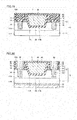
- MOSFET 1 includes a substrate 10 made of silicon carbide and having a main surface 10A, a gate insulating film 20, a gate electrode 30, an interlayer insulating film 40, a source electrode 50, a source pad electrode 60, a drain electrode 70, and a drain pad electrode 80.
- Substrate 10 includes a base substrate 11 and a semiconductor layer 12. In semiconductor layer 12, a drift region 13, a body region 14, a source region 15, and a deep region 16 are formed.
- Substrate 10 has a first trench 17 formed therein, first trench 17 opening on a main surface 10A side and having wall surfaces 17A and a bottom surface 17B.
- Base substrate 11 is made of silicon carbide, contains an n type impurity such as N (nitrogen), and therefore has n type conductivity (a first conductivity type).
- Drift region 13 is formed on a main surface 11A of base substrate 11. As with base substrate 11, drift region 13 contains an n type impurity such as N (nitrogen), and therefore has n type conductivity. The concentration thereof in drift region 13 is lower than that in base substrate 11.
- Body region 14 is formed on drift region 13 (on a side opposite to a base substrate 11 side).
- Body region 14 contains a p type impurity such as Al (aluminum) or B (boron), and therefore has p type conductivity (a second conductivity type).
- Source region 15 is formed on body region 14 (on a side opposite to a drift region 13 side).
- Source region 15 contains an n type impurity such as P (phosphorus), and therefore has n type conductivity as with base substrate 11 and drift region 13. Further, the concentration of the n type impurity contained in source region 15 is higher than that in drift region 13.
- Deep region 16 is formed to make contact with source region 15, body region 14, and drift region 13 and extend to a region deeper than first trench 17 within semiconductor layer 12. Specifically, deep region 16 is formed to make contact with source electrode 50 and penetrate source region 15 and body region 14, and such that a contact surface 16B thereof with drift region 13 is located closer to drain electrode 70 than bottom surface 17B of first trench 17. As with body region 14, deep region 16 contains a p type impurity such as Al (aluminum), and therefore has p type conductivity. The concentration thereof in deep region 16 is higher than that in body region 14.
- First trench 17 is formed to penetrate source region 15 and body region 14 and reach drift region 13. Specifically, first trench 17 is formed such that bottom surface 17B is located closer to source electrode 50 than contact surface 16B between deep region 16 and drift region 13. Further, first trench 17 is formed such that a distance between wall surface 17A and deep region 16 increases with increasing distance from main surface 10A of substrate 10. For example, first trench 17 is formed such that wall surface 17A forms an obtuse angle relative to main surface 10A of substrate 10 as shown in Fig. 1 .
- substrate 10 includes n type source region 15 including main surface 10A of substrate 10 and wall surface 17A of first trench 17, p type body region 14 making contact with source region 15 and including wall surface 17A of first trench 17, n type drift region 13 making contact with body region 14 and including wall surface 17A and bottom surface 17B of first trench 17, and p type deep region 16 making contact with body region 14 and extending to the region deeper than first trench 17.
- Gate insulating film 20 is made of, for example, SiO 2 (silicon dioxide), and is disposed on and in contact with wall surfaces 17A and bottom surface 17B of first trench 17 and main surface 10A of substrate 10.
- Gate electrode 30 is made of, for example, a conductor such as polysilicon having an impurity added therein. Gate electrode 30 is disposed on and in contact with gate insulating film 20 so as to fill first trench 17.
- Interlayer insulating film 40 is made of, for example, SiO 2 (silicon dioxide), and is disposed on and in contact with gate insulating film 20 and gate electrode 30. Specifically, interlayer insulating film 40 is disposed such that interlayer insulating film 40 and gate insulating film 20 surround gate electrode 30, thus electrically insulating gate electrode 30 from source electrode 50.
- SiO 2 silicon dioxide
- Source electrode 50 is disposed on main surface 10A of substrate 10 in contact with source region 15 and deep region 16.
- source electrode 50 is made of a material capable of making ohmic contact with source region 15, for example, Ni x Si y (nickel silicide), Ti x Si y (titanium silicide), Al x Si y (aluminum silicide), or Ti x Al y Si z (titanium aluminum silicide).
- Source electrode 50 is electrically connected to source region 15.
- Drain electrode 70 is formed on and in contact with a main surface 11 B of base substrate 11 opposite to main surface 11A thereof. Drain electrode 70 is made of, for example, the same material as that for source electrode 50, and is electrically connected to base substrate 11.
- Source pad electrode 60 is disposed on and in contact with interlayer insulating film 40 and source electrode 50.
- source pad electrode 60 is made of, for example, a conductor such as Al (aluminum), and is electrically connected to source region 15 via source electrode 50.
- Drain pad electrode 80 is disposed on and in contact with drain electrode 70.
- drain pad electrode 80 is made of, for example, a conductor such as Al (aluminum), and is electrically connected to base substrate 11 via drain electrode 70.
- MOSFET 1 serving as the semiconductor device in accordance with the present embodiment.
- a voltage applied to gate electrode 30 is less than a threshold voltage, i.e., in an OFF state, even if a voltage is applied to between source electrode 50 and drain electrode 70, a pn junction formed between body region 14 and drift region 13 is reverse-biased. Accordingly, MOSFET 1 is in an non-conductive state.
- gate electrode 30 is fed with a voltage equal to or greater than the threshold voltage, carriers are accumulated along wall surface 17A of first trench 17 in body region 14, thereby forming an inversion layer.
- source region 15 and drift region 13 are electrically connected to each other, whereby a current flows between source electrode 50 and drain electrode 70. In the manner described above, MOSFET 1 operates.
- MOSFET 1 serving as the semiconductor device in accordance with the present embodiment, p type deep region 16 extending to the region deeper than first trench 17 is formed within semiconductor layer 12 of substrate 10. Hence, electric field concentration on gate insulating film 20 can be suppressed by a depletion layer extending from a pn junction between deep region 16 and n type drift region 13. Further, in MOSFET 1, first trench 17 is formed such that the distance from deep region 16 increases with increasing distance from main surface 10A of substrate 10. Specifically, in MOSFET 1, first trench 17 is formed such that a region A sandwiched between wall surface 17A of first trench 17 and deep region 16 becomes wider from a source electrode 50 side toward a drain electrode 70 side.
- MOSFET 1 ON resistance of MOSFET 1 can be further reduced by securing wider region A as a region through which carriers pass within substrate 10.
- MOSFET 1 serving as the semiconductor device in accordance with the present embodiment is a semiconductor device having improved breakdown voltage characteristics and reduced ON resistance.
- a plane constituting main surface 10A of substrate 10 may be a plane having an off angle of 8° or smaller relative to a ⁇ 0001 ⁇ plane.
- Silicon carbide can be readily grown in a ⁇ 0001> direction. Hence, when the plane constituting main surface 10A of substrate 10 is adapted to have an off angle falling within the above-described range relative to the ⁇ 0001 ⁇ plane, substrate 10 made of silicon carbide can be prepared more readily.
- a plane constituting wall surface 17A of first trench 17 may be a plane having an off angle of not less than 50° and not more than 65° relative to the ⁇ 0001 ⁇ plane. Thereby, channel mobility in MOSFET 1 can be further improved.
- MOSFET 1 serving as the semiconductor device in accordance with the present embodiment can be manufactured.
- a substrate preparing step is performed as step (S10).
- steps (S11) and (S 12) described below are performed to prepare substrate 10 made of silicon carbide.
- step (S11) a base substrate preparing step is performed.
- an ingot (not shown) made of, for example, 4H-SiC is sliced to prepare base substrate 11 made of silicon carbide as shown in Fig. 3 .
- step (S12) an epitaxial growth layer forming step is performed.
- semiconductor layer 12 is formed by epitaxial growth on main surface 11 A of base substrate 11.
- substrate 10 including base substrate 11 and semiconductor layer 12 and having main surface 10A.
- step (S20) an active region forming step is performed.
- steps (S21) and (S22) described below are performed to form an active region in substrate 10.
- step (S21) an ion implantation step is performed.
- Al (aluminum) ions are first implanted into semiconductor layer 12, thereby forming p type body region 14.
- P (phosphorus) ions are implanted into semiconductor layer 12 to a depth shallower than the depth to which the Al ions have been implanted, thereby forming source region 15 of n type conductivity.
- Al (aluminum) ions are implanted into semiconductor layer 12 to a depth deeper than the depth to which the Al ions have been implanted, thereby forming deep region 16 of p type conductivity.
- n type source region 15 including main surface 10A of substrate 10, p type body region 14 making contact with source region 15, n type drift region 13 making contact with body region 14, and p type deep region 16 making contact with source region 15, body region 14, and drift region 13 are formed as shown in Fig. 4 .
- step (S22) an activation annealing step is performed.
- this step (S22) by heating substrate 10, the impurities implanted in step (S21) are activated. Thereby, desired carriers are generated in the regions having the impurities introduced therein, and the active region is formed in substrate 10.
- step (S30) a first trench forming step is performed.
- first trench 17 opening on the main surface 10A side is formed in substrate 10.
- a P-CVD (Plasma-Chemical Vapor Deposition) method is employed to form a mask 90 having an opening in conformity with a region of main surface 10A of substrate 10 in which first trench 17 is to be formed.
- Mask 90 is made of SiO 2 (silicon dioxide).
- substrate 10 is etched by means of Inductive Coupled Plasma Reactive Ion Etching (ICP-RIE) or the like.
- ICP-RIE Inductive Coupled Plasma Reactive Ion Etching
- thermal etching is performed in an atmosphere containing for example oxygen and a halogen-based gas such as chlorine.
- mask 90 is removed. In this way, first trench 17 having wall surface 17A at which source region 15, body region 14, and drift region 13 are exposed and bottom surface 17B is formed in substrate 10.
- deep region 16 and first trench 17 are formed such that deep region 16 is deeper than first trench 17, specifically such that contact surface 16B between deep region 16 and drift region 13 is located closer to drain electrode 70 (see Fig. 1 ) than bottom surface 17B of first trench 17. Furthermore, deep region 16 and first trench 17 are formed such that the distance between wall surface 17A of first trench 17 and deep region 16 increases with increasing distance from main surface 10A of substrate 10. Specifically, first trench 17 is formed such that wall surface 17A forms an obtuse angle relative to main surface 10A of substrate 10 as shown in Fig. 6 .
- step (S40) a gate insulating film forming step is performed.
- step (S40) by heating substrate 10 in an atmosphere containing for example oxygen, gate insulating film 20 made of SiO 2 (silicon dioxide) is disposed on and in contact with main surface 10A of substrate 10 and wall surfaces 17A and bottom surface 17B of first trench 17.
- SiO 2 silicon dioxide
- step (S50) a gate electrode forming step is performed.
- this step (S50) referring to Fig. 8 , for example, an LP (Low Pressure) CVD method is employed to form a polysilicon film having an impurity added therein, so as to fill first trench 17.
- LP Low Pressure
- step (S60) an interlayer insulating film forming step is performed.
- the CVD method is employed to form interlayer insulating film 40 made of SiO 2 (silicon dioxide) such that interlayer insulating film 40 and gate insulating film 20 surround gate electrode 30.
- step (S70) an ohmic electrode forming step is performed.
- step (S70) referring to Fig. 9 , first, interlayer insulating film 40 and gate insulating film 20 are removed from a region in which source electrode 50 is to be formed, thereby forming a region in which source region 15 and deep region 16 are exposed. Then, in this region, a metal film made of, for example, Ni is formed. Likewise, a metal film made of Ni is formed on main surface 11B of base substrate 11 opposite to main surface 11 A thereof. Then, by heating the metal films, at least portions of the metal films are silicided, thereby forming source electrode 50 and drain electrode 70 electrically connected to substrate 10.
- a pad electrode forming step is performed.
- a deposition method is employed to form source pad electrode 60, which is made of a conductor such as Al (aluminum), so as to cover source electrode 50 and interlayer insulating film 40.
- the deposition method is employed to form, on drain electrode 70, drain pad electrode 80 made of a conductor such as Al (aluminum).
- MOSFET 2 As another embodiment of the present invention will be described.
- MOSFET 2 basically has the same structure, operates in the same manner, and exhibits the same effect as those of MOSFET 1 in Embodiment 1.
- MOSFET 2 is different from MOSFET 1 in that, as shown in Fig. 10 , a second trench 18 different from first trench 17 is formed in substrate 10, and source electrode 50 serving as a contact electrode is disposed on and in contact with wall surfaces 18A and a bottom surface 18B of second trench 18.
- second trench 18 opens on the main surface 10A side, and has wall surfaces 18A and bottom surface 18B. Specifically, second trench 18 is formed to penetrate source region 15 and reach body region 14, that is, to be shallower than first trench 17.
- Source electrode 50 is disposed on and in contact with wall surfaces 18A and bottom surface 18B of second trench 18. Specifically, as in Embodiment 1, source electrode 50 is made of a material capable of making ohmic contact with source region 15, and disposed in contact with source region 15, body region 14, and deep region 16.
- MOSFET 2 serving as the semiconductor device in accordance with the present embodiment
- source electrode 50 is disposed on and in contact with wall surfaces 18A and bottom surface 18B of second trench 18 which penetrates source region 15 and reaches body region 14.
- source electrode 50 makes direct contact with body region 14 without deep region 16 interposed therebetween.
- carriers can be injected from source electrode 50 to body region 14 without influence of a depletion layer extending from a pn junction between source region 15 and deep region 16.
- MOSFET 2 serving as the semiconductor device in accordance with the present embodiment is a semiconductor device having an improved response speed.
- second trench 18 shallower than a contact surface 14A between body region 14 and drift region 13 may be formed in substrate 10 as shown in Fig. 10 .
- second trench 18 not penetrating body region 14 more specifically, second trench 18 having bottom surface 18B located closer to source electrode 50 than contact surface 14A, may be formed in substrate 10.
- second trench 18 is formed to penetrate body region 14
- body region 14 becomes thin in a region in the vicinity of wall surfaces 18A and bottom surface 18B, and as a result, punch-through is likely to occur in the region.
- second trench 18 without penetrating body region 14 as described above, occurrence of punch-through in body region 14 is avoided more readily.
- source electrode 50 may be disposed to be on and in contact with wall surfaces 18A and bottom surface 18B of second trench 18 and not to be on and in contact with main surface 10A of substrate 10, as shown in Fig. 10 .
- a distance between source electrode 50 and gate electrode 30 becomes larger than that in a case where source electrode 50 is disposed on and in contact with main surface 10A of substrate 10.
- MOSFET 2 is miniaturized, short circuit between source electrode 50 and gate electrode 30 is readily avoided.
- a plane constituting wall surface 18A of second trench 18 may be a plane crossing the ⁇ 0001 ⁇ plane.
- Substrate 10 made of silicon carbide has a characteristic that a metal is likely to be diffused in a direction parallel to the ⁇ 0001 ⁇ plane. Accordingly, when wall surface 18A of second trench 18 in contact with source electrode 50 is adapted to correspond to the plane crossing the ⁇ 0001 ⁇ plane, the metal composing source electrode 50 is facilitated to be diffused into substrate 10, thereby further reducing contact resistance between source electrode 50 and substrate 10.
- a fictitious straight line A-A extending from wall surface 18A at a lowermost portion of second trench 18 in parallel with the ⁇ 0001 ⁇ plane may cross wall surface 17A of first trench 17 facing second trench 18.
- straight line A-A may cross wall surface 17A of first trench 17 facing second trench 18, without crossing drift region 13.
- the metal composing source electrode 50 can be more effectively suppressed from being diffused into drift region 13, in particular, into drift region 13 below bottom surface 17B of first trench 17. As a result, deterioration in breakdown voltage characteristics of MOSFET 2 can be suppressed.
- a substrate preparing step is performed as step (S10).
- a base substrate preparing step (S11) and an epitaxial growth layer forming step (S 12) are performed to prepare substrate 10 made of silicon carbide and including base substrate 11 and semiconductor layer 12.
- step (S20) an active region forming step is performed.
- steps (S21) to (S23) described below are performed to form an active region in substrate 10. It should be noted that, as shown in Fig. 11 , steps (S22) and (S23) are performed after completion of steps (S30) and (S40).
- step (S21) a source/body region forming step is performed.
- Al (aluminum) ions are first implanted into semiconductor layer 12, thereby forming p type body region 14.
- P (phosphorus) ions are implanted into semiconductor layer 12 to a depth shallower than the depth to which the Al ions have been implanted, thereby forming n type source region 15.
- step (S30) a first trench forming step is performed.
- step (S30) referring to Figs. 14 and 15 , first trench 17 opening on the main surface 10A side and having wall surfaces 17A and bottom surface 17B is formed in substrate 10, as in Embodiment 1.
- step (S40) a second trench forming step is performed.
- substrate 10 is etched by means of, for example, ICP-RIE, thereby forming second trench 18 opening on the main surface 10A side and having wall surfaces 18A and bottom surface 18B.
- step (S22) a deep region forming step is performed.
- Al (aluminum) ions are implanted into a region including bottom surface 18B of second trench 18 within semiconductor layer 12, thereby forming p type deep region 16 extending to the region deeper than first trench 17.
- step (S23) an activation annealing step is performed.
- this step (S23) as in Embodiment 1, by heating substrate 10, the impurities implanted in steps (S21) and (S22) are activated, and desired carriers are generated in the regions having the impurities introduced therein.
- step (S50) a gate insulating film forming step is performed.
- this step (S50) referring to Fig. 17 , as in Embodiment 1, by heating substrate 10 in an atmosphere containing for example oxygen, gate insulating film 20 made of SiO 2 (silicon dioxide) is formed on and in contact with main surface 10A of substrate 10, wall surfaces 17A and bottom surface 17B of first trench 17, and wall surfaces 18A and bottom surface 18B of second trench 18.
- SiO 2 silicon dioxide
- step (S60) a gate electrode forming step is performed.
- this step (S60) referring to Fig. 18 , as in Embodiment 1, gate electrode 30 on and in contact with gate insulating film 20 is formed.
- step (S70) an interlayer insulating film forming step is performed.
- step (S70) referring to Fig. 19 , as in Embodiment 1, interlayer insulating film 40 is formed such that interlayer insulating film 40 and gate insulating film 20 surround gate electrode 30.
- step (S80) an ohmic electrode forming step is performed.
- step (S80) referring to Fig. 20 , first, interlayer insulating film 40 and gate insulating film 20 are removed from a region in which source electrode 50 is to be formed, thereby forming a region in which source region 15, body region 14, and deep region 16 are exposed. Then, in this region, a metal film made of, for example, Ni is formed. Likewise, a metal film made of Ni is formed on main surface 11B of base substrate 11 opposite to main surface 11 A thereof. Then, by heating the metal films, at least portions of the metal films are silicided, thereby forming source electrode 50 and drain electrode 70 electrically connected to substrate 10.
- step (S90) a pad electrode forming step is performed.
- step (S90) referring to Fig. 10 , as in Embodiment 1, source pad electrode 60 which covers source electrode 50 and interlayer insulating film 40, and drain pad electrode 80 which covers drain electrode 70 are formed.
- steps (S10) to (S90) described above MOSFET 2 is manufactured, thus completing the method for manufacturing the semiconductor device in accordance with the present embodiment.
- the semiconductor device and the method for manufacturing the semiconductor device in accordance with the present invention are particularly advantageously applicable to a semiconductor device which is required to have improved breakdown voltage characteristics and reduced ON resistance, as well as a method for manufacturing such a semiconductor device.
Landscapes
- Electrodes Of Semiconductors (AREA)
Abstract
Description
- The present invention relates to a semiconductor device and a method for manufacturing the same, and more particularly to a semiconductor device having improved breakdown voltage characteristics and reduced ON resistance, as well as a method for manufacturing such a semiconductor device.
- In recent years, in order to achieve a high breakdown voltage, low loss, and the like of semiconductor devices, silicon carbide has been adopted as a material for semiconductor devices. Silicon carbide is a wide band gap semiconductor having a band gap larger than that of silicon, which has been conventionally widely used as a material for semiconductor devices. Hence, by adopting silicon carbide as a material for a semiconductor device, the semiconductor device can have a high breakdown voltage, reduced ON resistance, and the like.
- An exemplary semiconductor device adopting silicon carbide as its material is a MOSFET (Metal Oxide Semiconductor Field Effect Transistor) or the like. The MOSFET is a semiconductor device that controls existence/non-existence of an inversion layer in a channel region in accordance with a predetermined threshold voltage so as to conduct and interrupt a current. For example, a trench gate type MOSFET or the like characterized by formation of a channel region along a wall surface of a trench has been considered.
- In the trench gate type MOSFET, ON resistance can be reduced, but breakdown voltage characteristics are disadvantageously deteriorated due to electric field concentration on a gate insulating film formed in a bottom portion of the trench. To address this, for example, it has been proposed to form in a substrate a p type deep region extending to a region as deep as or deeper than the trench, extend a depletion layer from a pn junction between the p type deep region and an n type drift region, and thereby mitigate electric field concentration on the bottom portion of the trench (see for example Japanese Patent Laying-Open No.
2009-117593 - PTL 1: Japanese Patent Laying-Open No.
2009-117593 - In the MOSFET proposed in
Patent Literature 1, the trench and the deep region are each formed to extend in a thickness direction of the substrate in parallel. Therefore, when the MOSFET is miniaturized, a region between the trench and the deep region is narrowed and thus a passage for carriers is narrowed, resulting in an increase in ON resistance of the MOSFET. - The present invention has been made in view of the foregoing problem, and one object of the present invention is to provide a semiconductor device having improved breakdown voltage characteristics and reduced ON resistance, as well as a method for manufacturing such a semiconductor device.
- A semiconductor device in accordance with the present invention includes: a substrate made of silicon carbide and having a first trench formed therein, the first trench opening on a side of one main surface; a gate insulating film disposed on and in contact with a wall surface of the first trench; and a gate electrode disposed on and in contact with the gate insulating film. The substrate includes a source region of a first conductivity type including the main surface of the substrate and the wall surface of the first trench, a body region of a second conductivity type making contact with the source region and including the wall surface of the first trench, a drift region of the first conductivity type making contact with the body region and including the wall surface of the first trench, and a deep region of the second conductivity type making contact with the body region and extending to a region deeper than the first trench. The first trench is formed such that a distance between the wall surface and the deep region increases with increasing distance from the main surface of the substrate.
- In the semiconductor device in accordance with the present invention, the deep region of the second conductivity type extending to the region deeper than the first trench is formed in the substrate. Hence, electric field concentration on the gate insulating film can be suppressed by a depletion layer extending from a pn junction between the deep region and the drift region of the first conductivity type. Further, in the semiconductor device in accordance with the present invention, the first trench is formed such that the distance from the deep region increases with increasing distance from the main surface of the substrate. This can secure a wider region through which carriers pass within the substrate, resulting in a further reduction in ON resistance of the semiconductor device. Thus, according to the semiconductor device in accordance with the present invention, there can be provided a semiconductor device having improved breakdown voltage characteristics and reduced ON resistance.
- In the semiconductor device, the wall surface of the first trench may form an obtuse angle relative to the main surface of the substrate. Thereby, the wider region through which carriers pass within the substrate is secured more readily.
- In the semiconductor device, the substrate may have a second trench formed therein, the second trench penetrating the source region and reaching the body region, opening on the side of the main surface, and being shallower than the first trench. In addition, the semiconductor device may further comprise a contact electrode disposed on and in contact with a wall surface of the second trench. This facilitates injection of carriers from the contact electrode to the body region, resulting in an improved response speed of the semiconductor device.
- In the semiconductor device, the substrate may have the second trench formed therein, the second trench being shallower than a contact surface between the body region and the drift region. Thereby, occurrence of punch-through in the body region is avoided more readily.
- In the semiconductor device, the contact electrode may be disposed not to be on and in contact with the main surface of the substrate. Thereby, short circuit between the contact electrode and the gate electrode is readily avoided.
- In the semiconductor device, a plane constituting the wall surface of the second trench may be a plane crossing a {0001} plane. Thereby, a metal composing the contact electrode is facilitated to be diffused into the substrate, and as a result, contact resistance between the contact electrode and the substrate can be further reduced.
- In the semiconductor device, in a cross section along a thickness direction of the substrate including the first and second trenches, a fictitious straight line extending from the wall surface at a lowermost portion of the second trench in parallel with a {0001} plane may cross the wall surface of the first trench facing the second trench. Thereby, deterioration in breakdown voltage characteristics of the semiconductor device can be suppressed.
- In the semiconductor device, in the cross section along the thickness direction of the substrate including the first and second trenches, the fictitious straight line may cross the wall surface of the first trench facing the second trench, without crossing the drift region. Thereby, the deterioration in breakdown voltage characteristics of the semiconductor device can be suppressed more effectively.
- In the semiconductor device, a plane constituting the main surface of the substrate may be a plane having an off angle of 8° or smaller relative to a {0001} plane. Thereby, a substrate made of silicon carbide can be prepared more readily.
- In the semiconductor device, a plane constituting the wall surface of the first trench may be a plane having an off angle of not less than 50° and not more than 65° relative to a {0001} plane. Thereby, channel mobility in the semiconductor device can be further improved.
- A method for manufacturing a semiconductor device in accordance with the present invention includes the steps of: preparing a substrate made of silicon carbide and having a main surface; forming an active region in the substrate; forming a first trench opening on a side of the main surface of the substrate; disposing a gate insulating film on and in contact with a wall surface of the first trench; and disposing a gate electrode on and in contact with the gate insulating film. In the step of forming the active region, a source region of a first conductivity type, a body region of a second conductivity type, a drift region of the first conductivity type, and a deep region of the second conductivity type are formed, the source region including the main surface of the substrate, the body region making contact with the source region, the drift region making contact with the body region, and the deep region making contact with the body region. In the step of forming the first trench, the first trench is formed to have the wall surface at which the source region, the body region, and the drift region are exposed. The deep region and the first trench are formed such that the deep region is deeper than the first trench and a distance between the wall surface of the first trench and the deep region increases with increasing distance from the main surface of the substrate.
- According to the method for manufacturing the semiconductor device in accordance with the present invention, there can be manufactured a semiconductor device in accordance with the present invention having improved breakdown voltage characteristics and reduced ON resistance.
- As apparent from the description above, according to the semiconductor device and the method for manufacturing the same in accordance with the present invention, there can be provided a semiconductor device having improved breakdown voltage characteristics and reduced ON resistance, as well as a method for manufacturing such a semiconductor device.
-
-
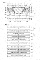
Fig. 1 is a schematic cross sectional view showing a structure of a MOSFET. -
Fig. 2 is a flowchart schematically showing a method for manufacturing the MOSFET. -
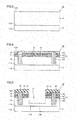
Fig. 3 is a schematic cross sectional view for illustrating the method for manufacturing the MOSFET. -
Fig. 4 is a schematic cross sectional view for illustrating the method for manufacturing the MOSFET. -
Fig. 5 is a schematic cross sectional view for illustrating the method for manufacturing the MOSFET. -
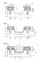
Fig. 6 is a schematic cross sectional view for illustrating the method for manufacturing the MOSFET. -
Fig. 7 is a schematic cross sectional view for illustrating the method for manufacturing the MOSFET. -
Fig. 8 is a schematic cross sectional view for illustrating the method for manufacturing the MOSFET. -
Fig. 9 is a schematic cross sectional view for illustrating the method for manufacturing the MOSFET. -
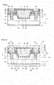
Fig. 10 is a schematic cross sectional view showing a structure of a MOSFET in accordance withEmbodiment 2. -
Fig. 11 is a flowchart schematically showing a method for manufacturing the MOSFET in accordance withEmbodiment 2. -
Fig. 12 is a schematic cross sectional view for illustrating the method for manufacturing the MOSFET in accordance withEmbodiment 2. -
Fig. 13 is a schematic cross sectional view for illustrating the method for manufacturing the MOSFET in accordance withEmbodiment 2. -
Fig. 14 is a schematic cross sectional view for illustrating the method for manufacturing the MOSFET in accordance withEmbodiment 2. -
Fig. 15 is a schematic cross sectional view for illustrating the method for manufacturing the MOSFET in accordance withEmbodiment 2. -
Fig. 16 is a schematic cross sectional view for illustrating the method for manufacturing the MOSFET in accordance withEmbodiment 2. -
Fig. 17 is a schematic cross sectional view for illustrating the method for manufacturing the MOSFET in accordance withEmbodiment 2. -
Fig. 18 is a schematic cross sectional view for illustrating the method for manufacturing the MOSFET in accordance withEmbodiment 2. -
Fig. 19 is a schematic cross sectional view for illustrating the method for manufacturing the MOSFET in accordance withEmbodiment 2. -
Fig. 20 is a schematic cross sectional view for illustrating the method for manufacturing the MOSFET in accordance withEmbodiment 2. - The hollowing describes embodiments of the present invention with reference to the drawings. It should be noted that in the below-described drawings, the same or corresponding portions are given the same reference characters and are not described repeatedly. Further, in the present specification, an individual orientation is represented by [], a group orientation is represented by o, an individual plane is represented by 0, and a group plane is represented by { }. In addition, a negative index is supposed to be crystallographically indicated by putting "-" (bar) above a numeral, but is indicated by putting the negative sign before the numeral in the present specification.
-
Embodiment 1 as one embodiment of the present invention will now be described. First, a structure of aMOSFET 1 serving as a semiconductor device in accordance with the present embodiment will be described. Referring toFig. 1 ,MOSFET 1 includes asubstrate 10 made of silicon carbide and having amain surface 10A, agate insulating film 20, agate electrode 30, aninterlayer insulating film 40, asource electrode 50, asource pad electrode 60, adrain electrode 70, and adrain pad electrode 80.Substrate 10 includes abase substrate 11 and asemiconductor layer 12. Insemiconductor layer 12, adrift region 13, abody region 14, asource region 15, and adeep region 16 are formed.Substrate 10 has afirst trench 17 formed therein,first trench 17 opening on amain surface 10A side and havingwall surfaces 17A and abottom surface 17B. -
Base substrate 11 is made of silicon carbide, contains an n type impurity such as N (nitrogen), and therefore has n type conductivity (a first conductivity type).Drift region 13 is formed on amain surface 11A ofbase substrate 11. As withbase substrate 11, driftregion 13 contains an n type impurity such as N (nitrogen), and therefore has n type conductivity. The concentration thereof indrift region 13 is lower than that inbase substrate 11. -
Body region 14 is formed on drift region 13 (on a side opposite to abase substrate 11 side).Body region 14 contains a p type impurity such as Al (aluminum) or B (boron), and therefore has p type conductivity (a second conductivity type). -
Source region 15 is formed on body region 14 (on a side opposite to adrift region 13 side).Source region 15 contains an n type impurity such as P (phosphorus), and therefore has n type conductivity as withbase substrate 11 and driftregion 13. Further, the concentration of the n type impurity contained insource region 15 is higher than that indrift region 13. -
Deep region 16 is formed to make contact withsource region 15,body region 14, and driftregion 13 and extend to a region deeper thanfirst trench 17 withinsemiconductor layer 12. Specifically,deep region 16 is formed to make contact withsource electrode 50 and penetratesource region 15 andbody region 14, and such that acontact surface 16B thereof withdrift region 13 is located closer to drainelectrode 70 thanbottom surface 17B offirst trench 17. As withbody region 14,deep region 16 contains a p type impurity such as Al (aluminum), and therefore has p type conductivity. The concentration thereof indeep region 16 is higher than that inbody region 14. -
First trench 17 is formed to penetratesource region 15 andbody region 14 and reachdrift region 13. Specifically,first trench 17 is formed such thatbottom surface 17B is located closer to sourceelectrode 50 thancontact surface 16B betweendeep region 16 and driftregion 13. Further,first trench 17 is formed such that a distance betweenwall surface 17A anddeep region 16 increases with increasing distance frommain surface 10A ofsubstrate 10. For example,first trench 17 is formed such that wall surface 17A forms an obtuse angle relative tomain surface 10A ofsubstrate 10 as shown inFig. 1 . - Thus,
substrate 10 includes ntype source region 15 includingmain surface 10A ofsubstrate 10 andwall surface 17A offirst trench 17, ptype body region 14 making contact withsource region 15 and includingwall surface 17A offirst trench 17, ntype drift region 13 making contact withbody region 14 and includingwall surface 17A andbottom surface 17B offirst trench 17, and p typedeep region 16 making contact withbody region 14 and extending to the region deeper thanfirst trench 17. -
Gate insulating film 20 is made of, for example, SiO2 (silicon dioxide), and is disposed on and in contact withwall surfaces 17A andbottom surface 17B offirst trench 17 andmain surface 10A ofsubstrate 10. -
Gate electrode 30 is made of, for example, a conductor such as polysilicon having an impurity added therein.Gate electrode 30 is disposed on and in contact withgate insulating film 20 so as to fillfirst trench 17. -
Interlayer insulating film 40 is made of, for example, SiO2 (silicon dioxide), and is disposed on and in contact withgate insulating film 20 andgate electrode 30. Specifically,interlayer insulating film 40 is disposed such thatinterlayer insulating film 40 andgate insulating film 20surround gate electrode 30, thus electrically insulatinggate electrode 30 fromsource electrode 50. -
Source electrode 50 is disposed onmain surface 10A ofsubstrate 10 in contact withsource region 15 anddeep region 16. Specifically,source electrode 50 is made of a material capable of making ohmic contact withsource region 15, for example, NixSiy (nickel silicide), TixSiy (titanium silicide), AlxSiy (aluminum silicide), or TixAlySiz (titanium aluminum silicide).Source electrode 50 is electrically connected to sourceregion 15. -
Drain electrode 70 is formed on and in contact with amain surface 11 B ofbase substrate 11 opposite tomain surface 11A thereof.Drain electrode 70 is made of, for example, the same material as that forsource electrode 50, and is electrically connected tobase substrate 11. -
Source pad electrode 60 is disposed on and in contact with interlayer insulatingfilm 40 andsource electrode 50. Specifically,source pad electrode 60 is made of, for example, a conductor such as Al (aluminum), and is electrically connected to sourceregion 15 viasource electrode 50. -
Drain pad electrode 80 is disposed on and in contact withdrain electrode 70. Specifically, as withsource pad electrode 60,drain pad electrode 80 is made of, for example, a conductor such as Al (aluminum), and is electrically connected tobase substrate 11 viadrain electrode 70. - Next, an operation of
MOSFET 1 serving as the semiconductor device in accordance with the present embodiment will be described. Referring toFig. 1 , in a state where a voltage applied togate electrode 30 is less than a threshold voltage, i.e., in an OFF state, even if a voltage is applied to betweensource electrode 50 anddrain electrode 70, a pn junction formed betweenbody region 14 and driftregion 13 is reverse-biased. Accordingly,MOSFET 1 is in an non-conductive state. On the other hand, whengate electrode 30 is fed with a voltage equal to or greater than the threshold voltage, carriers are accumulated alongwall surface 17A offirst trench 17 inbody region 14, thereby forming an inversion layer. As a result,source region 15 and driftregion 13 are electrically connected to each other, whereby a current flows betweensource electrode 50 anddrain electrode 70. In the manner described above,MOSFET 1 operates. - As described above, in
MOSFET 1 serving as the semiconductor device in accordance with the present embodiment, p typedeep region 16 extending to the region deeper thanfirst trench 17 is formed withinsemiconductor layer 12 ofsubstrate 10. Hence, electric field concentration ongate insulating film 20 can be suppressed by a depletion layer extending from a pn junction betweendeep region 16 and ntype drift region 13. Further, inMOSFET 1,first trench 17 is formed such that the distance fromdeep region 16 increases with increasing distance frommain surface 10A ofsubstrate 10. Specifically, inMOSFET 1,first trench 17 is formed such that a region A sandwiched betweenwall surface 17A offirst trench 17 anddeep region 16 becomes wider from asource electrode 50 side toward adrain electrode 70 side. Accordingly, inMOSFET 1, ON resistance ofMOSFET 1 can be further reduced by securing wider region A as a region through which carriers pass withinsubstrate 10. Thus,MOSFET 1 serving as the semiconductor device in accordance with the present embodiment is a semiconductor device having improved breakdown voltage characteristics and reduced ON resistance. - Further, in
MOSFET 1, a plane constitutingmain surface 10A ofsubstrate 10 may be a plane having an off angle of 8° or smaller relative to a {0001} plane. - Silicon carbide can be readily grown in a <0001> direction. Hence, when the plane constituting
main surface 10A ofsubstrate 10 is adapted to have an off angle falling within the above-described range relative to the {0001} plane,substrate 10 made of silicon carbide can be prepared more readily. - Further, in
MOSFET 1, a plane constitutingwall surface 17A offirst trench 17 may be a plane having an off angle of not less than 50° and not more than 65° relative to the {0001} plane. Thereby, channel mobility inMOSFET 1 can be further improved. - Next, a method for manufacturing the semiconductor device in accordance with the present embodiment will be described with reference to
Figs. 1 to 9 . In the method for manufacturing the semiconductor device in accordance with the present embodiment,MOSFET 1 serving as the semiconductor device in accordance with the present embodiment can be manufactured. Referring toFig. 2 , first, a substrate preparing step is performed as step (S10). In this step (S10), steps (S11) and (S 12) described below are performed to preparesubstrate 10 made of silicon carbide. - First, as step (S11), a base substrate preparing step is performed. In this step (S11), an ingot (not shown) made of, for example, 4H-SiC is sliced to prepare
base substrate 11 made of silicon carbide as shown inFig. 3 . - Next, as step (S12), an epitaxial growth layer forming step is performed. In this step (S12), referring to
Fig. 3 ,semiconductor layer 12 is formed by epitaxial growth onmain surface 11 A ofbase substrate 11. In this way, there isprepared substrate 10 includingbase substrate 11 andsemiconductor layer 12 and havingmain surface 10A. - Next, as step (S20), an active region forming step is performed. In this step (S20), steps (S21) and (S22) described below are performed to form an active region in
substrate 10. - First, as step (S21), an ion implantation step is performed. In this step (S21), referring to
Fig. 4 , for example, Al (aluminum) ions are first implanted intosemiconductor layer 12, thereby forming ptype body region 14. Next, for example, P (phosphorus) ions are implanted intosemiconductor layer 12 to a depth shallower than the depth to which the Al ions have been implanted, thereby formingsource region 15 of n type conductivity. Then, for example, Al (aluminum) ions are implanted intosemiconductor layer 12 to a depth deeper than the depth to which the Al ions have been implanted, thereby formingdeep region 16 of p type conductivity. Further, insemiconductor layer 12, a region in which none ofbody region 14,source region 15, anddeep region 16 is formed serves asdrift region 13. In this way, ntype source region 15 includingmain surface 10A ofsubstrate 10, ptype body region 14 making contact withsource region 15, ntype drift region 13 making contact withbody region 14, and p typedeep region 16 making contact withsource region 15,body region 14, and driftregion 13 are formed as shown inFig. 4 . - Next, as step (S22), an activation annealing step is performed. In this step (S22), by
heating substrate 10, the impurities implanted in step (S21) are activated. Thereby, desired carriers are generated in the regions having the impurities introduced therein, and the active region is formed insubstrate 10. - Next, as step (S30), a first trench forming step is performed. In this step (S30), referring to
Figs. 5 and6 ,first trench 17 opening on themain surface 10A side is formed insubstrate 10. Specifically, referring toFig. 5 , first, for example a P-CVD (Plasma-Chemical Vapor Deposition) method is employed to form amask 90 having an opening in conformity with a region ofmain surface 10A ofsubstrate 10 in whichfirst trench 17 is to be formed.Mask 90 is made of SiO2 (silicon dioxide). Next, in an atmosphere containing for example SF6 (sulfur hexafluoride) gas and oxygen,substrate 10 is etched by means of Inductive Coupled Plasma Reactive Ion Etching (ICP-RIE) or the like. Next, referring toFig. 6 , thermal etching is performed in an atmosphere containing for example oxygen and a halogen-based gas such as chlorine. After completion of the etching,mask 90 is removed. In this way,first trench 17 havingwall surface 17A at whichsource region 15,body region 14, and driftregion 13 are exposed andbottom surface 17B is formed insubstrate 10. - Further, as shown in
Fig. 6 ,deep region 16 andfirst trench 17 are formed such thatdeep region 16 is deeper thanfirst trench 17, specifically such thatcontact surface 16B betweendeep region 16 and driftregion 13 is located closer to drain electrode 70 (seeFig. 1 ) thanbottom surface 17B offirst trench 17. Furthermore,deep region 16 andfirst trench 17 are formed such that the distance betweenwall surface 17A offirst trench 17 anddeep region 16 increases with increasing distance frommain surface 10A ofsubstrate 10. Specifically,first trench 17 is formed such that wall surface 17A forms an obtuse angle relative tomain surface 10A ofsubstrate 10 as shown inFig. 6 . - Next, as step (S40), a gate insulating film forming step is performed. In this step (S40), referring to
Fig. 7 , byheating substrate 10 in an atmosphere containing for example oxygen,gate insulating film 20 made of SiO2 (silicon dioxide) is disposed on and in contact withmain surface 10A ofsubstrate 10 andwall surfaces 17A andbottom surface 17B offirst trench 17. - Next, as step (S50), a gate electrode forming step is performed. In this step (S50), referring to
Fig. 8 , for example, an LP (Low Pressure) CVD method is employed to form a polysilicon film having an impurity added therein, so as to fillfirst trench 17. Thereby,gate electrode 30 on and in contact withgate insulating film 20 is disposed. - Next, as step (S60), an interlayer insulating film forming step is performed. In this step (S60), referring to
Fig. 9 , for example, the CVD method is employed to form interlayer insulatingfilm 40 made of SiO2 (silicon dioxide) such thatinterlayer insulating film 40 andgate insulating film 20surround gate electrode 30. - Next, as step (S70), an ohmic electrode forming step is performed. In this step (S70), referring to
Fig. 9 , first,interlayer insulating film 40 andgate insulating film 20 are removed from a region in which source electrode 50 is to be formed, thereby forming a region in whichsource region 15 anddeep region 16 are exposed. Then, in this region, a metal film made of, for example, Ni is formed. Likewise, a metal film made of Ni is formed onmain surface 11B ofbase substrate 11 opposite tomain surface 11 A thereof. Then, by heating the metal films, at least portions of the metal films are silicided, thereby formingsource electrode 50 anddrain electrode 70 electrically connected tosubstrate 10. - Next, as step (S80), a pad electrode forming step is performed. In this step (S80), referring to
Fig. 1 , for example, a deposition method is employed to formsource pad electrode 60, which is made of a conductor such as Al (aluminum), so as to coversource electrode 50 andinterlayer insulating film 40. Further, as withsource pad electrode 60, for example, the deposition method is employed to form, ondrain electrode 70,drain pad electrode 80 made of a conductor such as Al (aluminum). By performing steps (S10) to (S80) described above,MOSFET 1 is manufactured, thus completing the method for manufacturing the semiconductor device in accordance with the present embodiment. Thus, according to the method for manufacturing the semiconductor device in accordance with the present embodiment, there can be manufacturedMOSFET 1 which serves as the semiconductor device in accordance with the present embodiment having improved breakdown voltage characteristics and reduced ON resistance. - Next,
Embodiment 2 as another embodiment of the present invention will be described. First, a structure of aMOSFET 2 serving as a semiconductor device in accordance with the present embodiment will be described. Referring toFig. 10 ,MOSFET 2 basically has the same structure, operates in the same manner, and exhibits the same effect as those ofMOSFET 1 inEmbodiment 1. However,MOSFET 2 is different fromMOSFET 1 in that, as shown inFig. 10 , asecond trench 18 different fromfirst trench 17 is formed insubstrate 10, andsource electrode 50 serving as a contact electrode is disposed on and in contact withwall surfaces 18A and abottom surface 18B ofsecond trench 18. - Referring to
Fig. 10 ,second trench 18 opens on themain surface 10A side, and haswall surfaces 18A andbottom surface 18B. Specifically,second trench 18 is formed to penetratesource region 15 and reachbody region 14, that is, to be shallower thanfirst trench 17. -
Source electrode 50 is disposed on and in contact withwall surfaces 18A andbottom surface 18B ofsecond trench 18. Specifically, as inEmbodiment 1,source electrode 50 is made of a material capable of making ohmic contact withsource region 15, and disposed in contact withsource region 15,body region 14, anddeep region 16. - As described above, in
MOSFET 2 serving as the semiconductor device in accordance with the present embodiment,source electrode 50 is disposed on and in contact withwall surfaces 18A andbottom surface 18B ofsecond trench 18 which penetratessource region 15 and reachesbody region 14. Hence, unlike that inMOSFET 1,source electrode 50 makes direct contact withbody region 14 withoutdeep region 16 interposed therebetween. Accordingly, inMOSFET 2, carriers can be injected fromsource electrode 50 tobody region 14 without influence of a depletion layer extending from a pn junction betweensource region 15 anddeep region 16. As a result, the operating state ofMOSFET 2 is readily switched. Thus,MOSFET 2 serving as the semiconductor device in accordance with the present embodiment is a semiconductor device having an improved response speed. - Further, in
MOSFET 2,second trench 18 shallower than acontact surface 14A betweenbody region 14 and driftregion 13 may be formed insubstrate 10 as shown inFig. 10 . Specifically,second trench 18 not penetratingbody region 14, more specifically,second trench 18 havingbottom surface 18B located closer to sourceelectrode 50 thancontact surface 14A, may be formed insubstrate 10. Whensecond trench 18 is formed to penetratebody region 14,body region 14 becomes thin in a region in the vicinity ofwall surfaces 18A andbottom surface 18B, and as a result, punch-through is likely to occur in the region. In contrast, by formingsecond trench 18 without penetratingbody region 14 as described above, occurrence of punch-through inbody region 14 is avoided more readily. - Further, in
MOSFET 2,source electrode 50 may be disposed to be on and in contact withwall surfaces 18A andbottom surface 18B ofsecond trench 18 and not to be on and in contact withmain surface 10A ofsubstrate 10, as shown inFig. 10 . - Thereby, a distance between
source electrode 50 andgate electrode 30 becomes larger than that in a case where source electrode 50 is disposed on and in contact withmain surface 10A ofsubstrate 10. As a result, for example whenMOSFET 2 is miniaturized, short circuit betweensource electrode 50 andgate electrode 30 is readily avoided. - Further, in
MOSFET 2, a plane constitutingwall surface 18A ofsecond trench 18 may be a plane crossing the {0001} plane. -
Substrate 10 made of silicon carbide has a characteristic that a metal is likely to be diffused in a direction parallel to the {0001} plane. Accordingly, whenwall surface 18A ofsecond trench 18 in contact withsource electrode 50 is adapted to correspond to the plane crossing the {0001} plane, the metalcomposing source electrode 50 is facilitated to be diffused intosubstrate 10, thereby further reducing contact resistance betweensource electrode 50 andsubstrate 10. - Further, in
MOSFET 2, in a cross section along a thickness direction ofsubstrate 10 including first andsecond trenches wall surface 18A at a lowermost portion ofsecond trench 18 in parallel with the {0001} plane may crosswall surface 17A offirst trench 17 facingsecond trench 18. Specifically, as shown inFig. 10 , straight line A-A may crosswall surface 17A offirst trench 17 facingsecond trench 18, without crossingdrift region 13. - Thereby, the metal
composing source electrode 50 can be more effectively suppressed from being diffused intodrift region 13, in particular, intodrift region 13 belowbottom surface 17B offirst trench 17. As a result, deterioration in breakdown voltage characteristics ofMOSFET 2 can be suppressed. - Next, a method for manufacturing the semiconductor device in accordance with the present embodiment will be described. In the method for manufacturing the semiconductor device in accordance with the present embodiment,
MOSFET 2 serving as the semiconductor device in accordance with the present embodiment is manufactured. Referring toFig. 11 , first, a substrate preparing step is performed as step (S10). In this step (S10), referring toFig. 12 , as inEmbodiment 1, a base substrate preparing step (S11) and an epitaxial growth layer forming step (S 12) are performed to preparesubstrate 10 made of silicon carbide and includingbase substrate 11 andsemiconductor layer 12. - Next, as step (S20), an active region forming step is performed. In this step (S20), steps (S21) to (S23) described below are performed to form an active region in
substrate 10. It should be noted that, as shown inFig. 11 , steps (S22) and (S23) are performed after completion of steps (S30) and (S40). - First, as step (S21), a source/body region forming step is performed. In this step (S21), referring to
Fig. 13 , for example, Al (aluminum) ions are first implanted intosemiconductor layer 12, thereby forming ptype body region 14. Next, for example, P (phosphorus) ions are implanted intosemiconductor layer 12 to a depth shallower than the depth to which the Al ions have been implanted, thereby forming ntype source region 15. - Next, as step (S30), a first trench forming step is performed. In this step (S30), referring to
Figs. 14 and 15 ,first trench 17 opening on themain surface 10A side and havingwall surfaces 17A andbottom surface 17B is formed insubstrate 10, as inEmbodiment 1. - Next, as step (S40), a second trench forming step is performed. In this step (S40), referring to
Fig. 16 ,substrate 10 is etched by means of, for example, ICP-RIE, thereby formingsecond trench 18 opening on themain surface 10A side and havingwall surfaces 18A andbottom surface 18B. - Next, as step (S22), a deep region forming step is performed. In this step (S22), referring to
Fig. 16 , for example, Al (aluminum) ions are implanted into a region includingbottom surface 18B ofsecond trench 18 withinsemiconductor layer 12, thereby forming p typedeep region 16 extending to the region deeper thanfirst trench 17. - Next, as step (S23), an activation annealing step is performed. In this step (S23), as in
Embodiment 1, byheating substrate 10, the impurities implanted in steps (S21) and (S22) are activated, and desired carriers are generated in the regions having the impurities introduced therein. - Next, as step (S50), a gate insulating film forming step is performed. In this step (S50), referring to
Fig. 17 , as inEmbodiment 1, byheating substrate 10 in an atmosphere containing for example oxygen,gate insulating film 20 made of SiO2 (silicon dioxide) is formed on and in contact withmain surface 10A ofsubstrate 10, wall surfaces 17A andbottom surface 17B offirst trench 17, andwall surfaces 18A andbottom surface 18B ofsecond trench 18. - Next, as step (S60), a gate electrode forming step is performed. In this step (S60), referring to
Fig. 18 , as inEmbodiment 1,gate electrode 30 on and in contact withgate insulating film 20 is formed. - Next, as step (S70), an interlayer insulating film forming step is performed. In this step (S70), referring to
Fig. 19 , as inEmbodiment 1,interlayer insulating film 40 is formed such thatinterlayer insulating film 40 andgate insulating film 20surround gate electrode 30. - Next, as step (S80), an ohmic electrode forming step is performed. In this step (S80), referring to
Fig. 20 , first,interlayer insulating film 40 andgate insulating film 20 are removed from a region in which source electrode 50 is to be formed, thereby forming a region in whichsource region 15,body region 14, anddeep region 16 are exposed. Then, in this region, a metal film made of, for example, Ni is formed. Likewise, a metal film made of Ni is formed onmain surface 11B ofbase substrate 11 opposite tomain surface 11 A thereof. Then, by heating the metal films, at least portions of the metal films are silicided, thereby formingsource electrode 50 anddrain electrode 70 electrically connected tosubstrate 10. - Next, as step (S90), a pad electrode forming step is performed. In this step (S90), referring to
Fig. 10 , as inEmbodiment 1,source pad electrode 60 which coverssource electrode 50 andinterlayer insulating film 40, anddrain pad electrode 80 which coversdrain electrode 70 are formed. By performing steps (S10) to (S90) described above,MOSFET 2 is manufactured, thus completing the method for manufacturing the semiconductor device in accordance with the present embodiment. - It should be understood that the embodiments disclosed herein are illustrative and non-restrictive in every respect. The scope of the present invention is defined by the scope of the claims, rather than the description above, and is intended to include any modifications within the scope and meaning equivalent to the scope of the claims.
- The semiconductor device and the method for manufacturing the semiconductor device in accordance with the present invention are particularly advantageously applicable to a semiconductor device which is required to have improved breakdown voltage characteristics and reduced ON resistance, as well as a method for manufacturing such a semiconductor device.
- 1,2: MOSFET; 10: substrate; 11: base substrate; 10A, 11 A, 11B: main surface; 12: semiconductor layer; 13: drift region; 14: body region; 15: source region; 16: deep region; 14A, 16B: contact surface; 17: first trench; 18: second trench; 17A, 18A: wall surface; 17B, 18B: bottom surface; 20: gate insulating film; 30: gate electrode; 40: interlayer insulating film; 50: source electrode; 60: source pad electrode; 70: drain electrode; 80: drain pad electrode; 90: mask.
Claims (11)
- A semiconductor device (1, 2), comprising:a substrate (10) made of silicon carbide and having a first trench (17) formed therein, said first trench (17) opening on a side of one main surface (10A);a gate insulating film (20) disposed on and in contact with a wall surface (17A) of said first trench (17); anda gate electrode (30) disposed on and in contact with said gate insulating film (20),said substrate (10) including
a source region (15) of a first conductivity type including said main surface (10A) of said substrate (10) and said wall surface (17A) of said first trench (17),
a body region (14) of a second conductivity type making contact with said source region (15) and including said wall surface (17A) of said first trench (17),
a drift region (13) of the first conductivity type making contact with said body region (14) and including said wall surface (17A) of said first trench (17), and
a deep region (16) of the second conductivity type making contact with said body region (14) and extending to a region deeper than said first trench (17),said first trench (17) being formed such that a distance between said wall surface (17A) and said deep region (16) increases with increasing distance from said main surface (10A) of said substrate (10). - The semiconductor device (1, 2) according to claim 1, wherein said wall surface (17A) of said first trench (17) forms an obtuse angle relative to said main surface (10A) of said substrate (10).
- The semiconductor device (2) according to claim 1 or 2, wherein
said substrate (10) has a second trench (18) formed therein, said second trench (18) penetrating said source region (15) and reaching said body region (14), opening on the side of said main surface (10A), and being shallower than said first trench (17), and
said semiconductor device further comprises a contact electrode (50) disposed on and in contact with a wall surface (18A) of said second trench (18). - The semiconductor device (2) according to claim 3, wherein said substrate (10) has said second trench (18) formed therein, said second trench (18) being shallower than a contact surface (14A) between said body region (14) and said drift region (13).
- The semiconductor device (2) according to claim 3 or 4, wherein said contact electrode (50) is disposed not to be on and in contact with said main surface (10A) of said substrate (10).
- The semiconductor device (2) according to any of claims 3 to 5, wherein a plane constituting said wall surface (18A) of said second trench (18) is a plane crossing a {0001} plane.
- The semiconductor device (2) according to any of claims 3 to 6, wherein in a cross section along a thickness direction of said substrate (10) including said first and second trenches (17, 18), a fictitious straight line (A-A) extending from said wall surface (18A) at a lowermost portion of said second trench (18) in parallel with a {0001} plane crosses said wall surface (17A) of said first trench (17) facing said second trench (18).
- The semiconductor device (2) according to claim 7, wherein in the cross section along the thickness direction of said substrate (10) including said first and second trenches (17, 18), said fictitious straight line (A-A) crosses said wall surface (17A) of said first trench (17) facing said second trench (18), without crossing said drift region (13).
- The semiconductor device (1, 2) according to any of claims 1 to 8, wherein a plane constituting said main surface (10A) of said substrate (10) is a plane having an off angle of 8° or smaller relative to a {0001} plane.
- The semiconductor device (1, 2) according to any of claims 1 to 9, wherein a plane constituting said wall surface (17A) of said first trench (17) is a plane having an off angle of not less than 50° and not more than 65° relative to a {0001} plane.
- A method for manufacturing a semiconductor device, comprising the steps of:preparing a substrate (10) made of silicon carbide and having a main surface (10A);forming an active region in said substrate (10);forming a first trench (17) opening on a side of said main surface (10A) of said substrate (10);disposing a gate insulating film (20) on and in contact with a wall surface (17A) of said first trench (17); anddisposing a gate electrode (30) on and in contact with said gate insulating film (20),in the step of forming said active region, a source region (15) of a first conductivity type, a body region (14) of a second conductivity type, a drift region (13) of the first conductivity type, and a deep region (16) of the second conductivity type being formed, said source region (15) including said main surface (10A) of said substrate (10), said body region (14) making contact with said source region (15), said drift region (13) making contact with said body region (14), and said deep region (16) making contact with said body region (14),in the step of forming said first trench (17), said first trench (17) being formed to have the wall surface (17A) at which said source region (15), said body region (14), and said drift region (13) are exposed,said deep region (16) and said first trench (17) being formed such that said deep region (16) is deeper than said first trench (17) and a distance between said wall surface (17A) of said first trench (17) and said deep region (16) increases with increasing distance from said main surface (10A) of said substrate (10).
Applications Claiming Priority (2)
| Application Number | Priority Date | Filing Date | Title |
|---|---|---|---|
| JP2012004641A JP2013145770A (en) | 2012-01-13 | 2012-01-13 | Semiconductor device and manufacturing method of the same |
| PCT/JP2012/080822 WO2013105353A1 (en) | 2012-01-13 | 2012-11-29 | Semiconductor device and method of manufacturing thereof |
Publications (2)
| Publication Number | Publication Date |
|---|---|
| EP2804216A1 true EP2804216A1 (en) | 2014-11-19 |
| EP2804216A4 EP2804216A4 (en) | 2015-08-19 |
Family
ID=48779366
Family Applications (1)
| Application Number | Title | Priority Date | Filing Date |
|---|---|---|---|
| EP12864778.1A Withdrawn EP2804216A4 (en) | 2012-01-13 | 2012-11-29 | Semiconductor device and method of manufacturing thereof |
Country Status (6)
| Country | Link |
|---|---|
| US (1) | US9099553B2 (en) |
| EP (1) | EP2804216A4 (en) |
| JP (1) | JP2013145770A (en) |
| KR (1) | KR20140114338A (en) |
| CN (1) | CN103959476B (en) |
| WO (1) | WO2013105353A1 (en) |
Cited By (1)
| Publication number | Priority date | Publication date | Assignee | Title |
|---|---|---|---|---|
| CN112436057A (en) * | 2020-10-15 | 2021-03-02 | 上海芯导电子科技股份有限公司 | Low-on-resistance MOS device and preparation process thereof |
Families Citing this family (16)
| Publication number | Priority date | Publication date | Assignee | Title |
|---|---|---|---|---|
| JP2013131512A (en) * | 2011-12-20 | 2013-07-04 | Sumitomo Electric Ind Ltd | Semiconductor device and method of manufacturing the same |
| JP2013145770A (en) | 2012-01-13 | 2013-07-25 | Sumitomo Electric Ind Ltd | Semiconductor device and manufacturing method of the same |
| US9853140B2 (en) | 2012-12-31 | 2017-12-26 | Vishay-Siliconix | Adaptive charge balanced MOSFET techniques |
| JP6048317B2 (en) * | 2013-06-05 | 2016-12-21 | 株式会社デンソー | Silicon carbide semiconductor device |
| JP2014241368A (en) * | 2013-06-12 | 2014-12-25 | 住友電気工業株式会社 | Silicon carbide semiconductor device |
| WO2015072052A1 (en) * | 2013-11-13 | 2015-05-21 | 三菱電機株式会社 | Semiconductor device |
| JP2015099845A (en) * | 2013-11-19 | 2015-05-28 | 住友電気工業株式会社 | Semiconductor device |
| DE102014200429A1 (en) * | 2014-01-13 | 2015-07-16 | Robert Bosch Gmbh | Trench MOSFET transistor device, substrate for trench MOSFET transistor device and corresponding manufacturing method |
| JP6560059B2 (en) * | 2015-08-20 | 2019-08-14 | ルネサスエレクトロニクス株式会社 | Semiconductor device and manufacturing method thereof |
| JP6651894B2 (en) * | 2016-02-23 | 2020-02-19 | 株式会社デンソー | Compound semiconductor device and method of manufacturing the same |
| JP6708954B2 (en) * | 2016-03-31 | 2020-06-10 | 住友電気工業株式会社 | Silicon carbide semiconductor device |
| JP6587265B2 (en) | 2016-04-14 | 2019-10-09 | 住友電気工業株式会社 | Silicon carbide semiconductor device and manufacturing method thereof |
| JP6658406B2 (en) * | 2016-08-31 | 2020-03-04 | 株式会社デンソー | Method for manufacturing silicon carbide semiconductor device |
| US20190198622A1 (en) * | 2016-08-31 | 2019-06-27 | Sumitomo Electric Industries, Ltd. | Silicon carbide semiconductor device and method for manufacturing same |
| KR101875638B1 (en) * | 2016-10-14 | 2018-07-06 | 현대자동차 주식회사 | Semiconductor device and method manufacturing the same |
| CN119278577A (en) * | 2022-12-16 | 2025-01-07 | 富士电机株式会社 | Silicon carbide MOSFET inverter circuit and control method of silicon carbide MOSFET inverter circuit |
Family Cites Families (48)
| Publication number | Priority date | Publication date | Assignee | Title |
|---|---|---|---|---|
| JPH02156678A (en) * | 1988-12-09 | 1990-06-15 | Meidensha Corp | Field effect transistor and manufacture thereof |
| US6603173B1 (en) * | 1991-07-26 | 2003-08-05 | Denso Corporation | Vertical type MOSFET |
| EP0676814B1 (en) * | 1994-04-06 | 2006-03-22 | Denso Corporation | Process of producing trench semiconductor device |
| US6008520A (en) | 1994-12-30 | 1999-12-28 | Siliconix Incorporated | Trench MOSFET with heavily doped delta layer to provide low on- resistance |
| US5688725A (en) * | 1994-12-30 | 1997-11-18 | Siliconix Incorporated | Method of making a trench mosfet with heavily doped delta layer to provide low on-resistance |
| JP3307184B2 (en) | 1995-09-06 | 2002-07-24 | 株式会社デンソー | Silicon carbide semiconductor device |
| FR2738394B1 (en) | 1995-09-06 | 1998-06-26 | Nippon Denso Co | SILICON CARBIDE SEMICONDUCTOR DEVICE, AND MANUFACTURING METHOD THEREOF |
| US6573534B1 (en) | 1995-09-06 | 2003-06-03 | Denso Corporation | Silicon carbide semiconductor device |
| DE19638438A1 (en) | 1996-09-19 | 1998-04-02 | Siemens Ag | Vertical semiconductor device controllable by field effect |
| JP3521648B2 (en) * | 1996-09-30 | 2004-04-19 | 株式会社デンソー | Method for manufacturing semiconductor device |
| US6121633A (en) * | 1997-06-12 | 2000-09-19 | Cree Research, Inc. | Latch-up free power MOS-bipolar transistor |
| US6054752A (en) * | 1997-06-30 | 2000-04-25 | Denso Corporation | Semiconductor device |
| US6649975B2 (en) | 2000-11-16 | 2003-11-18 | Silicon Semiconductor Corporation | Vertical power devices having trench-based electrodes therein |
| US6608350B2 (en) | 2000-12-07 | 2003-08-19 | International Rectifier Corporation | High voltage vertical conduction superjunction semiconductor device |
| US7638841B2 (en) | 2003-05-20 | 2009-12-29 | Fairchild Semiconductor Corporation | Power semiconductor devices and methods of manufacture |
| JP2005057028A (en) * | 2003-08-04 | 2005-03-03 | Sanken Electric Co Ltd | Insulated gate bipolar transistor |
| JP5017768B2 (en) * | 2004-05-31 | 2012-09-05 | 富士電機株式会社 | Silicon carbide semiconductor element |
| US7453119B2 (en) | 2005-02-11 | 2008-11-18 | Alphs & Omega Semiconductor, Ltd. | Shielded gate trench (SGT) MOSFET cells implemented with a schottky source contact |
| JP4775102B2 (en) * | 2005-05-09 | 2011-09-21 | 住友電気工業株式会社 | Manufacturing method of semiconductor device |
| US7348256B2 (en) | 2005-07-25 | 2008-03-25 | Atmel Corporation | Methods of forming reduced electric field DMOS using self-aligned trench isolation |
| US7514743B2 (en) | 2005-08-23 | 2009-04-07 | Robert Kuo-Chang Yang | DMOS transistor with floating poly-filled trench for improved performance through 3-D field shaping |
| DE102005046711B4 (en) | 2005-09-29 | 2007-12-27 | Infineon Technologies Austria Ag | Method of fabricating a vertical thin-film MOS semiconductor device with deep vertical sections |
| DE102005052734B4 (en) | 2005-10-06 | 2012-02-23 | Infineon Technologies Ag | Semiconductor structure, method for operating a semiconductor structure and method for producing a semiconductor structure |
| US8022482B2 (en) | 2006-02-14 | 2011-09-20 | Alpha & Omega Semiconductor, Ltd | Device configuration of asymmetrical DMOSFET with schottky barrier source |
| JP5167593B2 (en) | 2006-03-23 | 2013-03-21 | 富士電機株式会社 | Semiconductor device |
| JP4046140B1 (en) | 2006-11-29 | 2008-02-13 | 住友電気工業株式会社 | Method for manufacturing silicon carbide semiconductor device |
| JP5132977B2 (en) | 2007-04-26 | 2013-01-30 | ルネサスエレクトロニクス株式会社 | Semiconductor device and manufacturing method thereof |
| JP2009043966A (en) * | 2007-08-09 | 2009-02-26 | Toshiba Corp | Semiconductor device and manufacturing method thereof |
| US8421148B2 (en) * | 2007-09-14 | 2013-04-16 | Cree, Inc. | Grid-UMOSFET with electric field shielding of gate oxide |
| JP2009117820A (en) | 2007-10-16 | 2009-05-28 | Rohm Co Ltd | Nitride semiconductor device and method for manufacturing nitride semiconductor device |
| JP4798119B2 (en) * | 2007-11-06 | 2011-10-19 | 株式会社デンソー | Silicon carbide semiconductor device and manufacturing method thereof |
| US7989882B2 (en) * | 2007-12-07 | 2011-08-02 | Cree, Inc. | Transistor with A-face conductive channel and trench protecting well region |
| US8274109B2 (en) | 2007-12-26 | 2012-09-25 | Infineon Technologies Ag | Semiconductor device with dynamical avalanche breakdown characteristics and method for manufacturing a semiconductor device |
| WO2010044226A1 (en) * | 2008-10-17 | 2010-04-22 | パナソニック株式会社 | Semiconductor device and method for manufacturing same |
| US8552535B2 (en) | 2008-11-14 | 2013-10-08 | Semiconductor Components Industries, Llc | Trench shielding structure for semiconductor device and method |
| US20100171173A1 (en) | 2009-01-08 | 2010-07-08 | Force Mos Technology Co. Ltd. | Trench mosfet with improved source-body contact |
| JP2010238738A (en) | 2009-03-30 | 2010-10-21 | Toshiba Corp | Semiconductor device and manufacturing method of semiconductor device |
| JP5402220B2 (en) | 2009-04-28 | 2014-01-29 | 富士電機株式会社 | Silicon carbide semiconductor device manufacturing method and silicon carbide semiconductor device |
| JP2011044513A (en) | 2009-08-20 | 2011-03-03 | National Institute Of Advanced Industrial Science & Technology | Silicon carbide semiconductor device |
| US8354711B2 (en) | 2010-01-11 | 2013-01-15 | Maxpower Semiconductor, Inc. | Power MOSFET and its edge termination |
| JP5533011B2 (en) | 2010-02-22 | 2014-06-25 | 富士電機株式会社 | Manufacturing method of semiconductor device |
| EP2543072B1 (en) | 2010-03-02 | 2021-10-06 | Vishay-Siliconix | Structures and methods of fabricating dual gate devices |
| KR101194973B1 (en) | 2010-04-27 | 2012-10-25 | 에스케이하이닉스 주식회사 | Transistor of semiconductor device and method of forming the same |
| WO2012006261A2 (en) | 2010-07-06 | 2012-01-12 | Maxpower Semiconductor Inc. | Power semiconductor devices, structures, and related methods |
| US8519473B2 (en) | 2010-07-14 | 2013-08-27 | Infineon Technologies Ag | Vertical transistor component |
| JP5673393B2 (en) * | 2011-06-29 | 2015-02-18 | 株式会社デンソー | Silicon carbide semiconductor device |
| US8492226B2 (en) | 2011-09-21 | 2013-07-23 | Globalfoundries Singapore Pte. Ltd. | Trench transistor |
| JP2013145770A (en) | 2012-01-13 | 2013-07-25 | Sumitomo Electric Ind Ltd | Semiconductor device and manufacturing method of the same |
-
2012
- 2012-01-13 JP JP2012004641A patent/JP2013145770A/en active Pending
- 2012-11-29 CN CN201280058421.9A patent/CN103959476B/en active Active
- 2012-11-29 EP EP12864778.1A patent/EP2804216A4/en not_active Withdrawn
- 2012-11-29 KR KR20147014240A patent/KR20140114338A/en not_active Withdrawn
- 2012-11-29 WO PCT/JP2012/080822 patent/WO2013105353A1/en not_active Ceased
- 2012-12-10 US US13/709,915 patent/US9099553B2/en active Active
Cited By (1)
| Publication number | Priority date | Publication date | Assignee | Title |
|---|---|---|---|---|
| CN112436057A (en) * | 2020-10-15 | 2021-03-02 | 上海芯导电子科技股份有限公司 | Low-on-resistance MOS device and preparation process thereof |
Also Published As
| Publication number | Publication date |
|---|---|
| KR20140114338A (en) | 2014-09-26 |
| CN103959476B (en) | 2017-09-08 |
| EP2804216A4 (en) | 2015-08-19 |
| JP2013145770A (en) | 2013-07-25 |
| WO2013105353A1 (en) | 2013-07-18 |
| US9099553B2 (en) | 2015-08-04 |
| CN103959476A (en) | 2014-07-30 |
| US20130181229A1 (en) | 2013-07-18 |
Similar Documents
| Publication | Publication Date | Title |
|---|---|---|
| US9099553B2 (en) | Semiconductor device and method for manufacturing same | |
| US9006745B2 (en) | Semiconductor device and fabrication method thereof | |
| JP6579104B2 (en) | Silicon carbide semiconductor device and manufacturing method thereof | |
| US9978840B2 (en) | Silicon carbide semiconductor device and method for manufacturing the same | |
| EP2736067A1 (en) | Method for manufacturing semiconductor device | |
| EP2784825B1 (en) | Semiconductor device and method for manufacturing same | |
| EP2849231B1 (en) | Semiconductor device and method for manufacturing same | |
| US9613809B2 (en) | Method of manufacturing silicon carbide semiconductor device | |
| US20190198622A1 (en) | Silicon carbide semiconductor device and method for manufacturing same | |
| US9263527B2 (en) | Silicon carbide semiconductor device and method of manufacturing same | |
| EP2782137A1 (en) | Method for manufacturing semiconductor device, and semiconductor device | |
| US9806167B2 (en) | Method for manufacturing silicon carbide semiconductor device | |
| EP2797116A1 (en) | Semiconductor device and method for producing same | |
| JP6064366B2 (en) | Semiconductor device | |
| JP6256075B2 (en) | Silicon carbide semiconductor device |
Legal Events
| Date | Code | Title | Description |
|---|---|---|---|
| PUAI | Public reference made under article 153(3) epc to a published international application that has entered the european phase |
Free format text: ORIGINAL CODE: 0009012 |
|
| 17P | Request for examination filed |
Effective date: 20140519 |
|
| AK | Designated contracting states |
Kind code of ref document: A1 Designated state(s): AL AT BE BG CH CY CZ DE DK EE ES FI FR GB GR HR HU IE IS IT LI LT LU LV MC MK MT NL NO PL PT RO RS SE SI SK SM TR |
|
| DAX | Request for extension of the european patent (deleted) | ||
| RA4 | Supplementary search report drawn up and despatched (corrected) |
Effective date: 20150717 |
|
| RIC1 | Information provided on ipc code assigned before grant |
Ipc: H01L 21/336 20060101ALI20150713BHEP Ipc: H01L 29/78 20060101AFI20150713BHEP Ipc: H01L 29/12 20060101ALI20150713BHEP |
|
| STAA | Information on the status of an ep patent application or granted ep patent |
Free format text: STATUS: EXAMINATION IS IN PROGRESS |
|
| 17Q | First examination report despatched |
Effective date: 20190523 |
|
| STAA | Information on the status of an ep patent application or granted ep patent |
Free format text: STATUS: THE APPLICATION HAS BEEN WITHDRAWN |
|
| 18W | Application withdrawn |
Effective date: 20190704 |