JP6651894B2 - Compound semiconductor device and method of manufacturing the same - Google Patents
Compound semiconductor device and method of manufacturing the same Download PDFInfo
- Publication number
- JP6651894B2 JP6651894B2 JP2016032292A JP2016032292A JP6651894B2 JP 6651894 B2 JP6651894 B2 JP 6651894B2 JP 2016032292 A JP2016032292 A JP 2016032292A JP 2016032292 A JP2016032292 A JP 2016032292A JP 6651894 B2 JP6651894 B2 JP 6651894B2
- Authority
- JP
- Japan
- Prior art keywords
- layer
- conductivity type
- region
- type
- deep
- Prior art date
- Legal status (The legal status is an assumption and is not a legal conclusion. Google has not performed a legal analysis and makes no representation as to the accuracy of the status listed.)
- Active
Links
- 239000004065 semiconductor Substances 0.000 title claims description 73
- 150000001875 compounds Chemical class 0.000 title claims description 29
- 238000004519 manufacturing process Methods 0.000 title claims description 19
- 239000010410 layer Substances 0.000 claims description 196
- 239000002019 doping agent Substances 0.000 claims description 51
- 239000007789 gas Substances 0.000 claims description 43
- 239000012535 impurity Substances 0.000 claims description 37
- 239000000758 substrate Substances 0.000 claims description 36
- 238000005530 etching Methods 0.000 claims description 10
- 238000000034 method Methods 0.000 claims description 9
- 239000002994 raw material Substances 0.000 claims description 9
- IJGRMHOSHXDMSA-UHFFFAOYSA-N Atomic nitrogen Chemical compound N#N IJGRMHOSHXDMSA-UHFFFAOYSA-N 0.000 claims description 7
- 239000002344 surface layer Substances 0.000 claims description 5
- 238000010438 heat treatment Methods 0.000 claims description 4
- 229910052757 nitrogen Inorganic materials 0.000 claims description 3
- JLTRXTDYQLMHGR-UHFFFAOYSA-N trimethylaluminium Chemical compound C[Al](C)C JLTRXTDYQLMHGR-UHFFFAOYSA-N 0.000 claims description 3
- HBMJWWWQQXIZIP-UHFFFAOYSA-N silicon carbide Chemical compound [Si+]#[C-] HBMJWWWQQXIZIP-UHFFFAOYSA-N 0.000 description 54
- 229910010271 silicon carbide Inorganic materials 0.000 description 54
- 230000005684 electric field Effects 0.000 description 15
- 239000000463 material Substances 0.000 description 12
- 230000015556 catabolic process Effects 0.000 description 9
- 230000007423 decrease Effects 0.000 description 6
- 230000015572 biosynthetic process Effects 0.000 description 5
- 239000001257 hydrogen Substances 0.000 description 5
- 229910052739 hydrogen Inorganic materials 0.000 description 5
- 229910052751 metal Inorganic materials 0.000 description 5
- 239000002184 metal Substances 0.000 description 5
- 230000002093 peripheral effect Effects 0.000 description 4
- 238000001020 plasma etching Methods 0.000 description 4
- UFHFLCQGNIYNRP-UHFFFAOYSA-N Hydrogen Chemical compound [H][H] UFHFLCQGNIYNRP-UHFFFAOYSA-N 0.000 description 3
- 230000001154 acute effect Effects 0.000 description 3
- 239000011229 interlayer Substances 0.000 description 3
- 150000002739 metals Chemical class 0.000 description 3
- 238000000206 photolithography Methods 0.000 description 3
- 229910021420 polycrystalline silicon Inorganic materials 0.000 description 3
- 229910002601 GaN Inorganic materials 0.000 description 2
- ATUOYWHBWRKTHZ-UHFFFAOYSA-N Propane Chemical compound CCC ATUOYWHBWRKTHZ-UHFFFAOYSA-N 0.000 description 2
- 238000000151 deposition Methods 0.000 description 2
- 230000000694 effects Effects 0.000 description 2
- 238000000227 grinding Methods 0.000 description 2
- 150000002431 hydrogen Chemical class 0.000 description 2
- 238000005468 ion implantation Methods 0.000 description 2
- 230000004048 modification Effects 0.000 description 2
- 238000012986 modification Methods 0.000 description 2
- 230000000630 rising effect Effects 0.000 description 2
- OKTJSMMVPCPJKN-UHFFFAOYSA-N Carbon Chemical compound [C] OKTJSMMVPCPJKN-UHFFFAOYSA-N 0.000 description 1
- JMASRVWKEDWRBT-UHFFFAOYSA-N Gallium nitride Chemical compound [Ga]#N JMASRVWKEDWRBT-UHFFFAOYSA-N 0.000 description 1
- BLRPTPMANUNPDV-UHFFFAOYSA-N Silane Chemical compound [SiH4] BLRPTPMANUNPDV-UHFFFAOYSA-N 0.000 description 1
- 230000004888 barrier function Effects 0.000 description 1
- 229910052799 carbon Inorganic materials 0.000 description 1
- 239000000969 carrier Substances 0.000 description 1
- 239000013078 crystal Substances 0.000 description 1
- 230000008021 deposition Effects 0.000 description 1
- 230000002542 deteriorative effect Effects 0.000 description 1
- 239000007772 electrode material Substances 0.000 description 1
- 125000002524 organometallic group Chemical group 0.000 description 1
- 230000003647 oxidation Effects 0.000 description 1
- 238000007254 oxidation reaction Methods 0.000 description 1
- 238000000059 patterning Methods 0.000 description 1
- 238000001259 photo etching Methods 0.000 description 1
- 238000005498 polishing Methods 0.000 description 1
- 239000001294 propane Substances 0.000 description 1
- 230000002441 reversible effect Effects 0.000 description 1
- 229910000077 silane Inorganic materials 0.000 description 1
- 238000000859 sublimation Methods 0.000 description 1
- 230000008022 sublimation Effects 0.000 description 1
- 239000000126 substance Substances 0.000 description 1
- 230000001360 synchronised effect Effects 0.000 description 1
Images


Classifications
-
- H—ELECTRICITY
- H01—ELECTRIC ELEMENTS
- H01L—SEMICONDUCTOR DEVICES NOT COVERED BY CLASS H10
- H01L21/00—Processes or apparatus adapted for the manufacture or treatment of semiconductor or solid state devices or of parts thereof
- H01L21/02—Manufacture or treatment of semiconductor devices or of parts thereof
- H01L21/04—Manufacture or treatment of semiconductor devices or of parts thereof the devices having at least one potential-jump barrier or surface barrier, e.g. PN junction, depletion layer or carrier concentration layer
- H01L21/18—Manufacture or treatment of semiconductor devices or of parts thereof the devices having at least one potential-jump barrier or surface barrier, e.g. PN junction, depletion layer or carrier concentration layer the devices having semiconductor bodies comprising elements of Group IV of the Periodic System or AIIIBV compounds with or without impurities, e.g. doping materials
- H01L21/26—Bombardment with radiation
- H01L21/263—Bombardment with radiation with high-energy radiation
- H01L21/265—Bombardment with radiation with high-energy radiation producing ion implantation
- H01L21/266—Bombardment with radiation with high-energy radiation producing ion implantation using masks
-
- H—ELECTRICITY
- H01—ELECTRIC ELEMENTS
- H01L—SEMICONDUCTOR DEVICES NOT COVERED BY CLASS H10
- H01L21/00—Processes or apparatus adapted for the manufacture or treatment of semiconductor or solid state devices or of parts thereof
- H01L21/02—Manufacture or treatment of semiconductor devices or of parts thereof
- H01L21/02104—Forming layers
- H01L21/02365—Forming inorganic semiconducting materials on a substrate
- H01L21/02367—Substrates
- H01L21/0237—Materials
- H01L21/02373—Group 14 semiconducting materials
- H01L21/02378—Silicon carbide
-
- H—ELECTRICITY
- H01—ELECTRIC ELEMENTS
- H01L—SEMICONDUCTOR DEVICES NOT COVERED BY CLASS H10
- H01L21/00—Processes or apparatus adapted for the manufacture or treatment of semiconductor or solid state devices or of parts thereof
- H01L21/02—Manufacture or treatment of semiconductor devices or of parts thereof
- H01L21/02104—Forming layers
- H01L21/02365—Forming inorganic semiconducting materials on a substrate
- H01L21/02367—Substrates
- H01L21/02428—Structure
- H01L21/0243—Surface structure
-
- H—ELECTRICITY
- H01—ELECTRIC ELEMENTS
- H01L—SEMICONDUCTOR DEVICES NOT COVERED BY CLASS H10
- H01L21/00—Processes or apparatus adapted for the manufacture or treatment of semiconductor or solid state devices or of parts thereof
- H01L21/02—Manufacture or treatment of semiconductor devices or of parts thereof
- H01L21/02104—Forming layers
- H01L21/02365—Forming inorganic semiconducting materials on a substrate
- H01L21/02518—Deposited layers
- H01L21/02521—Materials
- H01L21/02524—Group 14 semiconducting materials
- H01L21/02529—Silicon carbide
-
- H—ELECTRICITY
- H01—ELECTRIC ELEMENTS
- H01L—SEMICONDUCTOR DEVICES NOT COVERED BY CLASS H10
- H01L21/00—Processes or apparatus adapted for the manufacture or treatment of semiconductor or solid state devices or of parts thereof
- H01L21/02—Manufacture or treatment of semiconductor devices or of parts thereof
- H01L21/02104—Forming layers
- H01L21/02365—Forming inorganic semiconducting materials on a substrate
- H01L21/02518—Deposited layers
- H01L21/0257—Doping during depositing
- H01L21/02573—Conductivity type
- H01L21/02576—N-type
-
- H—ELECTRICITY
- H01—ELECTRIC ELEMENTS
- H01L—SEMICONDUCTOR DEVICES NOT COVERED BY CLASS H10
- H01L21/00—Processes or apparatus adapted for the manufacture or treatment of semiconductor or solid state devices or of parts thereof
- H01L21/02—Manufacture or treatment of semiconductor devices or of parts thereof
- H01L21/02104—Forming layers
- H01L21/02365—Forming inorganic semiconducting materials on a substrate
- H01L21/02612—Formation types
- H01L21/02617—Deposition types
- H01L21/0262—Reduction or decomposition of gaseous compounds, e.g. CVD
-
- H—ELECTRICITY
- H01—ELECTRIC ELEMENTS
- H01L—SEMICONDUCTOR DEVICES NOT COVERED BY CLASS H10
- H01L21/00—Processes or apparatus adapted for the manufacture or treatment of semiconductor or solid state devices or of parts thereof
- H01L21/02—Manufacture or treatment of semiconductor devices or of parts thereof
- H01L21/02104—Forming layers
- H01L21/02365—Forming inorganic semiconducting materials on a substrate
- H01L21/02612—Formation types
- H01L21/02617—Deposition types
- H01L21/02636—Selective deposition, e.g. simultaneous growth of mono- and non-monocrystalline semiconductor materials
- H01L21/02639—Preparation of substrate for selective deposition
-
- H—ELECTRICITY
- H01—ELECTRIC ELEMENTS
- H01L—SEMICONDUCTOR DEVICES NOT COVERED BY CLASS H10
- H01L29/00—Semiconductor devices adapted for rectifying, amplifying, oscillating or switching, or capacitors or resistors with at least one potential-jump barrier or surface barrier, e.g. PN junction depletion layer or carrier concentration layer; Details of semiconductor bodies or of electrodes thereof ; Multistep manufacturing processes therefor
- H01L29/02—Semiconductor bodies ; Multistep manufacturing processes therefor
- H01L29/06—Semiconductor bodies ; Multistep manufacturing processes therefor characterised by their shape; characterised by the shapes, relative sizes, or dispositions of the semiconductor regions ; characterised by the concentration or distribution of impurities within semiconductor regions
- H01L29/0603—Semiconductor bodies ; Multistep manufacturing processes therefor characterised by their shape; characterised by the shapes, relative sizes, or dispositions of the semiconductor regions ; characterised by the concentration or distribution of impurities within semiconductor regions characterised by particular constructional design considerations, e.g. for preventing surface leakage, for controlling electric field concentration or for internal isolations regions
- H01L29/0607—Semiconductor bodies ; Multistep manufacturing processes therefor characterised by their shape; characterised by the shapes, relative sizes, or dispositions of the semiconductor regions ; characterised by the concentration or distribution of impurities within semiconductor regions characterised by particular constructional design considerations, e.g. for preventing surface leakage, for controlling electric field concentration or for internal isolations regions for preventing surface leakage or controlling electric field concentration
- H01L29/0611—Semiconductor bodies ; Multistep manufacturing processes therefor characterised by their shape; characterised by the shapes, relative sizes, or dispositions of the semiconductor regions ; characterised by the concentration or distribution of impurities within semiconductor regions characterised by particular constructional design considerations, e.g. for preventing surface leakage, for controlling electric field concentration or for internal isolations regions for preventing surface leakage or controlling electric field concentration for increasing or controlling the breakdown voltage of reverse biased devices
- H01L29/0615—Semiconductor bodies ; Multistep manufacturing processes therefor characterised by their shape; characterised by the shapes, relative sizes, or dispositions of the semiconductor regions ; characterised by the concentration or distribution of impurities within semiconductor regions characterised by particular constructional design considerations, e.g. for preventing surface leakage, for controlling electric field concentration or for internal isolations regions for preventing surface leakage or controlling electric field concentration for increasing or controlling the breakdown voltage of reverse biased devices by the doping profile or the shape or the arrangement of the PN junction, or with supplementary regions, e.g. junction termination extension [JTE]
- H01L29/0619—Semiconductor bodies ; Multistep manufacturing processes therefor characterised by their shape; characterised by the shapes, relative sizes, or dispositions of the semiconductor regions ; characterised by the concentration or distribution of impurities within semiconductor regions characterised by particular constructional design considerations, e.g. for preventing surface leakage, for controlling electric field concentration or for internal isolations regions for preventing surface leakage or controlling electric field concentration for increasing or controlling the breakdown voltage of reverse biased devices by the doping profile or the shape or the arrangement of the PN junction, or with supplementary regions, e.g. junction termination extension [JTE] with a supplementary region doped oppositely to or in rectifying contact with the semiconductor containing or contacting region, e.g. guard rings with PN or Schottky junction
-
- H—ELECTRICITY
- H01—ELECTRIC ELEMENTS
- H01L—SEMICONDUCTOR DEVICES NOT COVERED BY CLASS H10
- H01L29/00—Semiconductor devices adapted for rectifying, amplifying, oscillating or switching, or capacitors or resistors with at least one potential-jump barrier or surface barrier, e.g. PN junction depletion layer or carrier concentration layer; Details of semiconductor bodies or of electrodes thereof ; Multistep manufacturing processes therefor
- H01L29/02—Semiconductor bodies ; Multistep manufacturing processes therefor
- H01L29/06—Semiconductor bodies ; Multistep manufacturing processes therefor characterised by their shape; characterised by the shapes, relative sizes, or dispositions of the semiconductor regions ; characterised by the concentration or distribution of impurities within semiconductor regions
- H01L29/10—Semiconductor bodies ; Multistep manufacturing processes therefor characterised by their shape; characterised by the shapes, relative sizes, or dispositions of the semiconductor regions ; characterised by the concentration or distribution of impurities within semiconductor regions with semiconductor regions connected to an electrode not carrying current to be rectified, amplified or switched and such electrode being part of a semiconductor device which comprises three or more electrodes
- H01L29/1095—Body region, i.e. base region, of DMOS transistors or IGBTs
-
- H—ELECTRICITY
- H01—ELECTRIC ELEMENTS
- H01L—SEMICONDUCTOR DEVICES NOT COVERED BY CLASS H10
- H01L29/00—Semiconductor devices adapted for rectifying, amplifying, oscillating or switching, or capacitors or resistors with at least one potential-jump barrier or surface barrier, e.g. PN junction depletion layer or carrier concentration layer; Details of semiconductor bodies or of electrodes thereof ; Multistep manufacturing processes therefor
- H01L29/02—Semiconductor bodies ; Multistep manufacturing processes therefor
- H01L29/12—Semiconductor bodies ; Multistep manufacturing processes therefor characterised by the materials of which they are formed
- H01L29/16—Semiconductor bodies ; Multistep manufacturing processes therefor characterised by the materials of which they are formed including, apart from doping materials or other impurities, only elements of Group IV of the Periodic System
- H01L29/1608—Silicon carbide
-
- H—ELECTRICITY
- H01—ELECTRIC ELEMENTS
- H01L—SEMICONDUCTOR DEVICES NOT COVERED BY CLASS H10
- H01L29/00—Semiconductor devices adapted for rectifying, amplifying, oscillating or switching, or capacitors or resistors with at least one potential-jump barrier or surface barrier, e.g. PN junction depletion layer or carrier concentration layer; Details of semiconductor bodies or of electrodes thereof ; Multistep manufacturing processes therefor
- H01L29/02—Semiconductor bodies ; Multistep manufacturing processes therefor
- H01L29/12—Semiconductor bodies ; Multistep manufacturing processes therefor characterised by the materials of which they are formed
- H01L29/20—Semiconductor bodies ; Multistep manufacturing processes therefor characterised by the materials of which they are formed including, apart from doping materials or other impurities, only AIIIBV compounds
- H01L29/2003—Nitride compounds
-
- H—ELECTRICITY
- H01—ELECTRIC ELEMENTS
- H01L—SEMICONDUCTOR DEVICES NOT COVERED BY CLASS H10
- H01L29/00—Semiconductor devices adapted for rectifying, amplifying, oscillating or switching, or capacitors or resistors with at least one potential-jump barrier or surface barrier, e.g. PN junction depletion layer or carrier concentration layer; Details of semiconductor bodies or of electrodes thereof ; Multistep manufacturing processes therefor
- H01L29/40—Electrodes ; Multistep manufacturing processes therefor
- H01L29/41—Electrodes ; Multistep manufacturing processes therefor characterised by their shape, relative sizes or dispositions
- H01L29/423—Electrodes ; Multistep manufacturing processes therefor characterised by their shape, relative sizes or dispositions not carrying the current to be rectified, amplified or switched
- H01L29/42312—Gate electrodes for field effect devices
- H01L29/42316—Gate electrodes for field effect devices for field-effect transistors
- H01L29/4232—Gate electrodes for field effect devices for field-effect transistors with insulated gate
- H01L29/42356—Disposition, e.g. buried gate electrode
- H01L29/4236—Disposition, e.g. buried gate electrode within a trench, e.g. trench gate electrode, groove gate electrode
-
- H—ELECTRICITY
- H01—ELECTRIC ELEMENTS
- H01L—SEMICONDUCTOR DEVICES NOT COVERED BY CLASS H10
- H01L29/00—Semiconductor devices adapted for rectifying, amplifying, oscillating or switching, or capacitors or resistors with at least one potential-jump barrier or surface barrier, e.g. PN junction depletion layer or carrier concentration layer; Details of semiconductor bodies or of electrodes thereof ; Multistep manufacturing processes therefor
- H01L29/66—Types of semiconductor device ; Multistep manufacturing processes therefor
- H01L29/66007—Multistep manufacturing processes
- H01L29/66053—Multistep manufacturing processes of devices having a semiconductor body comprising crystalline silicon carbide
- H01L29/6606—Multistep manufacturing processes of devices having a semiconductor body comprising crystalline silicon carbide the devices being controllable only by variation of the electric current supplied or the electric potential applied, to one or more of the electrodes carrying the current to be rectified, amplified, oscillated or switched, e.g. two-terminal devices
-
- H—ELECTRICITY
- H01—ELECTRIC ELEMENTS
- H01L—SEMICONDUCTOR DEVICES NOT COVERED BY CLASS H10
- H01L29/00—Semiconductor devices adapted for rectifying, amplifying, oscillating or switching, or capacitors or resistors with at least one potential-jump barrier or surface barrier, e.g. PN junction depletion layer or carrier concentration layer; Details of semiconductor bodies or of electrodes thereof ; Multistep manufacturing processes therefor
- H01L29/66—Types of semiconductor device ; Multistep manufacturing processes therefor
- H01L29/66007—Multistep manufacturing processes
- H01L29/66053—Multistep manufacturing processes of devices having a semiconductor body comprising crystalline silicon carbide
- H01L29/66068—Multistep manufacturing processes of devices having a semiconductor body comprising crystalline silicon carbide the devices being controllable only by the electric current supplied or the electric potential applied, to an electrode which does not carry the current to be rectified, amplified or switched, e.g. three-terminal devices
-
- H—ELECTRICITY
- H01—ELECTRIC ELEMENTS
- H01L—SEMICONDUCTOR DEVICES NOT COVERED BY CLASS H10
- H01L29/00—Semiconductor devices adapted for rectifying, amplifying, oscillating or switching, or capacitors or resistors with at least one potential-jump barrier or surface barrier, e.g. PN junction depletion layer or carrier concentration layer; Details of semiconductor bodies or of electrodes thereof ; Multistep manufacturing processes therefor
- H01L29/66—Types of semiconductor device ; Multistep manufacturing processes therefor
- H01L29/66007—Multistep manufacturing processes
- H01L29/66075—Multistep manufacturing processes of devices having semiconductor bodies comprising group 14 or group 13/15 materials
- H01L29/66227—Multistep manufacturing processes of devices having semiconductor bodies comprising group 14 or group 13/15 materials the devices being controllable only by the electric current supplied or the electric potential applied, to an electrode which does not carry the current to be rectified, amplified or switched, e.g. three-terminal devices
- H01L29/66409—Unipolar field-effect transistors
- H01L29/66477—Unipolar field-effect transistors with an insulated gate, i.e. MISFET
- H01L29/66674—DMOS transistors, i.e. MISFETs with a channel accommodating body or base region adjoining a drain drift region
- H01L29/66712—Vertical DMOS transistors, i.e. VDMOS transistors
- H01L29/66734—Vertical DMOS transistors, i.e. VDMOS transistors with a step of recessing the gate electrode, e.g. to form a trench gate electrode
-
- H—ELECTRICITY
- H01—ELECTRIC ELEMENTS
- H01L—SEMICONDUCTOR DEVICES NOT COVERED BY CLASS H10
- H01L29/00—Semiconductor devices adapted for rectifying, amplifying, oscillating or switching, or capacitors or resistors with at least one potential-jump barrier or surface barrier, e.g. PN junction depletion layer or carrier concentration layer; Details of semiconductor bodies or of electrodes thereof ; Multistep manufacturing processes therefor
- H01L29/66—Types of semiconductor device ; Multistep manufacturing processes therefor
- H01L29/68—Types of semiconductor device ; Multistep manufacturing processes therefor controllable by only the electric current supplied, or only the electric potential applied, to an electrode which does not carry the current to be rectified, amplified or switched
- H01L29/76—Unipolar devices, e.g. field effect transistors
- H01L29/772—Field effect transistors
- H01L29/78—Field effect transistors with field effect produced by an insulated gate
- H01L29/7801—DMOS transistors, i.e. MISFETs with a channel accommodating body or base region adjoining a drain drift region
- H01L29/7802—Vertical DMOS transistors, i.e. VDMOS transistors
- H01L29/7813—Vertical DMOS transistors, i.e. VDMOS transistors with trench gate electrode, e.g. UMOS transistors
-
- H—ELECTRICITY
- H01—ELECTRIC ELEMENTS
- H01L—SEMICONDUCTOR DEVICES NOT COVERED BY CLASS H10
- H01L29/00—Semiconductor devices adapted for rectifying, amplifying, oscillating or switching, or capacitors or resistors with at least one potential-jump barrier or surface barrier, e.g. PN junction depletion layer or carrier concentration layer; Details of semiconductor bodies or of electrodes thereof ; Multistep manufacturing processes therefor
- H01L29/66—Types of semiconductor device ; Multistep manufacturing processes therefor
- H01L29/86—Types of semiconductor device ; Multistep manufacturing processes therefor controllable only by variation of the electric current supplied, or only the electric potential applied, to one or more of the electrodes carrying the current to be rectified, amplified, oscillated or switched
- H01L29/861—Diodes
- H01L29/872—Schottky diodes
Landscapes
- Engineering & Computer Science (AREA)
- Microelectronics & Electronic Packaging (AREA)
- Power Engineering (AREA)
- Physics & Mathematics (AREA)
- Condensed Matter Physics & Semiconductors (AREA)
- General Physics & Mathematics (AREA)
- Computer Hardware Design (AREA)
- Ceramic Engineering (AREA)
- Manufacturing & Machinery (AREA)
- Chemical & Material Sciences (AREA)
- Crystallography & Structural Chemistry (AREA)
- High Energy & Nuclear Physics (AREA)
- Materials Engineering (AREA)
- Health & Medical Sciences (AREA)
- Toxicology (AREA)
- Electrodes Of Semiconductors (AREA)
- Recrystallisation Techniques (AREA)
Description
本発明は、例えば炭化珪素(以下、SiCという)や窒化ガリウム(以下、GaNという)などの化合物半導体を用いた化合物半導体装置およびその製造方法に関する。 The present invention relates to a compound semiconductor device using a compound semiconductor such as silicon carbide (hereinafter, referred to as SiC) or gallium nitride (hereinafter, referred to as GaN), and a method of manufacturing the same.
従来、特許文献1に、トレンチゲート構造の縦型スイッチング素子として、反転型のトレンチゲート構造の縦型MOSFETを備えたSiC半導体装置が提案されている。反転型のトレンチゲート構造の縦型MOSFETでは、ゲートトレンチ内のゲート電極に対してゲート電圧を印加することで、ゲートトレンチ側面に位置するp型ベース領域にチャネルを形成し、このチャネルを通じてドレイン・ソース間に電流を流す。このようなトレンチゲート構造の縦型MOSFETでは、トレンチゲート構造に備えられるゲート絶縁膜に対して高電界が加わると絶縁破壊が生じて素子耐圧が低下してしまう。
Conventionally,
このため、特許文献1に記載のSiC半導体装置では、トレンチゲート構造を挟んだ両側に、n+型ソース領域およびp型ベース領域を貫通してn-型ドリフト層に達するディープトレンチを形成し、このトレンチ内にp型ディープ層を備えるようにしている。このようなp型ディープ層を備えることで電界がゲート絶縁膜に入り込むことを抑制でき、ゲート絶縁膜を高電界から保護して絶縁破壊が起こり難くなって、素子耐圧を向上することが可能となる。
For this reason, in the SiC semiconductor device described in
しかしながら、エピタキシャル成長によってディープトレンチ内に均一濃度でp型ディープ層を形成しようとすると、ディープトレンチの底部における角部が尖っているため、角部においてオフ時の電界強度が高くなり、耐圧低下を引き起こす。 However, if an attempt is made to form a p-type deep layer with a uniform concentration in the deep trench by epitaxial growth, the corner at the bottom of the deep trench is sharp, so that the off-time electric field strength at the corner increases, causing a decrease in breakdown voltage. .
また、オフ時にトレンチゲート構造におけるゲート絶縁膜に加わる電界を低下させるためにはp型ディープ層を深くすれば良いが、p型ディープ層によって電流経路が狭まるJFET部が増加するため、オン抵抗を増大させてしまうというトレードオフがある。 Further, in order to reduce the electric field applied to the gate insulating film in the trench gate structure at the time of off, the p-type deep layer may be deepened. There is a trade-off of increasing it.
なお、ここではディープ層を有する構造として、縦型MOSFETを例に挙げて説明したが、縦型MOSFETに限らない。例えば、ジャンクションバリアダイオード(以下、JBSという)などにおいても、ディープ層を備えた構造とすることができる。その場合においても、ディープ層が深くなると、JFET部が増加することになり、オン抵抗を増大させるという上記と同様の課題が発生し得る。 Here, as the structure having the deep layer, the vertical MOSFET has been described as an example, but the structure is not limited to the vertical MOSFET. For example, a junction barrier diode (hereinafter, referred to as JBS) may have a structure including a deep layer. Even in that case, when the deep layer becomes deeper, the JFET portion increases, and the same problem as described above of increasing the on-resistance may occur.
本発明は上記点に鑑みて、オン抵抗の増大を抑制することが可能となる化合物半導体装置およびその製造方法を提供することを目的とする。 In view of the above, it is an object of the present invention to provide a compound semiconductor device capable of suppressing an increase in on-resistance and a method of manufacturing the same.
上記目的を達成するため、請求項1に記載の化合物半導体装置では、化合物半導体にて構成される第1導電型の下地層(2、42)を有する半導体基板(1、2、41、42)と、下地層に対して形成されたディープトレンチ(15、44)の底部における角部に形成された第1導電型領域(16、46)と、ディープトレンチ内において第1導電型領域を覆うように形成された第2導電型のディープ層(5、45)と、を有し、第1導電型領域は、断面形状が三角形状もしくはディープ層と接する部分が凹んで曲面となった三角ラウンド形状とされている。
In order to achieve the above object, in the compound semiconductor device according to
このように、ディープ層の底部側の角部、つまりディープトレンチにおける底部側の角部に第1導電型領域が形成されるようにしている。このため、ディープ層の底部側の角部の断面形状を鈍角もしくは丸みを帯びた形状にできる。これにより、ディープ層の底部側の角部においてオフ時に電界集中によって電界強度が高くなることを抑制できる。また、耐圧低下を抑制できることから、ディープ層を必要以上に深く形成しなくても済み、オン抵抗の増大を抑制することが可能となる。 Thus, the first conductivity type region is formed at the bottom corner of the deep layer, that is, at the bottom corner of the deep trench. Therefore, the cross-sectional shape of the corner on the bottom side of the deep layer can be made obtuse or rounded. Accordingly, it is possible to suppress an increase in electric field intensity due to electric field concentration at the corner on the bottom side of the deep layer when the deep layer is off. Further, since the reduction in breakdown voltage can be suppressed, it is not necessary to form the deep layer deeper than necessary, and it is possible to suppress an increase in on-resistance.
なお、上記各手段の括弧内の符号は、後述する実施形態に記載の具体的手段との対応関係の一例を示すものである。 In addition, the code | symbol in parenthesis of each said means shows an example of the correspondence with the concrete means described in embodiment mentioned later.
以下、本発明の実施形態について図に基づいて説明する。なお、以下の各実施形態相互において、互いに同一もしくは均等である部分には、同一符号を付して説明を行う。 Hereinafter, embodiments of the present invention will be described with reference to the drawings. In the following embodiments, parts that are the same or equivalent are denoted by the same reference numerals and described.
(第1実施形態)
本発明の第1実施形態にかかるトレンチゲート構造の反転型の縦型MOSFETが形成されたSiC半導体装置について、図1を参照して説明する。
(1st Embodiment)
An SiC semiconductor device in which an inverted vertical MOSFET having a trench gate structure according to a first embodiment of the present invention is formed will be described with reference to FIG.
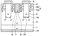
図1に示すSiC半導体装置は、セル領域にトレンチゲート構造の縦型MOSFETが形成され、図示していないが、セル領域を囲む外周領域に外周耐圧構造が備えられた構成とされている。 The SiC semiconductor device shown in FIG. 1 has a structure in which a vertical MOSFET having a trench gate structure is formed in a cell region, and although not shown, an outer peripheral withstand voltage structure is provided in an outer peripheral region surrounding the cell region.
SiC半導体装置は、SiCからなる高濃度不純物層を構成するn+型基板1の表面側に、n+型基板1よりも低不純物濃度のSiCからなるn-型ドリフト層2が形成された半導体基板を用いて形成されている。n+型基板1は、例えばn型不純物濃度が1.0×10¹⁹/cm3とされ、表面が(0001)Si面とされている。n-型ドリフト層2は、例えばn型不純物濃度が0.5〜2.0×1016/cm3とされている。
The SiC semiconductor device has a semiconductor in which an n − -
n-型ドリフト層2の上層部にはベース領域3が形成されている。本実施形態の場合、ベース領域3は、n-型ドリフト層2よりも高不純物濃度のp型SiCで構成されており、p型不純物濃度が比較的高くされた高濃度ベース領域3aと、それよりもp型不純物濃度が低くされた低濃度ベース領域3bとが順に積層された構造とされている。
高濃度ベース領域3aは、例えばp型不純物濃度が5×10¹⁷/cm3以上、例えば1×1018/cm3とされ、厚みが50〜200nmとされている。低濃度ベース領域3bは、例えばp型不純物濃度が1.0×1016/cm3以下とされ、厚みが0.3〜1.0μmとされている。
The high
さらに、ベース領域3の上層部分にはn+型ソース領域4が形成されている。また、n+型ソース領域4の表面からn+型ソース領域4およびベース領域3を貫通し、n-型ドリフト層2に達するようにp型ディープ層5が形成されている。具体的には、n+型ソース領域4の表面からn+型ソース領域4およびベース領域3を貫通し、n-型ドリフト層2に達するディープトレンチ15が形成されており、このディープトレンチ15内にp型ディープ層5が埋め込まれている。例えば、ディープトレンチ15は、アスペクト比が2以上の深さとされている。さらに、p型ディープ層5の底部の角部、換言すればディープトレンチ15の底部における角部に、n-型領域16が備えられている。
Further, an n +
n+型ソース領域4は、後述するトレンチゲート構造の両側に配置されており、p型ディープ層5は、n+型ソース領域4を挟んでトレンチゲート構造と反対側においてトレンチゲート構造よりも深い位置まで形成されており、n-型領域16を覆いつつディープトレンチ15内を埋め込むように形成されている。n+型ソース領域4は、表層部におけるn型不純物濃度が例えば2.5×10¹⁸〜1.0×10¹⁹/cm3、厚さ0.5μm程度で構成されている。また、p型ディープ層5は、ベース領域3よりも高不純物濃度とされ、p型不純物濃度が例えば1.0×1017〜1.0×1019/cm3とされている。本実施形態では、p型ディープ層5は、後述するソース電極9と電気的接続が行われるコンタクト領域も兼ねている。n-型領域16は、ベース領域3よりも下方において、ベース領域3から離れて形成されている。n-型領域16は、断面形状が三角形状、もしくはp型ディープ層5と接する部分が凹んで曲面となった三角ラウンド形状とされており、n型不純物濃度がn-型ドリフト層2よりも高く、例えば1.0×1016〜4.0×1016/cm3とされている。このようなn-型領域16が形成されることにより、p型ディープ層5の底部側の角部の断面形状が垂直もしくは鋭角にはならず、鈍角もしくは丸みを帯びた形状となっている。
The n + -
また、ベース領域3およびn+型ソース領域4を貫通してn-型ドリフト層2に達するように、紙面垂直方向を長手方向とするトレンチ6が形成されている。このトレンチ6の側面と接するように上述したベース領域3における高濃度ベース領域3aや低濃度ベース領域3bおよびn+型ソース領域4が配置されている。
Further, a
さらに、ベース領域3のうちn+型ソース領域4とn-型ドリフト層2との間に位置する部分の表層部をチャネル領域として、このチャネル領域を含むトレンチ6の内壁面にはゲート絶縁膜7が形成されている。そして、ゲート絶縁膜7の表面にはドープドPoly−Siにて構成されたゲート電極8が形成されており、これらゲート絶縁膜7およびゲート電極8によってトレンチ6内が埋め尽くされている。
Further, a surface layer portion of the
このようにして、トレンチゲート構造が構成されている。このトレンチゲート構造は、図1の紙面垂直方向を長手方向として延設されており、複数のトレンチゲート構造が図1中の左右方向に並べられることでストライプ状とされている。また、上述したn+型ソース領域4およびp型ディープ層5もトレンチゲート構造の長手方向に沿って延設されたレイアウト構造とされている。
Thus, a trench gate structure is formed. The trench gate structure extends in a direction perpendicular to the paper surface of FIG. 1 as a longitudinal direction, and is formed in a stripe shape by arranging a plurality of trench gate structures in the left-right direction in FIG. Further, the above-described n + -
また、n+型ソース領域4およびp型ディープ層5の表面やゲート電極8の表面には、ソース電極9やゲート配線(図示せず)が形成されている。ソース電極9およびゲート配線は、複数の金属(例えばNi/Al等)にて構成されている。そして、複数の金属のうち少なくともn型SiC(具体的にはn+型ソース領域4やn型ドープの場合のゲート電極8)と接触する部分はn型SiCとオーミック接触可能な金属で構成されている。また、複数の金属のうち少なくともp型SiC(具体的にはp型ディープ層5)と接触する部分はp型SiCとオーミック接触可能な金属で構成されている。なお、これらソース電極9およびゲート配線は、図示しない層間絶縁膜上に形成されることで電気的に絶縁されている。そして、層間絶縁膜に形成されたコンタクトホールを通じて、ソース電極9はn+型ソース領域4およびp型ディープ層5と電気的に接触させられ、ゲート配線はゲート電極8と電気的に接触させられている。
A
さらに、n+型基板1の裏面側にはn+型基板1と電気的に接続されたドレイン電極10が形成されている。このような構造により、nチャネルタイプの反転型のトレンチゲート構造の縦型MOSFETが構成されている。そして、この縦型MOSFETが形成されたセル領域の外周領域に、図示しない外周耐圧構造が備えられることで、本実施形態にかかるSiC半導体装置が構成されている。
Further, on the back side of the n + -type substrate 1 n + -
このようなSiC半導体装置に備えられる反転型のトレンチゲート構造の縦型MOSFETは、ゲート電極8にゲート電圧を印加すると、ベース領域3のうちトレンチ6に接している表面にチャネルが形成される。これにより、ソース電極9から注入された電子がn+型ソース領域4からベース領域3に形成されたチャネルを通った後、n-型ドリフト層2に到達し、ソース電極9とドレイン電極10との間に電流を流すという動作が行われる。
When a gate voltage is applied to the
このとき、本実施形態のSiC半導体装置では、ディープトレンチ15をすべてp型ディープ層5によって埋め込んでしまうのではなく、ディープトレンチ15の底部における角部をn-型領域16としている。このため、n-型領域16が形成されることにより、p型ディープ層5の底部側の角部の断面形状が垂直もしくは鋭角にはならず、鈍角もしくは丸みを帯びた形状となる。これにより、p型ディープ層5の底部側の角部においてオフ時に電界集中によって電界強度が高くなることを抑制できる。したがって、縦型MOSFETの耐圧低下を抑制することが可能となる。そして、このようにn-型領域16を形成することによって縦型MOSFETの耐圧低下を抑制できることから、p型ディープ層5を必要以上に深く形成しなくても済み、オン抵抗の増大を抑制することが可能となる。
At this time, in the SiC semiconductor device of the present embodiment, the
また、ベース領域3を高濃度ベース領域3aと低濃度ベース領域3bによって構成しており、これら高濃度ベース領域3aと低濃度ベース領域3bによってチャネルが形成されるようにしている。このため、高濃度ベース領域3aによってベース領域3内における空乏層の拡がりを抑制できる。したがって、ベース領域3内が完全空乏化してパンチスルーしてしまうことを防止でき、素子耐圧確保が可能になると共にトレンチ6の底部のゲート絶縁膜7の劣化防止も可能になる。また、閾値電圧が高濃度ベース領域3aのp型不純物濃度に依存することになるため、高閾値電圧を得ることも可能となる。
The
また、低濃度ベース領域3bの部分においてチャネル移動度が高められるため、高濃度ベース領域3aを備えていたとしても、オン抵抗低減を図ることが可能となる。したがって、オン抵抗低減および素子耐圧確保が可能で、かつ、高閾値電圧が得られるトレンチゲート構造の縦型MOSFETとすることができる。
Further, since the channel mobility is increased in the low
また、高濃度ベース領域3aが存在することで、オフ時においては、n-型ドリフト層2とベース領域3との接合から発生するキャリアの引き抜き効果が高められるため、ドレインリーク電流を低減できる。
In addition, the presence of the high-
また、ベース領域3のうちn-型ドリフト層2と接触する部分がすべてp型不純物濃度が高い高濃度ベース領域3aとされていることから、n-型ドリフト層2とベース領域3とのPN接合にて構成される内蔵ダイオードに電流が流れる際の立上り電圧が低減できる。このため、内蔵ダイオードのオン電圧が低減され、内蔵ダイオードを積極的に用いた同期整流駆動時の損失低減を図ることも可能となる。
Further, since all the portions of the
さらに、オフ時において、高濃度ベース領域3a側からn-型ドリフト層2側に延びる空乏層によって、トレンチゲート構造の下方に等電位線が入り込み難くなるようにできる。このため、トレンチ6の底面においてゲート絶縁膜7に印加される電界集中を緩和でき、ゲート絶縁膜7の寿命向上、逆バイアス寿命向上を図ることが可能となる。
Further, at the time of off, the depletion layer extending from the high-
続いて、図1のように構成された本実施形態にかかるSiC半導体装置の製造方法について、図2および図3を参照して説明する。 Subsequently, a method of manufacturing the SiC semiconductor device according to the present embodiment configured as shown in FIG. 1 will be described with reference to FIGS.
〔図2(a)に示す工程〕
まず、半導体基板として、SiCからなるn+型基板1の表面上にSiCからなるn-型ドリフト層2がエピタキシャル成長させられた、いわゆるエピ基板を用意する。そして、このエピ基板をエピタキシャル成長装置内に配置し、n-型ドリフト層2の表面に高濃度ベース領域3a、低濃度ベース領域3b、n+型ソース領域4を順にエピタキシャル成長する。
[Step shown in FIG. 2 (a)]
First, as a semiconductor substrate, a so-called epi substrate in which an n −
〔図2(b)に示す工程〕
n+型ソース領域4の表面にマスク材(図示せず)を配置したのち、フォトリソグラフィによってマスク材のうちのp型ディープ層5およびn-型領域16の形成予定位置を開口させる。そして、マスク材を配置した状態でRIE(Reactive Ion Etching)などの異方性エッチングを行うことで、p型ディープ層5およびn-型領域16の形成予定位置にディープトレンチ15を形成する。
[Step shown in FIG. 2 (b)]
After arranging a mask material (not shown) on the surface of n + -
〔図2(c)、(d)に示す工程〕
図示しないエピタキシャル成長装置を用いて、図2(c)に示すn-型領域16を形成する工程と、図2(d)に示すp型ディープ層15を形成する工程を連続して行う。
[Steps shown in FIGS. 2C and 2D]
Using an epitaxial growth apparatus (not shown), the step of forming the n − -
具体的には、図3に示すように、まず昇温期間としてエピタキシャル成長装置内の温度を例えば1650℃まで上昇させる。昇温期間については、例えば40分以内程度の時間としている。また、このときにn型ドーパントを含むドーパントガスを導入する。その後、n型ドーパントを含むドーパントガスからp型ドーパントを含むドーパントガスに切替えると共にSiC原料ガスを導入することでn-型領域16を形成しつつp型ディープ層5をエピタキシャル成長させる。
Specifically, as shown in FIG. 3, first, the temperature in the epitaxial growth apparatus is raised to, for example, 1650 ° C. as a temperature raising period. The heating period is, for example, about 40 minutes or less. At this time, a dopant gas containing an n-type dopant is introduced. After that, the p-type
SiC原料ガスとしては、例えばSi原料となるシラン(SiH4)やC原料となるプロパン(C3H8)等を用いることができる。また、p型ディープ層5を形成する際のドーパントガスとしては、p型ドーパントを含むTMA(トリメチルアルミニウム)を用いている。また、n-型領域16を形成する際のドーパントガスとしては、n型ドーパントとなる窒素(N2)を用いている。さらに、必要に応じて、エッチングガスとして、例えば水素(H2)も導入している。
As the SiC source gas, for example, silane (SiH 4 ) serving as a Si source, propane (C 3 H 8 ) serving as a C source, or the like can be used. As a dopant gas for forming the p-type
このとき、SiC原料ガスを導入する前に窒素を導入しておくと、雰囲気中への昇華などによって存在するSi元素やC元素に基づいて、もしくは、SiC原料ガスが導入された初期時に、ディープトレンチ15の底部にn-型領域16を形成することができる。このときのn-型領域16の形成はp型ディープ層5の形成よりも前に行われ、n-型領域16が形成されてからp型ディープ層5が形成されるようにできる。特に、p型ドーパントのように有機金属材料がドーパントとされる場合、そのドーパントがガス導入初期時にエピタキシャル成長装置のチャンバ内壁面に貼り付いて所望のp型不純物濃度となるまでに時間が掛かる立上り遅れが発生する。このため、n-型領域16がより容易に形成されるようにできる。さらに、エッチングガスを導入しつつエピタキシャル成長装置のチャンバ内の昇温を行っているため、昇温期間中にはエッチングとSiCデポジションの平衡状態となる。その昇温期間中からn型ドーパントを導入していることから、より的確にディープトレンチ15の角部にのみn-型領域16が形成されるようにできる。
At this time, if nitrogen is introduced before the introduction of the SiC raw material gas, deep nitrogen is introduced based on the Si element or C element present due to sublimation into the atmosphere or at the initial stage when the SiC raw material gas is introduced. An n − -
そして、研削やCMP(Chemical Mechanical Polishing)などによる平坦化によって、p型ディープ層5の形成の際にn+型ソース領域4の上に形成されたp型不純物層を除去し、n+型ソース領域4の表面を露出させる。これにより、ディープトレンチ15内にのみn-型領域16やp型ディープ層5が配置された構造が形成される。
Then, the flattening due to grinding or CMP (Chemical Mechanical Polishing), to remove p-type impurity layer formed on the n + -
〔図2(e)に示す工程〕
n+型ソース領域4やp型ディープ層5の表面にマスク材(図示せず)を配置したのち、フォトリソグラフィによってマスク材のうちのトレンチ6の形成予定位置を開口させる。そして、マスク材を配置した状態でRIEなどの異方性エッチングを行うことにより、セル領域においてトレンチ6を形成する。その後、マスク材を除去する。
[Step shown in FIG. 2 (e)]
After a mask material (not shown) is disposed on the surface of the n +
そして、必要に応じて、1600度以上の減圧下における水素雰囲気、例えば1625℃、2.7×10⁴Pa(=200Torr)の高温水素雰囲気での熱処理による水素エッチングを実施する。この水素エッチングによってトレンチ6の内壁面の丸め処理が行われ、トレンチ6の開口入口やコーナー部を丸められると共に、トレンチエッチングのダメージ除去が行われる。
Then, if necessary, hydrogen etching is performed by heat treatment in a hydrogen atmosphere under a reduced pressure of 1600 degrees or more, for example, a high-temperature hydrogen atmosphere of 1625 ° C. and 2.7 × 10 4 Pa (= 200 Torr). By this hydrogen etching, the inner wall surface of the
〔図2(f)に示す工程〕
ウェット雰囲気による熱酸化によってゲート絶縁膜7を形成したのち、ゲート絶縁膜7の表面にドープドPoly−Si層を成膜し、このドープドPoly−Si層をパターニングすることでトレンチ6内に残し、ゲート電極8を形成する。
[Step shown in FIG. 2 (f)]
After the
この後の工程については、従来と同様である。すなわち、層間絶縁膜の形成工程、フォト・エッチングによるコンタクトホール形成工程、電極材料をデポジションしたのちパターニングすることでソース電極9やゲート配線層を形成する工程、n+型基板1の裏面にドレイン電極10を形成する工程等を行う。これにより、図1に示すトレンチゲート構造の縦型MOSFETがセル領域に備えられたSiC半導体装置が完成する。
Subsequent steps are the same as in the related art. That is, a step of forming an interlayer insulating film, a step of forming a contact hole by photo-etching, a step of forming a
以上説明したように、本実施形態で説明した反転型のトレンチゲート構造の縦型MOSFETを備えたSiC半導体装置では、p型ディープ層5の底部側の角部、つまりディープトレンチ15における底部側の角部にn-型領域16が形成されるようにしている。このため、p型ディープ層5の底部側の角部の断面形状を鈍角もしくは丸みを帯びた形状にできる。これにより、p型ディープ層5の底部側の角部においてオフ時に電界集中によって電界強度が高くなることを抑制できる。したがって、縦型MOSFETの耐圧低下を抑制することが可能となる。そして、このようにn-型領域16を形成することによって縦型MOSFETの耐圧低下を抑制できることから、p型ディープ層5を必要以上に深く形成しなくても済み、オン抵抗の増大を抑制することが可能となる。
As described above, in the SiC semiconductor device including the vertical MOSFET having the inverted trench gate structure described in the present embodiment, the bottom corner of the p-type
(第2実施形態)
第2実施形態について説明する。本実施形態は、第1実施形態に対してp型ディープ層5およびn-型領域16の製造プロセスを変更したものであり、その他については第1実施形態と同様であるため、第1実施形態と異なる部分についてのみ説明する。
(2nd Embodiment)
A second embodiment will be described. This embodiment is different from the first embodiment in the manufacturing process of the p-type
本実施形態では、p型ディープ層5およびn-型領域16の形成の際におけるn型ドーパントを含むドーパントガスとp型ドーパントを含むドーパントガスの導入のタイミングを第1実施形態に対して変更している。
In the present embodiment, the timing of introducing the dopant gas containing the n-type dopant and the dopant gas containing the p-type dopant during the formation of the p-type
具体的には、図4に示すように、昇温期間中にn型ドーパントを含むドーパントガスを導入しているが、その後、SiC原料ガスを導入する前に、n型ドーパントを含むドーパントガスからp型ドーパントを含むドーパントガスに切替えている。そして、ドーパントガスの切替えが終わってから、SiC原料ガスの導入を行うようにしている。 Specifically, as shown in FIG. 4, a dopant gas containing an n-type dopant is introduced during the temperature rising period, and thereafter, before introducing the SiC source gas, the dopant gas containing the n-type dopant is introduced. The mode is switched to a dopant gas containing a p-type dopant. Then, after the switching of the dopant gas is completed, the introduction of the SiC raw material gas is performed.
このように、ドーパントガスの切替えをSiC原料ガスの導入前に行い、SiC原料ガスの導入前からp型ドーパントを含むドーパントガスが導入されるようにしても良い。これにより、SiC原料ガスが導入される前に、エピタキシャル成長装置のチャンバ内壁面に貼り付くようにできることから、SiC原料ガス導入後に貼りつくp型ドーパントの量を低減できる。したがって、より早くからp型ディープ層5が形成されるようにでき、n-型領域16の形成される範囲の縮小を図ることが可能となる。
As described above, the switching of the dopant gas may be performed before the introduction of the SiC raw material gas, and the dopant gas containing the p-type dopant may be introduced before the introduction of the SiC raw material gas. Thereby, before the introduction of the SiC source gas, it can be attached to the inner wall surface of the chamber of the epitaxial growth apparatus, so that the amount of the p-type dopant attached after the introduction of the SiC source gas can be reduced. Therefore, p-type
(第2実施形態の変形例)
上記第2実施形態では、SiC原料ガスの導入前に、ドーパントガスの切替えを行うようにしているが、逆に、図5に示すように、SiC原料ガスの導入後にドーパントガスの切替えを行うようにすることもできる。このようにすれば、より遅くからp型ディープ層5が形成されるようにでき、n-型領域16の形成される範囲の拡大を図ることが可能となる。
(Modification of Second Embodiment)
In the second embodiment, the switching of the dopant gas is performed before the introduction of the SiC raw material gas. On the contrary, as shown in FIG. 5, the switching of the dopant gas is performed after the introduction of the SiC raw material gas. You can also By doing so, the p-type
(第3実施形態)
第3実施形態について説明する。本実施形態は、第1実施形態に対してp型ディープ層5の構成を変更したものであり、その他については第1実施形態と同様であるため、第1実施形態と異なる部分についてのみ説明する。
(Third embodiment)
A third embodiment will be described. In the present embodiment, the configuration of the p-type
図6に示すように、本実施形態のSiC半導体装置に備えられる縦型MOSFETでは、p型ディープ層5を二層構造としており、第1実施形態で説明したp型ディープ層5を上方p型ディープ層5aとして、この上方p型ディープ層5aおよびn-型領域16の下方に、さらに下方p型ディープ層5aを備えた構造としている。下方p型ディープ層5bは、上方p型ディープ層5aと繋がっており、これらは共にソース電位とされる。また、下方p型ディープ層5bは、その底部の角部が丸まった形状となっている。
As shown in FIG. 6, in the vertical MOSFET provided in the SiC semiconductor device of the present embodiment, the p-type
このように、p型ディープ層5を上方p型ディープ層5aと下方p型ディープ層5bの二層構造によって実現することもできる。このような構造とする場合においても、下方p型ディープ層5bの底部の角部が丸まっていることから、電界集中を抑制できて、上記第1実施形態と同様の効果を得ることができる。
As described above, the p-type
また、このような構造とする場合、p型ディープ層5の側面にn-型領域16が形成された構造になることから、この部分においてp型ディープ層5よりn-型ドリフト層2側に伸びる空乏層の伸びを抑制することが可能となる。したがって、空乏層の伸びを抑制できる分、JFET部の空乏化領域を縮小することができ、電流経路が広がるようにできるため、オン抵抗の低減を図ることが可能となる。
Further, in the case of such a structure, since the n − -
なお、本実施形態にかかる縦型MOSFETの製造方法は、基本的には第1実施形態と同様である。ただし、ディープトレンチ15を形成した後に、例えばディープトレンチ15を形成する際に用いたマスクをそのまま用いてp型ドーパントのイオン注入を行うことで下方p型ディープ層5bを形成する工程を行うようにする必要がある。このようにイオン注入を行うことによって下方p型ディープ層5bを形成すると、下方p型ディープ層5bの底部の角部が丸まった形状になるようにできる。
The method of manufacturing the vertical MOSFET according to the present embodiment is basically the same as that of the first embodiment. However, after the
(第4実施形態)
第4実施形態について説明する。本実施形態では、半導体素子として縦型MOSFETに代えて縦型のJBSを備えたSiC半導体装置について説明する。
(Fourth embodiment)
A fourth embodiment will be described. In the present embodiment, a description will be given of a SiC semiconductor device including a vertical JBS instead of a vertical MOSFET as a semiconductor element.
図7に示すように、本実施形態のSiC半導体装置も、SiCからなる高濃度不純物層を構成するn+型基板41の表面側に、n+型基板41よりも低不純物濃度のSiCからなるn-型ドリフト層42が形成された半導体基板を用いて形成されている。この半導体基板としては、第1実施形態と同様のものを用いている。
As shown in FIG. 7, the SiC semiconductor device of the present embodiment is also formed of SiC having a lower impurity concentration than the n + type substrate 41 on the surface side of the n + type substrate 41 constituting the high concentration impurity layer made of SiC. It is formed using the semiconductor substrate on which the n −
n-型ドリフト層42の上には、n-型ドリフト層2よりも高不純物濃度とされたn型層43が形成されている。また、n型層43を貫通してn-型ドリフト層2に達するようにディープトレンチ44が形成され、このディープ層45が形成されていると共に、ディープ層45の角部、つまりディープトレンチ44の底部の角部にn-型領域46が形成されている。
On n − -
さらに、n型層43やディープ層45の上には、これらと接触するようにショットキー電極47が形成されている。そして、n+型基板41の裏面側、つまりn-型ドリフト層42と反対側に裏面電極に相当するオーミック電極48が備えられることで、図7に示す縦型JBSを備えたSiC半導体装置が構成されている。
Further, a
このように、JBSを備えたSiC半導体装置においても、p型ディープ層45の角部にn-型領域46を備えることで、p型ディープ層45の底部側の角部の断面形状が垂直もしくは鋭角にはならず、鈍角もしくは丸みを帯びた形状となる。これにより、p型ディープ層45の底部側の角部においてオフ時に電界集中によって電界強度が高くなることを抑制できる。したがって、耐圧低下を抑制できることから、p型ディープ層45を必要以上に深く形成しなくても済み、オン抵抗の増大を抑制することが可能となる。
As described above, even in the SiC semiconductor device provided with the JBS, by providing the n − -
続いて、図7のように構成された本実施形態にかかるSiC半導体装置の製造方法について、図8を参照して説明する。 Subsequently, a method for manufacturing the SiC semiconductor device according to the present embodiment configured as shown in FIG. 7 will be described with reference to FIG.
〔図8(a)に示す工程〕
まず、半導体基板として、SiCからなるn+型基板41の表面上にSiCからなるn-型ドリフト層42がエピタキシャル成長させられた、いわゆるエピ基板を用意する。
[Step shown in FIG. 8A]
First, as a semiconductor substrate, a so-called epi substrate in which an n − type drift layer made of SiC is epitaxially grown on a surface of an n + type substrate 41 made of SiC is prepared.
〔図8(b)に示す工程〕
n-型ドリフト層42の表面にマスク材49を配置したのち、フォトリソグラフィによってマスク材49のうちのp型ディープ層45およびn-型領域46の形成予定位置を開口させる。そして、マスク材49を配置した状態でRIEなどの異方性エッチングを行うことで、p型ディープ層45およびn-型領域46の形成予定位置にディープトレンチ44を形成する。
[Step shown in FIG. 8B]
After arranging the
〔図8(c)に示す工程〕
マスク材49を除去したのち、図2(c)、(d)と同様の工程を行う。これにより、ディープトレンチ44内がp型ディープ層45およびn-型領域46によって埋め込まれる。
[Step shown in FIG. 8C]
After removing the
〔図8(d)に示す工程〕
n型層43の表面上に形成されたp型ディープ層45を構成するp型SiC層を研削やCMPなどによって除去し、n型層43を露出させる。
[Step shown in FIG. 8D]
The p-type SiC layer constituting the p-type
この後の工程については図示しないが、n型層43やp型ディープ層45の表面上にショットキー電極47を形成する工程と、n+型基板41の裏面上にオーミック電極48を形成する工程を行うことで、図7に示す縦型JBSがに備えられたSiC半導体装置が完成する。
Although not shown in the subsequent steps, a step of forming a
以上説明したように、縦型JBSを備えるSiC半導体装置に対しても、p型ディープ層45およびn-型領域46を備える構造を適用することができる。
As described above, the structure including the p-type
(他の実施形態)
本発明は上記した実施形態に限定されるものではなく、特許請求の範囲に記載した範囲内において適宜変更が可能である。
(Other embodiments)
The present invention is not limited to the embodiments described above, and can be appropriately modified within the scope described in the claims.
例えば、上記各実施形態では、n+型ソース領域4をエピタキシャル成長によって形成しているが、n+型ソース領域4についてはベース領域3の上層部に形成されていれば良いため、イオン注入などの他の手法によって形成することもできる。
For example, in each of the above embodiments, the n + -
また、第2実施形態では、ベース領域3を高濃度ベース領域3aと低濃度ベース領域3bに分けたが、単一の不純物濃度で構成しても良い。また、不純物濃度を異ならせる構成では、高濃度ベース領域3aと低濃度ベース領域3bの境界部において不純物濃度が徐々に変化し、その境界部を挟んでp型不純物濃度が異なった高濃度ベース領域3aと低濃度ベース領域3bとが積層された形態でも良い。また、低濃度ベース領域3bについては、ノンドープ(つまり、ほとんどp型ドーパントがドープされていない)であるi型半導体によって構成されていても構わない。例えば、低濃度ベース領域3bのドープ量について、エピタキシャル成長時に雰囲気中に残留しているp型ドーパントがドープされる程度とすることができる。その場合、低濃度ベース領域3bでの高チャネル移動度化を更に実現することが可能となり、更なる低オン抵抗化が可能になる。
Further, in the second embodiment, the
さらに、上記各実施形態では、裏面側が高不純物濃度の裏面層、表面側がそれよりも低不純物濃度なドリフト層とされた半導体基板として、n+型基板1の表面にn-型ドリフト層2を形成した構造を例に挙げて説明した。しかしながら、これは半導体基板の一例を示したに過ぎず、例えばn-型ドリフト層2にて構成される基板の裏面側にn型ドーパントをイオン注入すること、もしくはエピタキシャル成長によって裏面層を構成した半導体基板であっても良い。
Furthermore, in each of the above embodiments, the n −
また、上記第4実施形態では、第1実施形態の構造および製造方法と同様のp型ディープ層45およびn-型領域46を例に挙げて説明したが、第2実施形態およびその変形例と同様の製造方法、第3実施形態と同様の構造および製造方法を適用することもできる。
In the fourth embodiment, the p-type
また、上記各実施形態では、第1導電型をn型、第2導電型をp型としたnチャネルタイプの縦型MOSFETを例に挙げて説明したが、各構成要素の導電型を反転させたpチャネルタイプの縦型MOSFETに対しても本発明を適用することができる。その場合、半導体基板の表面の面方位を(000−1)カーボン面とすることで、ディープトレンチの側面にはp型の制限層を優位にエピタキシャル成長させられ、ディープトレンチの底部にはn型のディープ層を優位にエピタキシャル成長させることができる。 Further, in each of the above embodiments, an n-channel type vertical MOSFET in which the first conductivity type is n-type and the second conductivity type is p-type has been described as an example, but the conductivity type of each component is reversed. The present invention can also be applied to a p-channel type vertical MOSFET. In this case, by setting the plane orientation of the surface of the semiconductor substrate to the (000-1) carbon plane, the p-type limiting layer can be epitaxially grown on the side surface of the deep trench dominantly, and the n-type limiting layer can be formed on the bottom of the deep trench. The deep layer can be predominantly epitaxially grown.
さらに、上記各実施形態では、化合物半導体としてSiCを例に挙げ、ディープトレンチ内に第2導電型のディープ層をエピタキシャル成長させる一例として下地層となるn-型ドリフト層2の上にp型ディープ層5を形成する場合を例に挙げて説明した。しかしながら、これも単なる一例を示したに過ぎない。すなわち、化合物半導体にて構成される第1導電型の下地層に対してディープトレンチを形成し、そのディープトレンチに第2導電型の化合物半導体にて構成されるディープ層をエピタキシャル成長する構造について、本発明を適用することができる。
Further, in each of the above embodiments, SiC is taken as an example of a compound semiconductor, and a p-type deep layer is formed on an n − -
なお、結晶の方位を示す場合、本来ならば所望の数字の上にバー(−)を付すべきであるが、電子出願に基づく表現上の制限が存在するため、本明細書においては、所望の数字の前にバーを付すものとする。 In addition, when indicating the orientation of the crystal, a bar (-) should normally be added to a desired number. However, since there is a restriction on expression based on the electronic application, in this specification, a desired number is indicated. A bar shall precede the number.
1、41 n+型基板
2、42 n-型ドリフト層
3 ベース領域
4 n+型ソース領域
5、45 p型ディープ層
6 トレンチ
8 ゲート電極
16、46 n-型領域
15、44 ディープトレンチ
1, 41 n + type substrate 2, 42 n −
Claims (13)
化合物半導体にて構成される第1導電型の下地層(2、42)を有する半導体基板(1、2、41、42)と、
前記下地層に対して形成されたディープトレンチ(15、44)の底部における角部に形成された第1導電型領域(16、46)と、
前記ディープトレンチ内において前記第1導電型領域を覆うように形成された第2導電型のディープ層(5、45)と、を有し、
前記第1導電型領域は、断面形状が三角形状もしくは前記ディープ層と接する部分が凹んで曲面となった三角ラウンド形状とされている化合物半導体装置。 A compound semiconductor device,
A semiconductor substrate (1, 2, 41, 42) having a first conductivity type underlayer (2, 42) made of a compound semiconductor;
A first conductivity type region (16, 46) formed at a corner at the bottom of the deep trench (15, 44) formed with respect to the underlayer;
A second conductivity type deep layer (5, 45) formed to cover the first conductivity type region in the deep trench;
The compound semiconductor device according to claim 1, wherein the first conductivity type region has a triangular cross section or a triangular round shape in which a portion in contact with the deep layer is concave and curved.
前記ドリフト層の上に形成された第2導電型のベース領域(3)と、
前記ベース領域の上層部に形成され、前記ドリフト層よりも高不純物濃度の第1導電型のソース領域(4)と、
前記ソース領域の表面から前記ベース領域よりも深くまで形成されたゲートトレンチ(6)内に形成され、該ゲートトレンチの内壁面に形成されたゲート絶縁膜(7)と、前記ゲート絶縁膜の上に形成されたゲート電極(8)と、を有して構成されたトレンチゲート構造と、
前記ソース領域に電気的に接続されるソース電極(9)と、
前記半導体基板の裏面側における前記裏面層と電気的に接続されるドレイン電極(10)と、を有する縦型MOSFETを備え、
前記ソース領域および前記ベース領域を貫通して前記ドリフト層に至り、かつ、前記ゲートトレンチよりも深い位置まで前記ディープトレンチ(15)が形成され、該ディープトレンチ内における前記ベース領域よりも下方に、前記ベース領域から離れて前記第1導電型領域(16)が形成されていると共に、該ディープトレンチ内において前記第1導電型領域を覆うように前記ディープ層(5)が形成されている請求項1または2に記載の化合物半導体装置。 A back layer (1) provided on the back side and having a high impurity concentration; and a first conductivity type drift layer (2) provided on the front side and constituting the underlayer and having a lower impurity concentration than the back layer. The semiconductor substrate (1, 2) having:
A second conductivity type base region (3) formed on the drift layer;
A first conductivity type source region (4) formed in an upper layer of the base region and having a higher impurity concentration than the drift layer;
A gate insulating film (7) formed in a gate trench (6) formed from the surface of the source region to a depth deeper than the base region, and formed on an inner wall surface of the gate trench; A gate electrode (8) formed in the trench gate structure,
A source electrode (9) electrically connected to the source region;
A vertical MOSFET having a drain electrode (10) electrically connected to the back surface layer on the back surface side of the semiconductor substrate;
The deep trench (15) is formed to reach the drift layer through the source region and the base region and to a position deeper than the gate trench, and in the deep trench below the base region, The first conductivity type region (16) is formed apart from the base region, and the deep layer (5) is formed to cover the first conductivity type region in the deep trench. 3. The compound semiconductor device according to 1 or 2.
前記ドリフト層の上に形成され、前記ドリフト層よりも高不純物濃度となる第1導電型高濃度層(43)と、を有するジャンクションバリアダイオードを備え、
前記第1導電型高濃度層を貫通し、前記ドリフト層に達するように前記ディープトレンチ(44)が形成され、該ディープトレンチ内における底部の角部に前記第1導電型領域(46)が形成されていると共に、該ディープトレンチ内において前記第1導電型領域を覆うように前記ディープ層(45)が形成されている請求項1または2に記載の化合物半導体装置。 A backside layer (41) provided on the backside and having a high impurity concentration, and a first conductivity type drift layer (42) provided on the frontside and constituting the base layer and having a lower impurity concentration than the backside layer. The semiconductor substrate (41, 42) having:
A first-conductivity-type high-concentration layer (43) formed on the drift layer and having a higher impurity concentration than the drift layer;
The deep trench (44) is formed so as to penetrate the first conductivity type high concentration layer and reach the drift layer, and the first conductivity type region (46) is formed at a bottom corner in the deep trench. 3. The compound semiconductor device according to claim 1, wherein said deep layer is formed so as to cover said first conductivity type region in said deep trench.
化合物半導体にて構成される第1導電型の下地層(2、42)を有する半導体基板(1、2、41、42)を用意することと、
前記下地層に対してディープトレンチ(15、44)を形成することと、
エピタキシャル成長装置内に第1導電型ドーパントを含むドーパントガスを導入しつつ、前記化合物半導体の原料ガスを導入し、前記ディープトレンチの底部における角部に、断面形状が三角形状もしくは表面が凹んで曲面となる三角ラウンド形状の第1導電型領域(16、46)を形成することと、
前記第1導電型領域を形成したのち、第2導電型ドーパントを含むドーパントガスを導入しつつ、前記化合物半導体の原料ガスを導入し、前記第1導電型領域を覆いつつ前記ディープトレンチ内に第2導電型のディープ層(5、45)をエピタキシャル成長させることと、を含む化合物半導体装置の製造方法。 A method for manufacturing a compound semiconductor device, comprising:
Preparing a semiconductor substrate (1, 2, 41, 42) having a first conductivity type underlayer (2, 42) composed of a compound semiconductor;
Forming deep trenches (15, 44) in the underlayer;
While introducing the dopant gas containing the first conductivity type dopant into the epitaxial growth apparatus, the source gas of the compound semiconductor is introduced, and the corner at the bottom of the deep trench has a triangular cross section or a curved surface with a concave surface. Forming first triangular round shaped first conductivity type regions (16, 46);
After forming the first conductivity type region, while introducing a dopant gas containing first conductivity type dopants, introducing a raw material gas of said compound semiconductor, the inside the deep trench while covering the first conductivity type region Epitaxially growing a two-conduction type deep layer (5, 45).
The step of forming the first conductivity type region and the step of epitaxially growing the deep layer include increasing the temperature in the epitaxial growth apparatus while introducing an etching gas for the compound semiconductor , and performing the second step during the temperature increase period. 7. The method according to claim 6, wherein a dopant gas containing one-conductivity-type dopant is introduced, and after the heating period, a dopant gas containing the second-conductivity-type dopant is introduced and a source gas for the compound semiconductor is introduced. The manufacturing method of the compound semiconductor device according to the above.
前記ディープトレンチを形成した後、該ディープトレンチの底部に対してイオン注入することで、第2導電型の下方ディープ層(5b)を形成することを含む請求項6ないし10のいずれか1つに記載の化合物半導体装置の製造方法。 The deep layer is defined as an upper deep layer (5a),
The method according to any one of claims 6 to 10, further comprising, after forming the deep trench, ion-implanting a bottom portion of the deep trench to form a lower deep layer (5b) of the second conductivity type. The manufacturing method of the compound semiconductor device according to the above.
前記ドリフト層(2)の上に第2導電型のベース領域(3)を形成することと、
前記ベース領域の上層部に、前記ドリフト層よりも高不純物濃度の第1導電型のソース領域(4)を形成することと、
前記ソース領域の表面から前記ベース領域よりも深くまでゲートトレンチ(6)を形成することと、
前記ゲートトレンチの内壁面にゲート絶縁膜(7)を形成すると共に、前記ゲート絶縁膜の上にゲート電極(8)を形成することでトレンチゲート構造を構成することと、
前記ソース領域に電気的に接続されるソース電極(9)を形成することと、
前記半導体基板の裏面側における前記裏面層と電気的に接続されるドレイン電極(10)を形成することと、を含み、
前記ディープトレンチを形成することとして、前記ソース領域の表面から前記ベース領域を貫通して前記ドリフト層に達し、かつ、前記ゲートトレンチより深い位置まで前記ディープトレンチ(15)を形成することを行い、
前記第1導電型領域を形成することとして、前記ディープトレンチ底部角部に前記第1導電型領域を形成する請求項6ないし11のいずれか1つに記載の化合物半導体装置の製造方法。 A back layer (1) provided on the back side, and a first conductivity type drift layer (2) provided on the front side and constituting the underlayer and having a lower impurity concentration than the back layer. Preparing the semiconductor substrate (1, 2);
Forming a second conductivity type base region (3) on the drift layer (2);
Forming a first conductivity type source region (4) having a higher impurity concentration than the drift layer in an upper layer portion of the base region;
Forming a gate trench (6) from the surface of the source region to a depth deeper than the base region;
Forming a trench gate structure by forming a gate insulating film (7) on the inner wall surface of the gate trench and forming a gate electrode (8) on the gate insulating film;
Forming a source electrode (9) electrically connected to the source region;
Forming a drain electrode (10) electrically connected to the back surface layer on the back surface side of the semiconductor substrate;
Forming the deep trench from the surface of the source region through the base region to the drift layer and forming the deep trench to a position deeper than the gate trench;
The method of manufacturing a compound semiconductor device according to claim 6, wherein forming the first conductivity type region includes forming the first conductivity type region at a bottom corner of the deep trench.
前記ドリフト層の上に、前記ドリフト層よりも高不純物濃度な第1導電型高濃度層(43)を形成することと、
前記第1導電型高濃度層に接触するショットキー電極(47)を形成することと、
前記裏面層に接触する裏面電極(48)を形成することと、を含み、
前記ディープトレンチを形成することとして、前記第1導電型高濃度層の表面から該第1導電型高濃度層を貫通して前記ドリフト層に達するように前記ディープトレンチ(44)を形成することを行う請求項6ないし11のいずれか1つに記載の化合物半導体装置の製造方法。 A back layer (41) provided on the back side and having a high impurity concentration; and a first conductivity type drift layer (42) provided on the front side and constituting the underlayer and having a lower impurity concentration than the back layer. The semiconductor substrate (41, 42) having:
Forming a first conductivity type high concentration layer (43) having a higher impurity concentration than the drift layer on the drift layer;
Forming a Schottky electrode (47) in contact with the first conductivity type high concentration layer;
Forming a back electrode (48) in contact with the back layer;
Forming the deep trench may include forming the deep trench (44) from a surface of the first conductivity type high concentration layer to penetrate the first conductivity type high concentration layer and reach the drift layer. 12. The method for manufacturing a compound semiconductor device according to claim 6, wherein the method is performed.
Priority Applications (4)
| Application Number | Priority Date | Filing Date | Title |
|---|---|---|---|
| JP2016032292A JP6651894B2 (en) | 2016-02-23 | 2016-02-23 | Compound semiconductor device and method of manufacturing the same |
| US16/070,061 US10643851B2 (en) | 2016-02-23 | 2017-01-12 | Compound semiconductor device and production method for the same |
| DE112017000947.2T DE112017000947T5 (en) | 2016-02-23 | 2017-01-12 | CONNECTING SEMICONDUCTOR DEVICE AND MANUFACTURING METHOD FOR THE CONNECTING SEMICONDUCTOR DEVICE |
| PCT/JP2017/000799 WO2017145548A1 (en) | 2016-02-23 | 2017-01-12 | Compound semiconductor device and production method for same |
Applications Claiming Priority (1)
| Application Number | Priority Date | Filing Date | Title |
|---|---|---|---|
| JP2016032292A JP6651894B2 (en) | 2016-02-23 | 2016-02-23 | Compound semiconductor device and method of manufacturing the same |
Publications (3)
| Publication Number | Publication Date |
|---|---|
| JP2017152489A JP2017152489A (en) | 2017-08-31 |
| JP2017152489A5 JP2017152489A5 (en) | 2018-06-21 |
| JP6651894B2 true JP6651894B2 (en) | 2020-02-19 |
Family
ID=59685318
Family Applications (1)
| Application Number | Title | Priority Date | Filing Date |
|---|---|---|---|
| JP2016032292A Active JP6651894B2 (en) | 2016-02-23 | 2016-02-23 | Compound semiconductor device and method of manufacturing the same |
Country Status (4)
| Country | Link |
|---|---|
| US (1) | US10643851B2 (en) |
| JP (1) | JP6651894B2 (en) |
| DE (1) | DE112017000947T5 (en) |
| WO (1) | WO2017145548A1 (en) |
Families Citing this family (5)
| Publication number | Priority date | Publication date | Assignee | Title |
|---|---|---|---|---|
| WO2018029796A1 (en) * | 2016-08-10 | 2018-02-15 | 日産自動車株式会社 | Semiconductor device |
| JP6673232B2 (en) * | 2017-01-17 | 2020-03-25 | 株式会社デンソー | Silicon carbide semiconductor device |
| JP7379880B2 (en) * | 2019-06-21 | 2023-11-15 | 富士電機株式会社 | semiconductor equipment |
| JP7354029B2 (en) * | 2020-03-13 | 2023-10-02 | 株式会社東芝 | Semiconductor device, semiconductor device manufacturing method, power supply circuit, and computer |
| JPWO2023199570A1 (en) * | 2022-04-14 | 2023-10-19 |
Family Cites Families (11)
| Publication number | Priority date | Publication date | Assignee | Title |
|---|---|---|---|---|
| JP4453671B2 (en) * | 2006-03-08 | 2010-04-21 | トヨタ自動車株式会社 | Insulated gate semiconductor device and manufacturing method thereof |
| JP4683075B2 (en) * | 2008-06-10 | 2011-05-11 | 株式会社デンソー | Silicon carbide semiconductor device and manufacturing method thereof |
| JP5482745B2 (en) * | 2011-08-10 | 2014-05-07 | 株式会社デンソー | Silicon carbide semiconductor device and manufacturing method thereof |
| JP5582112B2 (en) * | 2011-08-24 | 2014-09-03 | 株式会社デンソー | Silicon carbide semiconductor device and manufacturing method thereof |
| JP5884617B2 (en) * | 2012-04-19 | 2016-03-15 | 株式会社デンソー | Silicon carbide semiconductor device and manufacturing method thereof |
| JP5751213B2 (en) * | 2012-06-14 | 2015-07-22 | 株式会社デンソー | Silicon carbide semiconductor device and manufacturing method thereof |
| JP5834179B2 (en) * | 2013-04-16 | 2015-12-16 | パナソニックIpマネジメント株式会社 | Method for manufacturing silicon carbide semiconductor device |
| JP6048317B2 (en) | 2013-06-05 | 2016-12-21 | 株式会社デンソー | Silicon carbide semiconductor device |
| JP6341074B2 (en) * | 2014-01-24 | 2018-06-13 | 株式会社デンソー | Manufacturing method of semiconductor device |
| EP2977989B1 (en) | 2014-07-25 | 2019-05-08 | IMEC vzw | Sample-and-hold circuit for an interleaved analog-to-digital converter |
| US9768284B2 (en) * | 2015-03-05 | 2017-09-19 | Infineon Technologies Americas Corp. | Bipolar semiconductor device having a charge-balanced inter-trench structure |
-
2016
- 2016-02-23 JP JP2016032292A patent/JP6651894B2/en active Active
-
2017
- 2017-01-12 WO PCT/JP2017/000799 patent/WO2017145548A1/en active Application Filing
- 2017-01-12 DE DE112017000947.2T patent/DE112017000947T5/en active Pending
- 2017-01-12 US US16/070,061 patent/US10643851B2/en active Active
Also Published As
| Publication number | Publication date |
|---|---|
| US10643851B2 (en) | 2020-05-05 |
| WO2017145548A1 (en) | 2017-08-31 |
| DE112017000947T5 (en) | 2018-10-31 |
| US20190019680A1 (en) | 2019-01-17 |
| JP2017152489A (en) | 2017-08-31 |
Similar Documents
| Publication | Publication Date | Title |
|---|---|---|
| JP6048317B2 (en) | Silicon carbide semiconductor device | |
| JP6485382B2 (en) | Method of manufacturing compound semiconductor device and compound semiconductor device | |
| JP6572423B2 (en) | Semiconductor device and manufacturing method of semiconductor device | |
| JP5812029B2 (en) | Silicon carbide semiconductor device and manufacturing method thereof | |
| JP6428489B2 (en) | Silicon carbide semiconductor device and manufacturing method thereof | |
| JP6485383B2 (en) | Compound semiconductor device and method of manufacturing the same | |
| JP6651894B2 (en) | Compound semiconductor device and method of manufacturing the same | |
| JP6766512B2 (en) | Semiconductor devices and methods for manufacturing semiconductor devices | |
| JP2014146666A (en) | Semiconductor device | |
| JP2009302091A (en) | Silicon carbide semiconductor device, and method of manufacturing the same | |
| US20150115314A1 (en) | Semiconductor device and manufacturing method of the same | |
| US9660046B2 (en) | Method of manufacturing semiconductor device | |
| JP2019004010A (en) | Semiconductor device and manufacturing method for the same | |
| US9825125B2 (en) | Silicon carbide semiconductor device and manufacturing method of silicon carbide semiconductor device | |
| KR102100863B1 (en) | SiC MOSFET power semiconductor device | |
| JP6662092B2 (en) | Method for manufacturing compound semiconductor device |
Legal Events
| Date | Code | Title | Description |
|---|---|---|---|
| A521 | Request for written amendment filed |
Free format text: JAPANESE INTERMEDIATE CODE: A523 Effective date: 20180427 |
|
| A621 | Written request for application examination |
Free format text: JAPANESE INTERMEDIATE CODE: A621 Effective date: 20180427 |
|
| A131 | Notification of reasons for refusal |
Free format text: JAPANESE INTERMEDIATE CODE: A131 Effective date: 20190625 |
|
| A521 | Request for written amendment filed |
Free format text: JAPANESE INTERMEDIATE CODE: A523 Effective date: 20190823 |
|
| TRDD | Decision of grant or rejection written | ||
| A01 | Written decision to grant a patent or to grant a registration (utility model) |
Free format text: JAPANESE INTERMEDIATE CODE: A01 Effective date: 20191224 |
|
| A61 | First payment of annual fees (during grant procedure) |
Free format text: JAPANESE INTERMEDIATE CODE: A61 Effective date: 20200106 |
|
| R150 | Certificate of patent or registration of utility model |
Ref document number: 6651894 Country of ref document: JP Free format text: JAPANESE INTERMEDIATE CODE: R150 |
|
| R250 | Receipt of annual fees |
Free format text: JAPANESE INTERMEDIATE CODE: R250 |
|
| R250 | Receipt of annual fees |
Free format text: JAPANESE INTERMEDIATE CODE: R250 |