EP2803984A1 - Gassensor - Google Patents
Gassensor Download PDFInfo
- Publication number
- EP2803984A1 EP2803984A1 EP12864780.7A EP12864780A EP2803984A1 EP 2803984 A1 EP2803984 A1 EP 2803984A1 EP 12864780 A EP12864780 A EP 12864780A EP 2803984 A1 EP2803984 A1 EP 2803984A1
- Authority
- EP
- European Patent Office
- Prior art keywords
- gas
- gas sensor
- carbon nanotube
- ionic liquid
- source
- Prior art date
- Legal status (The legal status is an assumption and is not a legal conclusion. Google has not performed a legal analysis and makes no representation as to the accuracy of the status listed.)
- Granted
Links
- 239000002608 ionic liquid Substances 0.000 claims abstract description 123
- OKTJSMMVPCPJKN-UHFFFAOYSA-N Carbon Chemical compound [C] OKTJSMMVPCPJKN-UHFFFAOYSA-N 0.000 claims abstract description 106
- 239000002041 carbon nanotube Substances 0.000 claims abstract description 104
- 229910021393 carbon nanotube Inorganic materials 0.000 claims abstract description 98
- 238000001514 detection method Methods 0.000 claims abstract description 40
- 239000000758 substrate Substances 0.000 claims abstract description 38
- 239000007788 liquid Substances 0.000 claims description 28
- 229910052783 alkali metal Inorganic materials 0.000 claims description 3
- 150000001340 alkali metals Chemical class 0.000 claims description 3
- 229910052784 alkaline earth metal Inorganic materials 0.000 claims description 3
- 150000001342 alkaline earth metals Chemical class 0.000 claims description 3
- 239000007864 aqueous solution Substances 0.000 claims description 3
- XLYOFNOQVPJJNP-UHFFFAOYSA-M hydroxide Chemical compound [OH-] XLYOFNOQVPJJNP-UHFFFAOYSA-M 0.000 claims description 3
- 230000035945 sensitivity Effects 0.000 abstract description 10
- 229920000642 polymer Polymers 0.000 abstract description 5
- 239000007789 gas Substances 0.000 description 212
- CURLTUGMZLYLDI-UHFFFAOYSA-N Carbon dioxide Chemical compound O=C=O CURLTUGMZLYLDI-UHFFFAOYSA-N 0.000 description 33
- 229910002092 carbon dioxide Inorganic materials 0.000 description 32
- VYPSYNLAJGMNEJ-UHFFFAOYSA-N Silicium dioxide Chemical compound O=[Si]=O VYPSYNLAJGMNEJ-UHFFFAOYSA-N 0.000 description 18
- 239000003054 catalyst Substances 0.000 description 15
- 229910052814 silicon oxide Inorganic materials 0.000 description 12
- 229920002873 Polyethylenimine Polymers 0.000 description 11
- 239000011248 coating agent Substances 0.000 description 9
- 238000000576 coating method Methods 0.000 description 9
- 239000000463 material Substances 0.000 description 9
- IQQRAVYLUAZUGX-UHFFFAOYSA-N 1-butyl-3-methylimidazolium Chemical compound CCCCN1C=C[N+](C)=C1 IQQRAVYLUAZUGX-UHFFFAOYSA-N 0.000 description 8
- 238000000034 method Methods 0.000 description 8
- NJMWOUFKYKNWDW-UHFFFAOYSA-N 1-ethyl-3-methylimidazolium Chemical compound CCN1C=C[N+](C)=C1 NJMWOUFKYKNWDW-UHFFFAOYSA-N 0.000 description 7
- 238000010521 absorption reaction Methods 0.000 description 6
- 238000002474 experimental method Methods 0.000 description 6
- 239000000203 mixture Substances 0.000 description 6
- XLYOFNOQVPJJNP-UHFFFAOYSA-N water Substances O XLYOFNOQVPJJNP-UHFFFAOYSA-N 0.000 description 6
- XUIMIQQOPSSXEZ-UHFFFAOYSA-N Silicon Chemical compound [Si] XUIMIQQOPSSXEZ-UHFFFAOYSA-N 0.000 description 5
- -1 and therefore Substances 0.000 description 5
- 229910021404 metallic carbon Inorganic materials 0.000 description 5
- 229910052710 silicon Inorganic materials 0.000 description 5
- 239000010703 silicon Substances 0.000 description 5
- 238000007385 chemical modification Methods 0.000 description 4
- 238000005229 chemical vapour deposition Methods 0.000 description 4
- 230000000694 effects Effects 0.000 description 4
- 239000004810 polytetrafluoroethylene Substances 0.000 description 4
- 229920001343 polytetrafluoroethylene Polymers 0.000 description 4
- 239000004065 semiconductor Substances 0.000 description 4
- 230000006641 stabilisation Effects 0.000 description 4
- 238000011105 stabilization Methods 0.000 description 4
- 125000003277 amino group Chemical group 0.000 description 3
- 229920000052 poly(p-xylylene) Polymers 0.000 description 3
- 238000012360 testing method Methods 0.000 description 3
- 238000012795 verification Methods 0.000 description 3
- RVEJOWGVUQQIIZ-UHFFFAOYSA-N 1-hexyl-3-methylimidazolium Chemical compound CCCCCCN1C=C[N+](C)=C1 RVEJOWGVUQQIIZ-UHFFFAOYSA-N 0.000 description 2
- 244000117499 Colubrina elliptica Species 0.000 description 2
- 101100075837 Drosophila melanogaster Mabi gene Proteins 0.000 description 2
- 229920002302 Nylon 6,6 Polymers 0.000 description 2
- 239000002033 PVDF binder Substances 0.000 description 2
- 229910052799 carbon Inorganic materials 0.000 description 2
- 230000007423 decrease Effects 0.000 description 2
- 229910021485 fumed silica Inorganic materials 0.000 description 2
- 238000004519 manufacturing process Methods 0.000 description 2
- JZLFUUHOTZKEFU-UHFFFAOYSA-N methyl 4-azidobenzenecarboximidate Chemical compound COC(=N)C1=CC=C(N=[N+]=[N-])C=C1 JZLFUUHOTZKEFU-UHFFFAOYSA-N 0.000 description 2
- 229920002981 polyvinylidene fluoride Polymers 0.000 description 2
- 239000000377 silicon dioxide Substances 0.000 description 2
- 238000003860 storage Methods 0.000 description 2
- URVSXZLUUCVGQM-UHFFFAOYSA-M 1-methyl-3-octylimidazol-1-ium;bromide Chemical compound [Br-].CCCCCCCCN1C=C[N+](C)=C1 URVSXZLUUCVGQM-UHFFFAOYSA-M 0.000 description 1
- WXMVWUBWIHZLMQ-UHFFFAOYSA-N 3-methyl-1-octylimidazolium Chemical compound CCCCCCCCN1C=C[N+](C)=C1 WXMVWUBWIHZLMQ-UHFFFAOYSA-N 0.000 description 1
- 150000001450 anions Chemical class 0.000 description 1
- 239000002585 base Substances 0.000 description 1
- 239000001569 carbon dioxide Substances 0.000 description 1
- 150000001768 cations Chemical class 0.000 description 1
- 229910052681 coesite Inorganic materials 0.000 description 1
- 229910052906 cristobalite Inorganic materials 0.000 description 1
- 238000000151 deposition Methods 0.000 description 1
- 230000002708 enhancing effect Effects 0.000 description 1
- 230000002093 peripheral effect Effects 0.000 description 1
- 238000007789 sealing Methods 0.000 description 1
- 239000000243 solution Substances 0.000 description 1
- 238000004528 spin coating Methods 0.000 description 1
- 229910052682 stishovite Inorganic materials 0.000 description 1
- 229910052905 tridymite Inorganic materials 0.000 description 1
Images


Classifications
-
- G—PHYSICS
- G01—MEASURING; TESTING
- G01N—INVESTIGATING OR ANALYSING MATERIALS BY DETERMINING THEIR CHEMICAL OR PHYSICAL PROPERTIES
- G01N27/00—Investigating or analysing materials by the use of electric, electrochemical, or magnetic means
- G01N27/26—Investigating or analysing materials by the use of electric, electrochemical, or magnetic means by investigating electrochemical variables; by using electrolysis or electrophoresis
- G01N27/416—Systems
- G01N27/48—Systems using polarography, i.e. measuring changes in current under a slowly-varying voltage
-
- G—PHYSICS
- G01—MEASURING; TESTING
- G01N—INVESTIGATING OR ANALYSING MATERIALS BY DETERMINING THEIR CHEMICAL OR PHYSICAL PROPERTIES
- G01N27/00—Investigating or analysing materials by the use of electric, electrochemical, or magnetic means
-
- G—PHYSICS
- G01—MEASURING; TESTING
- G01N—INVESTIGATING OR ANALYSING MATERIALS BY DETERMINING THEIR CHEMICAL OR PHYSICAL PROPERTIES
- G01N27/00—Investigating or analysing materials by the use of electric, electrochemical, or magnetic means
- G01N27/26—Investigating or analysing materials by the use of electric, electrochemical, or magnetic means by investigating electrochemical variables; by using electrolysis or electrophoresis
- G01N27/403—Cells and electrode assemblies
- G01N27/414—Ion-sensitive or chemical field-effect transistors, i.e. ISFETS or CHEMFETS
- G01N27/4141—Ion-sensitive or chemical field-effect transistors, i.e. ISFETS or CHEMFETS specially adapted for gases
-
- G—PHYSICS
- G01—MEASURING; TESTING
- G01N—INVESTIGATING OR ANALYSING MATERIALS BY DETERMINING THEIR CHEMICAL OR PHYSICAL PROPERTIES
- G01N27/00—Investigating or analysing materials by the use of electric, electrochemical, or magnetic means
- G01N27/26—Investigating or analysing materials by the use of electric, electrochemical, or magnetic means by investigating electrochemical variables; by using electrolysis or electrophoresis
- G01N27/403—Cells and electrode assemblies
- G01N27/414—Ion-sensitive or chemical field-effect transistors, i.e. ISFETS or CHEMFETS
- G01N27/4146—Ion-sensitive or chemical field-effect transistors, i.e. ISFETS or CHEMFETS involving nanosized elements, e.g. nanotubes, nanowires
-
- G—PHYSICS
- G01—MEASURING; TESTING
- G01N—INVESTIGATING OR ANALYSING MATERIALS BY DETERMINING THEIR CHEMICAL OR PHYSICAL PROPERTIES
- G01N33/00—Investigating or analysing materials by specific methods not covered by groups G01N1/00 - G01N31/00
- G01N33/0004—Gaseous mixtures, e.g. polluted air
- G01N33/0009—General constructional details of gas analysers, e.g. portable test equipment
- G01N33/0027—General constructional details of gas analysers, e.g. portable test equipment concerning the detector
- G01N33/0036—General constructional details of gas analysers, e.g. portable test equipment concerning the detector specially adapted to detect a particular component
- G01N33/004—CO or CO2
-
- G—PHYSICS
- G01—MEASURING; TESTING
- G01N—INVESTIGATING OR ANALYSING MATERIALS BY DETERMINING THEIR CHEMICAL OR PHYSICAL PROPERTIES
- G01N33/00—Investigating or analysing materials by specific methods not covered by groups G01N1/00 - G01N31/00
- G01N33/0004—Gaseous mixtures, e.g. polluted air
- G01N33/0009—General constructional details of gas analysers, e.g. portable test equipment
- G01N33/0027—General constructional details of gas analysers, e.g. portable test equipment concerning the detector
- G01N33/0036—General constructional details of gas analysers, e.g. portable test equipment concerning the detector specially adapted to detect a particular component
- G01N33/0054—Ammonia
-
- H—ELECTRICITY
- H10—SEMICONDUCTOR DEVICES; ELECTRIC SOLID-STATE DEVICES NOT OTHERWISE PROVIDED FOR
- H10D—INORGANIC ELECTRIC SEMICONDUCTOR DEVICES
- H10D30/00—Field-effect transistors [FET]
- H10D30/60—Insulated-gate field-effect transistors [IGFET]
- H10D30/67—Thin-film transistors [TFT]
-
- H—ELECTRICITY
- H10—SEMICONDUCTOR DEVICES; ELECTRIC SOLID-STATE DEVICES NOT OTHERWISE PROVIDED FOR
- H10K—ORGANIC ELECTRIC SOLID-STATE DEVICES
- H10K10/00—Organic devices specially adapted for rectifying, amplifying, oscillating or switching; Organic capacitors or resistors having potential barriers
- H10K10/40—Organic transistors
- H10K10/46—Field-effect transistors, e.g. organic thin-film transistors [OTFT]
-
- H—ELECTRICITY
- H10—SEMICONDUCTOR DEVICES; ELECTRIC SOLID-STATE DEVICES NOT OTHERWISE PROVIDED FOR
- H10K—ORGANIC ELECTRIC SOLID-STATE DEVICES
- H10K85/00—Organic materials used in the body or electrodes of devices covered by this subclass
- H10K85/20—Carbon compounds, e.g. carbon nanotubes or fullerenes
- H10K85/221—Carbon nanotubes
-
- Y—GENERAL TAGGING OF NEW TECHNOLOGICAL DEVELOPMENTS; GENERAL TAGGING OF CROSS-SECTIONAL TECHNOLOGIES SPANNING OVER SEVERAL SECTIONS OF THE IPC; TECHNICAL SUBJECTS COVERED BY FORMER USPC CROSS-REFERENCE ART COLLECTIONS [XRACs] AND DIGESTS
- Y02—TECHNOLOGIES OR APPLICATIONS FOR MITIGATION OR ADAPTATION AGAINST CLIMATE CHANGE
- Y02A—TECHNOLOGIES FOR ADAPTATION TO CLIMATE CHANGE
- Y02A50/00—TECHNOLOGIES FOR ADAPTATION TO CLIMATE CHANGE in human health protection, e.g. against extreme weather
- Y02A50/20—Air quality improvement or preservation, e.g. vehicle emission control or emission reduction by using catalytic converters
Definitions
- the present invention relates to a gas sensor, and is suitable to be applied to detection of, for example, gases such as CO 2 and NH 3 .
- the gas sensor using a carbon nanotube like this has a configuration in which the surfaces of the carbon nanotube provided between a source electrode and a drain electrode are chemically modified with two kinds of polymers, in order to detect CO 2 that is a target of detection, for example.
- the gas sensor is configured in such a manner that the carbon nanotube is disposed on the silicon back gate via a silicon oxide film, and a gate voltage can be applied to the silicon back gate.
- Patent Literature 1 National Publication of International Patent Application No. 2007-505323
- Non Patent Literature 1 A. Star, T. R. Han, V. Joshi, J. C. P. Gabriel, G. Gruner, “Nanoelectronic Carbon Dioxide Sensors", Advanced Materials, Vol. 16, No. 22, 2004 .
- An object of the present invention is to propose a gas sensor capable of enhancing gas detection sensitivity more than the conventional gas sensors, with a simple configuration.
- a first aspect of the present invention is a gas sensor that detects a gas that is a target of detection
- the gas sensor includes: a carbon nanotube provided between a source electrode and a drain electrode on a substrate, and a source-drain current flows therein; and a gas absorbing liquid disposed to cover the carbon nanotube, and is featured in that the gas is detected based on a change of the source-drain current in the carbon nanotube caused by absorbing the gas in the gas absorbing liquid.
- a second aspect of the present invention is the gas sensor, wherein the gas absorbing liquid is in contact with the carbon nanotube and a gate electrode on the substrate to become a gate insulating layer, a state of the gate insulating layer changes by absorbing the gas, and the gas is detected based on a change of the source-drain current that occurs in response to the state of the gate insulating layer.
- the change of the state of the electric charges in the gas absorbing liquid, which occurs by absorption of a gas is directly reflected in the source-drain current that flows in the carbon nanotube, and therefore, gas detection sensitivity can be enhanced more than the conventional gas sensors. Further, since surface chemical modification does not have to be performed for the carbon nanotube itself as in the conventional gas sensors, and the gas absorbing liquid only has to be provided so as to be in contact with the carbon nanotube, the configuration can be simplified correspondingly.
- the change of the state of the gate insulating layer of the gas absorbing liquid, which occurs by absorption of the gas is directly reflected in the source-drain current that flows in the carbon nanotube, and therefore, gas detection sensitivity can be enhanced more than in the conventional gas sensors.
- the configuration can be simplified correspondingly.
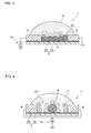
- a gas sensor according to the present invention is denoted by 1, and the gas sensor 1 is configured so as to be able to detect a gas, for example, such as CO 2 and NH 3 , as a target of detection.
- the gas sensor 1 includes a source electrode 3 and a drain electrode 4 in band shapes on a substrate 2 formed into a plate shape, and a carbon nanotube 8 is provided between the source electrode 3 and the drain electrode 4.
- the source electrode 3 and the drain electrode 4 are formed from, for example, a Ti/Au material or a Cr/Au material, and disposed substantially rectilinearly with respective longitudinal directions being aligned with each other, so that a gap of approximately 1 ⁇ m is formed between an end portion of the source electrode 3 and an end portion of the drain electrode 4 that face each other.
- the carbon nanotube 8 has one end side electrically connected to the end portion of the source electrode 3 and the other end side electrically connected to the end portion of the drain electrode 4, and is disposed so as to be positioned to form a straight line with the source electrode 3 and the drain electrode 4.
- the carbon nanotube 8 since the carbon nanotube 8 has a configuration in which a six-membered ring structure is rolled into a cylindrical shape in carbon, and has a large specific surface area, the carbon nanotube 8 correspondingly has a large contact surface to be in contact with an ionic liquid IL that will be described later, and also include excellent conductivity.
- the substrate 2 is provided with a gate electrode 7 formed from, for example, a Ti/Au material and a Cu/Au material, the ionic liquid IL is placed so as to be in contact with the gate electrode 7, and the carbon nanotube 8 is configured to be able to be contained in the ionic liquid IL.
- the gate electrode 7 is formed by a first gate electrode portion 5 and a second gate electrode portion 6 that are formed into the same shape and size, and the carbon nanotube 8, the source electrode 3 and the drain electrode 4 can be disposed in a gap G1 between the first gate electrode portion 5 and the second gate electrode portion 6.
- the first gate electrode portion 5 and the second gate electrode portion 6 are formed into semi-circular shapes, a straight line portion 5a of the first gate electrode portion 5 and a straight line portion 6a of the second gate electrode portion 6 are disposed in parallel with each other with the predetermined gap G1 therebetween.
- the carbon nanotube 8 In the gap G1 between these straight line portions 5a and 6a, the carbon nanotube 8, the source electrode 3 and the drain electrode 4 are disposed rectilinearly with respective longitudinal directions being aligned with one another.
- the ionic liquid IL is placed in a semi-spherical shape over the first gate electrode portion 5, the second gate electrode portion 6, the source electrode 3 and the drain electrode 4 in such a manner as to cover the entire carbon nanotube 8, and is configured to be able to function as a gate insulating layer.
- the ionic liquid IL is configured so that a semi-spherical liquid surface is exposed to outside air, and can contain the carbon nanotube 8 that is located in a central portion of the first gate electrode portion 5, the second gate electrode portion 6, the source electrode 3 and the drain electrode 4.
- the ionic liquid IL as a gas absorbing liquid is formed from, for example, [EMIM] [BF 4 ] (1-ethyl-3-methylimidazolium Tetrafluoroborate), [BMIM] [BF 4 ] (1-Butyl-3-methylimidazolium Tetrafluoroborate), [BMIM] [PF 6 ] (1-Butyl-3-methylimidazolium Hexafluorophosphate), or [OMIM][Br] (1-n-octyl-3-methylimidazolium bromide), besides the above, [Hmpy] [Tf 2 N], [HMIM] [Tf 2 N], [BMIM] [Tf 2 N], [C 6 H 4 F 9 min] [Tf 2 N], [AMIM] [BF 4 ], [Pabim] [BF 4 ], [Am-im] [DCA], [Am-im] [BF 4 ], [BMIM] [BF 4 ] + PVDF, [C 3 NH 2 mim] [EMI
- PEI polyethyleneimine
- the amino group of PEI transfers electric charges to the carbon nanotube 8, and can reduce the resistance value of the carbon nanotube 8.
- PEI reacts with CO 2 and H 2 O when the ionic liquid IL absorbs a gas, and the amino group of PEI decreases.
- the amino group of PEI in the ionic liquid IL decreases when the ionic liquid IL absorbs outside air with a high CO 2 content, as a result of which, the resistance value of the carbon nanotube 8 can increase, and an electric state of the carbon nanotube 8 can change in accordance with the CO 2 content in the outside air.
- the gas absorbing liquid IL is applied as the gas absorbing liquid
- various other gas absorbing liquids such as hydroxide aqueous solutions of an alkali metal and an alkaline earth metal may be applied.
- hydroxide aqueous solutions of an alkali metal and an alkaline earth metal are used as the gas absorbing liquid, the gas absorbing liquids can absorb CO 2 , and therefore, the gas sensor the detection target of which is CO 2 can be realized.
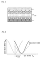
- the substrate 2 on which the ionic liquid IL is placed has a configuration in which a silicon oxide film 11 is formed on a silicon substrate 10, and has a configuration in which the source electrode 3, the drain electrode 4, the first gate electrode portion 5 and the second gate electrode portion 6 are provided on the silicon oxide film 11.
- the carbon nanotube 8 is configured so as to have one end side covered with the source electrode 3 and the other end side covered with the drain electrode 4, and to be capable of being electrically connected to the source electrode 3 and the drain electrode 4.
- the carbon nanotube 8 can have both the ends reliably fixed to the substrate 2 by having both the ends covered with the source electrode 3 and the drain electrode 4, and therefore, can keep an electric connection state to the source electrode 3 and the drain electrode 4 as it is without being removed from the substrate 2 when the ionic liquid IL is dropped.
- the carbon nanotube 8 as above has a diameter of approximately 1 to 10 nm, and is formed by growing in a straight line shape along the silicon oxide film 11 from a catalyst portion 12 provided on the silicon oxide film 11.
- the catalyst portion 12 is formed from a material prepared by, for example, mixing Co and silica at a predetermined ratio, and is covered with the drain electrode 4 together with the other end of the carbon nanotube 8.
- the gas sensor 1 like this is configured so that a source-drain current is supplied to the drain electrode 4 from the source electrode 3 by a power supply 13 as shown in Figure 3 , and as shown in Figure 4 , a gate voltage can be applied to the first gate electrode portion 5 and the second gate electrode portion 6 by a power supply 15.
- anions in the ionic liquid IL gather on the side peripheral surface of the carbon nanotube 8
- cations in the ionic liquid IL gather on the first gate electrode portion 5
- an electric double layer is formed in the ionic liquid IL as shown in Figure 5
- the ionic liquid IL can be a gate insulating layer.
- a gate voltage Vg is applied to the first gate electrode portion 5 and the second gate electrode portion 6, and a source-drain voltage V sd is applied between the source electrode 3 and the drain electrode 4, whereby an extremely thin gate insulating layer is formed in the ionic liquid IL, a source-drain current I sd flows in the carbon nanotube 8, and the gas sensor can operate as a transistor.
- the state of the gate insulating layer in the ionic liquid IL can be changed in accordance with the absorption amount of the gas, and source-drain current/gate voltage characteristics also can change in accordance with the change of the state of the gate insulating layer.
- the gas sensor 1 such the change of the source-drain current/gate voltage characteristics is measured, and the gas that is a target of detection can be detected based on the change of the source-drain current/gate voltage characteristics. Further, with the gas sensor 1, the change amount of the source-drain current/gate voltage characteristics is measured, and when the change amount is large, it is indicated that a gas concentration in the gas (hereinafter, also simply called outside air) around the ionic liquid IL is high, whereas when the change amount is small, it is indicated that the gas concentration in the outside air is low, so that the gas concentration in the outside air can be estimated.
- a gas concentration in the gas hereinafter, also simply called outside air
- a waveform close to a substantially V-shape can be obtained as the relationship between the source drain current I sd and the gate voltage V g when the gas that is a target of detection is not contained in the gas around the ionic liquid IL, as shown in Figure 6 .
- the gate voltage Vg in the gas sensor 1 can shift by a shift voltage V shift .
- the shift voltage V shift can increase in proportion thereto.
- the gas sensor 1 of the present invention detection of the gas contained in outside air and estimation of the content of the gas are enabled based on a change of the source-drain current I sd , and the change of the gate voltage Vg that occurs due to the change of the source-drain current I sd .
- the gas sensor 1 which is provided with the gate electrode 7, applies the gate voltage Vg to the first gate electrode portion 5 and the second gate electrode portion 6 that configure the gate electrode 7, forms the electric double layer on the surface of the carbon nanotube 8 in the ionic liquid IL, and measures the change of the source-drain current I sd which flows in the carbon nanotube 8 as a result of the state of the electric double layer changing by the ionic liquid IL absorbing a gas.
- the present invention is not limited to this, and may be a gas sensor that is not provided with the gate electrode 7, and simply measures the change of the source-drain current I sd that flows in the carbon nanotube 8 between the source electrode 3 and the drain electrode 4 by the ionic liquid IL absorbing a gas.
- a substrate 2 in which a silicon oxide film 11 is formed on a silicon substrate 10 is prepared first of all, and a resist layer of a predetermined pattern is formed on the silicon oxide film 11.
- a catalyst layer 19 is formed on the resist layer 18 on the substrate 2 by spin coating, and the catalyst layer 19 is also formed on the silicon oxide film 11 that is exposed in an opening 18a formed in the resist layer 18.
- a catalyst material formed by mixing, for example, Co and fumed silica at a ratio of 1:10, or the like is used for the catalyst layer 19 is removed by lift-off, only the catalyst layer 19 that is formed in the opening 18a is left, and the catalyst portion 12 of 3 to 7 [ ⁇ m] is formed in rectangular shape.
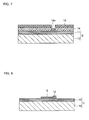
- a carbon is grown from the catalyst portion 12 by a chemical vapor deposition method (CVD), and the carbon nanotube 8 that extends rectilinearly from the catalyst portion 12 is formed on the silicon oxide film 11 as shown in Figure 8 .
- CVD chemical vapor deposition method
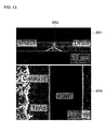
- the resist layer is patterned by exposure, and as shown in Figure 9 , after a resist layer 21 is left in central regions of the carbon nanotube 8 that are exposed in the ionic liquid IL, for example, an electrode layer 22 formed from Ti/Au (5/50) is formed on the entire surface.
- the resist layer 21 is removed by lift-off and the electrode layer 22 is patterned, whereby the central regions of the carbon nanotube 8 is exposed, and the source electrode 3, the drain electrode 4, and further the first gate electrode portion 5 and the second gate electrode portion 6 which are not illustrated are formed on the silicon oxide film 11 as shown in Figure 10 .
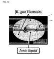
- the ionic liquid IL is dropped onto the substrate 2 in such a manner as to cover the entire carbon nanotube 8 that are exposed between the source electrode 3 and the drain electrode 4, whereby as shown in Figure 12 , the gas sensor 1 can be produced, in which the ionic liquid IL (described as "Ionic Liquid” in the drawing) is in contact with the source electrode 3 (described as “Source” in the drawing), the drain electrode 4 (described as “Drain” in the drawing) and the gate electrode 7 (the first gate electrode portion 5 and the second gate electrode portion 6, described as "IL-gate Electrodes” in the drawing).
- the ionic liquid IL described as "Ionic Liquid” in the drawing
- the source electrode 3, the drain electrode 4, and the gate electrode 7 were respectively formed from Ti/Au (film thickness 5 [nm]/50 [nm])
- the carbon nanotube 8 was formed from the catalyst portion 12 formed by mixing Co and fumed silica at 1:10
- the gas sensor 1 in which the gap between the source electrode 3 and the drain electrode 4 was set at 1 [ ⁇ m] and the resistance value of the carbon nanotube 8 was set at 5 to 100 [k ⁇ ] was produced.
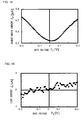
- Figure 14 shows the relation of the source-drain current I sd and the gate voltage Vg when the source-drain voltage V sd between the source electrode 3 and the drain electrode 4 of the gas sensor 1 was set at 10 [mV], and the gate voltage Vg that was applied to the gate electrode 7 was increased from -0.3 [V] to 0.3 [V] at 5 [mV/sec]. From Figure 14 , it was confirmed that in the gas sensor 1, a waveform close to a gentle V-shape is obtained when the gas that is a target of detection is not contained in outside air.
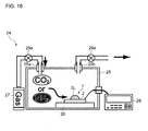
- a verification test was performed concerning whether or not the gas that is a target of detection is detectable in the gas sensor 1.
- the gas that is a target of detection was supplied into a chamber 25 of 300 ⁇ 300 ⁇ 100 [mm 3 ] through a supply port 25a from a gas storage section 27 via a valve 29a, and the gas was discharged to an outside of the chamber 25 from a discharge port 25b via a valve 29b.
- the gas sensor 1 was placed on a base 26 in the chamber 25, and a measuring device 28 provided outside the chamber 25 and the gas sensor 1 in the chamber 25 were connected while a sealed state of the chamber 25 is kept.
- the gas sensor 1 using [EMIM] [BF 4 ] as the ionic liquid IL was installed in the chamber 25 first of all, after which, the inside of the chamber 25 was filled with air (Air) that does not contain the gas that is a target to be detected, and the relation between the source-drain current I sd and the gate voltage Vg in the gas sensor 1 at this time was examined. Thereafter, CO 2 was supplied into the chamber 25, the inside of the chamber 25 was filled with a mixture gas prepared by mixing 12[%] of CO 2 into outside air (Air), and the relation of the source-drain current I sd and the gate voltage Vg in the gas sensor 1 was also examined after stabilization.
- Air air
- CO 2 was supplied into the chamber 25
- the inside of the chamber 25 was filled with a mixture gas prepared by mixing 12[%] of CO 2 into outside air (Air)
- the relation of the source-drain current I sd and the gate voltage Vg in the gas sensor 1 was also examined after stabilization.
- the gas sensor 1 absorbs CO 2 as a target of detection, as a result of which, the state of the gate insulating layer that is formed in the ionic liquid IL changes, the source-drain current I sd changes, and the shift voltage V shift is generated.
- the gas sensor 1 of the present invention can detect CO 2 in the outside air around the ionic liquid IL, by measuring the change of the source-drain current I sd .
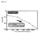
- the gas sensor 1 using ionic liquid IL prepared by mixing PEI (branched, M. W. 10,000) into [EMIM] [BF 4 ] as the ionic liquid IL, and using a metallic carbon nanotube as the carbon nanotube 8 was prepared.
- PEI branched, M. W. 10,000
- EMIM [BF 4 ]
- metallic carbon nanotube as the carbon nanotube 8 was prepared.
- an I-V characteristic was measured after the carbon nanotube 8 was produced, and determination was performed from the shape of the curve of the I-V characteristic.
- the inside of the chamber 25 was filled with air (Air), and the relation of the source-drain current I sd and the gate voltage Vg in the gas sensor 1 at this time was examined.
- CO 2 was supplied into the chamber 25, the inside of the chamber 25 was filled with a mixture gas prepared by mixing CO 2 into the air (Air) by 24[%], and after stabilization, the relation of the source-drain current I sd and the gate voltage Vg in the gas sensor 1 was also examined.
- the gas sensor 1 using the ionic liquid IL prepared by mixing PEI (branched, M. W. 10,000) into [EMIM] [BF 4 ] that is the same as described above as the ionic liquid IL, and using a semiconductor carbon nanotube as the carbon nanotube 8 was prepared.
- the inside of the chamber 25 was filled with air (Air), and the relation of the source-drain current I sd and the gate voltage Vg in the gas sensor 1 at this time was examined.
- CO 2 was supplied into the chamber 25, the inside of the chamber 25 was filled with a mixture gas in which CO 2 was mixed into the air (Air) by 25[%], and after stabilization, the relation between the source-drain current I sd and the gate voltage Vg in the gas sensor 1 was also examined.
- the gas sensor 1 is configured such that the carbon nanotube 8 is provided between the source electrode 3 and the drain electrode 4 on the substrate 2, and the carbon nanotube 8 is covered with the ionic liquid IL.
- the carbon nanotube 8 having a large number of holes is located in the ionic liquid IL, and thereby the negative electric charges in the ionic liquid IL gather on the surface of the carbon nanotube 8.
- the ionic liquid IL absorbs a gas that is a target of detection in the gas sensor 1
- the state of the negative electric charges that gather on the surface of the carbon nanotube 8 in the ionic liquid IL changes, and with this change, the source-drain current I sd that flows in the carbon nanotube 8 also changes, whereby based on the tendency of the change of the source-drain current I sd , the gas in the outside air can be detected.
- the carbon nanotube 8 is provided between the source electrode 3 and the drain electrode 4 on the substrate 2, the ionic liquid IL to be the gate insulating layer is provided in contact with the carbon nanotube 8 and the gate electrode 7 on the substrate 2, and a gate voltage is applied to the ionic liquid IL via the gate electrode 7.
- the electric double layer having the gate insulating layer is formed in the ionic liquid IL that absorbs a gas, and the gas sensor 1 can operate as a transistor capable of measuring the source-drain current I sd that flows in the carbon nanotube 8.
- the state of the gate insulating layer in the ionic liquid IL changes when the ionic liquid IL absorbs the gas that is a target of detection, and the source-drain current I sd that flows in the carbon nanotube in the ionic liquid IL changes in response to the state of the gate insulating layer. Therefore, the change of the source-drain current I sd is measured, and the gas in the outside air can be detected based on the tendency of the change of the source-drain current I sd .
- a silicon oxide film with a film thickness of 150 to 200 [nm], for example, is used as a gate insulating layer between the silicon back gate and the carbon nanotube, and therefore, in order to operate the gas sensor as a transistor, a gate voltage of approximately 15 [V] at the maximum is needed.
- an extremely thin gate insulating layer of several nanometers is formed in the ionic liquid IL provided between the carbon nanotube 8 and the gate electrode 7 without using a silicon oxide film such as SiO 2 , whereby even if the gate voltage Vg of approximately 0.4 [V] is applied to the gate electrode 7, the gas sensor can operate as a transistor, and the gate voltage Vg can be more drastically reduced than in the conventional gas sensors.
- the gate insulating layer is formed in the ionic liquid IL itself that absorbs a gas, and the change of the state of the gate insulating layer of the ionic liquid IL, which occurs by absorption of the gas is directly reflected in the source-drain current that flows in the carbon nanotube 8, the gas detection sensitivity can be enhanced more than in the conventional gas sensors. Furthermore, since in the gas sensor 1, surface chemical modification does not have to be applied to the carbon nanotube itself as in the conventional gas sensors, and the ionic liquid IL can be simply provided to be in contact with the carbon nanotube 8 and the gate electrode 7, and therefore, the configuration can be simplified correspondingly.
- the source-drain current/gate voltage characteristics change in accordance with the gas concentration in the outside air, and therefore, by measuring the change amount of the source-drain current/gate voltage characteristics, to what extent the gas which is the target of detection is contained in the outside air also can be estimated based on the change amount.
- the carbon nanotube 8 by providing the carbon nanotube 8 between the source electrode 3 and the drain electrode 4 in the ionic liquid IL, the change of the state of the electric charges in the ionic liquid IL, which occurs by absorption of a gas is directly reflected in the source-drain current I sd that flows in the carbon nanotube 8, and therefore, the gas detection sensitivity can be enhanced more than in the conventional gas sensors. Further, since the carbon nanotube 8 can be simply provided to be disposed in the ionic liquid IL, the configuration that chemically modifies the surface of the carbon nanotube with a plurality of polymers as in the conventional gas sensors is not necessary, and the configuration can be simplified correspondingly.
- the electric double layer including the gate insulating layer is formed in the ionic liquid IL, and the change of the state of the gate insulating layer in the ionic liquid IL, which occurs by absorption of a gas is directly reflected in the source-drain current I sd that flows in the carbon nanotube 8, and therefore, the gas detection sensitivity can be enhanced more than in the conventional gas sensors.
- the ionic liquid IL can be simply provided on the substrate 2 to be in contact with the carbon nanotube 8 and the gate electrode 7, the configuration that chemically modifies the surface of the carbon nanotube with a plurality of polymers as in the conventional gas sensors is not needed, and the configuration can be simplified correspondingly.
- the present invention is not limited to the present embodiment, and can be carried out by being variously modified within the range of the gist of the present invention.
- the gas sensor 1 is described, in which the ionic liquid IL is provided to be placed not only on the source electrode 3 and the drain electrode 4, but also on the first gate electrode portion 5 and the second gate electrode portion 6, but the present invention is not limited to this.
- a gas sensor 31 may be applied, in which an ionic liquid IL1 is provided in only a region G2 surrounded by the source electrode 3, the drain electrode 4, the first gate electrode portion 5, and the second gate electrode portion 6 without covering the top surfaces of the source electrode 3, the drain electrode 4, the gate electrode portion 5 and the second gate electrode portion 6, as in Figure 22 showing the configuration by assigning the components corresponding to those in Figure 1 with the same reference signs, Figure 23 showing a sectional configuration of a C-C' portion of Figure 22 , and Figure 24 showing a sectional configuration of a D-D' portion of Figure 22 .
- the ionic liquid IL1 is disposed in the region G2 surrounded by the source electrode 3, the drain electrode 4, the first gate electrode portion 5 and the second gate electrode portion 6 to be in contact with respective side surfaces of the source electrode 3, the drain electrode 4, the first gate electrode portion 5 and the second gate electrode portion 6, miniaturization can be achieved by reducing the amount of the ionic liquid IL1, and the ionic liquid IL1 can be provided on the substrate 2 stably by action of surface tension as well.
- an electric double layer including a gate insulating layer of several nanometers is formed in the ionic liquid IL1 when a gate voltage is applied to the ionic liquid IL1 via the gate electrode 7 similarly to the aforementioned embodiment.
- the ionic liquid IL1 can be reduced to the volume with which the gate insulating layer of approximately several nanometers of the electric double layer can be formed.
- a gas sensor 41 may be applied, which has a configuration in which a liquid surface of the ionic liquid IL formed in a curved shape is covered with a coating film 42 capable of permeating outside air such as parylene, as in Figure 25 showing the configuration by assigning the components corresponding to those in Figure 3 with the same reference signs.
- a coating film 42 capable of permeating outside air such as parylene
- the gas sensor 41 can be produced by depositing a coating material capable of permeating outside air such as parylene on the ionic liquid IL by, for example, a CVD (Chemical Vapor Deposition) method, after dropping the ionic liquid IL, and forming the coating film 42 directly onto the ionic liquid IL. Further, the gas sensor 41 also can be produced by forming the coating film 42 on the substrate 2 in advance by a coating material capable of permeating outside air such as parylene, and thereafter injecting the ionic liquid IL into the coating film 42 and sealing the ionic liquid IL.
- a coating material capable of permeating outside air such as parylene
- the ionic liquid IL can be held on the substrate 2 stably by the coating film 42, the substrate 2 can be installed on the ceiling in a room with the ionic liquid IL facing down, for example, and the substrate can be installed with the ionic liquid IL facing in various directions in accordance with service conditions.
- a gas absorbing liquid can be isolated from outside air, and therefore, as the gas absorbing liquid, a volatile liquid such as water also can be used. Note that when water is used as the gas absorbing liquid, the water absorbs a gas, whereby in response to a change of the state of the electric charges in the water, the source-drain current I sd that flows in the carbon nanotube 8 changes, and a similar effect to the embodiment described above can be obtained.
- a gas sensor 51 may be applied, which is configured such that a frame body 52 covering the ionic liquid IL is provided on the substrate 2, and the ionic liquid IL is held on the substrate 2 by the frame body 52 as holding means.
- the frame body 52 is disposed on the substrate 2 in such a manner as to cover the carbon nanotube 8 (not illustrated) between the source electrode 3 and the drain electrode 4 on the substrate 2, to cover parts of the source electrode 3, the drain electrode 4 and the gate electrode 7 that are disposed around the carbon nanotube 8, and to be able to hold the ionic liquid IL in an internal space.
- the frame body 52 forms the internal space by, for example, a quadrilateral wall portion 52a that holds back the ionic liquid IL, and a plate-shaped top plate portion 52b that is disposed to cover the wall portion 52a, and a plurality of microscopic through-holes 53 that allow the internal space and an outside to communicate with each other are provided by being drilled in the top plate portion 52b.
- the frame body 52 has a bottom surface portion closed by being installed on the substrate 2, has the internal space communicating with the outside through only the through-holes 53, and can hold the ionic liquid IL in the internal space by the ionic liquid IL being injected into the internal space from the through-holes 53.
- the frame body 52 is configured to be able to hold the ionic liquid IL reliably, since the surface tension of the ionic liquid IL acts in the through-hole 53 because the through-hole 53 is microscopic, and the ionic liquid IL injected into the internal space hardly flows outside from the through-hole 53.
- the ionic liquid IL covers the carbon nanotube in the internal space of the frame body 52, and is also in contact with the first gate electrode portion 5 and the second gate electrode portion 6 (not illustrated) of the gate electrode 7.
- the electric double layer including the gate insulating layer is formed in the ionic liquid IL when the gate voltage is applied to the ionic liquid IL from the gate electrode 7, and a similar effect to the above described embodiment can be provided.
- a configuration may be adopted, in which the substrate 2 provided with the carbon nanotube 8, the gate electrode 7 and the like is installed in a box-shaped storage portion in which the ionic liquid IL is stored, and the substrate 2 is provided in the ionic liquid IL.
- Such gas sensors with various configurations each with the disposition relation of the substrate 2 and the ionic liquid IL appropriately changed may be applied in accordance with service conditions.
Landscapes
- Chemical & Material Sciences (AREA)
- Health & Medical Sciences (AREA)
- Life Sciences & Earth Sciences (AREA)
- Engineering & Computer Science (AREA)
- Biochemistry (AREA)
- General Health & Medical Sciences (AREA)
- Pathology (AREA)
- Immunology (AREA)
- Physics & Mathematics (AREA)
- Analytical Chemistry (AREA)
- General Physics & Mathematics (AREA)
- Electrochemistry (AREA)
- Chemical Kinetics & Catalysis (AREA)
- Molecular Biology (AREA)
- Microelectronics & Electronic Packaging (AREA)
- Combustion & Propulsion (AREA)
- Food Science & Technology (AREA)
- Medicinal Chemistry (AREA)
- Nanotechnology (AREA)
- Investigating Or Analyzing Materials By The Use Of Electric Means (AREA)
Applications Claiming Priority (2)
| Application Number | Priority Date | Filing Date | Title |
|---|---|---|---|
| JP2012004963 | 2012-01-13 | ||
| PCT/JP2012/083879 WO2013105449A1 (ja) | 2012-01-13 | 2012-12-27 | ガスセンサ |
Publications (3)
| Publication Number | Publication Date |
|---|---|
| EP2803984A1 true EP2803984A1 (de) | 2014-11-19 |
| EP2803984A4 EP2803984A4 (de) | 2015-08-12 |
| EP2803984B1 EP2803984B1 (de) | 2017-09-13 |
Family
ID=48781405
Family Applications (1)
| Application Number | Title | Priority Date | Filing Date |
|---|---|---|---|
| EP12864780.7A Not-in-force EP2803984B1 (de) | 2012-01-13 | 2012-12-27 | Gassensor |
Country Status (6)
| Country | Link |
|---|---|
| US (1) | US9250210B2 (de) |
| EP (1) | EP2803984B1 (de) |
| JP (1) | JP5822282B2 (de) |
| KR (1) | KR20140089432A (de) |
| CN (1) | CN103988071A (de) |
| WO (1) | WO2013105449A1 (de) |
Families Citing this family (26)
| Publication number | Priority date | Publication date | Assignee | Title |
|---|---|---|---|---|
| US20150323482A1 (en) * | 2012-12-28 | 2015-11-12 | The University Of Tokyo | Gas sensor and gas sensor structural body |
| EP3041785A1 (de) | 2013-09-06 | 2016-07-13 | Massachusetts Institute of Technology | Vorrichtungen und verfahren mit einem vorkonzentratormaterial zum nachweis von analyten |
| EP3041597B1 (de) | 2013-09-06 | 2022-11-02 | Massachusetts Institute of Technology | Filtermaterialien mit funktionalisierter cellulose |
| GB2523173A (en) * | 2014-02-17 | 2015-08-19 | Nokia Technologies Oy | An apparatus and associated methods |
| WO2017168570A1 (ja) * | 2016-03-29 | 2017-10-05 | 三菱電機株式会社 | 空調機 |
| JP6661080B2 (ja) * | 2016-04-18 | 2020-03-11 | 株式会社東海理化電機製作所 | バイオセンサ |
| IL252498A0 (en) * | 2017-05-24 | 2017-07-31 | Technion Res & Dev Foundation | Carbon dioxide detectors containing polymeric ionic liquid |
| CN107219287B (zh) * | 2017-06-28 | 2023-11-17 | 汉威科技集团股份有限公司 | 离子液体电化学气体传感器 |
| US12196636B2 (en) | 2019-03-27 | 2025-01-14 | Lyten, Inc. | Sensors incorporated into airborne vehicle components to detect physical characteristic changes |
| US11592279B2 (en) | 2019-03-27 | 2023-02-28 | Lyten, Inc. | Sensors incorporated into elastomeric materials to detect environmentally-caused physical characteristic changes |
| US11719582B2 (en) | 2019-03-27 | 2023-08-08 | Lyten, Inc. | Sensors incorporated into tire plies to detect reversible deformation and/or temperature changes |
| US11656070B2 (en) | 2019-03-27 | 2023-05-23 | Lyten, Inc. | Systems for detecting physical property changes in an elastomeric material |
| US12317466B2 (en) | 2019-03-27 | 2025-05-27 | Lyten, Inc. | Frequency selective metamaterial for protective enclosures |
| US11555748B2 (en) | 2019-03-27 | 2023-01-17 | Lyten, Inc. | Sensors incorporated into tire plies to detect reversible deformation and/or temperature changes |
| US12265058B2 (en) | 2019-03-27 | 2025-04-01 | Lyten, Inc. | Sensors incorporated into adhesive material |
| US11555761B1 (en) | 2019-03-27 | 2023-01-17 | Lyten, Inc. | Sensors incorporated into elastomeric components to detect physical characteristic changes |
| US11585731B2 (en) | 2019-03-27 | 2023-02-21 | Lyten, Inc. | Sensors incorporated into semi-rigid structural members to detect physical characteristic changes |
| US12339272B2 (en) | 2019-03-27 | 2025-06-24 | Lyten, Inc. | Sensors incorporated into building materials to detect physical characteristic changes |
| US12270785B2 (en) | 2019-03-27 | 2025-04-08 | Lyten, Inc. | Water droplet sensing systems and methods |
| US11965803B2 (en) | 2019-03-27 | 2024-04-23 | Lyten, Inc. | Field deployable resonant sensors |
| US12313570B2 (en) | 2019-03-27 | 2025-05-27 | Lyten, Inc. | Leaky coaxial resonant sensor systems and methods |
| CN110596222A (zh) * | 2019-09-16 | 2019-12-20 | 北京大学 | 一种碳纳米管场效应晶体管型传感器及其制备方法 |
| EP4491573A3 (de) * | 2020-02-20 | 2025-03-19 | Lyten, Inc. | Analyterfassungsvorrichtung |
| JP2022169933A (ja) * | 2021-04-28 | 2022-11-10 | 東レ株式会社 | ガスセンサー素子およびガスセンサー |
| KR102652552B1 (ko) * | 2022-02-24 | 2024-03-29 | 단국대학교 산학협력단 | 산화갈륨을 이용한 가스 센서 |
| US20240275608A1 (en) | 2023-02-15 | 2024-08-15 | Lyten, Inc. | Method to learn precise sensing fingerprints based on machine learning integration |
Family Cites Families (16)
| Publication number | Priority date | Publication date | Assignee | Title |
|---|---|---|---|---|
| JPS60125558A (ja) * | 1983-12-09 | 1985-07-04 | Kuraray Co Ltd | ガスセンサ |
| CA1251514A (en) * | 1985-02-20 | 1989-03-21 | Tadashi Sakai | Ion selective field effect transistor sensor |
| JPH0679009B2 (ja) * | 1985-11-22 | 1994-10-05 | 株式会社東芝 | 化学センサ |
| JP3167022B2 (ja) * | 1988-11-18 | 2001-05-14 | 新電元工業株式会社 | ガスセンサ |
| JPH03237350A (ja) * | 1990-02-14 | 1991-10-23 | Terumo Corp | pHセンサーおよびその製造方法 |
| US8154093B2 (en) * | 2002-01-16 | 2012-04-10 | Nanomix, Inc. | Nano-electronic sensors for chemical and biological analytes, including capacitance and bio-membrane devices |
| US20070048181A1 (en) * | 2002-09-05 | 2007-03-01 | Chang Daniel M | Carbon dioxide nanosensor, and respiratory CO2 monitors |
| JP2004085392A (ja) * | 2002-08-27 | 2004-03-18 | Fujitsu Ltd | 炭素元素線状構造体を用いた電界効果トランジスタ化学センサー |
| US6949931B2 (en) * | 2002-11-26 | 2005-09-27 | Honeywell International Inc. | Nanotube sensor |
| EP1664724A4 (de) * | 2003-09-12 | 2007-05-02 | Nanomix Inc | Nanoelektronischer kohlendioxidsensor |
| JP4891550B2 (ja) * | 2005-02-10 | 2012-03-07 | 独立行政法人科学技術振興機構 | n型トランジスタ、n型トランジスタセンサ及びn型トランジスタ用チャネルの製造方法 |
| JP2010192599A (ja) | 2009-02-17 | 2010-09-02 | Olympus Corp | カーボンナノ材料を用いた電界効果トランジスタにおける絶縁膜成膜方法及びカーボンナノ材料を用いた電界効果トランジスタ |
| JP5369755B2 (ja) | 2009-02-25 | 2013-12-18 | 株式会社豊田中央研究所 | ガスセンサ |
| JP2010203838A (ja) | 2009-03-02 | 2010-09-16 | Sonac Kk | 光導波路型センサ |
| JP2010261793A (ja) | 2009-05-01 | 2010-11-18 | Kurabo Ind Ltd | 液体中の溶存物質含有量測定方法及び測定装置、並びに、エッチング液再生システム |
| WO2011155179A1 (ja) | 2010-06-10 | 2011-12-15 | コニカミノルタホールディングス株式会社 | 分析素子チップ |
-
2012
- 2012-12-27 EP EP12864780.7A patent/EP2803984B1/de not_active Not-in-force
- 2012-12-27 US US14/366,912 patent/US9250210B2/en not_active Expired - Fee Related
- 2012-12-27 WO PCT/JP2012/083879 patent/WO2013105449A1/ja not_active Ceased
- 2012-12-27 CN CN201280060963.XA patent/CN103988071A/zh active Pending
- 2012-12-27 JP JP2013553247A patent/JP5822282B2/ja not_active Expired - Fee Related
- 2012-12-27 KR KR1020147015752A patent/KR20140089432A/ko not_active Ceased
Also Published As
| Publication number | Publication date |
|---|---|
| CN103988071A (zh) | 2014-08-13 |
| EP2803984A4 (de) | 2015-08-12 |
| US20140346042A1 (en) | 2014-11-27 |
| JPWO2013105449A1 (ja) | 2015-05-11 |
| EP2803984B1 (de) | 2017-09-13 |
| WO2013105449A1 (ja) | 2013-07-18 |
| JP5822282B2 (ja) | 2015-11-24 |
| KR20140089432A (ko) | 2014-07-14 |
| US9250210B2 (en) | 2016-02-02 |
Similar Documents
| Publication | Publication Date | Title |
|---|---|---|
| US9250210B2 (en) | Gas sensor | |
| EP2940462A1 (de) | Gassensor und strukturkörper für den gassensor | |
| Qin et al. | Microfabricated electrochemical pH and free chlorine sensors for water quality monitoring: Recent advances and research challenges | |
| Hong et al. | Highly selective ZnO gas sensor based on MOSFET having a horizontal floating-gate | |
| Ko et al. | Recovery improvement for large-area tungsten diselenide gas sensors | |
| EP2372355A2 (de) | Amorphe Dünnschicht zum Messen | |
| US10191008B2 (en) | Gas sensor with solid electrolyte having water vapor diffusion barrier coating | |
| Krüger et al. | Electrochemical carbon nanotube field-effect transistor | |
| Postica et al. | Improved long‐term stability and reduced humidity effect in gas sensing: SiO2 ultra‐thin layered ZnO columnar films | |
| US9018684B2 (en) | Chemical sensing and/or measuring devices and methods | |
| Deb et al. | Achieving room-temperature ppb-level H2S detection in a Au-SnO2 sensor with low voltage enhancement effect | |
| Rathi et al. | Ruthenium-decorated tungsten disulfide quantum dots for a CO2 gas sensor | |
| Zhou et al. | High performance gas sensors with dual response based on organic ambipolar transistors | |
| Ranjan et al. | AlGaN/GaN HEMT-based high-sensitive NO2 gas sensors | |
| CN107430086A (zh) | 气体传感器以及传感器装置 | |
| Mubeen et al. | Gas Sensing Mechanism of Gold Nanoparticles Decorated Single‐Walled Carbon Nanotubes | |
| Lee et al. | Selective and rapid room temperature detection of H2S using gold nanoparticle chain arrays | |
| US8431001B2 (en) | Ion sensor for measuring ion concentration of a solution | |
| WO2006109878A8 (en) | Light-emitting element, light-emitting device, and vapor deposition apparatus | |
| Kiga et al. | CNT-FET gas sensor using a functionalized ionic liquid as gate | |
| Chandresh et al. | Metal‐Organic Framework Thin Films Grown on Functionalized Graphene as Solid‐State Ion‐Gated FETs | |
| JP6536592B2 (ja) | ガスセンサ及びセンサ装置 | |
| CN109411604B (zh) | 传感器及其制备方法、阵列基板、显示面板、显示装置 | |
| Bae et al. | Field-effect transistors based on organic and carbon-based materials for chemical and biological sensors | |
| KR20140022520A (ko) | 표면 개질된 탄소나노구조체를 이용한 이온 농도 측정용 센서 및 그 제조방법 |
Legal Events
| Date | Code | Title | Description |
|---|---|---|---|
| PUAI | Public reference made under article 153(3) epc to a published international application that has entered the european phase |
Free format text: ORIGINAL CODE: 0009012 |
|
| 17P | Request for examination filed |
Effective date: 20140624 |
|
| AK | Designated contracting states |
Kind code of ref document: A1 Designated state(s): AL AT BE BG CH CY CZ DE DK EE ES FI FR GB GR HR HU IE IS IT LI LT LU LV MC MK MT NL NO PL PT RO RS SE SI SK SM TR |
|
| DAX | Request for extension of the european patent (deleted) | ||
| RA4 | Supplementary search report drawn up and despatched (corrected) |
Effective date: 20150715 |
|
| RIC1 | Information provided on ipc code assigned before grant |
Ipc: G01N 33/00 20060101ALI20150709BHEP Ipc: H01L 29/786 20060101ALI20150709BHEP Ipc: H01L 51/05 20060101ALI20150709BHEP Ipc: H01L 51/00 20060101ALI20150709BHEP Ipc: G01N 27/00 20060101AFI20150709BHEP Ipc: G01N 27/414 20060101ALI20150709BHEP Ipc: H01L 51/30 20060101ALI20150709BHEP |
|
| GRAP | Despatch of communication of intention to grant a patent |
Free format text: ORIGINAL CODE: EPIDOSNIGR1 |
|
| STAA | Information on the status of an ep patent application or granted ep patent |
Free format text: STATUS: GRANT OF PATENT IS INTENDED |
|
| INTG | Intention to grant announced |
Effective date: 20170329 |
|
| GRAS | Grant fee paid |
Free format text: ORIGINAL CODE: EPIDOSNIGR3 |
|
| GRAA | (expected) grant |
Free format text: ORIGINAL CODE: 0009210 |
|
| STAA | Information on the status of an ep patent application or granted ep patent |
Free format text: STATUS: THE PATENT HAS BEEN GRANTED |
|
| AK | Designated contracting states |
Kind code of ref document: B1 Designated state(s): AL AT BE BG CH CY CZ DE DK EE ES FI FR GB GR HR HU IE IS IT LI LT LU LV MC MK MT NL NO PL PT RO RS SE SI SK SM TR |
|
| REG | Reference to a national code |
Ref country code: GB Ref legal event code: FG4D |
|
| REG | Reference to a national code |
Ref country code: CH Ref legal event code: EP |
|
| REG | Reference to a national code |
Ref country code: IE Ref legal event code: FG4D |
|
| REG | Reference to a national code |
Ref country code: AT Ref legal event code: REF Ref document number: 928644 Country of ref document: AT Kind code of ref document: T Effective date: 20171015 |
|
| REG | Reference to a national code |
Ref country code: DE Ref legal event code: R096 Ref document number: 602012037445 Country of ref document: DE |
|
| REG | Reference to a national code |
Ref country code: NL Ref legal event code: MP Effective date: 20170913 |
|
| REG | Reference to a national code |
Ref country code: LT Ref legal event code: MG4D |
|
| PG25 | Lapsed in a contracting state [announced via postgrant information from national office to epo] |
Ref country code: NO Free format text: LAPSE BECAUSE OF FAILURE TO SUBMIT A TRANSLATION OF THE DESCRIPTION OR TO PAY THE FEE WITHIN THE PRESCRIBED TIME-LIMIT Effective date: 20171213 Ref country code: HR Free format text: LAPSE BECAUSE OF FAILURE TO SUBMIT A TRANSLATION OF THE DESCRIPTION OR TO PAY THE FEE WITHIN THE PRESCRIBED TIME-LIMIT Effective date: 20170913 Ref country code: SE Free format text: LAPSE BECAUSE OF FAILURE TO SUBMIT A TRANSLATION OF THE DESCRIPTION OR TO PAY THE FEE WITHIN THE PRESCRIBED TIME-LIMIT Effective date: 20170913 Ref country code: LT Free format text: LAPSE BECAUSE OF FAILURE TO SUBMIT A TRANSLATION OF THE DESCRIPTION OR TO PAY THE FEE WITHIN THE PRESCRIBED TIME-LIMIT Effective date: 20170913 Ref country code: FI Free format text: LAPSE BECAUSE OF FAILURE TO SUBMIT A TRANSLATION OF THE DESCRIPTION OR TO PAY THE FEE WITHIN THE PRESCRIBED TIME-LIMIT Effective date: 20170913 |
|
| REG | Reference to a national code |
Ref country code: AT Ref legal event code: MK05 Ref document number: 928644 Country of ref document: AT Kind code of ref document: T Effective date: 20170913 |
|
| PG25 | Lapsed in a contracting state [announced via postgrant information from national office to epo] |
Ref country code: RS Free format text: LAPSE BECAUSE OF FAILURE TO SUBMIT A TRANSLATION OF THE DESCRIPTION OR TO PAY THE FEE WITHIN THE PRESCRIBED TIME-LIMIT Effective date: 20170913 Ref country code: GR Free format text: LAPSE BECAUSE OF FAILURE TO SUBMIT A TRANSLATION OF THE DESCRIPTION OR TO PAY THE FEE WITHIN THE PRESCRIBED TIME-LIMIT Effective date: 20171214 Ref country code: BG Free format text: LAPSE BECAUSE OF FAILURE TO SUBMIT A TRANSLATION OF THE DESCRIPTION OR TO PAY THE FEE WITHIN THE PRESCRIBED TIME-LIMIT Effective date: 20171213 Ref country code: LV Free format text: LAPSE BECAUSE OF FAILURE TO SUBMIT A TRANSLATION OF THE DESCRIPTION OR TO PAY THE FEE WITHIN THE PRESCRIBED TIME-LIMIT Effective date: 20170913 |
|
| PG25 | Lapsed in a contracting state [announced via postgrant information from national office to epo] |
Ref country code: NL Free format text: LAPSE BECAUSE OF FAILURE TO SUBMIT A TRANSLATION OF THE DESCRIPTION OR TO PAY THE FEE WITHIN THE PRESCRIBED TIME-LIMIT Effective date: 20170913 |
|
| PG25 | Lapsed in a contracting state [announced via postgrant information from national office to epo] |
Ref country code: CZ Free format text: LAPSE BECAUSE OF FAILURE TO SUBMIT A TRANSLATION OF THE DESCRIPTION OR TO PAY THE FEE WITHIN THE PRESCRIBED TIME-LIMIT Effective date: 20170913 Ref country code: PL Free format text: LAPSE BECAUSE OF FAILURE TO SUBMIT A TRANSLATION OF THE DESCRIPTION OR TO PAY THE FEE WITHIN THE PRESCRIBED TIME-LIMIT Effective date: 20170913 Ref country code: RO Free format text: LAPSE BECAUSE OF FAILURE TO SUBMIT A TRANSLATION OF THE DESCRIPTION OR TO PAY THE FEE WITHIN THE PRESCRIBED TIME-LIMIT Effective date: 20170913 |
|
| PG25 | Lapsed in a contracting state [announced via postgrant information from national office to epo] |
Ref country code: AT Free format text: LAPSE BECAUSE OF FAILURE TO SUBMIT A TRANSLATION OF THE DESCRIPTION OR TO PAY THE FEE WITHIN THE PRESCRIBED TIME-LIMIT Effective date: 20170913 Ref country code: IS Free format text: LAPSE BECAUSE OF FAILURE TO SUBMIT A TRANSLATION OF THE DESCRIPTION OR TO PAY THE FEE WITHIN THE PRESCRIBED TIME-LIMIT Effective date: 20180113 Ref country code: IT Free format text: LAPSE BECAUSE OF FAILURE TO SUBMIT A TRANSLATION OF THE DESCRIPTION OR TO PAY THE FEE WITHIN THE PRESCRIBED TIME-LIMIT Effective date: 20170913 Ref country code: SM Free format text: LAPSE BECAUSE OF FAILURE TO SUBMIT A TRANSLATION OF THE DESCRIPTION OR TO PAY THE FEE WITHIN THE PRESCRIBED TIME-LIMIT Effective date: 20170913 Ref country code: SK Free format text: LAPSE BECAUSE OF FAILURE TO SUBMIT A TRANSLATION OF THE DESCRIPTION OR TO PAY THE FEE WITHIN THE PRESCRIBED TIME-LIMIT Effective date: 20170913 Ref country code: EE Free format text: LAPSE BECAUSE OF FAILURE TO SUBMIT A TRANSLATION OF THE DESCRIPTION OR TO PAY THE FEE WITHIN THE PRESCRIBED TIME-LIMIT Effective date: 20170913 |
|
| REG | Reference to a national code |
Ref country code: DE Ref legal event code: R097 Ref document number: 602012037445 Country of ref document: DE |
|
| PLBE | No opposition filed within time limit |
Free format text: ORIGINAL CODE: 0009261 |
|
| STAA | Information on the status of an ep patent application or granted ep patent |
Free format text: STATUS: NO OPPOSITION FILED WITHIN TIME LIMIT |
|
| PG25 | Lapsed in a contracting state [announced via postgrant information from national office to epo] |
Ref country code: DK Free format text: LAPSE BECAUSE OF FAILURE TO SUBMIT A TRANSLATION OF THE DESCRIPTION OR TO PAY THE FEE WITHIN THE PRESCRIBED TIME-LIMIT Effective date: 20170913 |
|
| REG | Reference to a national code |
Ref country code: CH Ref legal event code: PL |
|
| 26N | No opposition filed |
Effective date: 20180614 |
|
| GBPC | Gb: european patent ceased through non-payment of renewal fee |
Effective date: 20171227 |
|
| REG | Reference to a national code |
Ref country code: IE Ref legal event code: MM4A |
|
| PG25 | Lapsed in a contracting state [announced via postgrant information from national office to epo] |
Ref country code: LU Free format text: LAPSE BECAUSE OF NON-PAYMENT OF DUE FEES Effective date: 20171227 Ref country code: MT Free format text: LAPSE BECAUSE OF NON-PAYMENT OF DUE FEES Effective date: 20171227 |
|
| REG | Reference to a national code |
Ref country code: FR Ref legal event code: ST Effective date: 20180831 |
|
| REG | Reference to a national code |
Ref country code: BE Ref legal event code: MM Effective date: 20171231 |
|
| PG25 | Lapsed in a contracting state [announced via postgrant information from national office to epo] |
Ref country code: IE Free format text: LAPSE BECAUSE OF NON-PAYMENT OF DUE FEES Effective date: 20171227 Ref country code: FR Free format text: LAPSE BECAUSE OF NON-PAYMENT OF DUE FEES Effective date: 20180102 |
|
| PG25 | Lapsed in a contracting state [announced via postgrant information from national office to epo] |
Ref country code: BE Free format text: LAPSE BECAUSE OF NON-PAYMENT OF DUE FEES Effective date: 20171231 Ref country code: GB Free format text: LAPSE BECAUSE OF NON-PAYMENT OF DUE FEES Effective date: 20171227 Ref country code: LI Free format text: LAPSE BECAUSE OF NON-PAYMENT OF DUE FEES Effective date: 20171231 Ref country code: SI Free format text: LAPSE BECAUSE OF FAILURE TO SUBMIT A TRANSLATION OF THE DESCRIPTION OR TO PAY THE FEE WITHIN THE PRESCRIBED TIME-LIMIT Effective date: 20170913 Ref country code: CH Free format text: LAPSE BECAUSE OF NON-PAYMENT OF DUE FEES Effective date: 20171231 |
|
| PG25 | Lapsed in a contracting state [announced via postgrant information from national office to epo] |
Ref country code: MC Free format text: LAPSE BECAUSE OF FAILURE TO SUBMIT A TRANSLATION OF THE DESCRIPTION OR TO PAY THE FEE WITHIN THE PRESCRIBED TIME-LIMIT Effective date: 20170913 Ref country code: HU Free format text: LAPSE BECAUSE OF FAILURE TO SUBMIT A TRANSLATION OF THE DESCRIPTION OR TO PAY THE FEE WITHIN THE PRESCRIBED TIME-LIMIT; INVALID AB INITIO Effective date: 20121227 |
|
| PG25 | Lapsed in a contracting state [announced via postgrant information from national office to epo] |
Ref country code: ES Free format text: LAPSE BECAUSE OF NON-PAYMENT OF DUE FEES Effective date: 20170913 |
|
| PG25 | Lapsed in a contracting state [announced via postgrant information from national office to epo] |
Ref country code: CY Free format text: LAPSE BECAUSE OF FAILURE TO SUBMIT A TRANSLATION OF THE DESCRIPTION OR TO PAY THE FEE WITHIN THE PRESCRIBED TIME-LIMIT Effective date: 20170913 |
|
| PG25 | Lapsed in a contracting state [announced via postgrant information from national office to epo] |
Ref country code: MK Free format text: LAPSE BECAUSE OF FAILURE TO SUBMIT A TRANSLATION OF THE DESCRIPTION OR TO PAY THE FEE WITHIN THE PRESCRIBED TIME-LIMIT Effective date: 20170913 |
|
| PG25 | Lapsed in a contracting state [announced via postgrant information from national office to epo] |
Ref country code: TR Free format text: LAPSE BECAUSE OF FAILURE TO SUBMIT A TRANSLATION OF THE DESCRIPTION OR TO PAY THE FEE WITHIN THE PRESCRIBED TIME-LIMIT Effective date: 20170913 |
|
| PG25 | Lapsed in a contracting state [announced via postgrant information from national office to epo] |
Ref country code: PT Free format text: LAPSE BECAUSE OF FAILURE TO SUBMIT A TRANSLATION OF THE DESCRIPTION OR TO PAY THE FEE WITHIN THE PRESCRIBED TIME-LIMIT Effective date: 20170913 |
|
| PG25 | Lapsed in a contracting state [announced via postgrant information from national office to epo] |
Ref country code: AL Free format text: LAPSE BECAUSE OF FAILURE TO SUBMIT A TRANSLATION OF THE DESCRIPTION OR TO PAY THE FEE WITHIN THE PRESCRIBED TIME-LIMIT Effective date: 20170913 |
|
| PGFP | Annual fee paid to national office [announced via postgrant information from national office to epo] |
Ref country code: DE Payment date: 20211102 Year of fee payment: 10 |
|
| REG | Reference to a national code |
Ref country code: DE Ref legal event code: R081 Ref document number: 602012037445 Country of ref document: DE Owner name: MMI SEMICONDUCTOR CO., LTD., JP Free format text: FORMER OWNERS: OMRON CORPORATION, KYOTO, JP; THE UNIVERSITY OF TOKYO, TOKIO/TOKYO, JP |
|
| REG | Reference to a national code |
Ref country code: DE Ref legal event code: R119 Ref document number: 602012037445 Country of ref document: DE |
|
| PG25 | Lapsed in a contracting state [announced via postgrant information from national office to epo] |
Ref country code: DE Free format text: LAPSE BECAUSE OF NON-PAYMENT OF DUE FEES Effective date: 20230701 |