EP2802075B1 - Dispositif amplificateur RF semi-conducteur à double bande - Google Patents
Dispositif amplificateur RF semi-conducteur à double bande Download PDFInfo
- Publication number
- EP2802075B1 EP2802075B1 EP13166882.4A EP13166882A EP2802075B1 EP 2802075 B1 EP2802075 B1 EP 2802075B1 EP 13166882 A EP13166882 A EP 13166882A EP 2802075 B1 EP2802075 B1 EP 2802075B1
- Authority
- EP
- European Patent Office
- Prior art keywords
- shunt
- capacitor
- capacitance
- input
- band
- Prior art date
- Legal status (The legal status is an assumption and is not a legal conclusion. Google has not performed a legal analysis and makes no representation as to the accuracy of the status listed.)
- Active
Links
Images

Classifications
-
- H—ELECTRICITY
- H03—ELECTRONIC CIRCUITRY
- H03F—AMPLIFIERS
- H03F3/00—Amplifiers with only discharge tubes or only semiconductor devices as amplifying elements
- H03F3/189—High frequency amplifiers, e.g. radio frequency amplifiers
- H03F3/19—High frequency amplifiers, e.g. radio frequency amplifiers with semiconductor devices only
- H03F3/193—High frequency amplifiers, e.g. radio frequency amplifiers with semiconductor devices only with field-effect devices
-
- H—ELECTRICITY
- H03—ELECTRONIC CIRCUITRY
- H03F—AMPLIFIERS
- H03F3/00—Amplifiers with only discharge tubes or only semiconductor devices as amplifying elements
- H03F3/189—High frequency amplifiers, e.g. radio frequency amplifiers
- H03F3/19—High frequency amplifiers, e.g. radio frequency amplifiers with semiconductor devices only
- H03F3/195—High frequency amplifiers, e.g. radio frequency amplifiers with semiconductor devices only in integrated circuits
-
- H—ELECTRICITY
- H03—ELECTRONIC CIRCUITRY
- H03F—AMPLIFIERS
- H03F3/00—Amplifiers with only discharge tubes or only semiconductor devices as amplifying elements
- H03F3/20—Power amplifiers, e.g. Class B amplifiers, Class C amplifiers
- H03F3/21—Power amplifiers, e.g. Class B amplifiers, Class C amplifiers with semiconductor devices only
-
- H—ELECTRICITY
- H03—ELECTRONIC CIRCUITRY
- H03F—AMPLIFIERS
- H03F2200/00—Indexing scheme relating to amplifiers
- H03F2200/111—Indexing scheme relating to amplifiers the amplifier being a dual or triple band amplifier, e.g. 900 and 1800 MHz, e.g. switched or not switched, simultaneously or not
-
- H—ELECTRICITY
- H03—ELECTRONIC CIRCUITRY
- H03F—AMPLIFIERS
- H03F2200/00—Indexing scheme relating to amplifiers
- H03F2200/387—A circuit being added at the output of an amplifier to adapt the output impedance of the amplifier
-
- H—ELECTRICITY
- H03—ELECTRONIC CIRCUITRY
- H03F—AMPLIFIERS
- H03F2200/00—Indexing scheme relating to amplifiers
- H03F2200/429—Two or more amplifiers or one amplifier with filters for different frequency bands are coupled in parallel at the input or output
Definitions
- the present invention relates to the field of RF amplifiers, in particular to dual-band semiconductor RF amplifier devices.
- a high-power discrete transistor consists of an active transistor or a parallel combination of transistors, along with impedance matching, and may be interfaced to the RF PA (power amplifier) circuit environment through a package with leads.
- Internal impedance matching inside the package comprises capacitors and inductors, which are used to transform from low impedance at the gate or drain of the transistor (for a common-source configuration) level to higher impedance at the package leads.
- the output capacitance between the drain-terminal and the source-terminal limits the bandwidth of the high-frequency power-amplifier, and can degrade performance characteristics such as output power, power gain and efficiency.
- a well-known technique to mitigate the adverse effects of output capacitance is to use a shunt inductor in parallel with the output capacitance.
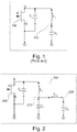
- Figure 1 shows a field-effect transistor (FET) 105 with terminals G (gate), D (drain) and S (source).
- the output capacitance of the FET 105 i.e. the capacitance between the D and S terminals, is C O .
- the Inshin network 110 is arranged in parallel with the output capacitance C O and consists of an inductor L 1 connected in series with a capacitor C 1 .
- EP 1748487 A2 discloses a semiconductor power device and RF signal amplifier comprising a drain matching circuit.
- the dual-band semiconductor RF amplifier device defined by claim 1. Also disclosed is a device comprises (a) a transistor having an output capacitance, (b) a first shunt element arranged in parallel with the output capacitance, the first shunt element comprising a first shunt inductor connected in series with a first shunt capacitor, and (c) a second shunt element arranged in parallel with the first shunt capacitor, the second shunt element comprising a second shunt inductor connected in series with a second shunt capacitor.
- the capacitance of the second shunt capacitor is at least two times the capacitance of the first shunt capacitor, such as between 2 and 20 times the capacitance of the first shunt capacitor, such as between 3 and 10 times the capacitance of the first shunt capacitor, or such as between 4 and 7 times the capacitance of the first shunt capacitor.
- the first aspect is based on the idea that an additional resonance frequency, and consequently impedance matching at a second frequency band, can be provided by arranging a second shunt element in parallel with the first shunt capacitor.
- the second shunt element comprises a second shunt inductor in series with a second shunt capacitor, the latter having a capacitance which is so large that it essentially acts as a short circuit at the RF frequency band of interest.
- the second shunt inductor in combination with the transistor's output capacitance and the first shunt inductor (Inshin) can form an additional resonance circuit and thereby provide impedance matching in a second frequency band, which has a much lower center frequency of operation than that of the primary frequency band.
- the primary frequency band is formed by interaction between the transistor's output capacitance and the first shunt element.
- the second shunt element provides a second resonance frequency (the first resonance frequency is provided by the first shunt inductor (Inshin) and the transistor's output capacitance), such that a dual-band RF amplifier device results.
- the transistor may (in particular) be a FET (field-effect transistor).
- output capacitance may particularly denote the total capacitance between the drain and source terminals in a state, where the transistor is biased by a nominal drain-source dc supply voltage or not connected to any additional circuitry.
- shunt element may particularly denote an element having an electrical impedance and being arranged to shunt some other element(s) or component(s).
- the first and second shunt elements of the amplifier device constitute an output matching circuit.
- This output matching circuit combines with the output capacitance of the transistor to create two separate resonance frequencies, and consequently provides impedance matching in two different RF frequency bands. Thereby, dual-band RF operation is enabled by a simple additional shunt, which is easy to implement and which can be manufactured at low cost.
- the capacitance of the second shunt capacitor is at least five times the capacitance of the first shunt capacitor, such as five times the capacitance of the first shunt capacitor, such as six times the capacitance of the first shunt capacitor, such as eight times the capacitance of the first shunt capacitor, or such as 12 times the capacitance of the first shunt capacitor.
- the second shunt capacitor By designing the second shunt capacitor to have a capacitance, which is significantly larger than the capacitance of the first shunt capacitor, it can be assured that the second shunt capacitor essentially acts as a short circuit in the entire frequency range (RF) of the dual-band amplifier device. Thereby, the second shunt inductor can interact with the remaining circuit elements to resonate at a different resonance frequency than the resonance frequency provided by the first shunt element alone.
- the capacitance of the first shunt capacitor is between 100 pF and 250 pF, such as between 125 pF and 225 pF, such as between 150 pF and 200 pF, such as between 100 pF and 200 pF, such as between 150 pF and 250 pF, such as around 175 pF.
- the value of the first shunt capacitor may also have an effect on the bandwidth of the lower RF frequency band. This is because the first shunt capacitor may form an additional resonance circuit together with the second shunt inductor.
- the capacitance of the second shunt capacitor is between 500 pF and 100 nF, such as between 600 pF and 80 nF, such as between 700 pF and 60 nF, such as between 800 pF and 40 nF, such as between 900 pF and 20 nF, such as between 1 nF and 10 nF, such as around 5 nF.
- the first shunt element is adapted to, in combination with the output capacitance, form a first resonance circuit having a first resonance frequency
- the second shunt element is adapted to, in combination with the output capacitance and the first shunt element, form a second resonance circuit having a second resonance frequency, the second resonance frequency being lower than the first resonance frequency
- the first shunt element transforms impedance from the output of the transistor to the package lead, to an impedance value which is so large (in the high-frequency band), that it can be further transformed to e.g. a 50-Ohm (or an arbitrary impedance if required) environment of the RF PA circuit.
- the second shunt element is designed in conjunction with the choice of values of the first shunt element, so as to allow the amplifier device to operate in frequency band having a lower center frequency than the center frequency of the frequency band provided by the first shunt element alone.
- the first resonance frequency is about 2140 MHz and the second resonance frequency is about 500 MHz.
- the frequency bands of the present embodiment may in particular allow use of the dual-band amplifier device in a base station for mobile communication networks.
- the device may be designed to provide dual-band operation in a wide range of RF bands by appropriately selecting the values for the first and second shunt elements.
- the second shunt capacitor is formed as a high-density capacitor, preferably with low losses and high-breakdown voltage.
- the second shunt capacitor By forming the second shunt capacitor as a high-density capacitor, the second shunt capacitor can be arranged in a compact semiconductor package together with the transistor.
- the first shunt inductor and second shunt inductor are constituted by bonding wires and/or low-loss printed inductors.
- the shunt inductors can be arranged within a small semiconductor package together with the transistor and/or other parts of the dual-band output matching circuit.
- the device further comprises an input matching circuit for providing dual-band input impedance matching.
- the RF performance of the amplifier device can be further improved.
- the input matching circuit comprises (a) a first input matching element arranged between an input terminal and a ground terminal, the first input matching element comprising a first input matching inductor connected in series with a first input matching capacitor, and (b) a second input matching element arranged in parallel with the first input matching capacitor, the second input matching element comprising a second input matching inductor connected in series with a second input matching capacitor, wherein the capacitance of the second input matching capacitor is at least two times the capacitance of the first input matching capacitor.
- the input matching circuit functions in a similar way as described above in connection with the output side of the transistor.
- the input matching circuit interacts with the input capacitance of the transistor and provides two separate impedance matchings at two different RF frequency bands.
- a dual-band RF amplifier comprising a plurality of devices according to the first aspect or any of the above embodiments, wherein the devices are arranged in parallel between an amplifier input terminal and an amplifier output terminal.
- This aspect is based on the idea that a high-power dual-band RF amplifier can be provided in a simple and cost-efficient way by using a plurality of amplifier devices according to the first aspect and/or any of the above embodiments.
- a base station for a mobile communication network.
- the base station is configured to operate the dual-band semiconductor device defined by a preceding aspect.
- a method of manufacturing a dual-band semiconductor RF amplifier device comprises (a) providing a transistor, the transistor having an output capacitance, (b) arranging a first shunt element in parallel with the output capacitance, the first shunt element comprising a first shunt inductor connected in series with a first shunt capacitor, and (c) arranging a second shunt element in parallel with the first shunt capacitor, the second shunt element comprising a second shunt inductor connected in series with a second shunt capacitor, the capacitance of the second shunt capacitor being at least two times the capacitance of the first shunt capacitor.
- This aspect is generally based on the same idea as the first aspect and provides an effective way of manufacturing a compact dual-band semiconductor RF amplifier unit.
- FIG. 2 shows a dual-band semiconductor RF amplifier device 200 in accordance with an embodiment.
- the RF amplifier device 200 comprises a FET 205 with terminals G (gate), D (drain) and S (source).
- the output capacitance of the FET 205 i.e. the capacitance between the D and S terminals, is C O .
- a first shunt element 210 is arranged in parallel with the output capacitance C O and consists of a first shunt inductor L 1 connected in series with a first shunt capacitor C 1 .
- the first shunt element 210 corresponds to the Inshin circuit 110 shown in Figure 1 and previously discussed.
- the dual-band semiconductor RF amplifier device 200 further comprises a second shunt element 220 arranged in parallel with the first capacitor C 1 .
- the second shunt element 220 comprises a second shunt inductor L 2 and a second shunt capacitor C 2 .
- the capacitance of the second shunt capacitor C 2 is significantly larger (by a factor two or more) than the capacitance of the first shunt capacitor C 1 , and essentially constitutes a short circuit at RF frequencies. More specifically, the capacitance of the second shunt capacitor C 2 is preferably in the range from about 500 pF to about 100 nF, while the capacitance of the first shunt capacitor C 1 preferably is in range from about 100 pF to about 250 pF.
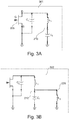
- Figure 3A shows an equivalent circuit 301 of the dual-band semiconductor RF amplifier device 200 of Figure 2 in a high frequency band, i.e. the higher frequency band of the two frequency bands of the dual-band amplifier device 200.
- the impedance of the second shunt inductor L 2 is so large that the second shunt element presents a high impedance, and can be assumed to be essentially disconnected at the higher frequency band.
- the equivalent circuit 301 corresponds to the Inshin-circuit shown in Figure 1 , in which the (first) shunt inductor L 1 and the (first) shunt capacitor C 1 form a resonance circuit with the output capacitance C O of the FET 205.
- FIG. 3B shows an equivalent circuit 302 of the dual-band semiconductor RF amplifier device 200 of Figure 2 in a low frequency band, i.e. the lower frequency band of the two frequency bands of the dual-band amplifier device 200.
- the second shunt inductor L 2 contributes to the resonance circuit which accordingly in this case consists of the second shunt inductor L2, the output capacitance C O of the FET 205, the first shunt capacitor C 1 , and the first shunt inductor L 1 .
- This resonance circuit has a lower resonance frequency than the one shown in Figure 3A .
- the second shunt capacitor C 2 is not shown in the equivalent circuit 302 as it essentially constitutes a short circuit (zero impedance) at RF frequencies.
- the dual-band amplifier device 205 is capable of operating in two distinct frequency bands, e.g. at 500 MHz (low band) and 2140 MHz (high band) or in any other desirable RF bands, depending on the specific application of the amplifier.
- Figure 4 shows an RF amplifier device 200 further comprising an input matching circuit 430 and an output matching circuit 440. Furthermore, Figure 4 shows four alternative input matching circuits 431, 432, 433, and 434, each of which may be used as the input matching circuit 430, and one specific embodiment 441 for use as the output matching circuit 440.
- the input matching circuit 431 is a so-called single-section low pass matching circuit comprising a capacitor C 11 and an inductor L 11 .
- the inductor L 11 is arranged between an input terminal 450 and the gate terminal of the FET 205.
- the capacitor C 11 is arranged between the input terminal 450 and ground.
- impedance matching at the transistor input (gate terminal) is only possible at one frequency. Impedance matching can be provided at the high-band for power gain, while at the low-band the device can be mismatched since there is relatively more gain at lower frequencies.
- the input matching circuit 432 is a so-called double-section low pass matching circuit comprising capacitors C 21 and C 22 and inductors L 21 and L 22 .
- the inductors L 21 and L 22 are arranged in series between input terminal 450 and the gate terminal of the FET 205.
- the capacitor C 21 is arranged between the junction of the inductors L 21 and L 22 and ground.
- the capacitor C 22 is arranged between the input terminal 450 and ground.
- the input matching circuit 433 is a so-called low pass + Inshin matching circuit comprising capacitors C 31 and C 32 and inductors L 31 and L 32 .
- the capacitor C 31 and the inductor L 31 are arranged in series between the gate terminal of the FET 205 and ground and thereby constitute an Inshin-circuit.
- the inductor L 32 is arranged between the input terminal 450 and the the gate terminal of the FET 205.
- the capacitor C 32 is arranged between the input terminal 450 and ground. Thereby, the inductor L 32 and the capacitor C 32 constitute a low pass circuit.
- Inshin matching can be used to provide impedance match at the low-band
- low-pass can be used to provide impedance match at the high-band. It is easier to obtain impedance transformation using low-pass at the high-band and with Inshin at the low band.
- the input matching circuit 434 is a dual-band matching circuit based on the same principle that is used on the output side of the FET 205 (see detailed description above in connection with Figures 2 , 3A and 3B ).
- the inductor L 41 and the capacitor C 41 are arranged in series between the gate terminal of the FET 205 to form an Inshin-circuit similar to that formed by the inductor L 1 and the capacitor C 1 between the drain terminal of the FET and ground.
- the inductor L 42 and capacitor C 42 are arranged in series between the junction between the inductor L 41 and the capacitor C 41 and ground.
- L 42 and C 42 correspond to L 2 and C 2 on the output side of the FET 205.
- an optional output matching circuit 440 is arranged between the drain terminal of the FET 205 and output terminal 451.
- the optional output matching circuit 440 may e.g. be a low-pass circuit 441 comprising inductor L 5 and capacitor C 5 in applications that require higher impedance at the RF output package lead.
- FIG. 5 shows an RF amplifier 500 comprising two identical dual-band RF amplifier devices 500a and 500b in accordance with an embodiment.
- Each of the two dual-band RF amplifier devices 500a and 500b work in accordance with the principles discussed above in connection with dual-band RF amplifier device 200 and differ from this only in the provision of an input matching circuit.
- DC voltages V1 and V2 are respectively provided at the input side and the output side of the amplifier 500 via respective RF chokes L C1 and L C2 .
- the two dual-band RF amplifier devices are arranged in parallel through the connection on the RF lead of the package.
- the amplifier 500 is fed with input RF signal 560 and connected to output load 561. It should be noted that this embodiment may be modified if desirable by adding further dual-band RF amplifier devices in parallel with the devices 500a and 500b.
- the transistor and matching circuits are preferably formed as a single integrated device or package.
- the various inductances, in particular L 1 and L 2 are constituted by bonding wires. Thereby, a simple and powerful dual-band RF amplifier is provided.
Landscapes
- Engineering & Computer Science (AREA)
- Power Engineering (AREA)
- Microelectronics & Electronic Packaging (AREA)
- Amplifiers (AREA)
Claims (10)
- Dispositif amplificateur RF à semi-conducteurs et à double bande, le dispositif comprenant
un transistor (205) qui possède une capacitance de sortie (CO) et une capacitance d'entrée,
un premier élément de shunt (210) prévu en parallèle avec la capacitance de sortie, le premier élément de shunt comprenant un premier inducteur de shunt (L1) relié en série avec un premier condensateur de shunt (C1), et
un second élément de shunt (220) prévu en parallèle avec le premier condensateur de shunt, le second élément de shunt comprenant un second inducteur de shunt (L2) relié en série avec un second condensateur de shunt (C2),
le dispositif amplificateur RF à semi-conducteurs et à double bande étant capable de fonctionner sur deux bandes de fréquences distinctes ;
dans lequel une capacitance du second condensateur de shunt (C2) est telle qu'elle forme effectivement un court-circuit aux fréquences RF ;
dans lequel le premier inducteur de shunt, le second inducteur de shunt, et le premier condensateur de shunt sont configurés afin de former une inductance effective qui résonne avec la capacitance de sortie sur chacune des deux bandes de fréquences distinctes,
dans lequel la capacitance du second condensateur de shunt (C2) est au moins deux fois égale à la capacitance du premier condensateur de shunt (C1) ;
qui comprend en outre un circuit d'adaptation d'entrée qui interagit avec la capacitance d'entrée du transistor et fournit deux adaptations d'entrée distinctes sur les deux bandes de fréquences distinctes. - Dispositif selon la revendication précédente, dans lequel la capacitance du second condensateur de shunt (C2) est au moins cinq fois égale à la capacitance du premier condensateur de shunt (C1).
- Dispositif selon l'une quelconque des revendications précédentes, dans lequel la capacitance du premier condensateur de shunt (C1) est comprise entre 100 pF et 250 pF, et la capacitance du second condensateur de shunt (C2) est comprise entre 500 pF et 100 nF.
- Dispositif selon l'une quelconque des revendications précédentes, dans lequel le premier élément de shunt (210) est adapté, en combinaison avec la capacitance de sortie (CO), afin de former un premier circuit de résonance qui présente une première fréquence de résonance, et le second élément de shunt (220) est adapté, en combinaison avec la capacitance de sortie (CO) et le premier élément de shunt (210), afin de former un second circuit de résonance qui présente une seconde fréquence de résonance, la seconde fréquence de résonance étant inférieure à la première fréquence de résonance.
- Dispositif selon la revendication 4, dans lequel la première fréquence de résonance est de 2140 MHz et la seconde fréquence de résonance est de 500 MHz.
- Dispositif selon l'une quelconque des revendications précédentes, dans lequel le second condensateur shunt (C2) est formé comme un condensateur à haute densité.
- Dispositif selon l'une quelconque des revendications précédentes, dans lequel le premier inducteur de shunt (L1) et le second inducteur de shunt (L2) sont constitués de fils de liaison et/ou d'inducteurs imprimés à faible perte.
- Dispositif selon l'une quelconque des revendications précédentes, qui comprend en outre un circuit d'adaptation d'entrée (434) destiné à assurer une adaptation d'impédance d'entrée en double bande.
- Dispositif selon la revendication précédente, dans lequel le circuit d'adaptation d'entrée (434) comprend
un premier élément d'adaptation d'entrée prévu entre une borne d'entrée et une borne de masse, le premier élément d'adaptation d'entrée comprenant un premier inducteur d'adaptation d'entrée (L41) relié en série avec un premier condensateur d'adaptation d'entrée (C41), et
un second élément d'adaptation d'entrée prévu en parallèle avec le premier condensateur d'adaptation d'entrée, le second élément d'adaptation d'entrée comprenant un second inducteur d'adaptation d'entrée (L42) relié en série avec un second condensateur d'adaptation d'entrée (C42),
dans lequel la capacitance du second condensateur d'adaptation d'entrée (C42) est au moins deux fois égale à la capacitance du premier condensateur d'adaptation d'entrée (C41). - Amplificateur RF à double bande, l'amplificateur RF à double bande comprenant une pluralité de dispositifs d'amplification identiques (200, 500a, 500b) selon l'une quelconque des revendications précédentes, les dispositifs étant prévus en parallèle entre une borne d'entrée d'amplificateur (450) et une borne de sortie d'amplificateur (451).
Priority Applications (2)
| Application Number | Priority Date | Filing Date | Title |
|---|---|---|---|
| EP13166882.4A EP2802075B1 (fr) | 2013-05-07 | 2013-05-07 | Dispositif amplificateur RF semi-conducteur à double bande |
| US14/267,715 US9450545B2 (en) | 2013-05-07 | 2014-05-01 | Dual-band semiconductor RF amplifier device |
Applications Claiming Priority (1)
| Application Number | Priority Date | Filing Date | Title |
|---|---|---|---|
| EP13166882.4A EP2802075B1 (fr) | 2013-05-07 | 2013-05-07 | Dispositif amplificateur RF semi-conducteur à double bande |
Publications (2)
| Publication Number | Publication Date |
|---|---|
| EP2802075A1 EP2802075A1 (fr) | 2014-11-12 |
| EP2802075B1 true EP2802075B1 (fr) | 2017-02-15 |
Family
ID=48236774
Family Applications (1)
| Application Number | Title | Priority Date | Filing Date |
|---|---|---|---|
| EP13166882.4A Active EP2802075B1 (fr) | 2013-05-07 | 2013-05-07 | Dispositif amplificateur RF semi-conducteur à double bande |
Country Status (2)
| Country | Link |
|---|---|
| US (1) | US9450545B2 (fr) |
| EP (1) | EP2802075B1 (fr) |
Families Citing this family (7)
| Publication number | Priority date | Publication date | Assignee | Title |
|---|---|---|---|---|
| US8659359B2 (en) | 2010-04-22 | 2014-02-25 | Freescale Semiconductor, Inc. | RF power transistor circuit |
| US9281283B2 (en) | 2012-09-12 | 2016-03-08 | Freescale Semiconductor, Inc. | Semiconductor devices with impedance matching-circuits |
| US10432152B2 (en) | 2015-05-22 | 2019-10-01 | Nxp Usa, Inc. | RF amplifier output circuit device with integrated current path, and methods of manufacture thereof |
| US9571044B1 (en) * | 2015-10-21 | 2017-02-14 | Nxp Usa, Inc. | RF power transistors with impedance matching circuits, and methods of manufacture thereof |
| US9692363B2 (en) | 2015-10-21 | 2017-06-27 | Nxp Usa, Inc. | RF power transistors with video bandwidth circuits, and methods of manufacture thereof |
| CN107547054B (zh) * | 2017-09-07 | 2020-03-27 | 苏州远创达科技有限公司 | 分离式补偿电感内匹配功率放大器 |
| CN111030614B (zh) * | 2019-12-11 | 2023-10-27 | 电子科技大学 | 一种跨导增强型毫米波低噪声放大器 |
Family Cites Families (18)
| Publication number | Priority date | Publication date | Assignee | Title |
|---|---|---|---|---|
| US3969752A (en) * | 1973-12-03 | 1976-07-13 | Power Hybrids, Inc. | Hybrid transistor |
| US4464636A (en) * | 1983-01-05 | 1984-08-07 | Zenith Electronics Corporation | Wideband IF amplifier with complementary GaAs FET-bipolar transistor combination |
| US5117203A (en) * | 1990-12-13 | 1992-05-26 | General Electric Company | Phase stable limiting power amplifier |
| JPH06188654A (ja) * | 1992-12-18 | 1994-07-08 | Fujitsu Ltd | 高周波増幅器 |
| AU2001249730A1 (en) | 2000-03-28 | 2001-10-08 | California Institute Of Technology | Concurrent multi-band low noise amplifier architecture |
| US7119623B2 (en) | 2002-02-01 | 2006-10-10 | Koninklijke Philips Electronics N.V. | Output circuit for a semiconductor amplifier element |
| EP1490907A1 (fr) * | 2002-03-21 | 2004-12-29 | Koninklijke Philips Electronics N.V. | Dispositif amplificateur de puissance |
| US6822321B2 (en) | 2002-09-30 | 2004-11-23 | Cree Microwave, Inc. | Packaged RF power transistor having RF bypassing/output matching network |
| WO2006016299A1 (fr) * | 2004-08-09 | 2006-02-16 | Koninklijke Philips Electronics N.V. | Amplificateur integre de classe f a compensation de capacite de sortie parasite |
| US7564303B2 (en) * | 2005-07-26 | 2009-07-21 | Infineon Technologies Ag | Semiconductor power device and RF signal amplifier |
| US7372334B2 (en) * | 2005-07-26 | 2008-05-13 | Infineon Technologies Ag | Output match transistor |
| US7719141B2 (en) * | 2006-11-16 | 2010-05-18 | Star Rf, Inc. | Electronic switch network |
| US20080231373A1 (en) * | 2007-03-20 | 2008-09-25 | Hafizur Rahman | Output Circuit |
| WO2009139680A1 (fr) * | 2008-05-16 | 2009-11-19 | Telefonaktiebolaget L M Ericsson (Publ) | Decouplage de bande de base de transistors de puissance radiofrequences |
| US7986184B2 (en) | 2009-12-18 | 2011-07-26 | Nxp B.V. | Radio frequency amplifier with effective decoupling |
| US8299856B2 (en) * | 2010-12-20 | 2012-10-30 | Infineon Technologies Ag | Power transistor output match network with high Q RF path and low Q low frequency path |
| US9281283B2 (en) * | 2012-09-12 | 2016-03-08 | Freescale Semiconductor, Inc. | Semiconductor devices with impedance matching-circuits |
| EP2876810B1 (fr) * | 2013-11-22 | 2016-04-13 | Samba Holdco Netherlands B.V. | Amplificateur de Doherty |
-
2013
- 2013-05-07 EP EP13166882.4A patent/EP2802075B1/fr active Active
-
2014
- 2014-05-01 US US14/267,715 patent/US9450545B2/en active Active
Non-Patent Citations (1)
| Title |
|---|
| None * |
Also Published As
| Publication number | Publication date |
|---|---|
| EP2802075A1 (fr) | 2014-11-12 |
| US9450545B2 (en) | 2016-09-20 |
| US20140333385A1 (en) | 2014-11-13 |
Similar Documents
| Publication | Publication Date | Title |
|---|---|---|
| US9450545B2 (en) | Dual-band semiconductor RF amplifier device | |
| US9698749B2 (en) | Impedance matching device with coupled resonator structure | |
| KR102355260B1 (ko) | 다중 고조파 근사에 기초하는 전력 증폭기 효율과 관련된 회로 및 방법 | |
| US6046641A (en) | Parallel HV MOSFET high power stable amplifier | |
| KR100841119B1 (ko) | 반도체 전력 디바이스 및 광대역 고주파 (rf) 신호증폭기 | |
| CN108233881B (zh) | 放大器电路和经封装的放大器电路 | |
| CN107528554B (zh) | 紧凑的希莱克合并器和阻抗匹配电路 | |
| KR102497507B1 (ko) | 광대역 고조파 매칭 회로망 | |
| EP2461335A1 (fr) | Transformateur de fil de connexion | |
| CN107332518B (zh) | 一种宽带多赫蒂功率放大器 | |
| JP2006501678A (ja) | Rfバイパス・出力マッチングネットワークを有するパッケージに収納されたrfパワートランジスタ | |
| KR101079474B1 (ko) | 내부 정합 인덕터를 공유하는 무선 통신을 위한 병렬 증폭 장치 | |
| WO2014068351A2 (fr) | Étage d'amplification et amplificateur de puissance à large bande | |
| EP2838195B1 (fr) | Circuit de combinateur pour amplificateur de puissance de classe E à déphasage | |
| EP3504792B1 (fr) | Amplificateur de puissance rf mis sous boîtier à densité de puissance élevée | |
| CN111510077A (zh) | 一种宽带多赫蒂放大器 | |
| Wei et al. | Investigation of wideband load transformation networks for class-E switching-mode power amplifiers | |
| CN110829988A (zh) | 具有宽带阻抗匹配的放大器和其制造方法 | |
| CN110176909B (zh) | 功率放大器 | |
| WO2002056462A9 (fr) | Amelioration de la largeur de bande et du gain pour boitier d'amplificateur de puissance en haute frequence | |
| US8203399B2 (en) | Transformer capable of removing harmonic components | |
| US9748907B2 (en) | Output impedance-matching network having harmonic-prevention circuitry | |
| CN104733810B (zh) | 开关电路及高频模块 | |
| Lee et al. | A 1.8-GHz 2-watt fully integrated CMOS push-pull parallel-combined power amplifier design | |
| Khorshidian et al. | A fully-integrated 2.6 GHz stacked switching power amplifier in 45nm SOI CMOS with> 2W output power and 43.5% efficiency |
Legal Events
| Date | Code | Title | Description |
|---|---|---|---|
| PUAI | Public reference made under article 153(3) epc to a published international application that has entered the european phase |
Free format text: ORIGINAL CODE: 0009012 |
|
| 17P | Request for examination filed |
Effective date: 20140326 |
|
| AK | Designated contracting states |
Kind code of ref document: A1 Designated state(s): AL AT BE BG CH CY CZ DE DK EE ES FI FR GB GR HR HU IE IS IT LI LT LU LV MC MK MT NL NO PL PT RO RS SE SI SK SM TR |
|
| AX | Request for extension of the european patent |
Extension state: BA ME |
|
| TPAC | Observations filed by third parties |
Free format text: ORIGINAL CODE: EPIDOSNTIPA |
|
| RBV | Designated contracting states (corrected) |
Designated state(s): AL AT BE BG CH CY CZ DE DK EE ES FI FR GB GR HR HU IE IS IT LI LT LU LV MC MK MT NL NO PL PT RO RS SE SI SK SM TR |
|
| RAP1 | Party data changed (applicant data changed or rights of an application transferred) |
Owner name: SAMBA HOLDCO NETHERLANDS B.V. |
|
| RAP1 | Party data changed (applicant data changed or rights of an application transferred) |
Owner name: AMPLEON NETHERLANDS B.V. |
|
| REG | Reference to a national code |
Ref country code: DE Ref legal event code: R079 Ref document number: 602013017434 Country of ref document: DE Free format text: PREVIOUS MAIN CLASS: H03F0003191000 Ipc: H03F0003210000 |
|
| GRAP | Despatch of communication of intention to grant a patent |
Free format text: ORIGINAL CODE: EPIDOSNIGR1 |
|
| RIC1 | Information provided on ipc code assigned before grant |
Ipc: H03F 3/21 20060101AFI20160810BHEP Ipc: H03F 3/193 20060101ALI20160810BHEP Ipc: H03F 3/195 20060101ALI20160810BHEP |
|
| INTG | Intention to grant announced |
Effective date: 20160906 |
|
| GRAS | Grant fee paid |
Free format text: ORIGINAL CODE: EPIDOSNIGR3 |
|
| GRAA | (expected) grant |
Free format text: ORIGINAL CODE: 0009210 |
|
| AK | Designated contracting states |
Kind code of ref document: B1 Designated state(s): AL AT BE BG CH CY CZ DE DK EE ES FI FR GB GR HR HU IE IS IT LI LT LU LV MC MK MT NL NO PL PT RO RS SE SI SK SM TR |
|
| REG | Reference to a national code |
Ref country code: CH Ref legal event code: EP Ref country code: GB Ref legal event code: FG4D |
|
| REG | Reference to a national code |
Ref country code: IE Ref legal event code: FG4D |
|
| REG | Reference to a national code |
Ref country code: AT Ref legal event code: REF Ref document number: 868405 Country of ref document: AT Kind code of ref document: T Effective date: 20170315 |
|
| REG | Reference to a national code |
Ref country code: DE Ref legal event code: R096 Ref document number: 602013017434 Country of ref document: DE |
|
| REG | Reference to a national code |
Ref country code: NL Ref legal event code: FP |
|
| REG | Reference to a national code |
Ref country code: LT Ref legal event code: MG4D |
|
| REG | Reference to a national code |
Ref country code: AT Ref legal event code: MK05 Ref document number: 868405 Country of ref document: AT Kind code of ref document: T Effective date: 20170215 |
|
| PG25 | Lapsed in a contracting state [announced via postgrant information from national office to epo] |
Ref country code: NO Free format text: LAPSE BECAUSE OF FAILURE TO SUBMIT A TRANSLATION OF THE DESCRIPTION OR TO PAY THE FEE WITHIN THE PRESCRIBED TIME-LIMIT Effective date: 20170515 Ref country code: GR Free format text: LAPSE BECAUSE OF FAILURE TO SUBMIT A TRANSLATION OF THE DESCRIPTION OR TO PAY THE FEE WITHIN THE PRESCRIBED TIME-LIMIT Effective date: 20170516 Ref country code: LT Free format text: LAPSE BECAUSE OF FAILURE TO SUBMIT A TRANSLATION OF THE DESCRIPTION OR TO PAY THE FEE WITHIN THE PRESCRIBED TIME-LIMIT Effective date: 20170215 Ref country code: FI Free format text: LAPSE BECAUSE OF FAILURE TO SUBMIT A TRANSLATION OF THE DESCRIPTION OR TO PAY THE FEE WITHIN THE PRESCRIBED TIME-LIMIT Effective date: 20170215 Ref country code: HR Free format text: LAPSE BECAUSE OF FAILURE TO SUBMIT A TRANSLATION OF THE DESCRIPTION OR TO PAY THE FEE WITHIN THE PRESCRIBED TIME-LIMIT Effective date: 20170215 |
|
| PG25 | Lapsed in a contracting state [announced via postgrant information from national office to epo] |
Ref country code: SE Free format text: LAPSE BECAUSE OF FAILURE TO SUBMIT A TRANSLATION OF THE DESCRIPTION OR TO PAY THE FEE WITHIN THE PRESCRIBED TIME-LIMIT Effective date: 20170215 Ref country code: AT Free format text: LAPSE BECAUSE OF FAILURE TO SUBMIT A TRANSLATION OF THE DESCRIPTION OR TO PAY THE FEE WITHIN THE PRESCRIBED TIME-LIMIT Effective date: 20170215 Ref country code: LU Free format text: LAPSE BECAUSE OF NON-PAYMENT OF DUE FEES Effective date: 20170531 Ref country code: LV Free format text: LAPSE BECAUSE OF FAILURE TO SUBMIT A TRANSLATION OF THE DESCRIPTION OR TO PAY THE FEE WITHIN THE PRESCRIBED TIME-LIMIT Effective date: 20170215 Ref country code: BG Free format text: LAPSE BECAUSE OF FAILURE TO SUBMIT A TRANSLATION OF THE DESCRIPTION OR TO PAY THE FEE WITHIN THE PRESCRIBED TIME-LIMIT Effective date: 20170515 Ref country code: RS Free format text: LAPSE BECAUSE OF FAILURE TO SUBMIT A TRANSLATION OF THE DESCRIPTION OR TO PAY THE FEE WITHIN THE PRESCRIBED TIME-LIMIT Effective date: 20170215 Ref country code: ES Free format text: LAPSE BECAUSE OF FAILURE TO SUBMIT A TRANSLATION OF THE DESCRIPTION OR TO PAY THE FEE WITHIN THE PRESCRIBED TIME-LIMIT Effective date: 20170215 Ref country code: PT Free format text: LAPSE BECAUSE OF FAILURE TO SUBMIT A TRANSLATION OF THE DESCRIPTION OR TO PAY THE FEE WITHIN THE PRESCRIBED TIME-LIMIT Effective date: 20170615 |
|
| PG25 | Lapsed in a contracting state [announced via postgrant information from national office to epo] |
Ref country code: EE Free format text: LAPSE BECAUSE OF FAILURE TO SUBMIT A TRANSLATION OF THE DESCRIPTION OR TO PAY THE FEE WITHIN THE PRESCRIBED TIME-LIMIT Effective date: 20170215 Ref country code: IT Free format text: LAPSE BECAUSE OF FAILURE TO SUBMIT A TRANSLATION OF THE DESCRIPTION OR TO PAY THE FEE WITHIN THE PRESCRIBED TIME-LIMIT Effective date: 20170215 Ref country code: RO Free format text: LAPSE BECAUSE OF FAILURE TO SUBMIT A TRANSLATION OF THE DESCRIPTION OR TO PAY THE FEE WITHIN THE PRESCRIBED TIME-LIMIT Effective date: 20170215 Ref country code: SK Free format text: LAPSE BECAUSE OF FAILURE TO SUBMIT A TRANSLATION OF THE DESCRIPTION OR TO PAY THE FEE WITHIN THE PRESCRIBED TIME-LIMIT Effective date: 20170215 Ref country code: CZ Free format text: LAPSE BECAUSE OF FAILURE TO SUBMIT A TRANSLATION OF THE DESCRIPTION OR TO PAY THE FEE WITHIN THE PRESCRIBED TIME-LIMIT Effective date: 20170215 |
|
| REG | Reference to a national code |
Ref country code: DE Ref legal event code: R097 Ref document number: 602013017434 Country of ref document: DE |
|
| PG25 | Lapsed in a contracting state [announced via postgrant information from national office to epo] |
Ref country code: DK Free format text: LAPSE BECAUSE OF FAILURE TO SUBMIT A TRANSLATION OF THE DESCRIPTION OR TO PAY THE FEE WITHIN THE PRESCRIBED TIME-LIMIT Effective date: 20170215 Ref country code: PL Free format text: LAPSE BECAUSE OF FAILURE TO SUBMIT A TRANSLATION OF THE DESCRIPTION OR TO PAY THE FEE WITHIN THE PRESCRIBED TIME-LIMIT Effective date: 20170215 Ref country code: SM Free format text: LAPSE BECAUSE OF FAILURE TO SUBMIT A TRANSLATION OF THE DESCRIPTION OR TO PAY THE FEE WITHIN THE PRESCRIBED TIME-LIMIT Effective date: 20170215 |
|
| PLBE | No opposition filed within time limit |
Free format text: ORIGINAL CODE: 0009261 |
|
| STAA | Information on the status of an ep patent application or granted ep patent |
Free format text: STATUS: NO OPPOSITION FILED WITHIN TIME LIMIT |
|
| REG | Reference to a national code |
Ref country code: CH Ref legal event code: PL |
|
| 26N | No opposition filed |
Effective date: 20171116 |
|
| GBPC | Gb: european patent ceased through non-payment of renewal fee |
Effective date: 20170515 |
|
| PG25 | Lapsed in a contracting state [announced via postgrant information from national office to epo] |
Ref country code: MC Free format text: LAPSE BECAUSE OF FAILURE TO SUBMIT A TRANSLATION OF THE DESCRIPTION OR TO PAY THE FEE WITHIN THE PRESCRIBED TIME-LIMIT Effective date: 20170215 |
|
| REG | Reference to a national code |
Ref country code: IE Ref legal event code: MM4A |
|
| PG25 | Lapsed in a contracting state [announced via postgrant information from national office to epo] |
Ref country code: LI Free format text: LAPSE BECAUSE OF NON-PAYMENT OF DUE FEES Effective date: 20170531 Ref country code: SI Free format text: LAPSE BECAUSE OF FAILURE TO SUBMIT A TRANSLATION OF THE DESCRIPTION OR TO PAY THE FEE WITHIN THE PRESCRIBED TIME-LIMIT Effective date: 20170215 Ref country code: CH Free format text: LAPSE BECAUSE OF NON-PAYMENT OF DUE FEES Effective date: 20170531 |
|
| REG | Reference to a national code |
Ref country code: FR Ref legal event code: ST Effective date: 20180131 |
|
| PG25 | Lapsed in a contracting state [announced via postgrant information from national office to epo] |
Ref country code: LU Free format text: LAPSE BECAUSE OF NON-PAYMENT OF DUE FEES Effective date: 20170507 |
|
| REG | Reference to a national code |
Ref country code: BE Ref legal event code: MM Effective date: 20170531 |
|
| PG25 | Lapsed in a contracting state [announced via postgrant information from national office to epo] |
Ref country code: IE Free format text: LAPSE BECAUSE OF NON-PAYMENT OF DUE FEES Effective date: 20170507 Ref country code: GB Free format text: LAPSE BECAUSE OF NON-PAYMENT OF DUE FEES Effective date: 20170515 |
|
| PG25 | Lapsed in a contracting state [announced via postgrant information from national office to epo] |
Ref country code: FR Free format text: LAPSE BECAUSE OF NON-PAYMENT OF DUE FEES Effective date: 20170531 |
|
| PG25 | Lapsed in a contracting state [announced via postgrant information from national office to epo] |
Ref country code: BE Free format text: LAPSE BECAUSE OF NON-PAYMENT OF DUE FEES Effective date: 20170531 |
|
| PG25 | Lapsed in a contracting state [announced via postgrant information from national office to epo] |
Ref country code: MT Free format text: LAPSE BECAUSE OF NON-PAYMENT OF DUE FEES Effective date: 20170507 |
|
| PG25 | Lapsed in a contracting state [announced via postgrant information from national office to epo] |
Ref country code: HU Free format text: LAPSE BECAUSE OF FAILURE TO SUBMIT A TRANSLATION OF THE DESCRIPTION OR TO PAY THE FEE WITHIN THE PRESCRIBED TIME-LIMIT; INVALID AB INITIO Effective date: 20130507 |
|
| PG25 | Lapsed in a contracting state [announced via postgrant information from national office to epo] |
Ref country code: CY Free format text: LAPSE BECAUSE OF FAILURE TO SUBMIT A TRANSLATION OF THE DESCRIPTION OR TO PAY THE FEE WITHIN THE PRESCRIBED TIME-LIMIT Effective date: 20170215 |
|
| PG25 | Lapsed in a contracting state [announced via postgrant information from national office to epo] |
Ref country code: MK Free format text: LAPSE BECAUSE OF FAILURE TO SUBMIT A TRANSLATION OF THE DESCRIPTION OR TO PAY THE FEE WITHIN THE PRESCRIBED TIME-LIMIT Effective date: 20170215 |
|
| PG25 | Lapsed in a contracting state [announced via postgrant information from national office to epo] |
Ref country code: TR Free format text: LAPSE BECAUSE OF FAILURE TO SUBMIT A TRANSLATION OF THE DESCRIPTION OR TO PAY THE FEE WITHIN THE PRESCRIBED TIME-LIMIT Effective date: 20170215 |
|
| PG25 | Lapsed in a contracting state [announced via postgrant information from national office to epo] |
Ref country code: AL Free format text: LAPSE BECAUSE OF FAILURE TO SUBMIT A TRANSLATION OF THE DESCRIPTION OR TO PAY THE FEE WITHIN THE PRESCRIBED TIME-LIMIT Effective date: 20170215 Ref country code: IS Free format text: LAPSE BECAUSE OF FAILURE TO SUBMIT A TRANSLATION OF THE DESCRIPTION OR TO PAY THE FEE WITHIN THE PRESCRIBED TIME-LIMIT Effective date: 20170615 |
|
| P01 | Opt-out of the competence of the unified patent court (upc) registered |
Effective date: 20230526 |
|
| PGFP | Annual fee paid to national office [announced via postgrant information from national office to epo] |
Ref country code: NL Payment date: 20230526 Year of fee payment: 11 Ref country code: DE Payment date: 20230530 Year of fee payment: 11 |