EP2802054A1 - Switching arrangement for inverter, and inverter - Google Patents
Switching arrangement for inverter, and inverter Download PDFInfo
- Publication number
- EP2802054A1 EP2802054A1 EP20130166951 EP13166951A EP2802054A1 EP 2802054 A1 EP2802054 A1 EP 2802054A1 EP 20130166951 EP20130166951 EP 20130166951 EP 13166951 A EP13166951 A EP 13166951A EP 2802054 A1 EP2802054 A1 EP 2802054A1
- Authority
- EP
- European Patent Office
- Prior art keywords
- inverter
- direct current
- controllable switch
- current pole
- predetermined threshold
- Prior art date
- Legal status (The legal status is an assumption and is not a legal conclusion. Google has not performed a legal analysis and makes no representation as to the accuracy of the status listed.)
- Granted
Links
Images


Classifications
-
- H—ELECTRICITY
- H02—GENERATION; CONVERSION OR DISTRIBUTION OF ELECTRIC POWER
- H02M—APPARATUS FOR CONVERSION BETWEEN AC AND AC, BETWEEN AC AND DC, OR BETWEEN DC AND DC, AND FOR USE WITH MAINS OR SIMILAR POWER SUPPLY SYSTEMS; CONVERSION OF DC OR AC INPUT POWER INTO SURGE OUTPUT POWER; CONTROL OR REGULATION THEREOF
- H02M7/00—Conversion of ac power input into dc power output; Conversion of dc power input into ac power output
- H02M7/42—Conversion of dc power input into ac power output without possibility of reversal
- H02M7/44—Conversion of dc power input into ac power output without possibility of reversal by static converters
- H02M7/48—Conversion of dc power input into ac power output without possibility of reversal by static converters using discharge tubes with control electrode or semiconductor devices with control electrode
- H02M7/483—Converters with outputs that each can have more than two voltages levels
- H02M7/487—Neutral point clamped inverters
-
- H—ELECTRICITY
- H02—GENERATION; CONVERSION OR DISTRIBUTION OF ELECTRIC POWER
- H02J—CIRCUIT ARRANGEMENTS OR SYSTEMS FOR SUPPLYING OR DISTRIBUTING ELECTRIC POWER; SYSTEMS FOR STORING ELECTRIC ENERGY
- H02J3/00—Circuit arrangements for ac mains or ac distribution networks
- H02J3/38—Arrangements for parallely feeding a single network by two or more generators, converters or transformers
- H02J3/381—Dispersed generators
-
- H—ELECTRICITY
- H02—GENERATION; CONVERSION OR DISTRIBUTION OF ELECTRIC POWER
- H02M—APPARATUS FOR CONVERSION BETWEEN AC AND AC, BETWEEN AC AND DC, OR BETWEEN DC AND DC, AND FOR USE WITH MAINS OR SIMILAR POWER SUPPLY SYSTEMS; CONVERSION OF DC OR AC INPUT POWER INTO SURGE OUTPUT POWER; CONTROL OR REGULATION THEREOF
- H02M1/00—Details of apparatus for conversion
- H02M1/12—Arrangements for reducing harmonics from ac input or output
- H02M1/126—Arrangements for reducing harmonics from ac input or output using passive filters
-
- H—ELECTRICITY
- H02—GENERATION; CONVERSION OR DISTRIBUTION OF ELECTRIC POWER
- H02M—APPARATUS FOR CONVERSION BETWEEN AC AND AC, BETWEEN AC AND DC, OR BETWEEN DC AND DC, AND FOR USE WITH MAINS OR SIMILAR POWER SUPPLY SYSTEMS; CONVERSION OF DC OR AC INPUT POWER INTO SURGE OUTPUT POWER; CONTROL OR REGULATION THEREOF
- H02M7/00—Conversion of ac power input into dc power output; Conversion of dc power input into ac power output
- H02M7/42—Conversion of dc power input into ac power output without possibility of reversal
- H02M7/44—Conversion of dc power input into ac power output without possibility of reversal by static converters
- H02M7/48—Conversion of dc power input into ac power output without possibility of reversal by static converters using discharge tubes with control electrode or semiconductor devices with control electrode
- H02M7/483—Converters with outputs that each can have more than two voltages levels
-
- H—ELECTRICITY
- H02—GENERATION; CONVERSION OR DISTRIBUTION OF ELECTRIC POWER
- H02J—CIRCUIT ARRANGEMENTS OR SYSTEMS FOR SUPPLYING OR DISTRIBUTING ELECTRIC POWER; SYSTEMS FOR STORING ELECTRIC ENERGY
- H02J2300/00—Systems for supplying or distributing electric power characterised by decentralized, dispersed, or local generation
- H02J2300/20—The dispersed energy generation being of renewable origin
- H02J2300/22—The renewable source being solar energy
- H02J2300/24—The renewable source being solar energy of photovoltaic origin
-
- H—ELECTRICITY
- H02—GENERATION; CONVERSION OR DISTRIBUTION OF ELECTRIC POWER
- H02M—APPARATUS FOR CONVERSION BETWEEN AC AND AC, BETWEEN AC AND DC, OR BETWEEN DC AND DC, AND FOR USE WITH MAINS OR SIMILAR POWER SUPPLY SYSTEMS; CONVERSION OF DC OR AC INPUT POWER INTO SURGE OUTPUT POWER; CONTROL OR REGULATION THEREOF
- H02M1/00—Details of apparatus for conversion
- H02M1/12—Arrangements for reducing harmonics from ac input or output
- H02M1/123—Suppression of common mode voltage or current
-
- Y—GENERAL TAGGING OF NEW TECHNOLOGICAL DEVELOPMENTS; GENERAL TAGGING OF CROSS-SECTIONAL TECHNOLOGIES SPANNING OVER SEVERAL SECTIONS OF THE IPC; TECHNICAL SUBJECTS COVERED BY FORMER USPC CROSS-REFERENCE ART COLLECTIONS [XRACs] AND DIGESTS
- Y02—TECHNOLOGIES OR APPLICATIONS FOR MITIGATION OR ADAPTATION AGAINST CLIMATE CHANGE
- Y02E—REDUCTION OF GREENHOUSE GAS [GHG] EMISSIONS, RELATED TO ENERGY GENERATION, TRANSMISSION OR DISTRIBUTION
- Y02E10/00—Energy generation through renewable energy sources
- Y02E10/50—Photovoltaic [PV] energy
- Y02E10/56—Power conversion systems, e.g. maximum power point trackers
Definitions
- the invention relates to a switching arrangement for an inverter, an inverter, and a method for controlling an inverter.
- Some converters such as inverters or rectifiers, may have three DC poles. In addition to positive and negative DC poles, they have a neutral DC pole.
- three-level converters have three DC poles. Examples of three-level converters are given in T. Brückner, S. Bernet and H. Güldner, "The Active NPC Converter and Its Loss-Balancing Control", IEEE Transactions on Industrial Electronics, Vol. 52, No. 3, June 2005 . In particular, examples of three-level neutral-point-clamped (NPC) converters are given.
- Figure 1 shows an example of a main circuit of a three-level inverter.
- the inverter may be supplied by one or more photovoltaic panels 10 connected between its positive and negative direct current poles U DC,P , U DC,N as illustrated in the example.
- the inverter further supplies a three phase power system connected to its alternating current poles AC 1 , AC 2 , AC 3 .
- a possible problem related to the use of three-level inverters is that in normal operation a high-frequency voltage is formed between the DC circuit and earth, i.e. a common-mode voltage u cm includes a high-frequency component.
- This high-frequency component may stress, e.g. in case of photovoltaic applications, insulations of the photovoltaic panels and further cause harmful high-frequency currents in the vicinity of support structures of the photovoltaic panels.
- U margin voltage value depending on the system control and component values
- the formation of the common-mode voltage u cm may be prevented by earthing the neutral direct current pole M of the inverter DC circuit as illustrated in Figure 2 .
- This solution eliminates the common-mode voltage u cm completely and thus also the voltages of the positive and negative direct current poles U DC,P , U DC,N against earth are pure DC voltages; in this case U PM and U MN respectively.
- U DC of the DC circuit must be considerably higher. The following equation applies to the system of Figure 2 : U DC > U g ⁇ 8 + U margin
- the virtual neutral point of a three phase power system generally refers to a star point of three star-connected impedances in the three-phase power system.
- An example of such a virtual neutral point is the star point of star-connected capacitors of an AC output filter of the inverter as shown in Figure 3 .
- This procedure is also called virtual earthing.
- the virtual earthing makes the operation possible with a lower voltage U DC of the DC circuit than in the case of an earthed system (as in Figure 2 ).
- U add may be about 20 to 50 V, which is 5 to 12% if a desirable voltage variation of a maximum power point tracking of the inverter is 400 V. This 5 to 12% in the DC voltage range may be a significant amount when possible operating environments of the system are evaluated.
- An object of the invention is to provide a method and an apparatus so as to solve or at least alleviate the above problems.
- the object of the invention is achieved by a switching arrangement, an inverter, a method, and a computer program product that are characterized by what is stated in the independent claims. Preferred embodiments of the invention are described in the dependent claims.
- the invention is based on the idea of providing a controllable switch connected between the neutral direct current pole of the inverter and the virtual neutral point of the alternating current network supplied by the inverter.
- the invention is based on the idea of providing a controllable switch connected between the neutral direct current pole of the inverter and the earth potential of an alternating current network supplied by the inverter.
- the solution of the invention provides the advantage that the neutral direct current pole of the inverter may be connected to or disconnected from the virtual neutral point of the alternating current network supplied by the inverter and/or the earth potential of an alternating current network supplied by the inverter, depending on what the most optimal mode of operation in the operating point and application in question is.
- the invention enables maximization of energy production and, generally, optimization of efficiency of inverter applications.
- the application of the invention is not restricted to any specific system, but it may be applied to various electric systems.
- the use of the invention is not restricted to any system utilizing a specific basic frequency or to any specific voltage level.
- the invention may be applied to any inverter, such as a two-level inverter, that has three DC poles, namely a positive direct current pole, a negative direct current pole, and a neutral direct current pole.
- the invention may also be applied to two-phase inverters or inverters having more than three phases, for example.
- FIG. 4 shows a circuit diagram of a three-phase three-level inverter in accordance with an embodiment. It should be noted that the figure only presents elements essential to the understanding of the invention.
- the three-phase three-level inverter comprises a positive direct current pole U DC,P , a negative direct current pole U DC,N , a neutral direct current pole M, and three switching branches, each switching branch comprising four controllable semiconductor switches connected in series between the positive direct current pole and the negative direct current pole.
- each switching branch of the three-phase three-level inverter comprises an alternating current pole AC 1 , AC 2 , AC 3 and a first controllable semiconductor switch S 1 , S 5 , S 9 and a second controllable semiconductor switch S 2 , S 6 , S 10 connected in series between the positive direct current pole U DC,P and the alternating current pole AC 1 , AC 2 , AC 3 of the switching branch, wherein the first controllable semiconductor switch S 1 , S 5 , S 9 is connected to the positive direct current pole U DC,P .
- a first diode D 1 , D 5 , D 9 may be connected in parallel to the first controllable semiconductor switch S 1 , S 5 , S 9 and a second diode D 2 , D 6 , D 10 may be connected in parallel to the second controllable semiconductor switch S 2 , S 6 , S 10 .
- each switching branch comprises a third controllable semiconductor switch S 3 , S 7 , S 11 and a fourth controllable semiconductor switch S 4 , S 8 , S 12 connected in series between the negative direct current pole U DC,N and the alternating current pole AC 1 , AC 2 , AC 3 of the switching branch, wherein the fourth controllable semiconductor switch S 4 , S 8 , S 12 is connected to the negative direct current pole U DC,N .
- a third diode D 3 , D 7 , D 11 may be connected in parallel to the third controllable semiconductor switch S 3 , S 7 , S 11 , and a fourth diode D 4 , D 8 , D 12 may be connected in parallel to the fourth controllable semiconductor switch S 4 , S 8 , S 12 .
- each switching branch comprises a fifth diode D 13 , D 15 , D 17 connected between the neutral direct current pole M and a connection point between the first controllable semiconductor switch S 1 , S 5 , S 9 and the second controllable semiconductor switch S 2 , S 6 , S 10 , and a sixth diode D 14 , D 16 , D 18 connected between the neutral direct current pole M and a connection point between the third controllable semiconductor switch S 3 , S 7 , S 11 and the fourth controllable semiconductor switch S 4 , S 8 , S 12 .
- the controllable semiconductor switches can be IGBTs (Insulated Gate Bipolar Transistor) or FETs (Field-Effect Transistor) or any corresponding controllable semiconductor switches.
- Figure 4 does not show any control connections via which the controllable semiconductor switches S 1 to S 12 are controlled.
- the control of the semiconductor switches S 1 to S 12 can involve one or more control components (not shown).
- the inverter of the example of Figure 4 is a neutral-point-clamped inverter, the inverter could be an active neutral-point-clamped inverter, for example, or another type of three-level inverter.
- Figure 4 further shows an example of a DC intermediate circuit of the exemplary inverter, which DC intermediate circuit may comprise capacitors C DC,P and C DC,N as illustrated.
- the structure of the intermediate circuit could also be different, depending on the circuit configuration used.
- the exemplary inverter of Figure 4 may be supplied by one or more photovoltaic panels 10 connected between its positive and negative direct current poles U DC,P , U DC,N as illustrated in the example.
- the inverter may also be supplied from another kind of source.
- the exemplary inverter of Figure 4 may supply a three-phase alternating current network through its alternating current poles AC 1 , AC 2 , AC 3 . There may be an output filter connected to the alternating current poles AC 1 , AC 2 , AC 3 of the inverter.
- the output filter may be an LC or LCL type of filter, for example.
- Figure 4 illustrates an LC type output filter with three inductances L C1 , L C2 , L C3 and three star-connected capacitances C 1 , C 2 , C 3 .
- the rest of the three-phase alternating current network is shown in Figure 4 in a simplified manner, with three inductances L g1 , L g2 , L g3 and three phase voltages U g1 , U g2 , U g3 .
- FIG. 4 there is a controllable switch S X connected between the neutral direct current pole M of the inverter and a virtual neutral point of an alternating current network supplied by the inverter.
- a virtual neutral point in a three-phase system is the star point of the star-connected capacitors of the AC output filter of the inverter as shown in the example of Figure 4 .
- the virtual neutral point of the three-phase alternating current network supplied by the inverter generally refers to any star point of three star-connected impedances, such as capacitors or resistors or a combination thereof, in the three-phase alternating current network supplied by the inverter.
- such a virtual neutral point may be a connection point of two impedances, such as capacitors or resistors or a combination thereof, connected in series between the phases.
- the controllable switch S X may be part of the inverter or part of a separate switching arrangement, for example.
- the controllable switch S X may be an electromechanical switch, such as a relay or a contactor, or a semiconductor switch, for example.
- the controllable switch S X may also be a manually controllable mechanical switch.
- the switch S X is controlled according to one or more predetermined parameters. This may be performed manually by an operator of the inverter system. Such a manual control of the switch S X may take place at any time.
- the switch S X may be set at the start-up of the inverter system or later according to the one or more predetermined parameters, such as system conditions, and the setting may be changed if necessary.
- the control of the switch S X may also be performed automatically.
- a control arrangement 20 may be provided which is configured to control the switch S X according to the one or more predetermined parameters. Also the control arrangement 20 or a corresponding entity may be part of the inverter or part of a separate switching arrangement, for example.
- the one or more predetermined parameters may comprise one or more voltage parameters and/or one or more impedance parameters.
- the control arrangement 20 or a corresponding entity may comprise or may be connected to a suitable measuring arrangement (not shown) which can measure voltage and/or impedance values possibly needed in the various embodiments. Examples of such voltage and impedance values include a voltage U DC between the positive direct current pole U DC,P and the negative direct current pole U DC,N , and an impedance Z DC between the positive direct current pole U DC,P or negative direct current pole U DC,N and the earth potential of the alternating current network supplied by the inverter.
- controllable switch S X is controlled to be non-conductive (OFF state) when the voltage U DC between the positive direct current pole U DC,P and the negative direct current pole U DC,N is lower than a predetermined threshold, and the controllable switch S X is controlled to be conductive (ON state) when the voltage U DC between the positive direct current pole U DC,P and the negative direct current pole U DC,N is higher than the predetermined threshold.
- the value of the voltage U DC used in the control may be a reference value of the voltage U DC or a measured value of the voltage U DC .
- the predetermined voltage threshold may be: U g ⁇ 6 + U margin + U add
- Ug phase voltage of the alternating current network supplied by the inverter
- U margin voltage value depending on the system control and component values
- U add additional voltage depending on the system control and modulation methods and component values
- the controllable switch S X is controlled to be non-conductive when the impedance Z DC between the positive direct current pole U DC,P or negative direct current pole U DC,N and the earth potential of the alternating current network supplied by the inverter is higher than a predetermined threshold, and the controllable switch S X is controlled to be conductive when the impedance Z DC between the positive U DC,P or negative direct current pole U DC,N and the earth potential of the alternating current network supplied by the inverter is lower than the predetermined threshold.
- the predetermined impedance threshold may correspond to a value for the impedance Z DC that is high enough for a high-frequency leakage current not to flow to a harmful degree.
- the impedance condition may be given priority.
- controllable switch S Y connected between the neutral direct current pole M of the inverter and the earth potential of the alternating current network supplied by the inverter.
- the controllable switch S Y may be part of the inverter or part of a separate switching arrangement, for example.
- the controllable switch S Y may be an electromechanical switch, such as a relay or a contactor, or a semiconductor switch, for example.
- the controllable switch S Y may also be a manually controllable mechanical switch.
- the switch S Y is controlled according to one or more predetermined parameters. This may be performed manually by an operator of the inverter system. Such a manual control of the switch S Y may take place at any time.
- the switch S Y may be set at the start-up of the inverter system or later according to the one or more predetermined parameters, such as system conditions, and the setting may be changed if necessary.
- the control of the switch S Y may also be performed automatically.
- a control arrangement 20 may be provided which is configured to control the switch S Y according to the one or more predetermined parameters. Also the control arrangement 20 or a corresponding entity may be part of the inverter or part of a separate switching arrangement, for example.
- the one or more predetermined parameters may comprise one or more voltage parameters and/or one or more impedance parameters.
- controllable switch S Y is controlled to be non-conductive (OFF state) when the voltage U DC between the positive direct current pole U DC,P and the negative direct current pole U DC,N is lower than a predetermined threshold, and the controllable switch S Y is controlled to be conductive (ON state) when the voltage U DC between the positive direct current pole U DC,P and the negative direct current pole U DC,N is higher than the predetermined threshold.
- the value of the voltage U DC used in the control may be a reference value of the voltage U DC or a measured value of the voltage U DC .
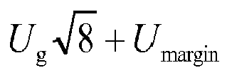
- the predetermined voltage threshold may be: U g ⁇ 8 + U margin
- the controllable switch S Y is controlled to be non-conductive when the impedance Z DC between the positive direct current pole U DC,P or negative direct current pole U DC,N and the earth potential of the alternating current network supplied by the inverter is higher than a predetermined threshold, and the controllable switch S Y is controlled to be conductive when the impedance Z DC between the positive U DC,P or negative direct current pole U DC,N and the earth potential of the alternating current network supplied by the inverter is lower than the predetermined threshold.
- the predetermined impedance threshold may correspond to a value for the impedance Z DC that is high enough for a low-frequency leakage current not to flow to a harmful degree.
- the impedance condition may be given a priority.
- first controllable switch S X connected between the neutral direct current pole M of the inverter and a virtual neutral point of an alternating current network supplied by the inverter and a second controllable switch S Y connected between the neutral direct current pole M of the inverter and the earth potential of the alternating current network supplied by the inverter.
- the first switch S X and the second switch S Y are controlled according to one or more predetermined parameters. This may be implemented with a control arrangement 20 which is configured to control the switches according to the one or more predetermined parameters.
- the one or more predetermined parameters may comprise one or more voltage parameters and/or one or more impedance parameters.
- the first controllable switch S X is controlled to be non-conductive when the voltage U DC between the positive direct current pole U DC,P and the negative direct current pole U DC,N is lower than a first predetermined threshold or higher than a second predetermined threshold, and the first controllable switch S X is controlled to be conductive when the voltage U DC between the positive direct current pole U DC,P and the negative direct current pole U DC,N is higher than the first predetermined threshold and lower than the second predetermined threshold.
- the second controllable switch S Y is controlled to be non-conductive when the voltage U DC between the positive direct current pole U DC,P and the negative direct current pole U DC,N is lower than the second predetermined threshold, and the second controllable switch S Y is controlled to be conductive when the voltage U DC between the positive direct current pole U DC,P and the negative direct current pole U DC,N is higher than the second predetermined threshold.
- the value of the voltage U DC used in the control may be a reference value of the voltage U DC or a measured value of the voltage U DC .
- U margin and U add depend on system properties.
- Table 1 below shows the conditions of control according to an embodiment: State S x S y Basic Condition S x S y Off Off U DC ⁇ U limit,1 S x S y On Off U limit,1 ⁇ U DC ⁇ U limit,2 S x S y Off On U DC ⁇ U limit,2 S x S y On On None permitted
- state SxSy When transiting from state Sx S y to state SxSy or from state SxSy to state Sx S y, it is preferable to proceed via state SxSy as state SxSy is preferably avoided.
- the first controllable switch S X is controlled to be non-conductive when the impedance Z DC between the positive direct current pole U DC,P or negative direct current pole U DC,N and the earth potential of the alternating current network supplied by the inverter is higher than a first predetermined threshold or lower than a second predetermined threshold, and the first controllable switch S X is controlled to be conductive when the impedance Z DC between the positive U DC,P or negative direct current pole U DC,N and the earth potential of the alternating current network supplied by the inverter is lower than the first predetermined threshold and higher than the second predetermined threshold.
- the second controllable switch S Y is controlled to be non-conductive when the impedance Z DC between the positive direct current pole U DC,P or negative direct current pole U DC,N and the earth potential of the alternating current network supplied by the inverter is higher than the second predetermined threshold, and the controllable switch S Y is controlled to be conductive when the impedance Z DC between the positive U DC,P or negative direct current pole U DC,N and the earth potential of the alternating current network supplied by the inverter is lower than the second predetermined threshold.
- the first predetermined impedance threshold Z limit,1 may correspond to a value for the impedance Z DC that is high enough for a high-frequency leakage current not to flow to a harmful degree.
- the second predetermined impedance threshold Z limit,2 may correspond to a value for the impedance Z DC that is high enough for a low-frequency leakage current not to flow to a harmful degree.
- Z limit,1 > Z limit,2 .
- Table 2 below shows the conditions of control according to an embodiment: State S x S y Basic Condition S x S y Off Off Z DC > Z limit,1 S x S y On Off Z limit,2 ⁇ Z DC ⁇ Z limit,1 S x S y Off On Z DC ⁇ Z limit,2 S x S y On On None permitted
- state SxSy When transiting from state Sx S y to state SxSy or from state SxSy to state Sx S y, it is preferable to proceed via state SxSy as state SxSy is preferably avoided.
- the impedance condition may be given a priority.
- the first controllable switch S X and/or the second controllable switch S Y in the above embodiments may, alternatively or in addition, be controlled according to an output current of the inverter (or an output power of the inverter).
- the first controllable switch S X and/or the second controllable switch S Y may be controlled such that the output current of the inverter is maximized and common-mode voltages are mitigated when the conditions allow.
- the conditions and thresholds possibly used in connection with this embodiment depend on the particular system.
- control of the controllable switch(es) S X , S Y can be performed manually or by or via the control arrangement 20, which can also perform the normal modulation control of the semiconductor switches of the inverter. It is also possible to use additional or separate logical or physical units (not shown) for performing the control functionality of the invention.
- the functionality of the invention could, for example, be implemented using a separate logic arrangement, which could be independent of the normal modulation control of the semiconductor switches of the inverter, for example.
- the control arrangement 20 and/or a separate logic arrangement controlling the controllable semiconductor switches according to any one of the above embodiments, or a combination thereof, can be implemented as one unit or as two or more separate units that are configured to implement the functionality of the various embodiments.
- the term 'unit' refers generally to a physical or logical entity, such as a physical device or a part thereof or a software routine.
- the control arrangement 20 according to any one of the embodiments may be implemented at least partly by means of one or more computers or corresponding digital signal processing (DSP) equipment provided with suitable software, for example.
- DSP digital signal processing
- Such a computer or digital signal processing equipment preferably comprises at least a working memory (RAM) providing storage area for arithmetical operations, and a central processing unit (CPU), such as a general-purpose digital signal processor.
- the CPU may comprise a set of registers, an arithmetic logic unit, and a CPU control unit.
- the CPU control unit is controlled by a sequence of program instructions transferred to the CPU from the RAM.
- the CPU control unit may contain a number of microinstructions for basic operations. The implementation of microinstructions may vary depending on the CPU design.
- the program instructions may be coded by a programming language, which may be a high-level programming language, such as C, Java, etc., or a low-level programming language, such as a machine language, or an assembler.
- the computer may also have an operating system which may provide system services to a computer program written with the program instructions.
- the computer or other apparatus implementing the invention, or a part thereof, may further comprise suitable input means for receiving e.g. measurement and/or control data, and output means for outputting e.g. control data.
- PLD programmable logic devices
- FPGA field-programmable gate array
- the control arrangement 20 according to any one of the embodiments may be implemented at least partly by means of such analog circuits or programmable logic devices.
- the invention can be implemented in existing system elements or by using separate dedicated elements or devices in a centralized or distributed manner.
- Present inverters can comprise programmable logic devices or processors and memory that can be utilized in the functions according to embodiments of the invention.
- all modifications and configurations required for implementing an embodiment of the invention e.g. in existing inverters may be performed as software routines, which may be implemented as added or updated software routines.
- software can be provided as a computer program product comprising computer program code which, when run on a computer, causes the computer or a corresponding arrangement to perform the functionality according to the invention as described above.
- Such a computer program code may be stored or generally embodied on a computer readable medium, such as a suitable memory, e.g. a flash memory or an optical memory, from which it is loadable to the unit or units executing the program code.
- a computer program code implementing the invention may be loaded to the unit or units executing the computer program code via a suitable data network, for example, and it may replace or update a possibly existing program code.
Abstract
Description
- The invention relates to a switching arrangement for an inverter, an inverter, and a method for controlling an inverter.
- Some converters, such as inverters or rectifiers, may have three DC poles. In addition to positive and negative DC poles, they have a neutral DC pole. For example, three-level converters have three DC poles. Examples of three-level converters are given in T. Brückner, S. Bernet and H. Güldner, "The Active NPC Converter and Its Loss-Balancing Control", IEEE Transactions on Industrial Electronics, Vol. 52, No. 3, June 2005. In particular, examples of three-level neutral-point-clamped (NPC) converters are given.
-
Figure 1 shows an example of a main circuit of a three-level inverter. The inverter may be supplied by one or morephotovoltaic panels 10 connected between its positive and negative direct current poles UDC,P, UDC,N as illustrated in the example. The inverter further supplies a three phase power system connected to its alternating current poles AC1, AC2, AC3. - A possible problem related to the use of three-level inverters is that in normal operation a high-frequency voltage is formed between the DC circuit and earth, i.e. a common-mode voltage ucm includes a high-frequency component. This high-frequency component may stress, e.g. in case of photovoltaic applications, insulations of the photovoltaic panels and further cause harmful high-frequency currents in the vicinity of support structures of the photovoltaic panels. The following equation applies to the system of
Figure 1 :
where
Ug = phase voltage of the three phase power system supplied by the inverter
Umargin = voltage value depending on the system control and component values - The formation of the common-mode voltage ucm may be prevented by earthing the neutral direct current pole M of the inverter DC circuit as illustrated in
Figure 2 . This solution eliminates the common-mode voltage ucm completely and thus also the voltages of the positive and negative direct current poles UDC,P, UDC,N against earth are pure DC voltages; in this case UPM and UMN respectively. A possible problem related to this solution is that the voltage UDC of the DC circuit must be considerably higher. The following equation applies to the system ofFigure 2 :
- Since typically only the high-frequency components of the common-mode voltage ucm cause problems, it may be enough to only remove these components. This may be accomplished by connecting the neutral direct current pole M of the inverter DC circuit to a virtual neutral point of the power system supplied by the inverter. The virtual neutral point of a three phase power system generally refers to a star point of three star-connected impedances in the three-phase power system. An example of such a virtual neutral point is the star point of star-connected capacitors of an AC output filter of the inverter as shown in
Figure 3 . This procedure is also called virtual earthing. The virtual earthing makes the operation possible with a lower voltage UDC of the DC circuit than in the case of an earthed system (as inFigure 2 ). However, a possible problem with this solution, when compared with the system ofFigure 1 , is that e.g. the current stress of the semiconductor switches is greater and the operation requires a higher voltage UDC of the DC circuit. The following equation applies to the system ofFigure 3 :
where
Uadd = additional voltage depending on the system control and modulation methods and component values - In practice Uadd may be about 20 to 50 V, which is 5 to 12% if a desirable voltage variation of a maximum power point tracking of the inverter is 400 V. This 5 to 12% in the DC voltage range may be a significant amount when possible operating environments of the system are evaluated.
- An object of the invention is to provide a method and an apparatus so as to solve or at least alleviate the above problems. The object of the invention is achieved by a switching arrangement, an inverter, a method, and a computer program product that are characterized by what is stated in the independent claims. Preferred embodiments of the invention are described in the dependent claims.
- The invention is based on the idea of providing a controllable switch connected between the neutral direct current pole of the inverter and the virtual neutral point of the alternating current network supplied by the inverter. Alternatively or in addition to this, the invention is based on the idea of providing a controllable switch connected between the neutral direct current pole of the inverter and the earth potential of an alternating current network supplied by the inverter.
- The solution of the invention provides the advantage that the neutral direct current pole of the inverter may be connected to or disconnected from the virtual neutral point of the alternating current network supplied by the inverter and/or the earth potential of an alternating current network supplied by the inverter, depending on what the most optimal mode of operation in the operating point and application in question is. The invention enables maximization of energy production and, generally, optimization of efficiency of inverter applications.
- The invention will now be explained in greater detail in connection with preferred embodiments and with reference to the attached drawings, in which:
-
Figure 1 shows a circuit diagram of a three-phase three-level inverter according to an embodiment; -
Figure 2 shows a circuit diagram of a three-phase three-level inverter according to an embodiment; -
Figure 3 shows a circuit diagram of a three-phase three-level inverter according to an embodiment; -
Figure 4 shows a circuit diagram of a three-phase three-level inverter according to an embodiment; -
Figure 5 shows a circuit diagram of a three-phase three-level inverter according to an embodiment; and -
Figure 6 shows a circuit diagram of a three-phase three-level inverter according to an embodiment. - The application of the invention is not restricted to any specific system, but it may be applied to various electric systems. In addition, the use of the invention is not restricted to any system utilizing a specific basic frequency or to any specific voltage level. While the following examples relate to three-phase three-level inverters, the invention may be applied to any inverter, such as a two-level inverter, that has three DC poles, namely a positive direct current pole, a negative direct current pole, and a neutral direct current pole. In addition, the invention may also be applied to two-phase inverters or inverters having more than three phases, for example.
-
Figure 4 shows a circuit diagram of a three-phase three-level inverter in accordance with an embodiment. It should be noted that the figure only presents elements essential to the understanding of the invention. The three-phase three-level inverter comprises a positive direct current pole UDC,P, a negative direct current pole UDC,N, a neutral direct current pole M, and three switching branches, each switching branch comprising four controllable semiconductor switches connected in series between the positive direct current pole and the negative direct current pole. More specifically, each switching branch of the three-phase three-level inverter comprises an alternating current pole AC1, AC2, AC3 and a first controllable semiconductor switch S1, S5, S9 and a second controllable semiconductor switch S2, S6, S10 connected in series between the positive direct current pole UDC,P and the alternating current pole AC1, AC2, AC3 of the switching branch, wherein the first controllable semiconductor switch S1, S5, S9 is connected to the positive direct current pole UDC,P. A first diode D1, D5, D9 may be connected in parallel to the first controllable semiconductor switch S1, S5, S9 and a second diode D2, D6, D10 may be connected in parallel to the second controllable semiconductor switch S2, S6, S10. Further, each switching branch comprises a third controllable semiconductor switch S3, S7, S11 and a fourth controllable semiconductor switch S4, S8, S12 connected in series between the negative direct current pole UDC,N and the alternating current pole AC1, AC2, AC3 of the switching branch, wherein the fourth controllable semiconductor switch S4, S8, S12 is connected to the negative direct current pole UDC,N. A third diode D3, D7, D11 may be connected in parallel to the third controllable semiconductor switch S3, S7, S11, and a fourth diode D4, D8, D12 may be connected in parallel to the fourth controllable semiconductor switch S4, S8, S12. Further, each switching branch comprises a fifth diode D13, D15, D17 connected between the neutral direct current pole M and a connection point between the first controllable semiconductor switch S1, S5, S9 and the second controllable semiconductor switch S2, S6, S10, and a sixth diode D14, D16, D18 connected between the neutral direct current pole M and a connection point between the third controllable semiconductor switch S3, S7, S11 and the fourth controllable semiconductor switch S4, S8, S12. The controllable semiconductor switches can be IGBTs (Insulated Gate Bipolar Transistor) or FETs (Field-Effect Transistor) or any corresponding controllable semiconductor switches. For the sake of clarity,Figure 4 does not show any control connections via which the controllable semiconductor switches S1 to S12 are controlled. The control of the semiconductor switches S1 to S12 can involve one or more control components (not shown). While the inverter of the example ofFigure 4 is a neutral-point-clamped inverter, the inverter could be an active neutral-point-clamped inverter, for example, or another type of three-level inverter. -
Figure 4 further shows an example of a DC intermediate circuit of the exemplary inverter, which DC intermediate circuit may comprise capacitors CDC,P and CDC,N as illustrated. The structure of the intermediate circuit could also be different, depending on the circuit configuration used. The exemplary inverter ofFigure 4 may be supplied by one or morephotovoltaic panels 10 connected between its positive and negative direct current poles UDC,P, UDC,N as illustrated in the example. The inverter may also be supplied from another kind of source. The exemplary inverter ofFigure 4 may supply a three-phase alternating current network through its alternating current poles AC1, AC2, AC3. There may be an output filter connected to the alternating current poles AC1, AC2, AC3 of the inverter. The output filter may be an LC or LCL type of filter, for example.Figure 4 illustrates an LC type output filter with three inductances LC1, LC2, LC3 and three star-connected capacitances C1, C2, C3. The rest of the three-phase alternating current network is shown inFigure 4 in a simplified manner, with three inductances Lg1, Lg2, Lg3 and three phase voltages Ug1, Ug2, Ug3. - According to an embodiment, as shown in
Figure 4 , there is a controllable switch SX connected between the neutral direct current pole M of the inverter and a virtual neutral point of an alternating current network supplied by the inverter. An example of such a virtual neutral point in a three-phase system is the star point of the star-connected capacitors of the AC output filter of the inverter as shown in the example ofFigure 4 . However, the virtual neutral point of the three-phase alternating current network supplied by the inverter generally refers to any star point of three star-connected impedances, such as capacitors or resistors or a combination thereof, in the three-phase alternating current network supplied by the inverter. In a two-phase system, such a virtual neutral point may be a connection point of two impedances, such as capacitors or resistors or a combination thereof, connected in series between the phases. The controllable switch SX may be part of the inverter or part of a separate switching arrangement, for example. The controllable switch SX may be an electromechanical switch, such as a relay or a contactor, or a semiconductor switch, for example. The controllable switch SX may also be a manually controllable mechanical switch. - According to an embodiment, the switch SX is controlled according to one or more predetermined parameters. This may be performed manually by an operator of the inverter system. Such a manual control of the switch SX may take place at any time. The switch SX may be set at the start-up of the inverter system or later according to the one or more predetermined parameters, such as system conditions, and the setting may be changed if necessary. The control of the switch SX may also be performed automatically. For this, a
control arrangement 20 may be provided which is configured to control the switch SX according to the one or more predetermined parameters. Also thecontrol arrangement 20 or a corresponding entity may be part of the inverter or part of a separate switching arrangement, for example. According to an embodiment, the one or more predetermined parameters may comprise one or more voltage parameters and/or one or more impedance parameters. Thecontrol arrangement 20 or a corresponding entity may comprise or may be connected to a suitable measuring arrangement (not shown) which can measure voltage and/or impedance values possibly needed in the various embodiments. Examples of such voltage and impedance values include a voltage UDC between the positive direct current pole UDC,P and the negative direct current pole UDC,N, and an impedance ZDC between the positive direct current pole UDC,P or negative direct current pole UDC,N and the earth potential of the alternating current network supplied by the inverter. - According to an embodiment, the controllable switch SX is controlled to be non-conductive (OFF state) when the voltage UDC between the positive direct current pole UDC,P and the negative direct current pole UDC,N is lower than a predetermined threshold, and the controllable switch SX is controlled to be conductive (ON state) when the voltage UDC between the positive direct current pole UDC,P and the negative direct current pole UDC,N is higher than the predetermined threshold. The value of the voltage UDC used in the control may be a reference value of the voltage UDC or a measured value of the voltage UDC. According to an embodiment, the predetermined voltage threshold may be:

where
Ug = phase voltage of the alternating current network supplied by the inverter
Umargin = voltage value depending on the system control and component values
Uadd = additional voltage depending on the system control and modulation methods and component values - According to an embodiment, the controllable switch SX is controlled to be non-conductive when the impedance ZDC between the positive direct current pole UDC,P or negative direct current pole UDC,N and the earth potential of the alternating current network supplied by the inverter is higher than a predetermined threshold, and the controllable switch SX is controlled to be conductive when the impedance ZDC between the positive UDC,P or negative direct current pole UDC,N and the earth potential of the alternating current network supplied by the inverter is lower than the predetermined threshold. According to an embodiment, the predetermined impedance threshold may correspond to a value for the impedance ZDC that is high enough for a high-frequency leakage current not to flow to a harmful degree.
- It is also possible to combine the voltage-based and impedance-based controls described above and use them simultaneously. In such a case, the impedance condition may be given priority.
- According to an embodiment, as shown in
Figure 5 , there is a controllable switch SY connected between the neutral direct current pole M of the inverter and the earth potential of the alternating current network supplied by the inverter. The controllable switch SY may be part of the inverter or part of a separate switching arrangement, for example. The controllable switch SY may be an electromechanical switch, such as a relay or a contactor, or a semiconductor switch, for example. The controllable switch SY may also be a manually controllable mechanical switch. - According to an embodiment, the switch SY is controlled according to one or more predetermined parameters. This may be performed manually by an operator of the inverter system. Such a manual control of the switch SY may take place at any time. The switch SY may be set at the start-up of the inverter system or later according to the one or more predetermined parameters, such as system conditions, and the setting may be changed if necessary. The control of the switch SY may also be performed automatically. For this, a
control arrangement 20 may be provided which is configured to control the switch SY according to the one or more predetermined parameters. Also thecontrol arrangement 20 or a corresponding entity may be part of the inverter or part of a separate switching arrangement, for example. According to an embodiment, the one or more predetermined parameters may comprise one or more voltage parameters and/or one or more impedance parameters. - According to an embodiment, the controllable switch SY is controlled to be non-conductive (OFF state) when the voltage UDC between the positive direct current pole UDC,P and the negative direct current pole UDC,N is lower than a predetermined threshold, and the controllable switch SY is controlled to be conductive (ON state) when the voltage UDC between the positive direct current pole UDC,P and the negative direct current pole UDC,N is higher than the predetermined threshold. The value of the voltage UDC used in the control may be a reference value of the voltage UDC or a measured value of the voltage UDC. According to an embodiment, the predetermined voltage threshold may be:
- According to an embodiment, the controllable switch SY is controlled to be non-conductive when the impedance ZDC between the positive direct current pole UDC,P or negative direct current pole UDC,N and the earth potential of the alternating current network supplied by the inverter is higher than a predetermined threshold, and the controllable switch SY is controlled to be conductive when the impedance ZDC between the positive UDC,P or negative direct current pole UDC,N and the earth potential of the alternating current network supplied by the inverter is lower than the predetermined threshold. According to an embodiment, the predetermined impedance threshold may correspond to a value for the impedance ZDC that is high enough for a low-frequency leakage current not to flow to a harmful degree.
- It is also possible to combine the voltage-based and impedance-based controls described above and use them simultaneously. In such a case, the impedance condition may be given a priority.
- According to an embodiment, as shown in
Figure 6 , there is a first controllable switch SX connected between the neutral direct current pole M of the inverter and a virtual neutral point of an alternating current network supplied by the inverter and a second controllable switch SY connected between the neutral direct current pole M of the inverter and the earth potential of the alternating current network supplied by the inverter. Further, according to an embodiment, the first switch SX and the second switch SY are controlled according to one or more predetermined parameters. This may be implemented with acontrol arrangement 20 which is configured to control the switches according to the one or more predetermined parameters. According to an embodiment, the one or more predetermined parameters may comprise one or more voltage parameters and/or one or more impedance parameters. - According to an embodiment, the first controllable switch SX is controlled to be non-conductive when the voltage UDC between the positive direct current pole UDC,P and the negative direct current pole UDC,N is lower than a first predetermined threshold or higher than a second predetermined threshold, and the first controllable switch SX is controlled to be conductive when the voltage UDC between the positive direct current pole UDC,P and the negative direct current pole UDC,N is higher than the first predetermined threshold and lower than the second predetermined threshold. In addition, the second controllable switch SY is controlled to be non-conductive when the voltage UDC between the positive direct current pole UDC,P and the negative direct current pole UDC,N is lower than the second predetermined threshold, and the second controllable switch SY is controlled to be conductive when the voltage UDC between the positive direct current pole UDC,P and the negative direct current pole UDC,N is higher than the second predetermined threshold. The value of the voltage UDC used in the control may be a reference value of the voltage UDC or a measured value of the voltage UDC.
- According to an embodiment, the first predetermined voltage threshold may be:

and the second predetermined voltage threshold may be:
- As noted already above in connection with other embodiments, the values of Umargin and Uadd depend on system properties. According to an embodiment, U add ≈ (U limit,2 - U limit,1)/2.
Table 1 below shows the conditions of control according to an embodiment: State Sx Sy Basic Condition S x S y Off Off U DC< U limit,1 Sx S y On Off U limit,1 ≤ U DC < U limit,2 S xSy Off On U DC ≥ U limit,2 SxSy On On Never permitted - When transiting from state SxSy to state SxSy or from state SxSy to state SxSy, it is preferable to proceed via state SxSy as state SxSy is preferably avoided.
- According to an embodiment, the first controllable switch SX is controlled to be non-conductive when the impedance ZDC between the positive direct current pole UDC,P or negative direct current pole UDC,N and the earth potential of the alternating current network supplied by the inverter is higher than a first predetermined threshold or lower than a second predetermined threshold, and the first controllable switch SX is controlled to be conductive when the impedance ZDC between the positive UDC,P or negative direct current pole UDC,N and the earth potential of the alternating current network supplied by the inverter is lower than the first predetermined threshold and higher than the second predetermined threshold. In addition, the second controllable switch SY is controlled to be non-conductive when the impedance ZDC between the positive direct current pole UDC,P or negative direct current pole UDC,N and the earth potential of the alternating current network supplied by the inverter is higher than the second predetermined threshold, and the controllable switch SY is controlled to be conductive when the impedance ZDC between the positive UDC,P or negative direct current pole UDC,N and the earth potential of the alternating current network supplied by the inverter is lower than the second predetermined threshold. According to an embodiment, the first predetermined impedance threshold Zlimit,1 may correspond to a value for the impedance ZDC that is high enough for a high-frequency leakage current not to flow to a harmful degree. According to an embodiment, the second predetermined impedance threshold Zlimit,2 may correspond to a value for the impedance ZDC that is high enough for a low-frequency leakage current not to flow to a harmful degree. In addition, Zlimit,1 > Zlimit,2.
Table 2 below shows the conditions of control according to an embodiment: State Sx Sy Basic Condition S x S y Off Off ZDC > Z limit,1 Sx S y On Off Zlimit,2 ≤ ZDC ≤ Zlimit,1 S xSy Off On ZDC < Zlimit,2 SxSy On On Never permitted - When transiting from state SxSy to state SxSy or from state SxSy to state SxSy, it is preferable to proceed via state SxSy as state SxSy is preferably avoided.
- It is also possible to combine the voltage-based and impedance-based controls described above and use them simultaneously. In such a case, the impedance condition may be given a priority.
- According to an embodiment, the first controllable switch SX and/or the second controllable switch SY in the above embodiments may, alternatively or in addition, be controlled according to an output current of the inverter (or an output power of the inverter). For example, the first controllable switch SX and/or the second controllable switch SY may be controlled such that the output current of the inverter is maximized and common-mode voltages are mitigated when the conditions allow. The conditions and thresholds possibly used in connection with this embodiment depend on the particular system.
- The control of the controllable switch(es) SX, SY according to the various embodiments described above can be performed manually or by or via the
control arrangement 20, which can also perform the normal modulation control of the semiconductor switches of the inverter. It is also possible to use additional or separate logical or physical units (not shown) for performing the control functionality of the invention. The functionality of the invention could, for example, be implemented using a separate logic arrangement, which could be independent of the normal modulation control of the semiconductor switches of the inverter, for example. - The
control arrangement 20 and/or a separate logic arrangement controlling the controllable semiconductor switches according to any one of the above embodiments, or a combination thereof, can be implemented as one unit or as two or more separate units that are configured to implement the functionality of the various embodiments. Here the term 'unit' refers generally to a physical or logical entity, such as a physical device or a part thereof or a software routine. Thecontrol arrangement 20 according to any one of the embodiments may be implemented at least partly by means of one or more computers or corresponding digital signal processing (DSP) equipment provided with suitable software, for example. Such a computer or digital signal processing equipment preferably comprises at least a working memory (RAM) providing storage area for arithmetical operations, and a central processing unit (CPU), such as a general-purpose digital signal processor. The CPU may comprise a set of registers, an arithmetic logic unit, and a CPU control unit. The CPU control unit is controlled by a sequence of program instructions transferred to the CPU from the RAM. The CPU control unit may contain a number of microinstructions for basic operations. The implementation of microinstructions may vary depending on the CPU design. The program instructions may be coded by a programming language, which may be a high-level programming language, such as C, Java, etc., or a low-level programming language, such as a machine language, or an assembler. The computer may also have an operating system which may provide system services to a computer program written with the program instructions. The computer or other apparatus implementing the invention, or a part thereof, may further comprise suitable input means for receiving e.g. measurement and/or control data, and output means for outputting e.g. control data. It is also possible to use analog circuits, programmable logic devices (PLD), such as a field-programmable gate array (FPGA), or discrete electric components and devices for implementing the functionality according to any one of the embodiments. For example, thecontrol arrangement 20 according to any one of the embodiments may be implemented at least partly by means of such analog circuits or programmable logic devices. - The invention can be implemented in existing system elements or by using separate dedicated elements or devices in a centralized or distributed manner. Present inverters, for example, can comprise programmable logic devices or processors and memory that can be utilized in the functions according to embodiments of the invention. Thus, all modifications and configurations required for implementing an embodiment of the invention e.g. in existing inverters may be performed as software routines, which may be implemented as added or updated software routines. If at least part of the functionality of the invention is implemented by software, such software can be provided as a computer program product comprising computer program code which, when run on a computer, causes the computer or a corresponding arrangement to perform the functionality according to the invention as described above. Such a computer program code may be stored or generally embodied on a computer readable medium, such as a suitable memory, e.g. a flash memory or an optical memory, from which it is loadable to the unit or units executing the program code. In addition, such a computer program code implementing the invention may be loaded to the unit or units executing the computer program code via a suitable data network, for example, and it may replace or update a possibly existing program code.
- It is obvious to a person skilled in the art that, as technology advances, the basic idea of the invention may be implemented in various ways. The invention and its embodiments are thus not restricted to the above examples but may vary within the scope of the claims.
Claims (15)
- A switching arrangement for an inverter, the inverter comprising a positive direct current pole (UDC,P), a negative direct current pole (UDC,N), and a neutral direct current pole (M), characterized in that the arrangement comprises:a) a first controllable switch (SX) connected between the neutral direct current pole (M) of the inverter and a virtual neutral point of an alternating current network supplied by the inverter;
and/orb) a second controllable switch (SY) connected between the neutral direct current pole (M) of the inverter and an earth potential of an alternating current network supplied by the inverter. - An arrangement according to claim 1, characterized in that, as per alternative a), the virtual neutral point of the alternating current network supplied by the inverter is a star point of three star-connected impedances in the alternating current network.
- An arrangement according to claim 1 or 2, characterized in that, as per alternative a), the arrangement comprises means (20) for controlling the first controllable switch (SX) configured to control the first controllable switch according to one or more predetermined parameters;
and/or
as per alternative b), the arrangement comprises means (20) for controlling the second controllable switch (SY) configured to control the second controllable switch according to one or more predetermined parameters. - An arrangement according to claim 3, characterized in that the one or more predetermined parameters comprise one or more voltage parameters and/or one or more impedance parameters and/or one or more current parameters and/or one or more power parameters.
- An arrangement according to claim 4, characterized in that when the arrangement comprises only the first controllable switch (SX), the means for controlling the first controllable switch are configured to:control the first controllable switch (SX) to be non-conductive when a voltage between the positive direct current pole (UDC,P) and the negative direct current pole (UDC,N) is lower than a predetermined threshold; andcontrol the first controllable switch (SX) to be conductive when the voltage between the positive direct current pole (UDC,P) and the negative direct current pole (UDC,N) is higher than the predetermined threshold.
- An arrangement according to claim 4, characterized in that when the arrangement comprises only the second controllable switch (SY), the means for controlling the second controllable switch are configured to:control the second controllable switch (SY) to be non-conductive when a voltage between the positive direct current pole (UDC,P) and the negative direct current pole (UDC,N) is lower than a predetermined threshold; andcontrol the second controllable switch (SY) to be conductive when the voltage between the positive direct current pole (UDC,P) and the negative direct current pole (UDC,N) is higher than the predetermined threshold.
- An arrangement according to claim 4, characterized in that when the arrangement comprises both the first controllable switch (SX) and the second controllable switch (SY),
the means for controlling the first controllable switch (SX) are configured to:control the first controllable switch (SX) to be non-conductive when a voltage between the positive direct current pole (UDC,P) and the negative direct current pole (UDC,N) is lower than a first predetermined threshold or higher than a second predetermined threshold; andcontrol the first controllable switch (SX) to be conductive when the voltage between the positive direct current pole (UDC,P) and the negative direct current pole (UDC,N) is higher than the first predetermined threshold and lower than the second predetermined threshold; andthe means for controlling the second controllable switch (SY) are configured to:control the second controllable switch (SY) to be non-conductive when the voltage between the positive direct current pole (UDC,P) and the negative direct current pole (UDC,N) is lower than the second predetermined threshold; andcontrol the second controllable switch (SY) to be conductive when the voltage between the positive direct current pole (UDC,P) and the negative direct current pole (UDC,N) is higher than the second predetermined threshold. - An arrangement according to claim 4, characterized in that when the arrangement comprises only the first controllable switch (SX), the means for controlling the first controllable switch are configured to:control the first controllable switch (SX) to be non-conductive when an impedance between the positive or negative direct current pole and the earth potential of the alternating current network supplied by the inverter is higher than a predetermined threshold; andcontrol the first controllable switch (SX) to be conductive when the impedance between the positive or negative direct current pole and the earth potential of the alternating current network supplied by the inverter is lower than the predetermined threshold.
- An arrangement according to claim 4, characterized in that when the arrangement comprises only the second controllable switch (SY), the means for controlling the second controllable switch are configured to:control the second controllable switch (SY) to be non-conductive when an impedance between the positive or negative direct current pole and the earth potential of the alternating current network supplied by the inverter is higher than a predetermined threshold; andcontrol the second controllable switch (SY) to be conductive when the impedance between the positive or negative direct current pole and the earth potential of the alternating current network supplied by the inverter is lower than the predetermined threshold.
- An arrangement according to claim 4, characterized in that when the arrangement comprises both the first controllable switch (SX) and the second controllable switch (SY),
the means for controlling the first controllable switch (SX) are configured to:control the first controllable switch (SX) to be non-conductive when an impedance between the positive or negative direct current pole and the earth potential of the alternating current network supplied by the inverter is higher than a first predetermined threshold or lower than a second predetermined threshold; andcontrol the first controllable switch (SX) to be conductive when the impedance between the positive or negative direct current pole and the earth potential of the alternating current network supplied by the inverter is lower than the first predetermined threshold and higher than the second predetermined threshold; andthe means for controlling the second controllable switch (SY) are configured to:control the second controllable switch (SY) to be non-conductive when the impedance between the positive or negative direct current pole and the earth potential of the alternating current network supplied by the inverter is higher than the second predetermined threshold; andcontrol the second controllable switch (SY) to be conductive when the impedance between the positive or negative direct current pole and the earth potential of the alternating current network supplied by the inverter is lower than the second predetermined threshold. - An inverter comprising a positive direct current pole (UDC,P), a negative direct current pole (UDC,N), and a neutral direct current pole (M), characterized in that the inverter comprises an arrangement according to any one of claims 1 to 10.
- An inverter according to claim 11, characterized in that the inverter is a three-phase three-level inverter comprising three switching branches, wherein each switching branch comprises four controllable semiconductor switches (S1, S2, S3, S4; S5, S6, S7, S8; S9, S10, S11, S12) connected in series between the positive direct current pole and the negative direct current pole.
- An inverter according to claim 12, characterized in that the inverter is a neutral-point-clamped inverter or an active neutral-point-clamped inverter.
- A method for controlling an inverter, the inverter comprising a positive direct current pole (UDC,P), a negative direct current pole (UDC,N), and a neutral direct current pole (M), characterized in thata) the inverter comprises a first controllable switch (SX) connected between the neutral direct current pole (M) of the inverter and a virtual neutral point of an alternating current network supplied by the inverter, wherein the method comprises controlling the first controllable switch according to one or more predetermined parameters;
and/orb) the inverter comprises a second controllable switch (SY) connected between the neutral direct current pole (M) of the inverter and an earth potential of an alternating current network supplied by the inverter, wherein the method comprises controlling the second controllable switch according to one or more predetermined parameters. - A computer program product comprising computer program code, wherein execution of the program code on a computer causes the computer to carry out the steps of the method according to claim 14.
Priority Applications (4)
| Application Number | Priority Date | Filing Date | Title |
|---|---|---|---|
| ES13166951T ES2730851T3 (en) | 2013-05-08 | 2013-05-08 | Switching arrangement for inverter and inverter |
| EP13166951.7A EP2802054B1 (en) | 2013-05-08 | 2013-05-08 | Switching arrangement for inverter, and inverter |
| CN201410189311.7A CN104143931B (en) | 2013-05-08 | 2014-05-06 | Switchgear, inverter and the method for control inverter for inverter |
| US14/271,891 US9172311B2 (en) | 2013-05-08 | 2014-05-07 | Switching arrangement for inverter, and inverter |
Applications Claiming Priority (1)
| Application Number | Priority Date | Filing Date | Title |
|---|---|---|---|
| EP13166951.7A EP2802054B1 (en) | 2013-05-08 | 2013-05-08 | Switching arrangement for inverter, and inverter |
Publications (3)
| Publication Number | Publication Date |
|---|---|
| EP2802054A1 true EP2802054A1 (en) | 2014-11-12 |
| EP2802054A9 EP2802054A9 (en) | 2015-06-24 |
| EP2802054B1 EP2802054B1 (en) | 2019-03-27 |
Family
ID=48325461
Family Applications (1)
| Application Number | Title | Priority Date | Filing Date |
|---|---|---|---|
| EP13166951.7A Not-in-force EP2802054B1 (en) | 2013-05-08 | 2013-05-08 | Switching arrangement for inverter, and inverter |
Country Status (4)
| Country | Link |
|---|---|
| US (1) | US9172311B2 (en) |
| EP (1) | EP2802054B1 (en) |
| CN (1) | CN104143931B (en) |
| ES (1) | ES2730851T3 (en) |
Cited By (2)
| Publication number | Priority date | Publication date | Assignee | Title |
|---|---|---|---|---|
| WO2015074965A1 (en) * | 2013-11-25 | 2015-05-28 | Sma Solar Technology Ag | Method for operating an inverter and inverter comprising a switch between a center point of a dc link and a connection for a pen conductor of an ac grid |
| WO2021148617A1 (en) * | 2020-01-24 | 2021-07-29 | Bucher Hydraulics Ag | Power converter, charging post and vehicle |
Families Citing this family (7)
| Publication number | Priority date | Publication date | Assignee | Title |
|---|---|---|---|---|
| EP3002867B1 (en) * | 2014-10-01 | 2019-12-04 | ABB Schweiz AG | Three-level converter and method for controlling three-level converter |
| CN107204703A (en) * | 2016-03-17 | 2017-09-26 | 中国航空工业集团公司雷华电子技术研究所 | A kind of anti-voltage surge method for three-phase three-switch three-level circuit |
| DE102016207941A1 (en) * | 2016-05-09 | 2017-11-09 | Fraunhofer-Gesellschaft zur Förderung der angewandten Forschung e.V. | A device for generating an alternating voltage, circuit arrangement for generating an AC output voltage, method for generating an AC output voltage, inverter for generating an AC voltage from a DC voltage, energy storage device for providing an AC voltage using a DC energy storage, three-phase inverter device, three-phase inverter circuit, and concept for generating a DC voltage |
| US9917543B1 (en) * | 2016-10-19 | 2018-03-13 | Wisconsin Alumni Research Foundation | Inverter for common mode voltage cancellation |
| US10103663B1 (en) * | 2017-04-18 | 2018-10-16 | General Electric Company | Control method for protecting switching devices in power converters in doubly fed induction generator power systems |
| CN111146851A (en) * | 2020-03-12 | 2020-05-12 | 深圳威迈斯新能源股份有限公司 | Single three-phase compatible conversion circuit and vehicle-mounted charger |
| CN111490525A (en) * | 2020-03-19 | 2020-08-04 | 国网江苏省电力有限公司盐城供电分公司 | Open-phase detection and fault-tolerant control method for three-phase photovoltaic inverter |
Citations (6)
| Publication number | Priority date | Publication date | Assignee | Title |
|---|---|---|---|---|
| EP2107672A1 (en) * | 2008-03-31 | 2009-10-07 | SMA Solar Technology AG | Three-phase inverter without connection between the neutral conductor of the grid and the mid-point of the intermediate circuit |
| DE102008063201A1 (en) * | 2008-12-29 | 2010-07-22 | Martin Weinmann | Method and circuit arrangement for feeding the voltage intermediate circuit of an inverter |
| DE102010009265A1 (en) * | 2010-02-25 | 2011-08-25 | Kostal Industrie Elektrik GmbH, 58513 | inverter |
| EP2375552A1 (en) * | 2010-04-07 | 2011-10-12 | SMA Solar Technology AG | Method for operating an inverter |
| US20120068655A1 (en) * | 2009-08-19 | 2012-03-22 | Kabushiki Kaisha Yaskawa Denki | Output filter and motor drive system including the same |
| DE102012020036A1 (en) * | 2011-10-14 | 2013-04-18 | Steca Elektronik Gmbh | Circuit arrangement with inverter |
Family Cites Families (4)
| Publication number | Priority date | Publication date | Assignee | Title |
|---|---|---|---|---|
| US8841917B2 (en) * | 2011-03-31 | 2014-09-23 | Rockwell Automation Technologies, Inc. | Ground scheme identification method |
| US8897040B2 (en) * | 2011-10-24 | 2014-11-25 | General Electric Company | Power converter systems and methods of operating a power converter system |
| CN103296913B (en) * | 2012-03-02 | 2016-06-22 | 台达电子企业管理(上海)有限公司 | Inverter and active power filter system |
| EP2672621B1 (en) * | 2012-06-07 | 2019-01-23 | ABB Research Ltd. | Method for zero-sequence damping and voltage balancing in a three-level converter with split dc-link capacitors and virtually grounded LCL filter |
-
2013
- 2013-05-08 EP EP13166951.7A patent/EP2802054B1/en not_active Not-in-force
- 2013-05-08 ES ES13166951T patent/ES2730851T3/en active Active
-
2014
- 2014-05-06 CN CN201410189311.7A patent/CN104143931B/en not_active Expired - Fee Related
- 2014-05-07 US US14/271,891 patent/US9172311B2/en not_active Expired - Fee Related
Patent Citations (6)
| Publication number | Priority date | Publication date | Assignee | Title |
|---|---|---|---|---|
| EP2107672A1 (en) * | 2008-03-31 | 2009-10-07 | SMA Solar Technology AG | Three-phase inverter without connection between the neutral conductor of the grid and the mid-point of the intermediate circuit |
| DE102008063201A1 (en) * | 2008-12-29 | 2010-07-22 | Martin Weinmann | Method and circuit arrangement for feeding the voltage intermediate circuit of an inverter |
| US20120068655A1 (en) * | 2009-08-19 | 2012-03-22 | Kabushiki Kaisha Yaskawa Denki | Output filter and motor drive system including the same |
| DE102010009265A1 (en) * | 2010-02-25 | 2011-08-25 | Kostal Industrie Elektrik GmbH, 58513 | inverter |
| EP2375552A1 (en) * | 2010-04-07 | 2011-10-12 | SMA Solar Technology AG | Method for operating an inverter |
| DE102012020036A1 (en) * | 2011-10-14 | 2013-04-18 | Steca Elektronik Gmbh | Circuit arrangement with inverter |
Non-Patent Citations (2)
| Title |
|---|
| K.H. EDELMOSER: "Common Mode Problematic of Solar Inverter Systems", PROCEEDINGS OF THE 11TH WSEAS INTERNATIONAL CONFERENCE ON CIRCUITS, AGIOS NIKOLAOS, CRETE ISLAND, GREECE, JULY 23-25, 2007, 23 July 2007 (2007-07-23), pages 131 - 135, XP055079107, Retrieved from the Internet <URL:http://www.wseas.us/e-library/conferences/2007cscc/papers/561-360.pdf> [retrieved on 20130913] * |
| T. BRÜCKNER; S. BERNET; H. GÜLDNER: "The Active NPC Converter and Its Loss-Balancing Control", IEEE TRANSACTIONS ON INDUSTRIAL ELECTRONICS, vol. 52, no. 3, June 2005 (2005-06-01), XP011133065, DOI: doi:10.1109/TIE.2005.847586 |
Cited By (2)
| Publication number | Priority date | Publication date | Assignee | Title |
|---|---|---|---|---|
| WO2015074965A1 (en) * | 2013-11-25 | 2015-05-28 | Sma Solar Technology Ag | Method for operating an inverter and inverter comprising a switch between a center point of a dc link and a connection for a pen conductor of an ac grid |
| WO2021148617A1 (en) * | 2020-01-24 | 2021-07-29 | Bucher Hydraulics Ag | Power converter, charging post and vehicle |
Also Published As
| Publication number | Publication date |
|---|---|
| CN104143931A (en) | 2014-11-12 |
| ES2730851T3 (en) | 2019-11-13 |
| EP2802054B1 (en) | 2019-03-27 |
| US20140334213A1 (en) | 2014-11-13 |
| CN104143931B (en) | 2017-01-04 |
| EP2802054A9 (en) | 2015-06-24 |
| US9172311B2 (en) | 2015-10-27 |
Similar Documents
| Publication | Publication Date | Title |
|---|---|---|
| EP2802054B1 (en) | Switching arrangement for inverter, and inverter | |
| EP2779345B1 (en) | Method for controlling switching branch of active neutral point clamped (ANPC) three-level converter and switching branch for such converter | |
| US7835166B2 (en) | Method for controlling a polyphase converter with distributed energy stores | |
| US9088225B2 (en) | Switching branch for three-level converter and method for controlling switching branch of three-level converter | |
| EP2876793A1 (en) | Method and arrangement for reducing current stress in intermediate circuit of three-level inverter | |
| US9484837B2 (en) | Switching branch for three-level inverter and method for controlling switching branch of three-level inverter | |
| EP2536016A2 (en) | Switching branch for three-level rectifier, and three-phase three-level rectifier | |
| US9627989B2 (en) | Three-level converter and method for controlling three-level converter | |
| EP2738929A1 (en) | Method for operating an inverter and an inverter | |
| JP2007325377A (en) | Power conversion device | |
| US8644043B2 (en) | Switching branch for three-level rectifier and method for controlling switching branch for three-level rectifier | |
| EP2945269A1 (en) | Converter | |
| EP3171504A1 (en) | Discontinuous pwm for three-level npc converter | |
| US10186869B2 (en) | Method for testing electric system and electric system | |
| EP3905508A1 (en) | Power conversion device | |
| CN113189436A (en) | Three-level inverter power module detection circuit and detection method | |
| JP6933558B2 (en) | Power converters and power converters | |
| EP4087113A1 (en) | Double-boost dc/dc converter | |
| Kale et al. | Modelling and Simulation of Five Level Diode Clamped Inverter for Reduction of Common Mode Voltage in Induction Motor Drive | |
| CN115189564A (en) | Silicon carbide power semiconductor module system of integrated buffer circuit | |
| EP4348820A1 (en) | Voltage boosting rectifier circuit | |
| JPH0888977A (en) | Inverter device |
Legal Events
| Date | Code | Title | Description |
|---|---|---|---|
| PUAI | Public reference made under article 153(3) epc to a published international application that has entered the european phase |
Free format text: ORIGINAL CODE: 0009012 |
|
| 17P | Request for examination filed |
Effective date: 20130508 |
|
| AK | Designated contracting states |
Kind code of ref document: A1 Designated state(s): AL AT BE BG CH CY CZ DE DK EE ES FI FR GB GR HR HU IE IS IT LI LT LU LV MC MK MT NL NO PL PT RO RS SE SI SK SM TR |
|
| AX | Request for extension of the european patent |
Extension state: BA ME |
|
| R17P | Request for examination filed (corrected) |
Effective date: 20150421 |
|
| RBV | Designated contracting states (corrected) |
Designated state(s): AL AT BE BG CH CY CZ DE DK EE ES FI FR GB GR HR HU IE IS IT LI LT LU LV MC MK MT NL NO PL PT RO RS SE SI SK SM TR |
|
| RAP1 | Party data changed (applicant data changed or rights of an application transferred) |
Owner name: ABB SCHWEIZ AG |
|
| RIC1 | Information provided on ipc code assigned before grant |
Ipc: H02J 3/38 20060101AFI20180423BHEP Ipc: H02M 7/487 20070101ALI20180423BHEP |
|
| GRAP | Despatch of communication of intention to grant a patent |
Free format text: ORIGINAL CODE: EPIDOSNIGR1 |
|
| STAA | Information on the status of an ep patent application or granted ep patent |
Free format text: STATUS: GRANT OF PATENT IS INTENDED |
|
| INTG | Intention to grant announced |
Effective date: 20180615 |
|
| GRAS | Grant fee paid |
Free format text: ORIGINAL CODE: EPIDOSNIGR3 |
|
| GRAJ | Information related to disapproval of communication of intention to grant by the applicant or resumption of examination proceedings by the epo deleted |
Free format text: ORIGINAL CODE: EPIDOSDIGR1 |
|
| GRAL | Information related to payment of fee for publishing/printing deleted |
Free format text: ORIGINAL CODE: EPIDOSDIGR3 |
|
| GRAP | Despatch of communication of intention to grant a patent |
Free format text: ORIGINAL CODE: EPIDOSNIGR1 |
|
| INTG | Intention to grant announced |
Effective date: 20181119 |
|
| GRAA | (expected) grant |
Free format text: ORIGINAL CODE: 0009210 |
|
| STAA | Information on the status of an ep patent application or granted ep patent |
Free format text: STATUS: THE PATENT HAS BEEN GRANTED |
|
| AK | Designated contracting states |
Kind code of ref document: B1 Designated state(s): AL AT BE BG CH CY CZ DE DK EE ES FI FR GB GR HR HU IE IS IT LI LT LU LV MC MK MT NL NO PL PT RO RS SE SI SK SM TR |
|
| REG | Reference to a national code |
Ref country code: GB Ref legal event code: FG4D |
|
| REG | Reference to a national code |
Ref country code: CH Ref legal event code: EP |
|
| REG | Reference to a national code |
Ref country code: DE Ref legal event code: R096 Ref document number: 602013052826 Country of ref document: DE |
|
| REG | Reference to a national code |
Ref country code: AT Ref legal event code: REF Ref document number: 1114181 Country of ref document: AT Kind code of ref document: T Effective date: 20190415 |
|
| REG | Reference to a national code |
Ref country code: IE Ref legal event code: FG4D |
|
| PG25 | Lapsed in a contracting state [announced via postgrant information from national office to epo] |
Ref country code: SE Free format text: LAPSE BECAUSE OF FAILURE TO SUBMIT A TRANSLATION OF THE DESCRIPTION OR TO PAY THE FEE WITHIN THE PRESCRIBED TIME-LIMIT Effective date: 20190327 Ref country code: NO Free format text: LAPSE BECAUSE OF FAILURE TO SUBMIT A TRANSLATION OF THE DESCRIPTION OR TO PAY THE FEE WITHIN THE PRESCRIBED TIME-LIMIT Effective date: 20190627 Ref country code: LT Free format text: LAPSE BECAUSE OF FAILURE TO SUBMIT A TRANSLATION OF THE DESCRIPTION OR TO PAY THE FEE WITHIN THE PRESCRIBED TIME-LIMIT Effective date: 20190327 Ref country code: FI Free format text: LAPSE BECAUSE OF FAILURE TO SUBMIT A TRANSLATION OF THE DESCRIPTION OR TO PAY THE FEE WITHIN THE PRESCRIBED TIME-LIMIT Effective date: 20190327 |
|
| REG | Reference to a national code |
Ref country code: NL Ref legal event code: MP Effective date: 20190327 |
|
| PG25 | Lapsed in a contracting state [announced via postgrant information from national office to epo] |
Ref country code: BG Free format text: LAPSE BECAUSE OF FAILURE TO SUBMIT A TRANSLATION OF THE DESCRIPTION OR TO PAY THE FEE WITHIN THE PRESCRIBED TIME-LIMIT Effective date: 20190627 Ref country code: NL Free format text: LAPSE BECAUSE OF FAILURE TO SUBMIT A TRANSLATION OF THE DESCRIPTION OR TO PAY THE FEE WITHIN THE PRESCRIBED TIME-LIMIT Effective date: 20190327 Ref country code: RS Free format text: LAPSE BECAUSE OF FAILURE TO SUBMIT A TRANSLATION OF THE DESCRIPTION OR TO PAY THE FEE WITHIN THE PRESCRIBED TIME-LIMIT Effective date: 20190327 Ref country code: HR Free format text: LAPSE BECAUSE OF FAILURE TO SUBMIT A TRANSLATION OF THE DESCRIPTION OR TO PAY THE FEE WITHIN THE PRESCRIBED TIME-LIMIT Effective date: 20190327 Ref country code: LV Free format text: LAPSE BECAUSE OF FAILURE TO SUBMIT A TRANSLATION OF THE DESCRIPTION OR TO PAY THE FEE WITHIN THE PRESCRIBED TIME-LIMIT Effective date: 20190327 Ref country code: GR Free format text: LAPSE BECAUSE OF FAILURE TO SUBMIT A TRANSLATION OF THE DESCRIPTION OR TO PAY THE FEE WITHIN THE PRESCRIBED TIME-LIMIT Effective date: 20190628 |
|
| REG | Reference to a national code |
Ref country code: AT Ref legal event code: MK05 Ref document number: 1114181 Country of ref document: AT Kind code of ref document: T Effective date: 20190327 |
|
| PG25 | Lapsed in a contracting state [announced via postgrant information from national office to epo] |
Ref country code: RO Free format text: LAPSE BECAUSE OF FAILURE TO SUBMIT A TRANSLATION OF THE DESCRIPTION OR TO PAY THE FEE WITHIN THE PRESCRIBED TIME-LIMIT Effective date: 20190327 Ref country code: SK Free format text: LAPSE BECAUSE OF FAILURE TO SUBMIT A TRANSLATION OF THE DESCRIPTION OR TO PAY THE FEE WITHIN THE PRESCRIBED TIME-LIMIT Effective date: 20190327 Ref country code: AL Free format text: LAPSE BECAUSE OF FAILURE TO SUBMIT A TRANSLATION OF THE DESCRIPTION OR TO PAY THE FEE WITHIN THE PRESCRIBED TIME-LIMIT Effective date: 20190327 Ref country code: PT Free format text: LAPSE BECAUSE OF FAILURE TO SUBMIT A TRANSLATION OF THE DESCRIPTION OR TO PAY THE FEE WITHIN THE PRESCRIBED TIME-LIMIT Effective date: 20190727 Ref country code: EE Free format text: LAPSE BECAUSE OF FAILURE TO SUBMIT A TRANSLATION OF THE DESCRIPTION OR TO PAY THE FEE WITHIN THE PRESCRIBED TIME-LIMIT Effective date: 20190327 Ref country code: CZ Free format text: LAPSE BECAUSE OF FAILURE TO SUBMIT A TRANSLATION OF THE DESCRIPTION OR TO PAY THE FEE WITHIN THE PRESCRIBED TIME-LIMIT Effective date: 20190327 |
|
| REG | Reference to a national code |
Ref country code: ES Ref legal event code: FG2A Ref document number: 2730851 Country of ref document: ES Kind code of ref document: T3 Effective date: 20191113 |
|
| PG25 | Lapsed in a contracting state [announced via postgrant information from national office to epo] |
Ref country code: SM Free format text: LAPSE BECAUSE OF FAILURE TO SUBMIT A TRANSLATION OF THE DESCRIPTION OR TO PAY THE FEE WITHIN THE PRESCRIBED TIME-LIMIT Effective date: 20190327 Ref country code: PL Free format text: LAPSE BECAUSE OF FAILURE TO SUBMIT A TRANSLATION OF THE DESCRIPTION OR TO PAY THE FEE WITHIN THE PRESCRIBED TIME-LIMIT Effective date: 20190327 |
|
| REG | Reference to a national code |
Ref country code: CH Ref legal event code: PL |
|
| PG25 | Lapsed in a contracting state [announced via postgrant information from national office to epo] |
Ref country code: AT Free format text: LAPSE BECAUSE OF FAILURE TO SUBMIT A TRANSLATION OF THE DESCRIPTION OR TO PAY THE FEE WITHIN THE PRESCRIBED TIME-LIMIT Effective date: 20190327 Ref country code: IS Free format text: LAPSE BECAUSE OF FAILURE TO SUBMIT A TRANSLATION OF THE DESCRIPTION OR TO PAY THE FEE WITHIN THE PRESCRIBED TIME-LIMIT Effective date: 20190727 |
|
| REG | Reference to a national code |
Ref country code: DE Ref legal event code: R097 Ref document number: 602013052826 Country of ref document: DE |
|
| PG25 | Lapsed in a contracting state [announced via postgrant information from national office to epo] |
Ref country code: CH Free format text: LAPSE BECAUSE OF NON-PAYMENT OF DUE FEES Effective date: 20190531 Ref country code: DK Free format text: LAPSE BECAUSE OF FAILURE TO SUBMIT A TRANSLATION OF THE DESCRIPTION OR TO PAY THE FEE WITHIN THE PRESCRIBED TIME-LIMIT Effective date: 20190327 Ref country code: LI Free format text: LAPSE BECAUSE OF NON-PAYMENT OF DUE FEES Effective date: 20190531 Ref country code: MC Free format text: LAPSE BECAUSE OF FAILURE TO SUBMIT A TRANSLATION OF THE DESCRIPTION OR TO PAY THE FEE WITHIN THE PRESCRIBED TIME-LIMIT Effective date: 20190327 |
|
| REG | Reference to a national code |
Ref country code: BE Ref legal event code: MM Effective date: 20190531 |
|
| PLBE | No opposition filed within time limit |
Free format text: ORIGINAL CODE: 0009261 |
|
| STAA | Information on the status of an ep patent application or granted ep patent |
Free format text: STATUS: NO OPPOSITION FILED WITHIN TIME LIMIT |
|
| GBPC | Gb: european patent ceased through non-payment of renewal fee |
Effective date: 20190627 |
|
| PG25 | Lapsed in a contracting state [announced via postgrant information from national office to epo] |
Ref country code: LU Free format text: LAPSE BECAUSE OF NON-PAYMENT OF DUE FEES Effective date: 20190508 Ref country code: SI Free format text: LAPSE BECAUSE OF FAILURE TO SUBMIT A TRANSLATION OF THE DESCRIPTION OR TO PAY THE FEE WITHIN THE PRESCRIBED TIME-LIMIT Effective date: 20190327 |
|
| 26N | No opposition filed |
Effective date: 20200103 |
|
| PG25 | Lapsed in a contracting state [announced via postgrant information from national office to epo] |
Ref country code: TR Free format text: LAPSE BECAUSE OF FAILURE TO SUBMIT A TRANSLATION OF THE DESCRIPTION OR TO PAY THE FEE WITHIN THE PRESCRIBED TIME-LIMIT Effective date: 20190327 |
|
| PG25 | Lapsed in a contracting state [announced via postgrant information from national office to epo] |
Ref country code: GB Free format text: LAPSE BECAUSE OF NON-PAYMENT OF DUE FEES Effective date: 20190627 Ref country code: IE Free format text: LAPSE BECAUSE OF NON-PAYMENT OF DUE FEES Effective date: 20190508 |
|
| PG25 | Lapsed in a contracting state [announced via postgrant information from national office to epo] |
Ref country code: BE Free format text: LAPSE BECAUSE OF NON-PAYMENT OF DUE FEES Effective date: 20190531 |
|
| PG25 | Lapsed in a contracting state [announced via postgrant information from national office to epo] |
Ref country code: FR Free format text: LAPSE BECAUSE OF NON-PAYMENT OF DUE FEES Effective date: 20190527 |
|
| REG | Reference to a national code |
Ref country code: DE Ref legal event code: R081 Ref document number: 602013052826 Country of ref document: DE Owner name: MARICI HOLDINGS THE NETHERLANDS B.V., NL Free format text: FORMER OWNER: ABB SCHWEIZ AG, BADEN, CH |
|
| REG | Reference to a national code |
Ref country code: ES Ref legal event code: PC2A Owner name: MARICI HOLDINGS THE NETHERLANDS B.V. Effective date: 20201030 |
|
| PG25 | Lapsed in a contracting state [announced via postgrant information from national office to epo] |
Ref country code: CY Free format text: LAPSE BECAUSE OF FAILURE TO SUBMIT A TRANSLATION OF THE DESCRIPTION OR TO PAY THE FEE WITHIN THE PRESCRIBED TIME-LIMIT Effective date: 20190327 |
|
| PG25 | Lapsed in a contracting state [announced via postgrant information from national office to epo] |
Ref country code: MT Free format text: LAPSE BECAUSE OF FAILURE TO SUBMIT A TRANSLATION OF THE DESCRIPTION OR TO PAY THE FEE WITHIN THE PRESCRIBED TIME-LIMIT Effective date: 20190327 Ref country code: HU Free format text: LAPSE BECAUSE OF FAILURE TO SUBMIT A TRANSLATION OF THE DESCRIPTION OR TO PAY THE FEE WITHIN THE PRESCRIBED TIME-LIMIT; INVALID AB INITIO Effective date: 20130508 |
|
| PGFP | Annual fee paid to national office [announced via postgrant information from national office to epo] |
Ref country code: IT Payment date: 20210527 Year of fee payment: 9 Ref country code: DE Payment date: 20210520 Year of fee payment: 9 |
|
| PGFP | Annual fee paid to national office [announced via postgrant information from national office to epo] |
Ref country code: ES Payment date: 20210721 Year of fee payment: 9 |
|
| PG25 | Lapsed in a contracting state [announced via postgrant information from national office to epo] |
Ref country code: MK Free format text: LAPSE BECAUSE OF FAILURE TO SUBMIT A TRANSLATION OF THE DESCRIPTION OR TO PAY THE FEE WITHIN THE PRESCRIBED TIME-LIMIT Effective date: 20190327 |
|
| REG | Reference to a national code |
Ref country code: DE Ref legal event code: R119 Ref document number: 602013052826 Country of ref document: DE |
|
| PG25 | Lapsed in a contracting state [announced via postgrant information from national office to epo] |
Ref country code: DE Free format text: LAPSE BECAUSE OF NON-PAYMENT OF DUE FEES Effective date: 20221201 |
|
| REG | Reference to a national code |
Ref country code: ES Ref legal event code: FD2A Effective date: 20230704 |
|
| PG25 | Lapsed in a contracting state [announced via postgrant information from national office to epo] |
Ref country code: IT Free format text: LAPSE BECAUSE OF NON-PAYMENT OF DUE FEES Effective date: 20220508 Ref country code: ES Free format text: LAPSE BECAUSE OF NON-PAYMENT OF DUE FEES Effective date: 20220509 |