EP2802004A1 - Verfahren zur Strukturierung einer Vorrichtung aus einem vertieften Halbleitervorrichtung und vertieften Halbleitervorrichtung umfassend eine strukturierte Vorrichtungsschicht - Google Patents
Verfahren zur Strukturierung einer Vorrichtung aus einem vertieften Halbleitervorrichtung und vertieften Halbleitervorrichtung umfassend eine strukturierte Vorrichtungsschicht Download PDFInfo
- Publication number
- EP2802004A1 EP2802004A1 EP13167088.7A EP13167088A EP2802004A1 EP 2802004 A1 EP2802004 A1 EP 2802004A1 EP 13167088 A EP13167088 A EP 13167088A EP 2802004 A1 EP2802004 A1 EP 2802004A1
- Authority
- EP
- European Patent Office
- Prior art keywords
- dry film
- layer
- device layer
- hardmask
- film pattern
- Prior art date
- Legal status (The legal status is an assumption and is not a legal conclusion. Google has not performed a legal analysis and makes no representation as to the accuracy of the status listed.)
- Granted
Links
Images



Classifications
-
- H—ELECTRICITY
- H10—SEMICONDUCTOR DEVICES; ELECTRIC SOLID-STATE DEVICES NOT OTHERWISE PROVIDED FOR
- H10P—GENERIC PROCESSES OR APPARATUS FOR THE MANUFACTURE OR TREATMENT OF DEVICES COVERED BY CLASS H10
- H10P50/00—Etching of wafers, substrates or parts of devices
- H10P50/73—Etching of wafers, substrates or parts of devices using masks for insulating materials
-
- H—ELECTRICITY
- H10—SEMICONDUCTOR DEVICES; ELECTRIC SOLID-STATE DEVICES NOT OTHERWISE PROVIDED FOR
- H10P—GENERIC PROCESSES OR APPARATUS FOR THE MANUFACTURE OR TREATMENT OF DEVICES COVERED BY CLASS H10
- H10P50/00—Etching of wafers, substrates or parts of devices
- H10P50/71—Etching of wafers, substrates or parts of devices using masks for conductive or resistive materials
-
- H—ELECTRICITY
- H10—SEMICONDUCTOR DEVICES; ELECTRIC SOLID-STATE DEVICES NOT OTHERWISE PROVIDED FOR
- H10W—GENERIC PACKAGES, INTERCONNECTIONS, CONNECTORS OR OTHER CONSTRUCTIONAL DETAILS OF DEVICES COVERED BY CLASS H10
- H10W20/00—Interconnections in chips, wafers or substrates
- H10W20/01—Manufacture or treatment
- H10W20/021—Manufacture or treatment of interconnections within wafers or substrates
- H10W20/023—Manufacture or treatment of interconnections within wafers or substrates the interconnections being through-semiconductor vias
-
- H—ELECTRICITY
- H10—SEMICONDUCTOR DEVICES; ELECTRIC SOLID-STATE DEVICES NOT OTHERWISE PROVIDED FOR
- H10W—GENERIC PACKAGES, INTERCONNECTIONS, CONNECTORS OR OTHER CONSTRUCTIONAL DETAILS OF DEVICES COVERED BY CLASS H10
- H10W20/00—Interconnections in chips, wafers or substrates
- H10W20/01—Manufacture or treatment
- H10W20/021—Manufacture or treatment of interconnections within wafers or substrates
- H10W20/023—Manufacture or treatment of interconnections within wafers or substrates the interconnections being through-semiconductor vias
- H10W20/0245—Manufacture or treatment of interconnections within wafers or substrates the interconnections being through-semiconductor vias comprising use of blind vias during the manufacture
Definitions
- WO 2012/052039 discloses an apparatus for coating a surface of a wafer.
- the apparatus can be used in a nanospray process for the application of an organic photoresist on a surface including a sidewall and a bottom of a through substrate via.
- US 2012/0190204 A1 discloses a non-conformal hardmask deposition for through silicon etch in order to provide a method to form deep features in a stacked semiconductor structure.
- the non-conformal hardmask is deposited onto a patterned topography to protect all but recessed areas.
- a bi-layer BARC/hardmask structure includes a layer of amorphous carbon and two or more distinct layers of a PECVD material such as SiON formed on the amorphous carbon layer.
- a PECVD material such as SiON formed on the amorphous carbon layer.
- EP 0 665 579 A1 discloses a method of fabricating an integrated circuit device having a gate stack of reduced height, which uses a patterned oxide hardmask to pattern an underlying metal layer. The oxide mask is removed and the patterned metal is subsequently used as a mask to etch a polysilicon layer. This method is not suitable for structuring layers on a surface that is recessed by a through substrate via.
- the method of structuring a device layer of a recessed semiconductor device comprises the steps of providing a semiconductor substrate with a device layer having a surface, forming a recess extending from the surface into the substrate, and structuring the device layer.
- a dry film is applied on the surface of the device layer after forming the recess and before structuring the device layer, so that the dry film covers the recess.
- a resist layer is applied on or above the dry film and is patterned into a resist mask.
- a dry film pattern is formed from the dry film according to the pattern of the resist mask.
- the device layer is structured using the dry film pattern as an etch mask.
- the dry film may be formed from an organic material, in particular from polyimide.
- the dry film is applied with a thickness in the range from 5 ⁇ m to 50 ⁇ m.
- the resist layer is formed by spin-coating.
- the recess forms a via in the substrate, and the dry film pattern is left covering an inner volume of the recess after structuring the device layer.
- the resist layer is directly applied on the dry film, and the resist mask is used to etch the dry film, thus forming the dry film pattern.
- a hardmask layer is applied on the dry film, the resist layer is applied on the hardmask layer, the resist mask is used to structure the hardmask layer into a hardmask, and the hardmask is used to structure the dry film into the dry film pattern.
- the resist mask is removed before the dry film is structured into the dry film pattern using the hardmask.
- the hardmask is removed before the device layer is structured using the dry film pattern.
- the semiconductor device comprises a substrate with a recess forming a via opening and a structured device layer arranged between the substrate and a dry film pattern.
- the dry film pattern covers the recess and comprises outlines that correspond to outlines of the structured device layer.
- the dry film pattern comprises an organic material, in particular polyimide.
- the dry film pattern is arranged between the structured device layer and a hardmask comprising a material selected from the group consisting of silicon, SiO 2 , Si 3 N 4 and aluminum.
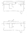
- Figure 1 is a cross section of a substrate 1 of semiconductor material carrying a device layer 2, which has an upper surface 10 and may be formed by a single layer or by a multiple layer.
- the device layer 2 can comprise any material used in semiconductor technology, like W, Al, Cu, Si, SiO 2 or Si 3 N 4 , for instance, which is to be structured in order to provide a special function of the semiconductor device.
- a recess 3 is formed extending from the surface 10 into the substrate 1.
- the recess 3 may especially be provided for a through substrate via, which provides an electric interconnect through the substrate 1.
- the device layer 2 is structured by means of a special mask technique.
- a dry film 4 which is provided as a mask layer 11, is applied on the surface 10 of the device layer 2, so that the dry film 4 covers the recess 3 and renders a planar upper surface of the device.
- An organic material may be especially suitable for the dry film 4, which is preferably applied with a thickness t in the range from 5 ⁇ m to 50 ⁇ m and can be formed by dry-film lamination or spin-on-coating, for example, with deliberately low step coverage. If the dry film 4 is formed from polyimide, it is stable in temperatures of up to 350°C.
- the resist layer 6 is preferably very thin, so that its thickness is much less than 1 ⁇ m, thus allowing for small structures to be resolved.
- a photolithography is performed, in which the resist layer 6 is subjected to a patterned light exposure and subsequent development, so that it can be partially removed according to the desired pattern by means of a solvent.
- Figure 2 is a cross section according to Figure 1 after the patterning of the resist layer 6 into a resist mask 16.
- Figure 3 is a cross section according to Figure 2 after structuring the dry film 4 into a dry film pattern 14 using the resist mask 16 as an etch mask.
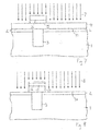
- the dry film etching 8 is indicated in Figure 3 by a plurality of arrows pointing downwards.
- the resist mask 16 is partially consumed during this etching step, which is indicated in Figure 3 by the layer representing the resist mask 16 being thinner than the corresponding layer in Figure 2 .
- the etching stops on the surface 10 of the device layer 2. As the dry film 4 had been applied sufficiently thick, the dry film pattern 14 still covers the recess 3.
- Figure 4 is a cross section according to Figure 3 after the structuring of the device layer 2. This is performed using the dry film pattern 14 as an etch mask.
- the device layer etching 9 is indicated in Figure 4 by a plurality of arrows pointing downwards. Residual portions of the device layer 2 remain under the dry film pattern 14 as the structured device layer 12.
- Figure 5 is a cross section according to Figure 1 for a further example of the method, in which a hardmask layer is applied as a further layer.
- Figure 5 shows a substrate 1 of semiconductor material carrying a device layer 2, which has an upper surface 10 and may be formed by a single layer or by a multiple layer.
- the device layer 2 can comprise any material used in semiconductor technology.
- a recess 3, which may especially be provided for a through substrate via, is formed extending from the surface 10 into the substrate 1.
- a dry film 4 is applied on the surface 10 of the device layer 2, and a hardmask layer 5 is applied on the dry film 4.
- the dry film 4 and the hardmask layer 5 are provided as a mask layer 11, which covers the recess 3 and renders a planar upper surface of the device.
- an organic material may be especially suitable for the dry film 4, which is preferably applied with a thickness t in the range from 5 ⁇ m to 50 ⁇ m. If the dry film 4 is formed from polyimide, it is stable in temperatures of up to 350°C.
- the hardmask layer 5 may be Si, SiO 2 , Si 3 N 4 , Al or another metal, for instance, and may be deposited at a temperature of typically less than 350°C to allow for thermal stability of the dry film 4. If a metal like Al is applied for the hardmask layer 5, sputtering or PVD (plasma-enhanced vapor deposition) at temperatures of less than 200°C is feasible and allows an application of a large variety of organic materials for the dry film 4.
- the resist layer 6 is preferably very thin, so that its thickness is much less than 1 ⁇ m, thus allowing for small structures to be resolved.
- a photolithography is performed, in which the resist layer 6 is subjected to a patterned light exposure and subsequent development, so that it can be partially removed according to the desired pattern by means of a solvent.
- Figure 6 is a cross section according to Figure 5 after the patterning of the resist layer 6 into a resist mask 16.
- Figure 7 is a cross section according to Figure 6 after structuring the hardmask layer 5 into a hardmask 15.
- the resist mask 16 is used as an etch mask.
- the hardmask layer etching 7 is indicated in Figure 7 by a plurality of arrows pointing downwards. If the etching process, which may be reactive ion etching (RIE), is selective with respect to the material of the dry film 4, the etching stops on the dry film 4.
- RIE reactive ion etching
- Figure 8 is a cross section according to Figure 7 after structuring the dry film 4 to form a dry film pattern 14.
- the hardmask 15 is used as an etch mask in this etching step, which may be reactive ion etching (RIE) using a chemistry based on CF 4 , for example.
- RIE reactive ion etching
- the residual portion of the resist mask 16 may be left on the hardmask 15 during the dry film etching, or it may be removed by O 2 , CF 4 /O 2 or another suitable chemistry before the etching of the dry film 4 takes place.
- the dry film etching 8 is indicated in Figure 8 by a plurality of arrows pointing downwards. The etching stops on the surface 10 of the device layer 2.
- the dry film pattern 14 and the hardmask 15 still cover the recess 3.
- the hardmask 15 may be left on the dry film pattern 14 or be removed, for example by using a suitable wet or dry etch process that is selective with respect to the dry film pattern 14.
- Figure 9 is a cross section according to Figure 8 after the structuring of the device layer 2. This is performed using the dry film pattern 14 as an etch mask. During the etching process the hardmask 15 may be left on the dry film pattern 14, as shown in Figure 9 as an example. Instead, the remaining portion of the resist mask 16 and the hardmask 15 may be removed before the device layer 2 is structured.
- the device layer etching 9 is indicated in Figure 9 by a plurality of arrows pointing downwards. Residual portions of the device layer 2 remain under the dry film pattern 14 as the structured device layer 12.
- Figure 10 is a cross section according to Figure 9 after the etching of the device layer 2.
- the broken lines in Figure 10 indicate an optional removal of the hardmask 15 and the dry film pattern 14, which can be removed using O 2 or CF 4 /O 2 or any other suitable chemistry, for example.
- the hardmask 15 and the dry film pattern 14 may instead be left as a cover of the recess 3 to close the inner volume 13.
- an additional hardmask layer 5 enables to pattern a dry film 4 that is much thicker than a dry film formed by a spin-on resist.
- a dry film that is insensitive to light can be used in the described method, a much better film strength can be achieved, which enhances the properties of the dry film that are important for an effective sealing of the recess 3.
- the mechanical stability of the cover of the recess is improved.
- very small feature sizes can be realized by the described method, which also obviates the need to apply special CMOS-incompatible developers.
Landscapes
- Drying Of Semiconductors (AREA)
- Internal Circuitry In Semiconductor Integrated Circuit Devices (AREA)
Priority Applications (1)
| Application Number | Priority Date | Filing Date | Title |
|---|---|---|---|
| EP13167088.7A EP2802004B1 (de) | 2013-05-08 | 2013-05-08 | Verfahren zur Strukturierung einer Vorrichtung aus einem vertieften Halbleitervorrichtung und vertieften Halbleitervorrichtung umfassend eine strukturierte Vorrichtungsschicht |
Applications Claiming Priority (1)
| Application Number | Priority Date | Filing Date | Title |
|---|---|---|---|
| EP13167088.7A EP2802004B1 (de) | 2013-05-08 | 2013-05-08 | Verfahren zur Strukturierung einer Vorrichtung aus einem vertieften Halbleitervorrichtung und vertieften Halbleitervorrichtung umfassend eine strukturierte Vorrichtungsschicht |
Publications (2)
| Publication Number | Publication Date |
|---|---|
| EP2802004A1 true EP2802004A1 (de) | 2014-11-12 |
| EP2802004B1 EP2802004B1 (de) | 2020-11-04 |
Family
ID=48227096
Family Applications (1)
| Application Number | Title | Priority Date | Filing Date |
|---|---|---|---|
| EP13167088.7A Active EP2802004B1 (de) | 2013-05-08 | 2013-05-08 | Verfahren zur Strukturierung einer Vorrichtung aus einem vertieften Halbleitervorrichtung und vertieften Halbleitervorrichtung umfassend eine strukturierte Vorrichtungsschicht |
Country Status (1)
| Country | Link |
|---|---|
| EP (1) | EP2802004B1 (de) |
Citations (8)
| Publication number | Priority date | Publication date | Assignee | Title |
|---|---|---|---|---|
| EP0665579A1 (de) | 1994-01-03 | 1995-08-02 | AT&T Corp. | Verfahren zur Herstellung eines Mehrschichtgitters mit geringerer Höhe |
| US20050048771A1 (en) | 2002-09-27 | 2005-03-03 | Advanced Micro Devices, Inc. | Hardmask employing multiple layers of silicon oxynitride |
| US20060009038A1 (en) * | 2004-07-12 | 2006-01-12 | International Business Machines Corporation | Processing for overcoming extreme topography |
| US20100038800A1 (en) * | 2008-08-18 | 2010-02-18 | Samsung Electronics Co., Ltd. | Through-silicon via structures including conductive protective layers and methods of forming the same |
| DE102009045385A1 (de) * | 2009-10-06 | 2011-04-07 | Robert Bosch Gmbh | Verfahren zum Verschließen eines Grabens eines mikromechanischen Bauelements |
| US20120068356A1 (en) * | 2010-09-21 | 2012-03-22 | Marcus Ahles | Component having a VIA |
| WO2012052039A1 (de) | 2010-10-19 | 2012-04-26 | Ev Group Gmbh | Vorrichtung zum beschichten eines wafers |
| US20120190204A1 (en) | 2011-01-26 | 2012-07-26 | International Business Machines Corporation | Non-conformal hardmask deposition for through silicon etch |
Family Cites Families (1)
| Publication number | Priority date | Publication date | Assignee | Title |
|---|---|---|---|---|
| US6696365B2 (en) * | 2002-01-07 | 2004-02-24 | Applied Materials, Inc. | Process for in-situ etching a hardmask stack |
-
2013
- 2013-05-08 EP EP13167088.7A patent/EP2802004B1/de active Active
Patent Citations (8)
| Publication number | Priority date | Publication date | Assignee | Title |
|---|---|---|---|---|
| EP0665579A1 (de) | 1994-01-03 | 1995-08-02 | AT&T Corp. | Verfahren zur Herstellung eines Mehrschichtgitters mit geringerer Höhe |
| US20050048771A1 (en) | 2002-09-27 | 2005-03-03 | Advanced Micro Devices, Inc. | Hardmask employing multiple layers of silicon oxynitride |
| US20060009038A1 (en) * | 2004-07-12 | 2006-01-12 | International Business Machines Corporation | Processing for overcoming extreme topography |
| US20100038800A1 (en) * | 2008-08-18 | 2010-02-18 | Samsung Electronics Co., Ltd. | Through-silicon via structures including conductive protective layers and methods of forming the same |
| DE102009045385A1 (de) * | 2009-10-06 | 2011-04-07 | Robert Bosch Gmbh | Verfahren zum Verschließen eines Grabens eines mikromechanischen Bauelements |
| US20120068356A1 (en) * | 2010-09-21 | 2012-03-22 | Marcus Ahles | Component having a VIA |
| WO2012052039A1 (de) | 2010-10-19 | 2012-04-26 | Ev Group Gmbh | Vorrichtung zum beschichten eines wafers |
| US20120190204A1 (en) | 2011-01-26 | 2012-07-26 | International Business Machines Corporation | Non-conformal hardmask deposition for through silicon etch |
Also Published As
| Publication number | Publication date |
|---|---|
| EP2802004B1 (de) | 2020-11-04 |
Similar Documents
| Publication | Publication Date | Title |
|---|---|---|
| US9373580B2 (en) | Dual hard mask lithography process | |
| US8314034B2 (en) | Feature size reduction | |
| US8586478B2 (en) | Method of making a semiconductor device | |
| US8894869B2 (en) | Lithography process using directed self assembly | |
| US8716151B2 (en) | Method of fabricating semiconductor devices | |
| US20090004862A1 (en) | Method for forming fine patterns in semiconductor device | |
| CN110416067B (zh) | 半导体装置的制造方法 | |
| TW201133548A (en) | Method for forming fine pattern | |
| CN108140730A (zh) | 以半加成电镀金属布线制造三维(3d)金属-绝缘体-金属(mim)电容器及电阻器的结构及方法 | |
| US8133664B2 (en) | Methods of forming patterns | |
| WO2010015301A8 (en) | Passivation of etched semiconductor structures | |
| US8828876B2 (en) | Dual mandrel sidewall image transfer processes | |
| KR100924611B1 (ko) | 반도체 소자의 미세 패턴 형성방법 | |
| US8329594B2 (en) | Method for fabricating a semiconductor structure | |
| US8372719B2 (en) | Hard mask removal for semiconductor devices | |
| TWI838397B (zh) | 用於形成包括具有不同介電厚度之兩個電容器的電子產品的方法和相對應的電子產品 | |
| US9691654B1 (en) | Methods and devices for back end of line via formation | |
| EP2802004B1 (de) | Verfahren zur Strukturierung einer Vorrichtung aus einem vertieften Halbleitervorrichtung und vertieften Halbleitervorrichtung umfassend eine strukturierte Vorrichtungsschicht | |
| US20080113515A1 (en) | Methods of Forming Semiconductor Devices | |
| US20190319089A1 (en) | Conformal capacitor structure formed by a single process | |
| US8476160B2 (en) | Sublithographic patterning employing image transfer of a controllably damaged dielectric sidewall | |
| US20150348787A1 (en) | Semiconductor devices and methods for forming a gate with reduced defects | |
| US20150140796A1 (en) | Formation of contact/via hole with self-alignment | |
| TWI715967B (zh) | 半導體結構及其製造方法 | |
| US20240128083A1 (en) | Semiconductor device structure with patterns having coplanar bottom surfaces and method for preparing the same |
Legal Events
| Date | Code | Title | Description |
|---|---|---|---|
| PUAI | Public reference made under article 153(3) epc to a published international application that has entered the european phase |
Free format text: ORIGINAL CODE: 0009012 |
|
| 17P | Request for examination filed |
Effective date: 20130508 |
|
| AK | Designated contracting states |
Kind code of ref document: A1 Designated state(s): AL AT BE BG CH CY CZ DE DK EE ES FI FR GB GR HR HU IE IS IT LI LT LU LV MC MK MT NL NO PL PT RO RS SE SI SK SM TR |
|
| AX | Request for extension of the european patent |
Extension state: BA ME |
|
| R17P | Request for examination filed (corrected) |
Effective date: 20150212 |
|
| RBV | Designated contracting states (corrected) |
Designated state(s): AL AT BE BG CH CY CZ DE DK EE ES FI FR GB GR HR HU IE IS IT LI LT LU LV MC MK MT NL NO PL PT RO RS SE SI SK SM TR |
|
| RAP1 | Party data changed (applicant data changed or rights of an application transferred) |
Owner name: AMS AG |
|
| STAA | Information on the status of an ep patent application or granted ep patent |
Free format text: STATUS: EXAMINATION IS IN PROGRESS |
|
| 17Q | First examination report despatched |
Effective date: 20190606 |
|
| GRAP | Despatch of communication of intention to grant a patent |
Free format text: ORIGINAL CODE: EPIDOSNIGR1 |
|
| STAA | Information on the status of an ep patent application or granted ep patent |
Free format text: STATUS: GRANT OF PATENT IS INTENDED |
|
| INTG | Intention to grant announced |
Effective date: 20200529 |
|
| GRAS | Grant fee paid |
Free format text: ORIGINAL CODE: EPIDOSNIGR3 |
|
| GRAA | (expected) grant |
Free format text: ORIGINAL CODE: 0009210 |
|
| STAA | Information on the status of an ep patent application or granted ep patent |
Free format text: STATUS: THE PATENT HAS BEEN GRANTED |
|
| AK | Designated contracting states |
Kind code of ref document: B1 Designated state(s): AL AT BE BG CH CY CZ DE DK EE ES FI FR GB GR HR HU IE IS IT LI LT LU LV MC MK MT NL NO PL PT RO RS SE SI SK SM TR |
|
| REG | Reference to a national code |
Ref country code: GB Ref legal event code: FG4D |
|
| REG | Reference to a national code |
Ref country code: CH Ref legal event code: EP |
|
| REG | Reference to a national code |
Ref country code: AT Ref legal event code: REF Ref document number: 1331906 Country of ref document: AT Kind code of ref document: T Effective date: 20201115 |
|
| REG | Reference to a national code |
Ref country code: DE Ref legal event code: R096 Ref document number: 602013073744 Country of ref document: DE |
|
| REG | Reference to a national code |
Ref country code: IE Ref legal event code: FG4D |
|
| REG | Reference to a national code |
Ref country code: NL Ref legal event code: MP Effective date: 20201104 |
|
| REG | Reference to a national code |
Ref country code: AT Ref legal event code: MK05 Ref document number: 1331906 Country of ref document: AT Kind code of ref document: T Effective date: 20201104 |
|
| PG25 | Lapsed in a contracting state [announced via postgrant information from national office to epo] |
Ref country code: GR Free format text: LAPSE BECAUSE OF FAILURE TO SUBMIT A TRANSLATION OF THE DESCRIPTION OR TO PAY THE FEE WITHIN THE PRESCRIBED TIME-LIMIT Effective date: 20210205 Ref country code: NO Free format text: LAPSE BECAUSE OF FAILURE TO SUBMIT A TRANSLATION OF THE DESCRIPTION OR TO PAY THE FEE WITHIN THE PRESCRIBED TIME-LIMIT Effective date: 20210204 Ref country code: PT Free format text: LAPSE BECAUSE OF FAILURE TO SUBMIT A TRANSLATION OF THE DESCRIPTION OR TO PAY THE FEE WITHIN THE PRESCRIBED TIME-LIMIT Effective date: 20210304 Ref country code: RS Free format text: LAPSE BECAUSE OF FAILURE TO SUBMIT A TRANSLATION OF THE DESCRIPTION OR TO PAY THE FEE WITHIN THE PRESCRIBED TIME-LIMIT Effective date: 20201104 Ref country code: FI Free format text: LAPSE BECAUSE OF FAILURE TO SUBMIT A TRANSLATION OF THE DESCRIPTION OR TO PAY THE FEE WITHIN THE PRESCRIBED TIME-LIMIT Effective date: 20201104 |
|
| PG25 | Lapsed in a contracting state [announced via postgrant information from national office to epo] |
Ref country code: LV Free format text: LAPSE BECAUSE OF FAILURE TO SUBMIT A TRANSLATION OF THE DESCRIPTION OR TO PAY THE FEE WITHIN THE PRESCRIBED TIME-LIMIT Effective date: 20201104 Ref country code: SE Free format text: LAPSE BECAUSE OF FAILURE TO SUBMIT A TRANSLATION OF THE DESCRIPTION OR TO PAY THE FEE WITHIN THE PRESCRIBED TIME-LIMIT Effective date: 20201104 Ref country code: PL Free format text: LAPSE BECAUSE OF FAILURE TO SUBMIT A TRANSLATION OF THE DESCRIPTION OR TO PAY THE FEE WITHIN THE PRESCRIBED TIME-LIMIT Effective date: 20201104 Ref country code: IS Free format text: LAPSE BECAUSE OF FAILURE TO SUBMIT A TRANSLATION OF THE DESCRIPTION OR TO PAY THE FEE WITHIN THE PRESCRIBED TIME-LIMIT Effective date: 20210304 Ref country code: BG Free format text: LAPSE BECAUSE OF FAILURE TO SUBMIT A TRANSLATION OF THE DESCRIPTION OR TO PAY THE FEE WITHIN THE PRESCRIBED TIME-LIMIT Effective date: 20210204 Ref country code: ES Free format text: LAPSE BECAUSE OF FAILURE TO SUBMIT A TRANSLATION OF THE DESCRIPTION OR TO PAY THE FEE WITHIN THE PRESCRIBED TIME-LIMIT Effective date: 20201104 Ref country code: AT Free format text: LAPSE BECAUSE OF FAILURE TO SUBMIT A TRANSLATION OF THE DESCRIPTION OR TO PAY THE FEE WITHIN THE PRESCRIBED TIME-LIMIT Effective date: 20201104 |
|
| REG | Reference to a national code |
Ref country code: LT Ref legal event code: MG9D |
|
| PG25 | Lapsed in a contracting state [announced via postgrant information from national office to epo] |
Ref country code: HR Free format text: LAPSE BECAUSE OF FAILURE TO SUBMIT A TRANSLATION OF THE DESCRIPTION OR TO PAY THE FEE WITHIN THE PRESCRIBED TIME-LIMIT Effective date: 20201104 |
|
| PG25 | Lapsed in a contracting state [announced via postgrant information from national office to epo] |
Ref country code: LT Free format text: LAPSE BECAUSE OF FAILURE TO SUBMIT A TRANSLATION OF THE DESCRIPTION OR TO PAY THE FEE WITHIN THE PRESCRIBED TIME-LIMIT Effective date: 20201104 Ref country code: SK Free format text: LAPSE BECAUSE OF FAILURE TO SUBMIT A TRANSLATION OF THE DESCRIPTION OR TO PAY THE FEE WITHIN THE PRESCRIBED TIME-LIMIT Effective date: 20201104 Ref country code: RO Free format text: LAPSE BECAUSE OF FAILURE TO SUBMIT A TRANSLATION OF THE DESCRIPTION OR TO PAY THE FEE WITHIN THE PRESCRIBED TIME-LIMIT Effective date: 20201104 Ref country code: EE Free format text: LAPSE BECAUSE OF FAILURE TO SUBMIT A TRANSLATION OF THE DESCRIPTION OR TO PAY THE FEE WITHIN THE PRESCRIBED TIME-LIMIT Effective date: 20201104 Ref country code: CZ Free format text: LAPSE BECAUSE OF FAILURE TO SUBMIT A TRANSLATION OF THE DESCRIPTION OR TO PAY THE FEE WITHIN THE PRESCRIBED TIME-LIMIT Effective date: 20201104 Ref country code: SM Free format text: LAPSE BECAUSE OF FAILURE TO SUBMIT A TRANSLATION OF THE DESCRIPTION OR TO PAY THE FEE WITHIN THE PRESCRIBED TIME-LIMIT Effective date: 20201104 |
|
| REG | Reference to a national code |
Ref country code: DE Ref legal event code: R097 Ref document number: 602013073744 Country of ref document: DE |
|
| PG25 | Lapsed in a contracting state [announced via postgrant information from national office to epo] |
Ref country code: DK Free format text: LAPSE BECAUSE OF FAILURE TO SUBMIT A TRANSLATION OF THE DESCRIPTION OR TO PAY THE FEE WITHIN THE PRESCRIBED TIME-LIMIT Effective date: 20201104 |
|
| PLBE | No opposition filed within time limit |
Free format text: ORIGINAL CODE: 0009261 |
|
| STAA | Information on the status of an ep patent application or granted ep patent |
Free format text: STATUS: NO OPPOSITION FILED WITHIN TIME LIMIT |
|
| 26N | No opposition filed |
Effective date: 20210805 |
|
| PG25 | Lapsed in a contracting state [announced via postgrant information from national office to epo] |
Ref country code: NL Free format text: LAPSE BECAUSE OF FAILURE TO SUBMIT A TRANSLATION OF THE DESCRIPTION OR TO PAY THE FEE WITHIN THE PRESCRIBED TIME-LIMIT Effective date: 20201104 Ref country code: AL Free format text: LAPSE BECAUSE OF FAILURE TO SUBMIT A TRANSLATION OF THE DESCRIPTION OR TO PAY THE FEE WITHIN THE PRESCRIBED TIME-LIMIT Effective date: 20201104 Ref country code: IT Free format text: LAPSE BECAUSE OF FAILURE TO SUBMIT A TRANSLATION OF THE DESCRIPTION OR TO PAY THE FEE WITHIN THE PRESCRIBED TIME-LIMIT Effective date: 20201104 |
|
| PG25 | Lapsed in a contracting state [announced via postgrant information from national office to epo] |
Ref country code: SI Free format text: LAPSE BECAUSE OF FAILURE TO SUBMIT A TRANSLATION OF THE DESCRIPTION OR TO PAY THE FEE WITHIN THE PRESCRIBED TIME-LIMIT Effective date: 20201104 |
|
| REG | Reference to a national code |
Ref country code: CH Ref legal event code: PL |
|
| GBPC | Gb: european patent ceased through non-payment of renewal fee |
Effective date: 20210508 |
|
| PG25 | Lapsed in a contracting state [announced via postgrant information from national office to epo] |
Ref country code: CH Free format text: LAPSE BECAUSE OF NON-PAYMENT OF DUE FEES Effective date: 20210531 Ref country code: MC Free format text: LAPSE BECAUSE OF FAILURE TO SUBMIT A TRANSLATION OF THE DESCRIPTION OR TO PAY THE FEE WITHIN THE PRESCRIBED TIME-LIMIT Effective date: 20201104 Ref country code: LI Free format text: LAPSE BECAUSE OF NON-PAYMENT OF DUE FEES Effective date: 20210531 Ref country code: LU Free format text: LAPSE BECAUSE OF NON-PAYMENT OF DUE FEES Effective date: 20210508 |
|
| REG | Reference to a national code |
Ref country code: BE Ref legal event code: MM Effective date: 20210531 |
|
| PG25 | Lapsed in a contracting state [announced via postgrant information from national office to epo] |
Ref country code: IE Free format text: LAPSE BECAUSE OF NON-PAYMENT OF DUE FEES Effective date: 20210508 Ref country code: GB Free format text: LAPSE BECAUSE OF NON-PAYMENT OF DUE FEES Effective date: 20210508 |
|
| PG25 | Lapsed in a contracting state [announced via postgrant information from national office to epo] |
Ref country code: IS Free format text: LAPSE BECAUSE OF FAILURE TO SUBMIT A TRANSLATION OF THE DESCRIPTION OR TO PAY THE FEE WITHIN THE PRESCRIBED TIME-LIMIT Effective date: 20210304 Ref country code: FR Free format text: LAPSE BECAUSE OF NON-PAYMENT OF DUE FEES Effective date: 20210531 |
|
| PG25 | Lapsed in a contracting state [announced via postgrant information from national office to epo] |
Ref country code: BE Free format text: LAPSE BECAUSE OF NON-PAYMENT OF DUE FEES Effective date: 20210531 |
|
| PG25 | Lapsed in a contracting state [announced via postgrant information from national office to epo] |
Ref country code: HU Free format text: LAPSE BECAUSE OF FAILURE TO SUBMIT A TRANSLATION OF THE DESCRIPTION OR TO PAY THE FEE WITHIN THE PRESCRIBED TIME-LIMIT; INVALID AB INITIO Effective date: 20130508 |
|
| PG25 | Lapsed in a contracting state [announced via postgrant information from national office to epo] |
Ref country code: CY Free format text: LAPSE BECAUSE OF FAILURE TO SUBMIT A TRANSLATION OF THE DESCRIPTION OR TO PAY THE FEE WITHIN THE PRESCRIBED TIME-LIMIT Effective date: 20201104 |
|
| P01 | Opt-out of the competence of the unified patent court (upc) registered |
Effective date: 20230822 |
|
| PG25 | Lapsed in a contracting state [announced via postgrant information from national office to epo] |
Ref country code: MK Free format text: LAPSE BECAUSE OF FAILURE TO SUBMIT A TRANSLATION OF THE DESCRIPTION OR TO PAY THE FEE WITHIN THE PRESCRIBED TIME-LIMIT Effective date: 20201104 |
|
| PG25 | Lapsed in a contracting state [announced via postgrant information from national office to epo] |
Ref country code: TR Free format text: LAPSE BECAUSE OF FAILURE TO SUBMIT A TRANSLATION OF THE DESCRIPTION OR TO PAY THE FEE WITHIN THE PRESCRIBED TIME-LIMIT Effective date: 20201104 |
|
| PG25 | Lapsed in a contracting state [announced via postgrant information from national office to epo] |
Ref country code: MT Free format text: LAPSE BECAUSE OF FAILURE TO SUBMIT A TRANSLATION OF THE DESCRIPTION OR TO PAY THE FEE WITHIN THE PRESCRIBED TIME-LIMIT Effective date: 20201104 |
|
| PGFP | Annual fee paid to national office [announced via postgrant information from national office to epo] |
Ref country code: DE Payment date: 20250521 Year of fee payment: 13 |