EP2801834A1 - Current sensor - Google Patents
Current sensor Download PDFInfo
- Publication number
- EP2801834A1 EP2801834A1 EP20120863825 EP12863825A EP2801834A1 EP 2801834 A1 EP2801834 A1 EP 2801834A1 EP 20120863825 EP20120863825 EP 20120863825 EP 12863825 A EP12863825 A EP 12863825A EP 2801834 A1 EP2801834 A1 EP 2801834A1
- Authority
- EP
- European Patent Office
- Prior art keywords
- mtj
- sensor
- bridge
- temperature compensation
- temperature
- Prior art date
- Legal status (The legal status is an assumption and is not a legal conclusion. Google has not performed a legal analysis and makes no representation as to the accuracy of the status listed.)
- Granted
Links
Images






Classifications
-
- G—PHYSICS
- G01—MEASURING; TESTING
- G01R—MEASURING ELECTRIC VARIABLES; MEASURING MAGNETIC VARIABLES
- G01R19/00—Arrangements for measuring currents or voltages or for indicating presence or sign thereof
- G01R19/0092—Measuring current only
-
- G—PHYSICS
- G01—MEASURING; TESTING
- G01R—MEASURING ELECTRIC VARIABLES; MEASURING MAGNETIC VARIABLES
- G01R19/00—Arrangements for measuring currents or voltages or for indicating presence or sign thereof
- G01R19/32—Compensating for temperature change
-
- G—PHYSICS
- G01—MEASURING; TESTING
- G01R—MEASURING ELECTRIC VARIABLES; MEASURING MAGNETIC VARIABLES
- G01R15/00—Details of measuring arrangements of the types provided for in groups G01R17/00 - G01R29/00, G01R33/00 - G01R33/26 or G01R35/00
- G01R15/14—Adaptations providing voltage or current isolation, e.g. for high-voltage or high-current networks
- G01R15/20—Adaptations providing voltage or current isolation, e.g. for high-voltage or high-current networks using galvano-magnetic devices, e.g. Hall-effect devices, i.e. measuring a magnetic field via the interaction between a current and a magnetic field, e.g. magneto resistive or Hall effect devices
- G01R15/205—Adaptations providing voltage or current isolation, e.g. for high-voltage or high-current networks using galvano-magnetic devices, e.g. Hall-effect devices, i.e. measuring a magnetic field via the interaction between a current and a magnetic field, e.g. magneto resistive or Hall effect devices using magneto-resistance devices, e.g. field plates
-
- G—PHYSICS
- G01—MEASURING; TESTING
- G01R—MEASURING ELECTRIC VARIABLES; MEASURING MAGNETIC VARIABLES
- G01R17/00—Measuring arrangements involving comparison with a reference value, e.g. bridge
- G01R17/10—AC or DC measuring bridges
-
- G—PHYSICS
- G01—MEASURING; TESTING
- G01R—MEASURING ELECTRIC VARIABLES; MEASURING MAGNETIC VARIABLES
- G01R33/00—Arrangements or instruments for measuring magnetic variables
- G01R33/02—Measuring direction or magnitude of magnetic fields or magnetic flux
- G01R33/06—Measuring direction or magnitude of magnetic fields or magnetic flux using galvano-magnetic devices
-
- G—PHYSICS
- G01—MEASURING; TESTING
- G01R—MEASURING ELECTRIC VARIABLES; MEASURING MAGNETIC VARIABLES
- G01R33/00—Arrangements or instruments for measuring magnetic variables
- G01R33/02—Measuring direction or magnitude of magnetic fields or magnetic flux
- G01R33/06—Measuring direction or magnitude of magnetic fields or magnetic flux using galvano-magnetic devices
- G01R33/09—Magnetoresistive devices
- G01R33/098—Magnetoresistive devices comprising tunnel junctions, e.g. tunnel magnetoresistance sensors
Definitions
- the present invention relates to a current sensor, in particular a magnetic tunnel junction current sensor utilizing a magnetic tunnel junction resistor for temperature compensation.
- the Hall Effect is commonly used in the sensing element of current sensors. Additionally but less commonly, the anisotropic magnetoresistance (AMR) and the giant magnetoresistance (GMR) effects are also used in the sensing elements of current sensors. What these effects have in common is they can be used to build a magnetic sensor in order to measure the magnetic field generated by a current flowing through a conductor, which is proportional to the value of the current flowing through the conductor.
- AMR anisotropic magnetoresistance
- GMR giant magnetoresistance
- Hall sensors Because the sensitivity of Hall elements is very low, when Hall elements are used in current sensors, a magnetic flux concentrator is usually used to amplify the magnetic field, in order to increase the sensitivity of the Hall sensor. Unfortunately this increases the size and weight of the current sensor, and it degrades linearity. Additionally, Hall sensors have high power consumption, which is undesirable. Although AMR sensors have much higher sensitivity than Hall sensors, AMR sensors have narrower linear range, and they require a set / reset coil, resulting in manufacturing process complexity, increased size, and increased power consumption. GMR sensors also have higher sensitivity than Hall sensors, but the linear range is also narrow.
- Magnetic tunnel junctions are beginning to find application as magnetoresistive sensors for industrial applications. They use the tunneling magnetoresistance (TMR) effect of a multilayered magnetic material stack to sense the magnitude and direction of a magnetic field, with significantly larger sensitivity than AMR, Hall, and GMR sensors, while also providing better temperature stability.
- TMR tunneling magnetoresistance
- a current sensor utilizing MTJ sensing elements provides improved temperature stability, higher sensitivity, lower power consumption, and better linearity than a Hall effect based current sensor with no additional magnetic flux concentrator structure; compared to AMR current sensors it provides improved temperature stability, higher sensitivity, wider linear range without additional set / reset coil structure; and, compared to GMR based current sensors, it provides better temperature stability, higher sensitivity, lower power consumption, and wider linear range.
- the present invention provides a current sensor using MTJ elements both to sense the magnetic field from the current and to compensate temperature drift thereby providing high sensitivity, wide linear range, low power consumption, small size, and good temperature performance characteristics.
- the present invention provides a single chip current sensor comprising a MTJ sensor bridge containing one or more MTJ elements, an electric conductor in the vicinity of the sensor bridge that carries a test electric current, and at least one MTJ temperature compensation resistors, wherein magnets are placed on the sides of the one or more MTJ temperature compensation resistors producing a magnetic field to bias the free layer of the MTJ elements in the temperature compensation resistors such that the direction of the magnetization of the free layer of each of the MTJ temperature compensation elements is anti parallel to the direction of the magnetization of its pinned layer, such that the one or more MTJ temperature compensation resistors are in a high resistance state that only changes as the function of temperature in the measurement range of the current sensor, wherein the sensor bridge is connected in series with the one or more MTJ temperature compensation resistors so as to stabilize the sensor bridge voltage output, and the sensor bridge determines the test electric current by measuring the magnetic field produced by the test electric current in the electric conductor which is provided as an output voltage.
- the MTJ sensor bridge and the one or more MTJ temperature compensation resistors respectively comprise one or more MTJ elements connected in series, wherein said MTJ elements have the same temperature coefficient, R H , and R L .
- the sensor bridge is a half bridge.
- the sensor bridge is a full bridge.
- the present invention uses the above structure to compensate for temperature drift of the current sensor while providing the benefits of high sensitivity, wide linear range, low power consumption, small size, and excellent thermal stability.
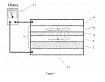
- FIG. 1 schematically illustrates the multilayer film and operational concept of an MTJ element.
- An MTJ element 1 generally includes a synthetic antiferromagnet (SAF) 3, and another ferromagnetic layer or 5, between on opposing sides of a tunnel barrier layer 4.
- the upper layer is the free layer whose magnetization direction is changed in response to the external magnetic field.
- the lower ferromagnetic layer (SAF layer) 3 is a fixed magnetic layer, and its magnetization direction is rigidly pinned in one direction, so that under normal conditions, it will not change.
- the pinning layer 2 is usually an antiferromagnetic material that can be deposited above or below a pinned layer SAF.
- the MTJ structure is usually deposited on top of a conductive seed layer 10 for use as the bottom electrode, while another conductive capping layer 6 is deposited on top of the MTJ structure.
- the resistance 11 of the MTJ element is measured between the seed layer 10 and the capping layer 6, and it represents the relative orientation of the free layer 5 and the pinned layer 3 magnetization directions.
- the resistance 11 of the MTJ element will be representative of the low resistance state.
- the overall resistance of the element 11 will be representative of the high resistance state.
- MTJ element 1 can be fabricated such that the change in resistance between the low and high resistance states is linearly dependent on magnetic field.
- Figure 2 shows the linear response of a MTJ magnetoresistive element 1.
- the output curve When saturated, the output curve will be in either the low resistance 12 or high resistance 13 states.
- the MTJ element 1 When the magnetization direction of the pinned layer 8 is parallel to the magnetization direction of the free layer 7, the MTJ element 1 is a low-resistance state 12; when the magnetization direction of the pinned layer 8 is anti-parallel to the magnetization direction of the free layer 7, the MTJ element 1 is a high-resistance state 13.
- the output curve Before saturation is reached, the output curve is linearly dependent on the applied magnetic field H.
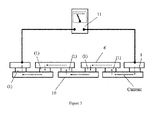
- Figure 3 shows several MTJ elements 1 is connected in series to form a MTJ magnetoresistor.
- This series connected MTJ magnetoresistance structure helps to reduce noise and improve stability of the sensor.
- the bias voltage of each of the MTJ element 1 decreases as the number of magnetic tunnel junctions increases. This reduces the current required to produce a large output voltage, thus reducing shot noise, along with the increasing ESD immunity.
- the noise of the MTJ is correspondingly reduced, because the uncorrelated random variation of each MTJ element 1 averages out.
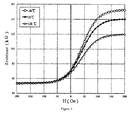
- Figure 4 shows MTJ output curves acquired at various different temperatures, it shows that as the temperature rises, the MTJ element low resistance does not change significantly, but the high resistance value changes significantly, such that overall, MTJ magnetoresistance decreases with increasing temperature.
- FIG 5 is a schematic diagram of a push-pull half-bridge MTJ sensor.
- the two MTJ resistors R1, R2 have anti-parallel pinned layer magnetization directions, and the magnetization direction of the free layer 7 changes in response to the external magnetic field, a steady voltage, Vbias, is applied between the Vcc and GND terminal pads, and the Vout pad is the bridge output.
- Vbias a steady voltage
- the magnetic field component along the sensitive direction 9 increases the resistance of resistor R1 while decreasing the resistance of resistor R2, when applied in the opposite direction the magnetic field decreases the resistance of resistor R1 while increasing the resistance of resistor R2.
- the typical push-pull half-bridge sensor output curve is shown in Figure 6 .
- Figure 7 shows the simulated output of a push-pull half-bridge MTJ sensor at different temperatures. As shown, the output voltage of the half-bridge circuit is reduced as the temperature rises.
- Figure 8 schematically illustrates a push-pull full-bridge MTJ sensor.
- the figure four MTJ resistors R11, R12, R21, R22 are connected in a full bridge configuration, a steady bias voltage is applied between the Vbias and GND terminal pads, the pads V + and V-are the output terminals, the magnetization direction of the free layer 7 of the four resistors changes in response to an externally applied magnetic field, resistors R11 and R22 (R12 and R21) have a pinned layer magnetization 8 pointing in the same direction, the adjacent resistors R11 and R12 (R11 and R21, etc.) have their pinned layer magnetizations 8 pointing in opposite directions, the sensitive direction 9 of the bridge circuit is along the axis parallel and antiparallel to the pinned layer direction 8.
- V H V ⁇ 1 H - V ⁇ 2 H
- V H R H - R L R H + R L ⁇ H H s ⁇ V bias
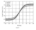
- Figure 10 shows a simulation of the MTJ push-pull full-bridge circuit output at different temperatures. It clearly indicates that as the temperature increases, the output voltage of the bridge circuit is reduced.
- FIG 11 schematically illustrates a temperature compensation resistor 16 on a chip connected with a MTJ half-bridge circuit. As shown, the half-bridge circuit 14 is connected in series with the temperature compensation resistor 16. Temperature compensation resistor 16 is biased by the magnetic field of permanent magnet 17 setting the magnetization direction of the free layer 7, so that it is antiparallel to the magnetization direction of the pinned layer 8 and therefore in the high resistance state 13, and the external field does not change the resistance 11 within the measurement temperature range.
- the chip is provided with a conductor 20 in which the measured current 19 flows between the I in+ and I in- pads, the sensor bridge circuit 14 detects the magnetic field 21 produced by the current 19.
- temperature compensation resistor 16 has the same temperature coefficient as half-bridge arm resistors R1, R2 such that the effect of temperature cancels out, when the magnetoresistance changes with temperature, the temperature compensation resistor and the bridge circuit move higher and lower respectively at the same time, such that the output of the bridge is stable against temperature, providing the temperature compensation.
- Figure 12 shows another single-chip MTJ half-bridge plus temperature compensation resistor 16 arrangement.
- the bridge resistors R1 and R2 have pinned layer magnetization 8 pointing in the same direction, while the magnetization direction of the free layer 7 varies in response to the external field, half bridge circuit 14 and the temperature compensation resistor 16 are connected in series, temperature compensation resistor 16 is biased with a strong permanent magnet 17 to set the magnetization direction of the free layer 7, antiparallel to the magnetization direction of the pinned layer 8 such that the resistance is in the high resistance state 13, and the external field does not change the resistance 11 within the measurement temperature range.
- the chip is provided with a U-shaped conductor 20 above or below resistors R1 and R2 in which the measured current 19 flows between the I in+ and I in- pads, the sensor bridge circuit 14 detects the magnetic field 21 produced by the current 19.
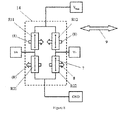
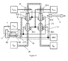
- Figure 13 shows another single-chip MTJ full-bridge plus temperature compensation resistor 16 arrangement.
- the four MTJ resistors R11, R12, R21, and R22 are interconnected as full-bridge and connected in series with temperature compensation resistor 16, the four MTJ resistors have magnetization direction 8 of the pinned layer rigidly aligned in the same direction and the free layers 7 change in response to the external magnetic field, , temperature compensation resistor 16 is biased with a strong permanent magnet 17 to set the magnetization direction of the free layer 7, antiparallel to the magnetization direction of the pinned layer 8 such that the resistance is in the high resistance state 13, and the external field does not change the resistance 11 within the measurement temperature range.
- the chip is provided with a U-shaped conductor 20 in which the measured current 19 flows between the I in+ and I in- pads, the sensor bridge circuit 14 detects the magnetic field 21 produced by the current 19.
- V OUT T V OUT ⁇ 1 + k T ⁇ ⁇ ⁇ T
- the "kT” is the temperature coefficient of the bridge, where in Hall current sensors kT is commonly expressed in terms of PPM/C.
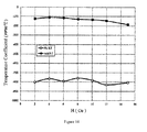
- Figure 14 shows testing results for the temperature coefficient of a MTJ push-pull full-bridge with and without a temperature compensating resistor, we can clearly see, before removing the temperature compensating resistor, the temperature coefficient is much smaller, therefore the effect of the temperature compensating resistor is obvious.
Landscapes
- Physics & Mathematics (AREA)
- General Physics & Mathematics (AREA)
- Condensed Matter Physics & Semiconductors (AREA)
- Measuring Magnetic Variables (AREA)
- Hall/Mr Elements (AREA)
- Measuring Instrument Details And Bridges, And Automatic Balancing Devices (AREA)
Abstract
Description
- The present invention relates to a current sensor, in particular a magnetic tunnel junction current sensor utilizing a magnetic tunnel junction resistor for temperature compensation.
- The Hall Effect is commonly used in the sensing element of current sensors. Additionally but less commonly, the anisotropic magnetoresistance (AMR) and the giant magnetoresistance (GMR) effects are also used in the sensing elements of current sensors. What these effects have in common is they can be used to build a magnetic sensor in order to measure the magnetic field generated by a current flowing through a conductor, which is proportional to the value of the current flowing through the conductor.
- Because the sensitivity of Hall elements is very low, when Hall elements are used in current sensors, a magnetic flux concentrator is usually used to amplify the magnetic field, in order to increase the sensitivity of the Hall sensor. Unfortunately this increases the size and weight of the current sensor, and it degrades linearity. Additionally, Hall sensors have high power consumption, which is undesirable. Although AMR sensors have much higher sensitivity than Hall sensors, AMR sensors have narrower linear range, and they require a set / reset coil, resulting in manufacturing process complexity, increased size, and increased power consumption. GMR sensors also have higher sensitivity than Hall sensors, but the linear range is also narrow.
- Magnetic tunnel junctions (MTJ) are beginning to find application as magnetoresistive sensors for industrial applications. They use the tunneling magnetoresistance (TMR) effect of a multilayered magnetic material stack to sense the magnitude and direction of a magnetic field, with significantly larger sensitivity than AMR, Hall, and GMR sensors, while also providing better temperature stability. Thus a current sensor utilizing MTJ sensing elements provides improved temperature stability, higher sensitivity, lower power consumption, and better linearity than a Hall effect based current sensor with no additional magnetic flux concentrator structure; compared to AMR current sensors it provides improved temperature stability, higher sensitivity, wider linear range without additional set / reset coil structure; and, compared to GMR based current sensors, it provides better temperature stability, higher sensitivity, lower power consumption, and wider linear range.
- Although temperature characteristics of a TMR based current sensor are superior to Hall Effect, AMR, and GMR based current sensors, temperature compensation is still necessary for high accuracy.
- The present invention provides a current sensor using MTJ elements both to sense the magnetic field from the current and to compensate temperature drift thereby providing high sensitivity, wide linear range, low power consumption, small size, and good temperature performance characteristics.
- To achieve the above object, the present invention provides a single chip current sensor comprising a MTJ sensor bridge containing one or more MTJ elements, an electric conductor in the vicinity of the sensor bridge that carries a test electric current, and at least one MTJ temperature compensation resistors, wherein magnets are placed on the sides of the one or more MTJ temperature compensation resistors producing a magnetic field to bias the free layer of the MTJ elements in the temperature compensation resistors such that the direction of the magnetization of the free layer of each of the MTJ temperature compensation elements is anti parallel to the direction of the magnetization of its pinned layer, such that the one or more MTJ temperature compensation resistors are in a high resistance state that only changes as the function of temperature in the measurement range of the current sensor, wherein the sensor bridge is connected in series with the one or more MTJ temperature compensation resistors so as to stabilize the sensor bridge voltage output, and the sensor bridge determines the test electric current by measuring the magnetic field produced by the test electric current in the electric conductor which is provided as an output voltage.
- Preferably, the MTJ sensor bridge and the one or more MTJ temperature compensation resistors respectively comprise one or more MTJ elements connected in series, wherein said MTJ elements have the same temperature coefficient, RH, and RL.
- Preferably, the sensor bridge is a half bridge.
- Preferably, the sensor bridge is a full bridge.
- The present invention uses the above structure to compensate for temperature drift of the current sensor while providing the benefits of high sensitivity, wide linear range, low power consumption, small size, and excellent thermal stability.
-
-
Figure 1 is a diagram of a magnetic tunnel junction element. -
Figure 2 shows a plot of the transfer curve of a MTJ linear magnetic field sensing element with magnetic field applied along the hard axis direction. -
Figure 3 shows how several MTJ elements can be connected in series to form a magnetoresistor. -
Figure 4 shows the magnetoresistive transfer curve of an MTJ element at different temperatures. -
Figure 5 is a schematic diagram of a push-pull half-bridge MTJ sensor. -
Figure 6 shows the typical output of a push-pull half-bridge MTJ sensor. -
Figure 7 shows the simulated output of a push-pull half-bridge MTJ sensor at different temperatures. -
Figure 8 is a schematic diagram of a push-pull full-bridge MTJ sensor. -
Figure 9 shows the typical output of a push-pull full-bridge MTJ sensor. -
Figure 10 shows the simulated output of a push-pull full-bridge MTJ sensor at different temperatures. -
Figure 11 illustrates the concept of temperature compensation resistors applied to a half-bridge TMR current sensor. -
Figure 12 shows another arrangement for implementing a temperature compensation resistor within a half-bridge MTJ current sensor. -
Figure 13 illustrates a concept for using a temperature compensation resistor within a full-bridge MTJ current sensor. -
Figure 14 shows a plot of two different curves for the temperature dependence of the output of temperature compensated and uncompensated MTJ current sensors. -
Figure 1 schematically illustrates the multilayer film and operational concept of an MTJ element. AnMTJ element 1 generally includes a synthetic antiferromagnet (SAF) 3, and another ferromagnetic layer or 5, between on opposing sides of atunnel barrier layer 4. In this structure, the upper layer is the free layer whose magnetization direction is changed in response to the external magnetic field. The lower ferromagnetic layer (SAF layer) 3 is a fixed magnetic layer, and its magnetization direction is rigidly pinned in one direction, so that under normal conditions, it will not change. Thepinning layer 2 is usually an antiferromagnetic material that can be deposited above or below a pinned layer SAF. The MTJ structure is usually deposited on top of aconductive seed layer 10 for use as the bottom electrode, while anotherconductive capping layer 6 is deposited on top of the MTJ structure. Theresistance 11 of the MTJ element is measured between theseed layer 10 and thecapping layer 6, and it represents the relative orientation of thefree layer 5 and the pinned layer 3 magnetization directions. When the upper ferromagneticfree layer 5 and the lower the lower ferromagnetic pinning layer magnetization directions are parallel to each other, theresistance 11 of the MTJ element will be representative of the low resistance state. When the upper ferromagneticfree layer 5 lower ferromagnetic pinned layer 3 magnetization directions are antiparallel to each other, the overall resistance of theelement 11 will be representative of the high resistance state. By known techniques,MTJ element 1, can be fabricated such that the change in resistance between the low and high resistance states is linearly dependent on magnetic field. -
Figure 2 shows the linear response of a MTJmagnetoresistive element 1. When saturated, the output curve will be in either thelow resistance 12 orhigh resistance 13 states. When the magnetization direction of thepinned layer 8 is parallel to the magnetization direction of thefree layer 7, theMTJ element 1 is a low-resistance state 12; when the magnetization direction of thepinned layer 8 is anti-parallel to the magnetization direction of thefree layer 7, theMTJ element 1 is a high-resistance state 13. Before saturation is reached, the output curve is linearly dependent on the applied magnetic field H. The output curve is usually not symmetric about H = 0. Typically thesaturation fields resistance state 12 saturation point is closer to H = 0. The offset value is often referred to as "orange peel coupling" or "Neel coupling," the typical value of this offset is usually between 1 and 25 Oe, and the roughness of theMTJ element 1, the influence the effect, making it dependent on materials and manufacturing processes. Between the saturated regions, the output curve equation can be approximated as:
-
Figure 3 showsseveral MTJ elements 1 is connected in series to form a MTJ magnetoresistor. This series connected MTJ magnetoresistance structure helps to reduce noise and improve stability of the sensor. In the MTJ magnetoresistor, the bias voltage of each of theMTJ element 1, decreases as the number of magnetic tunnel junctions increases. This reduces the current required to produce a large output voltage, thus reducing shot noise, along with the increasing ESD immunity. In addition, as the number ofMTJ elements 1 is increased, the noise of the MTJ is correspondingly reduced, because the uncorrelated random variation of eachMTJ element 1 averages out. -
Figure 4 shows MTJ output curves acquired at various different temperatures, it shows that as the temperature rises, the MTJ element low resistance does not change significantly, but the high resistance value changes significantly, such that overall, MTJ magnetoresistance decreases with increasing temperature. -
Figure 5 is a schematic diagram of a push-pull half-bridge MTJ sensor. As shown, the two MTJ resistors R1, R2 have anti-parallel pinned layer magnetization directions, and the magnetization direction of thefree layer 7 changes in response to the external magnetic field, a steady voltage, Vbias, is applied between the Vcc and GND terminal pads, and the Vout pad is the bridge output. When applying an external magnetic field to the push-pull half-bridge sensor, the magnetic field component along thesensitive direction 9 increases the resistance of resistor R1 while decreasing the resistance of resistor R2, when applied in the opposite direction the magnetic field decreases the resistance of resistor R1 while increasing the resistance of resistor R2. The typical push-pull half-bridge sensor output curve is shown inFigure 6 . -
Figure 7 shows the simulated output of a push-pull half-bridge MTJ sensor at different temperatures. As shown, the output voltage of the half-bridge circuit is reduced as the temperature rises. -
Figure 8 schematically illustrates a push-pull full-bridge MTJ sensor. As shown n the figure four MTJ resistors R11, R12, R21, R22 are connected in a full bridge configuration, a steady bias voltage is applied between the Vbias and GND terminal pads, the pads V + and V-are the output terminals, the magnetization direction of thefree layer 7 of the four resistors changes in response to an externally applied magnetic field, resistors R11 and R22 (R12 and R21) have a pinnedlayer magnetization 8 pointing in the same direction, the adjacent resistors R11 and R12 (R11 and R21, etc.) have their pinnedlayer magnetizations 8 pointing in opposite directions, thesensitive direction 9 of the bridge circuit is along the axis parallel and antiparallel to the pinnedlayer direction 8. - When applying a magnetic field to the full-bridge push-pull, the component of the magnetic field along the
sensitive direction 9 increases the resistance of resistors R11 and R22 while decreasing the resistance of the other two resistors R12 and R21, when the polarity of the applied magnetic field is changed the resistance of R11 and R22 is decreased while the resistance of R12 and R21 increases accordingly, using two pairs of resistors with the opposite response-one pair of resistors has increasing response while another has decreasing response - can increase the sensitivity of the bridge circuit output. This arrangement is called a "push-pull" full-bridge circuit. The output voltage of each half is defined:

- The combined bridge output is defined as:

- In the bridge circuit, the MTJ resistance values may be defined as:


- Such that:

- This is the output of the push-pull full-bridge, and a simulated output curve is shown in
Figure 9 . -
Figure 10 shows a simulation of the MTJ push-pull full-bridge circuit output at different temperatures. It clearly indicates that as the temperature increases, the output voltage of the bridge circuit is reduced. - It is not difficult to see, the MTJ bridge output drifts with temperature because the MTJ elements resistance changes leading to a change in output voltage. To compensate the temperature drift, a temperature compensating resistor can be used.
FIG 11 schematically illustrates atemperature compensation resistor 16 on a chip connected with a MTJ half-bridge circuit. As shown, the half-bridge circuit 14 is connected in series with thetemperature compensation resistor 16.Temperature compensation resistor 16 is biased by the magnetic field ofpermanent magnet 17 setting the magnetization direction of thefree layer 7, so that it is antiparallel to the magnetization direction of the pinnedlayer 8 and therefore in thehigh resistance state 13, and the external field does not change theresistance 11 within the measurement temperature range. The chip is provided with aconductor 20 in which the measured current 19 flows between the Iin+ and Iin- pads, thesensor bridge circuit 14 detects themagnetic field 21 produced by the current 19. Ideallytemperature compensation resistor 16 has the same temperature coefficient as half-bridge arm resistors R1, R2 such that the effect of temperature cancels out, when the magnetoresistance changes with temperature, the temperature compensation resistor and the bridge circuit move higher and lower respectively at the same time, such that the output of the bridge is stable against temperature, providing the temperature compensation. -
Figure 12 shows another single-chip MTJ half-bridge plustemperature compensation resistor 16 arrangement. As shown in the figure, the bridge resistors R1 and R2, have pinnedlayer magnetization 8 pointing in the same direction, while the magnetization direction of thefree layer 7 varies in response to the external field,half bridge circuit 14 and thetemperature compensation resistor 16 are connected in series,temperature compensation resistor 16 is biased with a strongpermanent magnet 17 to set the magnetization direction of thefree layer 7, antiparallel to the magnetization direction of the pinnedlayer 8 such that the resistance is in thehigh resistance state 13, and the external field does not change theresistance 11 within the measurement temperature range. The chip is provided with aU-shaped conductor 20 above or below resistors R1 and R2 in which the measured current 19 flows between the Iin+ and Iin- pads, thesensor bridge circuit 14 detects themagnetic field 21 produced by the current 19. -
Figure 13 shows another single-chip MTJ full-bridge plustemperature compensation resistor 16 arrangement. As shown, the four MTJ resistors R11, R12, R21, and R22 are interconnected as full-bridge and connected in series withtemperature compensation resistor 16, the four MTJ resistors have magnetizationdirection 8 of the pinned layer rigidly aligned in the same direction and thefree layers 7 change in response to the external magnetic field, ,temperature compensation resistor 16 is biased with a strongpermanent magnet 17 to set the magnetization direction of thefree layer 7, antiparallel to the magnetization direction of the pinnedlayer 8 such that the resistance is in thehigh resistance state 13, and the external field does not change theresistance 11 within the measurement temperature range. The chip is provided with aU-shaped conductor 20 in which the measured current 19 flows between the Iin+ and Iin- pads, thesensor bridge circuit 14 detects themagnetic field 21 produced by the current 19. - The output of the bridge circuit Vout(T) and the actual output voltage Vout of the bridge are linearly related by the following function:

- The "kT" is the temperature coefficient of the bridge, where in Hall current sensors kT is commonly expressed in terms of PPM/C.
Figure 14 shows testing results for the temperature coefficient of a MTJ push-pull full-bridge with and without a temperature compensating resistor, we can clearly see, before removing the temperature compensating resistor, the temperature coefficient is much smaller, therefore the effect of the temperature compensating resistor is obvious. - While specific implementations of the present invention are illustrated, obviously, various modifications of the invention may be made without departing from the spirit or scope of the invention. Those skilled in the art of the present invention understand that the spirit and intent of the present invention is not changed by such modifications.
Claims (4)
- A single chip current sensor comprising a MTJ sensor bridge containing one or more MTJ resistors, an electric conductor in the vicinity of the sensor bridge that carries a test electric current, and at least one MTJ temperature compensation resistor, wherein magnets are placed on the sides of the one or more MTJ temperature compensation resistors producing a magnetic field to bias the free layer of the MTJ elements in the one or more temperature compensation resistors such that the direction of the magnetization of the free layer of each of the MTJ elements in the temperature compensation resistors is anti-parallel to the direction of the magnetization of its pinned layer, such that the one or more MTJ temperature compensation resistors are in a high resistance state that only changes as the function of temperature in the measurement range of the current sensor, wherein the sensor bridge is connected in series with the one or more MTJ temperature compensation resistors so as to stabilize the sensor bridge voltage output, and the sensor bridge determines the test electric current by measuring the magnetic field produced by the test electric current in the electric conductor which is then provided as an output voltage.
- The single chip current sensor of claim 1, wherein the MTJ resistors and the one or more MTJ temperature compensation resistors respectively comprise one or more MTJ elements connected in series, wherein said MTJ elements have the same temperature coefficient, RH, and RL.
- The single chip current sensor of claim 1, wherein the sensor bridge is a half bridge.
- The single chip current sensor of claim 1, wherein the sensor bridge is a full bridge.
Applications Claiming Priority (2)
| Application Number | Priority Date | Filing Date | Title |
|---|---|---|---|
| CN2011104528342A CN102419393B (en) | 2011-12-30 | 2011-12-30 | Current sensor |
| PCT/CN2012/083742 WO2013097542A1 (en) | 2011-12-30 | 2012-10-30 | Current sensor |
Publications (3)
| Publication Number | Publication Date |
|---|---|
| EP2801834A1 true EP2801834A1 (en) | 2014-11-12 |
| EP2801834A4 EP2801834A4 (en) | 2015-12-09 |
| EP2801834B1 EP2801834B1 (en) | 2024-06-12 |
Family
ID=45943900
Family Applications (1)
| Application Number | Title | Priority Date | Filing Date |
|---|---|---|---|
| EP12863825.1A Active EP2801834B1 (en) | 2011-12-30 | 2012-10-30 | Current sensor |
Country Status (5)
| Country | Link |
|---|---|
| US (1) | US9465056B2 (en) |
| EP (1) | EP2801834B1 (en) |
| JP (1) | JP6403326B2 (en) |
| CN (1) | CN102419393B (en) |
| WO (1) | WO2013097542A1 (en) |
Cited By (1)
| Publication number | Priority date | Publication date | Assignee | Title |
|---|---|---|---|---|
| EP3029479A4 (en) * | 2013-07-30 | 2017-03-15 | Multidimension Technology Co., Ltd. | Singlechip push-pull bridge type magnetic field sensor |
Families Citing this family (56)
| Publication number | Priority date | Publication date | Assignee | Title |
|---|---|---|---|---|
| CN102419393B (en) | 2011-12-30 | 2013-09-04 | 江苏多维科技有限公司 | Current sensor |
| CN102565727B (en) * | 2012-02-20 | 2016-01-20 | 江苏多维科技有限公司 | For measuring the magnetic resistance sensor in magnetic field |
| CN103217570B (en) * | 2013-03-21 | 2015-04-15 | 无锡凌湖科技有限公司 | Tunneling magneto resistive (TMR) self-temperature-compensation digital current sensor |
| CN103226165B (en) * | 2013-04-08 | 2015-04-08 | 无锡凌湖科技有限公司 | TMR self-zeroing digital current sensor and self-zeroing method thereof |
| CN103384141B (en) * | 2013-07-24 | 2015-05-06 | 江苏多维科技有限公司 | Magnetic-resistance mixer |
| JP6105817B2 (en) * | 2013-11-01 | 2017-03-29 | 中国科学院物理研究所 | Nanomagnetic multilayer film for temperature sensor and its manufacturing method |
| CN103995240B (en) * | 2014-05-30 | 2017-11-10 | 江苏多维科技有限公司 | A kind of magneto-resistor Z axis gradient sensor chip |
| CN104101366A (en) * | 2014-07-21 | 2014-10-15 | 浙江巨磁智能技术有限公司 | External magnetic interference resisting method and magnetic sensor chip utilizing same |
| JP6409970B2 (en) * | 2015-07-01 | 2018-10-24 | 株式会社村田製作所 | Current sensor |
| CN105353192A (en) * | 2015-11-19 | 2016-02-24 | 无锡乐尔科技有限公司 | Current sensor |
| US9841469B2 (en) | 2016-01-26 | 2017-12-12 | Nxp Usa, Inc. | Magnetic field sensor with multiple sense layer magnetization orientations |
| US9897667B2 (en) | 2016-01-26 | 2018-02-20 | Nxp Usa, Inc. | Magnetic field sensor with permanent magnet biasing |
| US10545196B2 (en) * | 2016-03-24 | 2020-01-28 | Nxp Usa, Inc. | Multiple axis magnetic sensor |
| US10145907B2 (en) | 2016-04-07 | 2018-12-04 | Nxp Usa, Inc. | Magnetic field sensor with permanent magnet biasing |
| US9933496B2 (en) | 2016-04-21 | 2018-04-03 | Nxp Usa, Inc. | Magnetic field sensor with multiple axis sense capability |
| CN106324534B (en) * | 2016-09-13 | 2023-10-31 | 江苏多维科技有限公司 | Magnetoresistive sensor wafer layout and laser scanning method for laser writing system |
| WO2018102830A1 (en) * | 2016-12-02 | 2018-06-07 | Purdue Research Foundation | Vehicle battery current sensing system |
| US11058321B2 (en) | 2016-12-20 | 2021-07-13 | Boston Scientific Scimed Inc. | Current driven sensor for magnetic navigation |
| US10782114B2 (en) * | 2016-12-20 | 2020-09-22 | Boston Scientific Scimed Inc. | Hybrid navigation sensor |
| WO2018145022A1 (en) | 2017-02-06 | 2018-08-09 | Boston Scientific Scimed Inc. | Sensor assemblies for electromagnetic navigation systems |
| CN107643439A (en) * | 2017-10-18 | 2018-01-30 | 叶有福 | Magneto-resistive current sensor |
| US10852363B2 (en) * | 2018-01-08 | 2020-12-01 | Infineon Technologies Ag | Side-biased current sensor with improved dynamic range |
| US10578684B2 (en) * | 2018-01-12 | 2020-03-03 | Allegro Microsystems, Llc | Magnetic field sensor having magnetoresistance elements with opposite bias directions |
| US10509058B2 (en) | 2018-01-12 | 2019-12-17 | Allegro Microsystems, Llc | Current sensor using modulation of or change of sensitivity of magnetoresistance elements |
| CN108398588B (en) * | 2018-04-27 | 2024-12-27 | 宁波希磁电子科技有限公司 | A current sensor |
| US10935612B2 (en) * | 2018-08-20 | 2021-03-02 | Allegro Microsystems, Llc | Current sensor having multiple sensitivity ranges |
| CN110857951B (en) * | 2018-08-23 | 2022-05-31 | 爱盛科技股份有限公司 | current sensor |
| US10734443B2 (en) | 2018-08-27 | 2020-08-04 | Allegro Microsystems, Llc | Dual manetoresistance element with two directions of response to external magnetic fields |
| US10670669B2 (en) | 2018-10-11 | 2020-06-02 | Allegro Microsystems, Llc | Magnetic field sensor for measuring an amplitude and a direction of a magnetic field using one or more magnetoresistance elements having reference layers with the same magnetic direction |
| US10746820B2 (en) | 2018-10-11 | 2020-08-18 | Allegro Microsystems, Llc | Magnetic field sensor that corrects for the effect of a stray magnetic field using one or more magnetoresistance elements, each having a reference layer with the same magnetic direction |
| CN109946499B (en) * | 2019-03-13 | 2024-12-06 | 宁波希磁电子科技有限公司 | PCB-based current detection device |
| CN111707977B (en) * | 2019-03-18 | 2022-10-04 | 爱盛科技股份有限公司 | Magnetic field sensing device |
| CN110045168A (en) * | 2019-04-11 | 2019-07-23 | 中国电力科学研究院有限公司 | A kind of current sensor apparatus and measurement method based on TMR tunnel magnetoresistance device |
| US10866287B1 (en) | 2019-07-10 | 2020-12-15 | Allegro Microsystems, Llc | Magnetic field sensor with magnetoresistance elements arranged in a bridge and having a common reference direction and opposite bias directions |
| CN110501572A (en) * | 2019-09-26 | 2019-11-26 | 中国兵器工业集团第二一四研究所苏州研发中心 | A kind of test method of Wheatstone bridge resistance |
| CN111650429B (en) * | 2020-06-03 | 2025-04-22 | 珠海多创科技有限公司 | Magnetic sensor chip, temperature compensated current sensor and preparation method thereof |
| CN112082579B (en) * | 2020-07-31 | 2023-08-15 | 中国电力科学研究院有限公司 | Wide range tunnel magnetoresistive sensor and Wheatstone half bridge |
| CN112083211A (en) * | 2020-09-17 | 2020-12-15 | 上海矽睿科技有限公司 | a current sensor |
| CN112363097B (en) * | 2020-11-02 | 2021-09-21 | 珠海多创科技有限公司 | Magneto-resistance sensor chip |
| CN115881560A (en) * | 2021-09-27 | 2023-03-31 | 北京超弦存储器研究院 | Magnetic Tunnel Junction Contact Resistance Measurement Structure and Measurement Method |
| CN114509593B (en) * | 2021-12-31 | 2024-11-26 | 歌尔微电子股份有限公司 | Current sensors, electronic devices and detection devices |
| US11719771B1 (en) | 2022-06-02 | 2023-08-08 | Allegro Microsystems, Llc | Magnetoresistive sensor having seed layer hysteresis suppression |
| US12130342B2 (en) | 2022-06-10 | 2024-10-29 | Allegro Microsystems, Llc | Magnetic field current sensor to reduce stray magnetic fields |
| CN115060955B (en) * | 2022-06-14 | 2026-02-13 | 杭州电子科技大学 | A non-volatile peak current measurement system and method based on SOT |
| US12320870B2 (en) | 2022-07-19 | 2025-06-03 | Allegro Microsystems, Llc | Controlling out-of-plane anisotropy in an MR sensor with free layer dusting |
| US12181538B2 (en) | 2022-11-29 | 2024-12-31 | Allegro Microsystems, Llc | Magnetoresistance bridge circuits with stray field immunity |
| US12591026B2 (en) | 2023-06-13 | 2026-03-31 | Allegro Microsystems, Llc | Tunnel magnetoresistance element to detect out-of-plane changes in a magnetic field intensity of a magnetic field |
| US12347595B2 (en) | 2023-06-13 | 2025-07-01 | Allegro Microsystems, Llc | Magnetoresistance element including a skyrmion layer and a vortex layer that are magnetically coupled to each other |
| CN116500329B (en) * | 2023-06-25 | 2023-09-12 | 泉州昆泰芯微电子科技有限公司 | Broadband current measurement method, device, system and chip |
| CN116699223B (en) * | 2023-07-05 | 2026-08-07 | 广东电网有限责任公司 | Current detection system and method based on TMR sensor |
| CN116911034A (en) * | 2023-07-20 | 2023-10-20 | 上海矽睿科技股份有限公司 | A magnetoresistive sensor and its optimization method |
| CN116953336B (en) * | 2023-09-21 | 2024-01-19 | 北京智芯微电子科技有限公司 | Current sensor chip, manufacturing method and circuit |
| US12405323B2 (en) | 2023-12-19 | 2025-09-02 | Western Digital Technologies, Inc. | Magnetic sensor half-bridge based on inverse spin hall effect with reduced thermal drift |
| CN118130871B (en) * | 2024-03-26 | 2025-02-11 | 珠海多创科技有限公司 | Current sensor, current measurement method, device and storage medium |
| CN119471506B (en) * | 2024-11-08 | 2025-09-16 | 珠海多创科技有限公司 | Magnetoresistive elements and sensing devices |
| CN121578206B (en) * | 2026-01-29 | 2026-05-01 | 青岛海存微电子有限公司 | Tunnel magneto-resistance sensor and control method thereof |
Family Cites Families (24)
| Publication number | Priority date | Publication date | Assignee | Title |
|---|---|---|---|---|
| JPS53703B2 (en) * | 1972-05-01 | 1978-01-11 | ||
| JPS63179585A (en) * | 1987-01-20 | 1988-07-23 | Matsushita Electric Works Ltd | Temperature compensating circuit for magnetoresistive element |
| DE4014885C2 (en) * | 1989-05-13 | 1995-07-13 | Aisan Ind | Angle of rotation sensor |
| JPH08233867A (en) * | 1995-02-27 | 1996-09-13 | Nec Home Electron Ltd | Bridge detection circuit |
| JPH0943327A (en) | 1995-08-03 | 1997-02-14 | Nec Corp | Magnetoresistive current sensor |
| US6756782B2 (en) * | 2001-06-01 | 2004-06-29 | Koninklijke Philips Electronics N.V. | Magnetic field measuring sensor having a shunt resistor and method of regulating the sensor |
| DE10145655A1 (en) * | 2001-09-15 | 2003-04-10 | Philips Corp Intellectual Pty | Circuit arrangement for a gradiometric current sensor and a sensor chip having the circuit arrangement |
| US6667682B2 (en) * | 2001-12-26 | 2003-12-23 | Honeywell International Inc. | System and method for using magneto-resistive sensors as dual purpose sensors |
| US7375516B2 (en) * | 2004-02-19 | 2008-05-20 | Mitsubishi Electric Corporation | Magnetic field detector, current detector, position detector and rotation detector employing it |
| JP4466487B2 (en) * | 2005-06-27 | 2010-05-26 | Tdk株式会社 | Magnetic sensor and current sensor |
| JP4573736B2 (en) * | 2005-08-31 | 2010-11-04 | 三菱電機株式会社 | Magnetic field detector |
| CN200959021Y (en) | 2006-06-12 | 2007-10-10 | 南京中旭电子科技有限公司 | Inductive current sensor |
| JP4873709B2 (en) | 2006-11-08 | 2012-02-08 | 浜松光電株式会社 | Current sensor |
| JP2008134181A (en) * | 2006-11-29 | 2008-06-12 | Alps Electric Co Ltd | Magnetic detector and its manufacturing method |
| US7973527B2 (en) * | 2008-07-31 | 2011-07-05 | Allegro Microsystems, Inc. | Electronic circuit configured to reset a magnetoresistance element |
| DE102008061014A1 (en) * | 2008-12-08 | 2010-06-17 | Siemens Aktiengesellschaft | Method for suppression of external interference fields from e.g. spinvalve-based giant magnetoresistance elements, involves interconnecting sensors on conductor loop to bridge arrangement such that linear bridge is formed from components |
| JP5161055B2 (en) * | 2008-12-18 | 2013-03-13 | 三菱電機株式会社 | Magnetic field detector |
| CN201622299U (en) * | 2009-06-19 | 2010-11-03 | 钱正洪 | Novel giant magneto resistance GMR integrated current sensor |
| DE102009028958A1 (en) * | 2009-08-28 | 2011-03-03 | Robert Bosch Gmbh | Magnetic field and temperature sensor, has Wheatstone resistance measuring bridge arranged in current supplying branch, and ohmic resistor arranged in current reflecting branch of current reflecting circuit |
| CN101788596A (en) * | 2010-01-29 | 2010-07-28 | 王建国 | Tunnel junction magneto-resistance effect principle (TMR) current sensors |
| CN102208530B (en) * | 2011-03-03 | 2013-01-23 | 江苏多维科技有限公司 | Single-chip magnetic sensor, and laser heating-assisted annealing apparatus thereof and laser heating-assisted annealing method thereof |
| US9182459B2 (en) * | 2011-09-08 | 2015-11-10 | Honeywell International Inc. | Wireless magnetic position sensor |
| CN102419393B (en) | 2011-12-30 | 2013-09-04 | 江苏多维科技有限公司 | Current sensor |
| CN202421321U (en) * | 2011-12-30 | 2012-09-05 | 江苏多维科技有限公司 | Current sensor |
-
2011
- 2011-12-30 CN CN2011104528342A patent/CN102419393B/en active Active
-
2012
- 2012-10-30 EP EP12863825.1A patent/EP2801834B1/en active Active
- 2012-10-30 JP JP2014549321A patent/JP6403326B2/en active Active
- 2012-10-30 US US14/368,299 patent/US9465056B2/en active Active
- 2012-10-30 WO PCT/CN2012/083742 patent/WO2013097542A1/en not_active Ceased
Cited By (1)
| Publication number | Priority date | Publication date | Assignee | Title |
|---|---|---|---|---|
| EP3029479A4 (en) * | 2013-07-30 | 2017-03-15 | Multidimension Technology Co., Ltd. | Singlechip push-pull bridge type magnetic field sensor |
Also Published As
| Publication number | Publication date |
|---|---|
| US20140327437A1 (en) | 2014-11-06 |
| EP2801834A4 (en) | 2015-12-09 |
| JP6403326B2 (en) | 2018-10-10 |
| WO2013097542A1 (en) | 2013-07-04 |
| CN102419393B (en) | 2013-09-04 |
| US9465056B2 (en) | 2016-10-11 |
| EP2801834B1 (en) | 2024-06-12 |
| JP2015503735A (en) | 2015-02-02 |
| CN102419393A (en) | 2012-04-18 |
Similar Documents
| Publication | Publication Date | Title |
|---|---|---|
| EP2801834B1 (en) | Current sensor | |
| JP6193212B2 (en) | Single chip 2-axis bridge type magnetic field sensor | |
| JP6420665B2 (en) | Magnetoresistive sensor for measuring magnetic fields | |
| EP2827165B1 (en) | Magnetoresistance magnetic field gradient sensor | |
| US10060941B2 (en) | Magnetoresistive gear tooth sensor | |
| EP2442117B1 (en) | Magnetic balance current sensor | |
| EP3062119B1 (en) | Push-pull bridge-type magnetic sensor for high-intensity magnetic fields | |
| CN102540112B (en) | Single chip pull-push bridge type magnetic field sensor | |
| CN102435963B (en) | Monolithic dual-axis bridge-type magnetic field sensor | |
| CN102323554A (en) | Integrated coil-biased giant magnetoresistance magneto-dependent sensor | |
| US10036785B2 (en) | Temperature-compensated magneto-resistive sensor | |
| JP2017072375A (en) | Magnetic sensor | |
| WO2015190155A1 (en) | Current sensor | |
| CN212008887U (en) | Single-chip full-bridge TMR magnetic field sensor | |
| CN202494772U (en) | Magnetoresistive sensor for measuring magnetic field | |
| US9417297B2 (en) | Tunneling magneto-resistive device with set/reset and offset straps | |
| CN115541960A (en) | Magnetoresistance sensor, chip and chip preparation method | |
| WO2015125699A1 (en) | Magnetic sensor | |
| CN202421321U (en) | Current sensor | |
| JP6881413B2 (en) | Magnetic sensor | |
| CN202599967U (en) | Magneto-resistor gear sensor | |
| CN117890651A (en) | Series magnetic current sensor that eliminates the influence of external interfering magnetic fields |
Legal Events
| Date | Code | Title | Description |
|---|---|---|---|
| PUAI | Public reference made under article 153(3) epc to a published international application that has entered the european phase |
Free format text: ORIGINAL CODE: 0009012 |
|
| 17P | Request for examination filed |
Effective date: 20140709 |
|
| AK | Designated contracting states |
Kind code of ref document: A1 Designated state(s): AL AT BE BG CH CY CZ DE DK EE ES FI FR GB GR HR HU IE IS IT LI LT LU LV MC MK MT NL NO PL PT RO RS SE SI SK SM TR |
|
| DAX | Request for extension of the european patent (deleted) | ||
| REG | Reference to a national code |
Ref country code: DE Ref legal event code: R079 Free format text: PREVIOUS MAIN CLASS: G01R0019320000 Ipc: G01R0015200000 |
|
| RAP1 | Party data changed (applicant data changed or rights of an application transferred) |
Owner name: MULTIDIMENSION TECHNOLOGY CO., LTD. |
|
| RA4 | Supplementary search report drawn up and despatched (corrected) |
Effective date: 20151106 |
|
| RIC1 | Information provided on ipc code assigned before grant |
Ipc: G01R 19/32 20060101ALI20151102BHEP Ipc: G01R 15/20 20060101AFI20151102BHEP Ipc: G01R 17/10 20060101ALN20151102BHEP |
|
| STAA | Information on the status of an ep patent application or granted ep patent |
Free format text: STATUS: EXAMINATION IS IN PROGRESS |
|
| 17Q | First examination report despatched |
Effective date: 20210602 |
|
| RAP3 | Party data changed (applicant data changed or rights of an application transferred) |
Owner name: MULTIDIMENSION TECHNOLOGY CO., LTD. |
|
| RAP3 | Party data changed (applicant data changed or rights of an application transferred) |
Owner name: MULTIDIMENSION TECHNOLOGY CO., LTD. |
|
| RIN1 | Information on inventor provided before grant (corrected) |
Inventor name: XUE, SONGSHENG Inventor name: LI, WEI Inventor name: BAI, JIANMIN Inventor name: HAN, LIANSHENG |
|
| RAP3 | Party data changed (applicant data changed or rights of an application transferred) |
Owner name: MULTIDIMENSION TECHNOLOGY CO., LTD. |
|
| RAP3 | Party data changed (applicant data changed or rights of an application transferred) |
Owner name: MULTIDIMENSION TECHNOLOGY CO., LTD. |
|
| RIN1 | Information on inventor provided before grant (corrected) |
Inventor name: XUE, SONGSHENG Inventor name: LI, WEI Inventor name: BAI, JIANMIN Inventor name: HAN, LIANSHENG |
|
| P01 | Opt-out of the competence of the unified patent court (upc) registered |
Effective date: 20230626 |
|
| GRAP | Despatch of communication of intention to grant a patent |
Free format text: ORIGINAL CODE: EPIDOSNIGR1 |
|
| STAA | Information on the status of an ep patent application or granted ep patent |
Free format text: STATUS: GRANT OF PATENT IS INTENDED |
|
| RIC1 | Information provided on ipc code assigned before grant |
Ipc: G01R 17/10 20060101ALN20231212BHEP Ipc: G01R 33/09 20060101ALI20231212BHEP Ipc: G01R 19/32 20060101ALI20231212BHEP Ipc: G01R 15/20 20060101AFI20231212BHEP |
|
| INTG | Intention to grant announced |
Effective date: 20240105 |
|
| GRAS | Grant fee paid |
Free format text: ORIGINAL CODE: EPIDOSNIGR3 |
|
| GRAA | (expected) grant |
Free format text: ORIGINAL CODE: 0009210 |
|
| STAA | Information on the status of an ep patent application or granted ep patent |
Free format text: STATUS: THE PATENT HAS BEEN GRANTED |
|
| AK | Designated contracting states |
Kind code of ref document: B1 Designated state(s): AL AT BE BG CH CY CZ DE DK EE ES FI FR GB GR HR HU IE IS IT LI LT LU LV MC MK MT NL NO PL PT RO RS SE SI SK SM TR |
|
| REG | Reference to a national code |
Ref country code: GB Ref legal event code: FG4D |
|
| REG | Reference to a national code |
Ref country code: CH Ref legal event code: EP |
|
| REG | Reference to a national code |
Ref country code: IE Ref legal event code: FG4D |
|
| REG | Reference to a national code |
Ref country code: DE Ref legal event code: R096 Ref document number: 602012080855 Country of ref document: DE |
|
| PG25 | Lapsed in a contracting state [announced via postgrant information from national office to epo] |
Ref country code: BG Free format text: LAPSE BECAUSE OF FAILURE TO SUBMIT A TRANSLATION OF THE DESCRIPTION OR TO PAY THE FEE WITHIN THE PRESCRIBED TIME-LIMIT Effective date: 20240612 |
|
| PG25 | Lapsed in a contracting state [announced via postgrant information from national office to epo] |
Ref country code: FI Free format text: LAPSE BECAUSE OF FAILURE TO SUBMIT A TRANSLATION OF THE DESCRIPTION OR TO PAY THE FEE WITHIN THE PRESCRIBED TIME-LIMIT Effective date: 20240612 Ref country code: HR Free format text: LAPSE BECAUSE OF FAILURE TO SUBMIT A TRANSLATION OF THE DESCRIPTION OR TO PAY THE FEE WITHIN THE PRESCRIBED TIME-LIMIT Effective date: 20240612 |
|
| REG | Reference to a national code |
Ref country code: LT Ref legal event code: MG9D |
|
| PG25 | Lapsed in a contracting state [announced via postgrant information from national office to epo] |
Ref country code: GR Free format text: LAPSE BECAUSE OF FAILURE TO SUBMIT A TRANSLATION OF THE DESCRIPTION OR TO PAY THE FEE WITHIN THE PRESCRIBED TIME-LIMIT Effective date: 20240913 |
|
| REG | Reference to a national code |
Ref country code: NL Ref legal event code: MP Effective date: 20240612 |
|
| PG25 | Lapsed in a contracting state [announced via postgrant information from national office to epo] |
Ref country code: ES Free format text: LAPSE BECAUSE OF FAILURE TO SUBMIT A TRANSLATION OF THE DESCRIPTION OR TO PAY THE FEE WITHIN THE PRESCRIBED TIME-LIMIT Effective date: 20240612 |
|
| PG25 | Lapsed in a contracting state [announced via postgrant information from national office to epo] |
Ref country code: LV Free format text: LAPSE BECAUSE OF FAILURE TO SUBMIT A TRANSLATION OF THE DESCRIPTION OR TO PAY THE FEE WITHIN THE PRESCRIBED TIME-LIMIT Effective date: 20240612 |
|
| PG25 | Lapsed in a contracting state [announced via postgrant information from national office to epo] |
Ref country code: NO Free format text: LAPSE BECAUSE OF FAILURE TO SUBMIT A TRANSLATION OF THE DESCRIPTION OR TO PAY THE FEE WITHIN THE PRESCRIBED TIME-LIMIT Effective date: 20240912 Ref country code: LV Free format text: LAPSE BECAUSE OF FAILURE TO SUBMIT A TRANSLATION OF THE DESCRIPTION OR TO PAY THE FEE WITHIN THE PRESCRIBED TIME-LIMIT Effective date: 20240612 Ref country code: HR Free format text: LAPSE BECAUSE OF FAILURE TO SUBMIT A TRANSLATION OF THE DESCRIPTION OR TO PAY THE FEE WITHIN THE PRESCRIBED TIME-LIMIT Effective date: 20240612 Ref country code: GR Free format text: LAPSE BECAUSE OF FAILURE TO SUBMIT A TRANSLATION OF THE DESCRIPTION OR TO PAY THE FEE WITHIN THE PRESCRIBED TIME-LIMIT Effective date: 20240913 Ref country code: FI Free format text: LAPSE BECAUSE OF FAILURE TO SUBMIT A TRANSLATION OF THE DESCRIPTION OR TO PAY THE FEE WITHIN THE PRESCRIBED TIME-LIMIT Effective date: 20240612 Ref country code: ES Free format text: LAPSE BECAUSE OF FAILURE TO SUBMIT A TRANSLATION OF THE DESCRIPTION OR TO PAY THE FEE WITHIN THE PRESCRIBED TIME-LIMIT Effective date: 20240612 Ref country code: BG Free format text: LAPSE BECAUSE OF FAILURE TO SUBMIT A TRANSLATION OF THE DESCRIPTION OR TO PAY THE FEE WITHIN THE PRESCRIBED TIME-LIMIT Effective date: 20240612 Ref country code: RS Free format text: LAPSE BECAUSE OF FAILURE TO SUBMIT A TRANSLATION OF THE DESCRIPTION OR TO PAY THE FEE WITHIN THE PRESCRIBED TIME-LIMIT Effective date: 20240912 |
|
| PG25 | Lapsed in a contracting state [announced via postgrant information from national office to epo] |
Ref country code: NL Free format text: LAPSE BECAUSE OF FAILURE TO SUBMIT A TRANSLATION OF THE DESCRIPTION OR TO PAY THE FEE WITHIN THE PRESCRIBED TIME-LIMIT Effective date: 20240612 |
|
| REG | Reference to a national code |
Ref country code: AT Ref legal event code: MK05 Ref document number: 1694705 Country of ref document: AT Kind code of ref document: T Effective date: 20240612 |
|
| PG25 | Lapsed in a contracting state [announced via postgrant information from national office to epo] |
Ref country code: NL Free format text: LAPSE BECAUSE OF FAILURE TO SUBMIT A TRANSLATION OF THE DESCRIPTION OR TO PAY THE FEE WITHIN THE PRESCRIBED TIME-LIMIT Effective date: 20240612 |
|
| PG25 | Lapsed in a contracting state [announced via postgrant information from national office to epo] |
Ref country code: PT Free format text: LAPSE BECAUSE OF FAILURE TO SUBMIT A TRANSLATION OF THE DESCRIPTION OR TO PAY THE FEE WITHIN THE PRESCRIBED TIME-LIMIT Effective date: 20241014 |
|
| PG25 | Lapsed in a contracting state [announced via postgrant information from national office to epo] |
Ref country code: PT Free format text: LAPSE BECAUSE OF FAILURE TO SUBMIT A TRANSLATION OF THE DESCRIPTION OR TO PAY THE FEE WITHIN THE PRESCRIBED TIME-LIMIT Effective date: 20241014 |
|
| PG25 | Lapsed in a contracting state [announced via postgrant information from national office to epo] |
Ref country code: PL Free format text: LAPSE BECAUSE OF FAILURE TO SUBMIT A TRANSLATION OF THE DESCRIPTION OR TO PAY THE FEE WITHIN THE PRESCRIBED TIME-LIMIT Effective date: 20240612 |
|
| PG25 | Lapsed in a contracting state [announced via postgrant information from national office to epo] |
Ref country code: EE Free format text: LAPSE BECAUSE OF FAILURE TO SUBMIT A TRANSLATION OF THE DESCRIPTION OR TO PAY THE FEE WITHIN THE PRESCRIBED TIME-LIMIT Effective date: 20240612 |
|
| PG25 | Lapsed in a contracting state [announced via postgrant information from national office to epo] |
Ref country code: AT Free format text: LAPSE BECAUSE OF FAILURE TO SUBMIT A TRANSLATION OF THE DESCRIPTION OR TO PAY THE FEE WITHIN THE PRESCRIBED TIME-LIMIT Effective date: 20240612 Ref country code: IS Free format text: LAPSE BECAUSE OF FAILURE TO SUBMIT A TRANSLATION OF THE DESCRIPTION OR TO PAY THE FEE WITHIN THE PRESCRIBED TIME-LIMIT Effective date: 20241012 |
|
| PG25 | Lapsed in a contracting state [announced via postgrant information from national office to epo] |
Ref country code: CZ Free format text: LAPSE BECAUSE OF FAILURE TO SUBMIT A TRANSLATION OF THE DESCRIPTION OR TO PAY THE FEE WITHIN THE PRESCRIBED TIME-LIMIT Effective date: 20240612 |
|
| PG25 | Lapsed in a contracting state [announced via postgrant information from national office to epo] |
Ref country code: RO Free format text: LAPSE BECAUSE OF FAILURE TO SUBMIT A TRANSLATION OF THE DESCRIPTION OR TO PAY THE FEE WITHIN THE PRESCRIBED TIME-LIMIT Effective date: 20240612 Ref country code: SK Free format text: LAPSE BECAUSE OF FAILURE TO SUBMIT A TRANSLATION OF THE DESCRIPTION OR TO PAY THE FEE WITHIN THE PRESCRIBED TIME-LIMIT Effective date: 20240612 |
|
| PG25 | Lapsed in a contracting state [announced via postgrant information from national office to epo] |
Ref country code: SM Free format text: LAPSE BECAUSE OF FAILURE TO SUBMIT A TRANSLATION OF THE DESCRIPTION OR TO PAY THE FEE WITHIN THE PRESCRIBED TIME-LIMIT Effective date: 20240612 |
|
| PG25 | Lapsed in a contracting state [announced via postgrant information from national office to epo] |
Ref country code: SM Free format text: LAPSE BECAUSE OF FAILURE TO SUBMIT A TRANSLATION OF THE DESCRIPTION OR TO PAY THE FEE WITHIN THE PRESCRIBED TIME-LIMIT Effective date: 20240612 Ref country code: SK Free format text: LAPSE BECAUSE OF FAILURE TO SUBMIT A TRANSLATION OF THE DESCRIPTION OR TO PAY THE FEE WITHIN THE PRESCRIBED TIME-LIMIT Effective date: 20240612 Ref country code: RO Free format text: LAPSE BECAUSE OF FAILURE TO SUBMIT A TRANSLATION OF THE DESCRIPTION OR TO PAY THE FEE WITHIN THE PRESCRIBED TIME-LIMIT Effective date: 20240612 Ref country code: PL Free format text: LAPSE BECAUSE OF FAILURE TO SUBMIT A TRANSLATION OF THE DESCRIPTION OR TO PAY THE FEE WITHIN THE PRESCRIBED TIME-LIMIT Effective date: 20240612 Ref country code: IS Free format text: LAPSE BECAUSE OF FAILURE TO SUBMIT A TRANSLATION OF THE DESCRIPTION OR TO PAY THE FEE WITHIN THE PRESCRIBED TIME-LIMIT Effective date: 20241012 Ref country code: EE Free format text: LAPSE BECAUSE OF FAILURE TO SUBMIT A TRANSLATION OF THE DESCRIPTION OR TO PAY THE FEE WITHIN THE PRESCRIBED TIME-LIMIT Effective date: 20240612 Ref country code: CZ Free format text: LAPSE BECAUSE OF FAILURE TO SUBMIT A TRANSLATION OF THE DESCRIPTION OR TO PAY THE FEE WITHIN THE PRESCRIBED TIME-LIMIT Effective date: 20240612 Ref country code: AT Free format text: LAPSE BECAUSE OF FAILURE TO SUBMIT A TRANSLATION OF THE DESCRIPTION OR TO PAY THE FEE WITHIN THE PRESCRIBED TIME-LIMIT Effective date: 20240612 |
|
| PG25 | Lapsed in a contracting state [announced via postgrant information from national office to epo] |
Ref country code: IT Free format text: LAPSE BECAUSE OF FAILURE TO SUBMIT A TRANSLATION OF THE DESCRIPTION OR TO PAY THE FEE WITHIN THE PRESCRIBED TIME-LIMIT Effective date: 20240612 |
|
| REG | Reference to a national code |
Ref country code: DE Ref legal event code: R097 Ref document number: 602012080855 Country of ref document: DE |
|
| PG25 | Lapsed in a contracting state [announced via postgrant information from national office to epo] |
Ref country code: DK Free format text: LAPSE BECAUSE OF FAILURE TO SUBMIT A TRANSLATION OF THE DESCRIPTION OR TO PAY THE FEE WITHIN THE PRESCRIBED TIME-LIMIT Effective date: 20240612 |
|
| PLBE | No opposition filed within time limit |
Free format text: ORIGINAL CODE: 0009261 |
|
| STAA | Information on the status of an ep patent application or granted ep patent |
Free format text: STATUS: NO OPPOSITION FILED WITHIN TIME LIMIT |
|
| 26N | No opposition filed |
Effective date: 20250313 |
|
| REG | Reference to a national code |
Ref country code: CH Ref legal event code: PL |
|
| PG25 | Lapsed in a contracting state [announced via postgrant information from national office to epo] |
Ref country code: MC Free format text: LAPSE BECAUSE OF FAILURE TO SUBMIT A TRANSLATION OF THE DESCRIPTION OR TO PAY THE FEE WITHIN THE PRESCRIBED TIME-LIMIT Effective date: 20240612 |
|
| PG25 | Lapsed in a contracting state [announced via postgrant information from national office to epo] |
Ref country code: LU Free format text: LAPSE BECAUSE OF NON-PAYMENT OF DUE FEES Effective date: 20241030 Ref country code: BE Free format text: LAPSE BECAUSE OF NON-PAYMENT OF DUE FEES Effective date: 20241031 |
|
| PG25 | Lapsed in a contracting state [announced via postgrant information from national office to epo] |
Ref country code: CH Free format text: LAPSE BECAUSE OF NON-PAYMENT OF DUE FEES Effective date: 20241031 |
|
| REG | Reference to a national code |
Ref country code: BE Ref legal event code: MM Effective date: 20241031 |
|
| PG25 | Lapsed in a contracting state [announced via postgrant information from national office to epo] |
Ref country code: SE Free format text: LAPSE BECAUSE OF FAILURE TO SUBMIT A TRANSLATION OF THE DESCRIPTION OR TO PAY THE FEE WITHIN THE PRESCRIBED TIME-LIMIT Effective date: 20240612 |
|
| PG25 | Lapsed in a contracting state [announced via postgrant information from national office to epo] |
Ref country code: IE Free format text: LAPSE BECAUSE OF NON-PAYMENT OF DUE FEES Effective date: 20241030 |
|
| PGFP | Annual fee paid to national office [announced via postgrant information from national office to epo] |
Ref country code: DE Payment date: 20251029 Year of fee payment: 14 |
|
| PGFP | Annual fee paid to national office [announced via postgrant information from national office to epo] |
Ref country code: GB Payment date: 20251027 Year of fee payment: 14 |
|
| PGFP | Annual fee paid to national office [announced via postgrant information from national office to epo] |
Ref country code: FR Payment date: 20251027 Year of fee payment: 14 |
|
| PG25 | Lapsed in a contracting state [announced via postgrant information from national office to epo] |
Ref country code: HU Free format text: LAPSE BECAUSE OF FAILURE TO SUBMIT A TRANSLATION OF THE DESCRIPTION OR TO PAY THE FEE WITHIN THE PRESCRIBED TIME-LIMIT; INVALID AB INITIO Effective date: 20121030 |
|
| PG25 | Lapsed in a contracting state [announced via postgrant information from national office to epo] |
Ref country code: CY Free format text: LAPSE BECAUSE OF FAILURE TO SUBMIT A TRANSLATION OF THE DESCRIPTION OR TO PAY THE FEE WITHIN THE PRESCRIBED TIME-LIMIT; INVALID AB INITIO Effective date: 20121030 |
|
| PG25 | Lapsed in a contracting state [announced via postgrant information from national office to epo] |
Ref country code: TR Free format text: LAPSE BECAUSE OF FAILURE TO SUBMIT A TRANSLATION OF THE DESCRIPTION OR TO PAY THE FEE WITHIN THE PRESCRIBED TIME-LIMIT Effective date: 20240612 |
|
| PG25 | Lapsed in a contracting state [announced via postgrant information from national office to epo] |
Ref country code: SI Free format text: LAPSE BECAUSE OF FAILURE TO SUBMIT A TRANSLATION OF THE DESCRIPTION OR TO PAY THE FEE WITHIN THE PRESCRIBED TIME-LIMIT Effective date: 20240612 |
|
| PG25 | Lapsed in a contracting state [announced via postgrant information from national office to epo] |
Ref country code: LT Free format text: LAPSE BECAUSE OF FAILURE TO SUBMIT A TRANSLATION OF THE DESCRIPTION OR TO PAY THE FEE WITHIN THE PRESCRIBED TIME-LIMIT Effective date: 20240612 |