EP2781183A1 - Image capture element chip mounting method, endoscope assembly method, image capture module, and endoscope - Google Patents
Image capture element chip mounting method, endoscope assembly method, image capture module, and endoscope Download PDFInfo
- Publication number
- EP2781183A1 EP2781183A1 EP12849196.6A EP12849196A EP2781183A1 EP 2781183 A1 EP2781183 A1 EP 2781183A1 EP 12849196 A EP12849196 A EP 12849196A EP 2781183 A1 EP2781183 A1 EP 2781183A1
- Authority
- EP
- European Patent Office
- Prior art keywords
- substrate
- connection portion
- chip
- imaging device
- lead wire
- Prior art date
- Legal status (The legal status is an assumption and is not a legal conclusion. Google has not performed a legal analysis and makes no representation as to the accuracy of the status listed.)
- Granted
Links
Images


Classifications
-
- A—HUMAN NECESSITIES
- A61—MEDICAL OR VETERINARY SCIENCE; HYGIENE
- A61B—DIAGNOSIS; SURGERY; IDENTIFICATION
- A61B1/00—Instruments for performing medical examinations of the interior of cavities or tubes of the body by visual or photographical inspection, e.g. endoscopes; Illuminating arrangements therefor
- A61B1/00064—Constructional details of the endoscope body
- A61B1/0011—Manufacturing of endoscope parts
-
- A—HUMAN NECESSITIES
- A61—MEDICAL OR VETERINARY SCIENCE; HYGIENE
- A61B—DIAGNOSIS; SURGERY; IDENTIFICATION
- A61B1/00—Instruments for performing medical examinations of the interior of cavities or tubes of the body by visual or photographical inspection, e.g. endoscopes; Illuminating arrangements therefor
- A61B1/04—Instruments for performing medical examinations of the interior of cavities or tubes of the body by visual or photographical inspection, e.g. endoscopes; Illuminating arrangements therefor combined with photographic or television appliances
-
- A—HUMAN NECESSITIES
- A61—MEDICAL OR VETERINARY SCIENCE; HYGIENE
- A61B—DIAGNOSIS; SURGERY; IDENTIFICATION
- A61B1/00—Instruments for performing medical examinations of the interior of cavities or tubes of the body by visual or photographical inspection, e.g. endoscopes; Illuminating arrangements therefor
- A61B1/04—Instruments for performing medical examinations of the interior of cavities or tubes of the body by visual or photographical inspection, e.g. endoscopes; Illuminating arrangements therefor combined with photographic or television appliances
- A61B1/05—Instruments for performing medical examinations of the interior of cavities or tubes of the body by visual or photographical inspection, e.g. endoscopes; Illuminating arrangements therefor combined with photographic or television appliances characterised by the image sensor, e.g. camera, being in the distal end portion
- A61B1/051—Details of CCD assembly
-
- G—PHYSICS
- G02—OPTICS
- G02B—OPTICAL ELEMENTS, SYSTEMS OR APPARATUS
- G02B23/00—Telescopes, e.g. binoculars; Periscopes; Instruments for viewing the inside of hollow bodies; Viewfinders; Optical aiming or sighting devices
- G02B23/24—Instruments or systems for viewing the inside of hollow bodies, e.g. fibrescopes
- G02B23/2407—Optical details
- G02B23/2423—Optical details of the distal end
-
- G—PHYSICS
- G02—OPTICS
- G02B—OPTICAL ELEMENTS, SYSTEMS OR APPARATUS
- G02B23/00—Telescopes, e.g. binoculars; Periscopes; Instruments for viewing the inside of hollow bodies; Viewfinders; Optical aiming or sighting devices
- G02B23/24—Instruments or systems for viewing the inside of hollow bodies, e.g. fibrescopes
- G02B23/2476—Non-optical details, e.g. housings, mountings, supports
- G02B23/2484—Arrangements in relation to a camera or imaging device
-
- H—ELECTRICITY
- H04—ELECTRIC COMMUNICATION TECHNIQUE
- H04N—PICTORIAL COMMUNICATION, e.g. TELEVISION
- H04N23/00—Cameras or camera modules comprising electronic image sensors; Control thereof
- H04N23/50—Constructional details
- H04N23/54—Mounting of pick-up tubes, electronic image sensors, deviation or focusing coils
-
- H—ELECTRICITY
- H04—ELECTRIC COMMUNICATION TECHNIQUE
- H04N—PICTORIAL COMMUNICATION, e.g. TELEVISION
- H04N23/00—Cameras or camera modules comprising electronic image sensors; Control thereof
- H04N23/50—Constructional details
- H04N23/555—Constructional details for picking-up images in sites, inaccessible due to their dimensions or hazardous conditions, e.g. endoscopes or borescopes
-
- H—ELECTRICITY
- H10—SEMICONDUCTOR DEVICES; ELECTRIC SOLID-STATE DEVICES NOT OTHERWISE PROVIDED FOR
- H10F—INORGANIC SEMICONDUCTOR DEVICES SENSITIVE TO INFRARED RADIATION, LIGHT, ELECTROMAGNETIC RADIATION OF SHORTER WAVELENGTH OR CORPUSCULAR RADIATION
- H10F71/00—Manufacture or treatment of devices covered by this subclass
-
- H—ELECTRICITY
- H10—SEMICONDUCTOR DEVICES; ELECTRIC SOLID-STATE DEVICES NOT OTHERWISE PROVIDED FOR
- H10F—INORGANIC SEMICONDUCTOR DEVICES SENSITIVE TO INFRARED RADIATION, LIGHT, ELECTROMAGNETIC RADIATION OF SHORTER WAVELENGTH OR CORPUSCULAR RADIATION
- H10F77/00—Constructional details of devices covered by this subclass
- H10F77/50—Encapsulations or containers
-
- H—ELECTRICITY
- H10—SEMICONDUCTOR DEVICES; ELECTRIC SOLID-STATE DEVICES NOT OTHERWISE PROVIDED FOR
- H10W—GENERIC PACKAGES, INTERCONNECTIONS, CONNECTORS OR OTHER CONSTRUCTIONAL DETAILS OF DEVICES COVERED BY CLASS H10
- H10W72/00—Interconnections or connectors in packages
- H10W72/01—Manufacture or treatment
- H10W72/015—Manufacture or treatment of bond wires
- H10W72/01515—Forming coatings
-
- H—ELECTRICITY
- H10—SEMICONDUCTOR DEVICES; ELECTRIC SOLID-STATE DEVICES NOT OTHERWISE PROVIDED FOR
- H10W—GENERIC PACKAGES, INTERCONNECTIONS, CONNECTORS OR OTHER CONSTRUCTIONAL DETAILS OF DEVICES COVERED BY CLASS H10
- H10W72/00—Interconnections or connectors in packages
- H10W72/071—Connecting or disconnecting
- H10W72/075—Connecting or disconnecting of bond wires
-
- H—ELECTRICITY
- H10—SEMICONDUCTOR DEVICES; ELECTRIC SOLID-STATE DEVICES NOT OTHERWISE PROVIDED FOR
- H10W—GENERIC PACKAGES, INTERCONNECTIONS, CONNECTORS OR OTHER CONSTRUCTIONAL DETAILS OF DEVICES COVERED BY CLASS H10
- H10W72/00—Interconnections or connectors in packages
- H10W72/071—Connecting or disconnecting
- H10W72/075—Connecting or disconnecting of bond wires
- H10W72/07551—Connecting or disconnecting of bond wires characterised by changes in properties of the bond wires during the connecting
- H10W72/07554—Connecting or disconnecting of bond wires characterised by changes in properties of the bond wires during the connecting changes in dispositions
-
- H—ELECTRICITY
- H10—SEMICONDUCTOR DEVICES; ELECTRIC SOLID-STATE DEVICES NOT OTHERWISE PROVIDED FOR
- H10W—GENERIC PACKAGES, INTERCONNECTIONS, CONNECTORS OR OTHER CONSTRUCTIONAL DETAILS OF DEVICES COVERED BY CLASS H10
- H10W72/00—Interconnections or connectors in packages
- H10W72/50—Bond wires
- H10W72/541—Dispositions of bond wires
- H10W72/5445—Dispositions of bond wires being orthogonal to a side surface of the chip, e.g. parallel arrangements
-
- H—ELECTRICITY
- H10—SEMICONDUCTOR DEVICES; ELECTRIC SOLID-STATE DEVICES NOT OTHERWISE PROVIDED FOR
- H10W—GENERIC PACKAGES, INTERCONNECTIONS, CONNECTORS OR OTHER CONSTRUCTIONAL DETAILS OF DEVICES COVERED BY CLASS H10
- H10W72/00—Interconnections or connectors in packages
- H10W72/50—Bond wires
- H10W72/541—Dispositions of bond wires
- H10W72/547—Dispositions of multiple bond wires
-
- H—ELECTRICITY
- H10—SEMICONDUCTOR DEVICES; ELECTRIC SOLID-STATE DEVICES NOT OTHERWISE PROVIDED FOR
- H10W—GENERIC PACKAGES, INTERCONNECTIONS, CONNECTORS OR OTHER CONSTRUCTIONAL DETAILS OF DEVICES COVERED BY CLASS H10
- H10W72/00—Interconnections or connectors in packages
- H10W72/50—Bond wires
- H10W72/551—Materials of bond wires
- H10W72/552—Materials of bond wires comprising metals or metalloids, e.g. silver
- H10W72/5522—Materials of bond wires comprising metals or metalloids, e.g. silver comprising gold [Au]
-
- H—ELECTRICITY
- H10—SEMICONDUCTOR DEVICES; ELECTRIC SOLID-STATE DEVICES NOT OTHERWISE PROVIDED FOR
- H10W—GENERIC PACKAGES, INTERCONNECTIONS, CONNECTORS OR OTHER CONSTRUCTIONAL DETAILS OF DEVICES COVERED BY CLASS H10
- H10W72/00—Interconnections or connectors in packages
- H10W72/50—Bond wires
- H10W72/551—Materials of bond wires
- H10W72/552—Materials of bond wires comprising metals or metalloids, e.g. silver
- H10W72/5524—Materials of bond wires comprising metals or metalloids, e.g. silver comprising aluminium [Al]
-
- H—ELECTRICITY
- H10—SEMICONDUCTOR DEVICES; ELECTRIC SOLID-STATE DEVICES NOT OTHERWISE PROVIDED FOR
- H10W—GENERIC PACKAGES, INTERCONNECTIONS, CONNECTORS OR OTHER CONSTRUCTIONAL DETAILS OF DEVICES COVERED BY CLASS H10
- H10W72/00—Interconnections or connectors in packages
- H10W72/50—Bond wires
- H10W72/551—Materials of bond wires
- H10W72/552—Materials of bond wires comprising metals or metalloids, e.g. silver
- H10W72/5525—Materials of bond wires comprising metals or metalloids, e.g. silver comprising copper [Cu]
Definitions
- the present invention relates to an imaging device-packaging method to mount an imaging device chip which is provided in a tip portion of an endoscope on a flexible substrate. Further, the present invention relates to an endoscope-assembling method using the above packaging method, an imaging module, and an endoscope.
- An endoscope (an electronic endoscope) is known of a type in which an imaging device is provided in a tip portion of the endoscope, wiring is drawn out from the imaging element, and image information is converted into an electric signal which is then transmitted.
- a substrate with the imaging device mounted thereon is inserted into a tubular scope tip portion (refer to, for example, Patent Documents 1 to 3).
- Patent Document 1 (refer to Paragraphs 0032 to 0045, in particular, Paragraphs 0033 and 0044), an electronic endoscope is described in which an imaging device is mounted on a central plane portion of a flexible circuit board bent into a
- an endoscope which has an imaging device electrically connected to one end portion of a bent flexible printed circuit board and is accommodated in a tubular body.
- Patent Document 3 an endoscope is described in which a prism is directly bonded to an element surface of an imaging device without interposing a cover glass therebetween.
- the imaging device is mounted on the flexible board.
- Patent Document 1 if wire bonding is used for electric connection of the flexible board and the imaging device, it is necessary to increase the size of the endoscope (refer to Paragraph 0008 of Patent Document 1), and thus the imaging device and the flexible board are connected by a method to reduce the size of the endoscope, such as performing conductive connection by a lead frame in a state where the flexible board with the imaging device mounted thereon is bent (refer to Paragraphs 0035 and 0040 of Patent Document 1).
- wiring is directly connected to an input-output terminal of the imaging device.
- the present invention has been made in view of the above circumstances and has an object to provide an imaging device chip-packaging method in which it is possible to reduce the diameter of an endoscope with a simpler configuration, an endoscope-assembling method using the packaging method, an imaging module, and an endoscope.
- an endoscope including: an imaging device chip having a chip connection portion; a tubular housing tube used to a scope tip portion of an endoscope; a substrate to which the imaging device chip is fixed, the substrate having a substrate connection portion, the substrate being capable of bending at near the substrate connection portion when the substrate is inserted into the housing tube; a lead wire connecting the substrate connection portion and the chip connection portion; flexible and non-conductive resin covering an entirety of the lead wire; and an imaging module including the substrate provided with the imaging device chip thereon, the imaging module being inserted into the housing tube.
- an imaging module inserted into a tubular housing tube in a scope tip portion of an endoscope including: an imaging device chip having a chip connection portion; a substrate to which the imaging device chip is fixed, the substrate having a substrate connection portion, the substrate being capable of bending at near the substrate connection portion when the substrate is inserted into the housing tube; a lead wire connecting the substrate connection portion and the chip connection portion; and flexible and non-conductive resin covering an entirety of the lead wire.
- a method of assembling an endoscope including: preparing an imaging device chip having a chip connection portion, a tubular housing tube used as a scope tip portion of an endoscope, and a substrate having a substrate connection portion, the substrate being capable of bending at near the substrate connection portion when the substrate is inserted into the housing tube; fixing the imaging device chip to the substrate; connecting the substrate connection portion and the chip connection portion by a lead wire; covering an entirety of the lead wire with flexible and non-conductive resin; bending the substrate, to which the imaging device chip is fixed, at near the substrate connection portion, and thereby inserting the substrate into the housing tube.
- the substrate connection portion be arranged in a direction along a longitudinal direction of the scope tip portion with respect to the chip connection portion; and the substrate be bent at near the substrate connection portion to be directed to directed to the longitudinal direction, and thereby the substrate be inserted into the housing tube.
- the substrate connection portion have a first substrate connection portion and a second substrate connection portion
- the chip connection portion have a first chip connection portion and a second chip connection portion
- the lead wire have a first lead wire and a second lead wire
- the method further includes: arranging the first substrate connection portion in a direction along a longitudinal direction of the scope tip portion with respect to the first chip connection portion; arranging the second substrate connection portion in a direction orthogonal to the longitudinal direction of the scope tip portion with respect to the second chip connection portion; connecting the first substrate connection portion and the first chip connection portion by the first lead wire; covering an entirety of the first lead wire with flexible and non-conductive resin, connecting the second substrate connection portion and the second chip connection portion by the second lead wire, covering an entirety of the second lead wire with flexible and non-conductive resin, and bending the substrate at near the second substrate connection portion to be directed to the orthogonal direction, thereby inserting the substrate into the housing tube.
- a method of packaging an imaging device chip inserted into a tubular housing tube in a scope tip portion of an endoscope including: preparing an imaging device chip having a chip connection portion, and a substrate having a substrate connection portion, the substrate being capable of bending at near the substrate connection portion when the substrate is inserted into the housing tube; fixing the imaging device chip to the substrate; connecting the substrate connection portion and the chip connection portion by a lead wire; and covering an entirety of the lead wire with flexible and non-conductive resin.
- the substrate connection portion be arranged in a direction along a longitudinal direction of the scope tip portion with respect to the chip connection portion.
- the substrate connection portion have a first substrate connection portion and a second substrate connection portion
- the chip connection portion have a first chip connection portion and a second chip connection portion
- the lead wire have a first lead wire and a second lead wire
- the method further includes: arranging the first substrate connection portion in a direction along a longitudinal direction of the scope tip portion with respect to the first chip connection portion, arranging the second substrate connection portion in a direction orthogonal to the longitudinal direction of the scope tip portion with respect to the second chip connection portion, connecting the first substrate connection portion and the first chip connection portion by the first lead wire, covering an entirety of the first lead wire with flexible and non-conductive resin, connecting the second substrate connection portion and the second chip connection portion by the second lead wire, and covering an entirety of the second lead wire with flexible and non-conductive resin.
- the substrate is capable of bending at near the connection portion of the substrate, it is possible to insert the substrate into a scope tip portion having a smaller diameter, and thus it is possible to reduce the diameter of an endoscope with a simpler configuration.
- FIGS. 1A and 1B show a first embodiment of a substrate 12 with an imaging device chip 11 mounted thereon according to the invention.
- a semiconductor chip such as a CMOS (complementary metal oxide semiconductor), a CCD (charge-coupled device), or a CPD (charge priming device) can be provided.
- the size of the chip is not particularly limited. However, in order to reduce the diameter of a tube which is used in an endoscope, it is preferable to adopt a small-sized chip, and it is also possible to use a chip having sides (a long side and a short side) less than or equal to about 2 mm and a thickness less than or equal to about 0.5 mm, for example.
- a flexible substrate is used such that it is possible to bend the substrate 12 when the substrate 12 is inserted into a tubular housing tube 2 in a scope tip portion 3 of an endoscope 1, as shown in FIGS. 4B and 5 .
- a flexible wiring board with a metal layer such as copper foil formed on one face or both faces of a flexible insulating film, or a laminated wiring board in which two or more FPCs are laminated is preferable.
- the insulating film polyimide, polyester, liquid crystal polymer, or the like can be used.
- the thickness of the substrate 12 is set to be in a range of 50 to 200 ⁇ m, for example.
- connection portions (first substrate connection portions) 31a and 32a formed by patterning metal layers of the FPCs 31 and 32 are formed to be divided into two layers.
- a coverlay 34 (a protective film) in which an adhesive layer 34b is formed on one face of an insulating film 34a is laminated on the FPC 32 of the uppermost layer.
- the imaging device chip 11 is fixed to the substrate 12.
- a member fixing the imaging device chip 11 to the substrate 12 is not particularly limited, and a jointing material 17 such as an adhesive, solder, or silver solder, a mechanical member such as a screw, or the like can be used appropriately.
- connection portions (the first chip connection portions) 11a of the imaging device chip 11 and the connection portions (the first substrate connection portions) 31a and 32a of the substrate 12 are connected by lead wires (first lead wires) 21 and 22.
- connection portions (second chip connection portions) 11b of the imaging device chip 11 and connection portions (second substrate connection portions) 26 of the substrate 12 are connected by lead wires (second lead wires) 24.
- the connection portions 11a and 11b are terminals such as bumps formed on the upper surface of the imaging device chip 11.
- connection portions 31a, 32a, and 26 of the substrate 12 are terminals such as pads formed at wirings of the substrate 12.
- a gold (Au) wire, an aluminum (Al) wire, a copper (Cu) wire, or the like can be used.
- the substrate 12 may have a shape arbitrarily determined depending on an imaging module of an endoscope, for example, a planar shape. For this reason, it is possible to efficiently proceed with work by using an automatic wire-bonding apparatus.
- the imaging device chip 11 has the first connection portions (the first chip connection portions) 11a arranged along the short side which is located at an end (the right side in FIG. 1B ) in a longitudinal direction of the scope tip portion 3, and the second connection portions (the second chip connection portions) 11b arranged along the long side which is located at an end (the lower side in FIG. 1B ) orthogonal to the longitudinal direction of the scope tip portion 3.
- connection portions of the substrate 12 have the first connection portions (the first substrate connection portions) 31a and 32a which are located in a direction (in FIG. 1B , the right-and-left direction) along the longitudinal direction of the scope tip portion 3 with respect to the first connection portions (the first chip connection portions) 11a of the imaging device chip 11, and the second connection portions (the second substrate connection portions) 26 which are located in a direction (in FIG. 1B , the up-and-down direction) orthogonal to the longitudinal direction of the scope tip portion 3 with respect to the second connection portions (the second chip connection portions) 11b of the imaging device chip 11.
- the first connection portions (the first chip connection portions) 11a of the imaging device chip 11 and the first connection portions (the first substrate connection portions) 31a and 32a of the substrate 12 are connected by the first lead wires 21 and 22 extending substantially in the direction along the longitudinal direction of the scope tip portion 3.
- connection portions (the second chip connection portions) 11b of the imaging device chip 11 and the second connection portions (the second substrate connection portions) 26 of the substrate 12 are connected by the second lead wires 24 extending substantially in the direction orthogonal to the longitudinal direction of the scope tip portion 3.
- the respective lead wires 21, 22, and 24 can be electrically connected to the wires on the substrate 12 without being congested.
- the entirety of the lead wires 21 and 22 is covered with flexible and non-conductive resin 23. Furthermore, after the second chip connection portions and the second substrate connection portions are connected by the lead wires 24, the entirety of the lead wires 24 is covered with flexible and non-conductive resin 25. In this way, the contact between the lead wires 21, 22, and 24 adjacent to each other is prevented, and thus it is possible to prevent electrical short-circuit. Furthermore, coverings by the resins 23 and 25 include the connection portions 31a, 32a, and 26 of the substrate 12 and the connection portions 11a and 11b of the imaging device chip 11, whereby connection places between these connection portions and the lead wires 21, 22, and 24 are also protected, and thus durability is improved.
- An imaging module 10 according to the first embodiment shown in FIG. 2 is provided with a prism 14 fixed onto the imaging device chip 11 and an objective lens 13 mounted on the prism 14, as an optical system for forming an optical image on an imaging area of the imaging device chip 11.
- the prism 14 has a supporting member 15 mounted thereon and is fixed to a periphery 16 of the imaging area in the imaging device chip 11 by an adhesive or the like.
- the objective lens 13 may be a column-shaped gradient index lens (GRIN lens) and may also have a structure in which a lens 19 is mounted in a frame 20, as shown in FIG. 8 .
- GRIN lens column-shaped gradient index lens
- mounting of the prism 14 or the objective lens 13 may be performed after the imaging device chip 11 is mounted on the substrate 12 and may be performed before the imaging device chip 11 is mounted on the substrate 12.
- connection portions 31a and 32a of the substrate 12 and the connection portions 11a of the imaging device chip 11 are connected by the flexible lead wires 21 and 22 and an area between the connection portions 31a and 32a of the substrate 12 and the connection portions 11a of the imaging device chip 11 is covered with the flexible and non-conductive resin 23, it is possible to bend the substrate 12.
- connection portions 26 of the substrate 12 and the connection portions 11b of the imaging device chip 11 are connected by the flexible lead wires 24 and an area between the connection portions 26 of the substrate 12 and the connection portions 11b of the imaging device chip 11 is covered with the flexible and non-conductive resin 25, it is possible to bend the substrate 12.
- the substrate 12 it is possible to bend the substrate 12 to be directed to the longitudinal direction between the first connection portions (the first substrate connection portions) 31a and 32a of the substrate 12 and the first connection portions (the first chip connection portions) 11a of the imaging device chip 11 (at an area which includes the first substrate connection portions and the first chip connection portions, at near the first substrate connection portions) (refer to FIG. 8 ).
- the flexible and non-conductive resins 23 and 25 exhibit a property such as a rubber form, a clay form, a gel form, a jelly form, a semi-solid form, a paste form, a slurry form, or a liquid form, for example, and have low viscosity (for example, in a range of 1000 cP to 10000 cP) having fluidity of a degree capable of being applied. It is also possible to perform a process such as curing or drying after application, and in this case, it is favorable if resin after curing or drying has flexibility.
- the imaging module 10 shown in FIG. 2 can be used while being inserted into the housing tube 2 in the scope tip portion 3 of the endoscope 1, as shown in FIG. 4B .
- the flexible substrate 12 may be connected to an electric signal line 4 such as a cord or a cable on the way.
- a connector (an electric connector) 5 is provided at an end portion on the side where an operator manipulates the endoscope 1, and the electric signal line 4 is electrically connected to a terminal (not shown) in the connector 5. In this way, it is possible to connect the electric signal line 4 of the endoscope 1 to an image display device such as a video processor or a personal computer immediately.
- an ultrafine coaxial cable for example, a coaxial cable in which the size of a central conductor is less than or equal to 36 in AWG (American Wire Gauge) standard
- AWG American Wire Gauge
- the connector 5 although it is not particularly limited, various standards such as a USB (Universal Serial Bus) are widely known and any of them can be suitably used in the invention.
- FIG. 5 shows a state where the substrate 12 of the imaging module 10 is inserted into the housing tube 2 while bending the substrate 12 to be directed to a direction orthogonal to the longitudinal direction of the scope tip portion 3.
- the substrate 12 is inserted into the housing tube 2 along with the lead wires 24 connected to the second connection portions 26 of the substrate 12, while bending the substrate 12 to be directed to the direction orthogonal to the longitudinal direction (in FIG. 5 , a direction perpendicular to the plane of paper) of the scope tip portion 3.
- the width of the substrate 12 in the direction orthogonal to the longitudinal direction of the scope tip portion 3 can be reduced, and thus it is possible to use the housing tube 2 having a smaller inner diameter.
- the substrate 12 may be flat, as shown in FIG. 3 .
- the inner diameter of the housing tube 2 needs to be larger than the length of a diagonal of the imaging device chip 11 (the length of a diagonal of the imaging device chip 11 when the imaging device chip 11 is viewed from above, as shown in FIG. 1B ).
- FIG. 6 shows a state where a tip portion of the housing tube 2 is sealed with a sealing material 6 after the imaging module 10 is inserted into the housing tube 2.
- the objective lens 13 is exposed at the scope tip portion 3.
- FIGS. 7A and 7B show a second embodiment of the substrate 12 with the imaging device chip 11 mounted thereon, in the invention.
- connection portions 31a and 32a of the substrate 12 are located in the direction (in FIG. 7B , the right-and-left direction) along the longitudinal direction of the scope tip portion 3 with respect to the connection portions 11 a of the imaging device chip 11.
- the connection portions 11a of the imaging device chip 11 and the connection portions 31a and 32a of the substrate 12 are connected by the lead wires 21 and 22 extending substantially in the direction along the longitudinal direction of the scope tip portion 3.
- the imaging device chip 11 is fixed to the substrate 12, the connection portions 31a and 32a of the substrate 12 and the connection portions 11a of the imaging device chip 11 are connected by the lead wires 21 and 22, and thereafter, the entirety of the lead wires 21 and 22 is covered with the flexible and non-conductive resin 23.
- a covering by the resin 23 includes the connection portions 31a and 32a of the substrate 12 and the connection portions 11a of the imaging device chip 11, whereby connection places between these connection portions and the lead wires 21 and 22 are also protected, and thus durability is improved.
- connection portions 31a and 32a of the substrate 12 and the connection portions 11a of the imaging device chip 11 are connected by the flexible lead wires 21 and 22 and an area between the connection portions 31a and 32a of the substrate 12 and the connection portions 11a of the imaging device chip 11 (an area which includes the substrate connection portions and the chip connection portions, at near the substrate connection portions) is covered with the flexible and non-conductive resin 23, it is possible to bend the substrate 12.
- an imaging module 10A As an optical system for forming an optical image on the imaging area of the imaging device chip 11, the lens 19 is mounted in the frame 20 and then fixed onto the imaging device chip 11.
- the imaging module 10A it is possible to insert the substrate 12 into a housing tube (not shown) in a scope tip portion of an endoscope while bending the substrate 12 to be directed to the longitudinal direction between the first connection portions 31a and 32a of the substrate 12 and the connection portions 11a of the imaging device chip 11 (at an area which includes the substrate connection portions and the chip connection portions, in near the substrate connection portions).
- a method of configuring an endoscope by using the imaging module 10A according to a fourth embodiment can be carried out in the same manner as in the case using the imaging module 10 according to the first embodiment.
- the imaging module 10A related to the fourth embodiment since it is possible to bend the substrate 12 even after the connection portions 31 a and 32a of the substrate 12 and the connection portions 11a of the imaging device chip 11 are connected and covered with the resin 23, it is possible to insert the substrate 12 into the scope tip portion having a smaller diameter, and thus it is possible to reduce the diameter of the endoscope with a simpler configuration.
Landscapes
- Physics & Mathematics (AREA)
- Life Sciences & Earth Sciences (AREA)
- Health & Medical Sciences (AREA)
- Engineering & Computer Science (AREA)
- Surgery (AREA)
- Optics & Photonics (AREA)
- Biomedical Technology (AREA)
- Molecular Biology (AREA)
- Veterinary Medicine (AREA)
- Biophysics (AREA)
- Nuclear Medicine, Radiotherapy & Molecular Imaging (AREA)
- Pathology (AREA)
- Radiology & Medical Imaging (AREA)
- Public Health (AREA)
- General Health & Medical Sciences (AREA)
- Heart & Thoracic Surgery (AREA)
- Medical Informatics (AREA)
- Animal Behavior & Ethology (AREA)
- Multimedia (AREA)
- General Physics & Mathematics (AREA)
- Astronomy & Astrophysics (AREA)
- Signal Processing (AREA)
- Manufacturing & Machinery (AREA)
- Endoscopes (AREA)
- Microelectronics & Electronic Packaging (AREA)
- Instruments For Viewing The Inside Of Hollow Bodies (AREA)
- Transforming Light Signals Into Electric Signals (AREA)
- Studio Devices (AREA)
Abstract
Description
- The present invention relates to an imaging device-packaging method to mount an imaging device chip which is provided in a tip portion of an endoscope on a flexible substrate. Further, the present invention relates to an endoscope-assembling method using the above packaging method, an imaging module, and an endoscope.
- Priority is claimed on Japanese Patent Application No.
2011-249755, filed November 15, 2011 - An endoscope (an electronic endoscope) is known of a type in which an imaging device is provided in a tip portion of the endoscope, wiring is drawn out from the imaging element, and image information is converted into an electric signal which is then transmitted. In such an endoscope, a substrate with the imaging device mounted thereon is inserted into a tubular scope tip portion (refer to, for example, Patent Documents 1 to 3).
- In Patent Document 1 (refer to Paragraphs 0032 to 0045, in particular, Paragraphs 0033 and 0044), an electronic endoscope is described in which an imaging device is mounted on a central plane portion of a flexible circuit board bent into a
- U-shape and the diameter of an insertion portion is reduced.
- In
Patent Document 2, an endoscope is described which has an imaging device electrically connected to one end portion of a bent flexible printed circuit board and is accommodated in a tubular body. - In
Patent Document 3, an endoscope is described in which a prism is directly bonded to an element surface of an imaging device without interposing a cover glass therebetween. -
- [Patent Document 1] Japanese Patent No.
3216650 - [Patent Document 2] Japanese Unexamined Patent Application, First Publication No.
S61-50544 - [Patent Document 3] Japanese Unexamined Patent Application, First Publication No.
S61-254917 - In the endoscopes described in
Patent Documents 1 and 2, the imaging device is mounted on the flexible board. In Patent Document 1, if wire bonding is used for electric connection of the flexible board and the imaging device, it is necessary to increase the size of the endoscope (refer to Paragraph 0008 of Patent Document 1), and thus the imaging device and the flexible board are connected by a method to reduce the size of the endoscope, such as performing conductive connection by a lead frame in a state where the flexible board with the imaging device mounted thereon is bent (refer to Paragraphs 0035 and 0040 of Patent Document 1). - In the endoscope described in
Patent Document 2, although there is no clear statement in the specification, according toFIG. 2 ofPatent Document 2, it is considered to be a structure in which an image element chip is packaged, similar to FIG. 17 of Patent Document 1. - In the endoscope described in
Patent Document 3, wiring is directly connected to an input-output terminal of the imaging device. - The present invention has been made in view of the above circumstances and has an object to provide an imaging device chip-packaging method in which it is possible to reduce the diameter of an endoscope with a simpler configuration, an endoscope-assembling method using the packaging method, an imaging module, and an endoscope.
- In order to solve the above problems, according to a first aspect of the invention, an endoscope is provided, the endoscope including: an imaging device chip having a chip connection portion; a tubular housing tube used to a scope tip portion of an endoscope; a substrate to which the imaging device chip is fixed, the substrate having a substrate connection portion, the substrate being capable of bending at near the substrate connection portion when the substrate is inserted into the housing tube; a lead wire connecting the substrate connection portion and the chip connection portion; flexible and non-conductive resin covering an entirety of the lead wire; and an imaging module including the substrate provided with the imaging device chip thereon, the imaging module being inserted into the housing tube.
- According to a second aspect of the invention, an imaging module inserted into a tubular housing tube in a scope tip portion of an endoscope is provided, the imaging module including: an imaging device chip having a chip connection portion; a substrate to which the imaging device chip is fixed, the substrate having a substrate connection portion, the substrate being capable of bending at near the substrate connection portion when the substrate is inserted into the housing tube; a lead wire connecting the substrate connection portion and the chip connection portion; and flexible and non-conductive resin covering an entirety of the lead wire.
- According to a third aspect of the invention, a method of assembling an endoscope is provided, the method including: preparing an imaging device chip having a chip connection portion, a tubular housing tube used as a scope tip portion of an endoscope, and a substrate having a substrate connection portion, the substrate being capable of bending at near the substrate connection portion when the substrate is inserted into the housing tube; fixing the imaging device chip to the substrate; connecting the substrate connection portion and the chip connection portion by a lead wire; covering an entirety of the lead wire with flexible and non-conductive resin; bending the substrate, to which the imaging device chip is fixed, at near the substrate connection portion, and thereby inserting the substrate into the housing tube.
- In the third aspect of the invention, it is preferable that the substrate connection portion be arranged in a direction along a longitudinal direction of the scope tip portion with respect to the chip connection portion; and the substrate be bent at near the substrate connection portion to be directed to directed to the longitudinal direction, and thereby the substrate be inserted into the housing tube.
- In the third aspect of the invention, it is preferable that the substrate connection portion have a first substrate connection portion and a second substrate connection portion, the chip connection portion have a first chip connection portion and a second chip connection portion, the lead wire have a first lead wire and a second lead wire, the method further includes: arranging the first substrate connection portion in a direction along a longitudinal direction of the scope tip portion with respect to the first chip connection portion; arranging the second substrate connection portion in a direction orthogonal to the longitudinal direction of the scope tip portion with respect to the second chip connection portion; connecting the first substrate connection portion and the first chip connection portion by the first lead wire; covering an entirety of the first lead wire with flexible and non-conductive resin, connecting the second substrate connection portion and the second chip connection portion by the second lead wire, covering an entirety of the second lead wire with flexible and non-conductive resin, and bending the substrate at near the second substrate connection portion to be directed to the orthogonal direction, thereby inserting the substrate into the housing tube.
- According to a fourth aspect of the invention, a method of packaging an imaging device chip inserted into a tubular housing tube in a scope tip portion of an endoscope is provided, the method including: preparing an imaging device chip having a chip connection portion, and a substrate having a substrate connection portion, the substrate being capable of bending at near the substrate connection portion when the substrate is inserted into the housing tube; fixing the imaging device chip to the substrate; connecting the substrate connection portion and the chip connection portion by a lead wire; and covering an entirety of the lead wire with flexible and non-conductive resin.
- In the fourth aspect of the invention, it is preferable that the substrate connection portion be arranged in a direction along a longitudinal direction of the scope tip portion with respect to the chip connection portion.
- In the fourth aspect of the invention, it is preferable that the substrate connection portion have a first substrate connection portion and a second substrate connection portion, the chip connection portion have a first chip connection portion and a second chip connection portion, the lead wire have a first lead wire and a second lead wire, the method further includes: arranging the first substrate connection portion in a direction along a longitudinal direction of the scope tip portion with respect to the first chip connection portion, arranging the second substrate connection portion in a direction orthogonal to the longitudinal direction of the scope tip portion with respect to the second chip connection portion, connecting the first substrate connection portion and the first chip connection portion by the first lead wire, covering an entirety of the first lead wire with flexible and non-conductive resin, connecting the second substrate connection portion and the second chip connection portion by the second lead wire, and covering an entirety of the second lead wire with flexible and non-conductive resin.
- According to the first to fourth aspects of the invention, since the substrate is capable of bending at near the connection portion of the substrate, it is possible to insert the substrate into a scope tip portion having a smaller diameter, and thus it is possible to reduce the diameter of an endoscope with a simpler configuration.
-
-
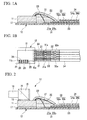
FIG. 1A is a cross-sectional view showing a first embodiment of a substrate with an imaging device chip mounted thereon according to the invention. -
FIG. 1B is a plan view showing the first embodiment of the substrate with the imaging device chip mounted thereon according to the invention. -
FIG. 2 is a cross-sectional view showing an example of an imaging module in which a lens and a prism are provided on the imaging device chip ofFIGS. 1A and 1B . -
FIG. 3 is a front view when the imaging module ofFIG. 2 is viewed from the side facing the lens. -
FIG. 4A is a plan view showing an example of an endoscope. -
FIG. 4B is a cross-sectional view showing an example of a scope tip portion. -
FIG. 5 is a front view showing an example in which the imaging module ofFIG. 2 is inserted into the scope tip portion. -
FIG. 6 is a perspective view showing an example in which the scope tip portion ofFIG. 5 is sealed with resin. -
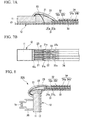
FIG. 7A is a cross-sectional view showing a second embodiment of the substrate with the imaging device chip mounted thereon according to the invention. -
FIG. 7B is a plan view showing the second embodiment of the substrate with the imaging device chip mounted thereon according to the invention. -
FIG. 8 is a cross-sectional view showing an example of an imaging module in which a lens is provided on the imaging device chip ofFIGS. 7A and 7B . - Hereinafter, the invention will be described based on preferred embodiments with reference to the drawings.
-
FIGS. 1A and 1B show a first embodiment of asubstrate 12 with animaging device chip 11 mounted thereon according to the invention. - As the
imaging device chip 11, although it is not particularly limited, a semiconductor chip such as a CMOS (complementary metal oxide semiconductor), a CCD (charge-coupled device), or a CPD (charge priming device) can be provided. The size of the chip is not particularly limited. However, in order to reduce the diameter of a tube which is used in an endoscope, it is preferable to adopt a small-sized chip, and it is also possible to use a chip having sides (a long side and a short side) less than or equal to about 2 mm and a thickness less than or equal to about 0.5 mm, for example. - As for the
substrate 12, a flexible substrate is used such that it is possible to bend thesubstrate 12 when thesubstrate 12 is inserted into atubular housing tube 2 in ascope tip portion 3 of an endoscope 1, as shown inFIGS. 4B and5 . - As the
flexible substrate 12, a flexible wiring board (FPC) with a metal layer such as copper foil formed on one face or both faces of a flexible insulating film, or a laminated wiring board in which two or more FPCs are laminated is preferable. As the insulating film, polyimide, polyester, liquid crystal polymer, or the like can be used. However, it is not particularly limited thereto. For example, it is possible that the thickness of thesubstrate 12 is set to be in a range of 50 to 200 µm, for example. - In the case of the first embodiment, a plurality of
FPCs films adhesive layer 33 interposed therebetween, and connection portions (first substrate connection portions) 31a and 32a formed by patterning metal layers of theFPCs substrate 12, compared to a pitch of a connection portion (a first chip connection portion) 11a of theimaging device chip 11. A coverlay 34 (a protective film) in which anadhesive layer 34b is formed on one face of an insulatingfilm 34a is laminated on theFPC 32 of the uppermost layer. - In a method of packaging the
imaging device chip 11 according to the first embodiment, first, theimaging device chip 11 is fixed to thesubstrate 12. A member fixing theimaging device chip 11 to thesubstrate 12 is not particularly limited, and ajointing material 17 such as an adhesive, solder, or silver solder, a mechanical member such as a screw, or the like can be used appropriately. - After the fixation of the
imaging device chip 11, the connection portions (the first chip connection portions) 11a of theimaging device chip 11 and the connection portions (the first substrate connection portions) 31a and 32a of thesubstrate 12 are connected by lead wires (first lead wires) 21 and 22. Furthermore, connection portions (second chip connection portions) 11b of theimaging device chip 11 and connection portions (second substrate connection portions) 26 of thesubstrate 12 are connected by lead wires (second lead wires) 24. Theconnection portions imaging device chip 11. Furthermore, theconnection portions substrate 12 are terminals such as pads formed at wirings of thesubstrate 12. As thelead wires - At the time of the connection using the
lead wires substrate 12 may have a shape arbitrarily determined depending on an imaging module of an endoscope, for example, a planar shape. For this reason, it is possible to efficiently proceed with work by using an automatic wire-bonding apparatus. - In the case of the first embodiment, the
imaging device chip 11 has the first connection portions (the first chip connection portions) 11a arranged along the short side which is located at an end (the right side inFIG. 1B ) in a longitudinal direction of thescope tip portion 3, and the second connection portions (the second chip connection portions) 11b arranged along the long side which is located at an end (the lower side inFIG. 1B ) orthogonal to the longitudinal direction of thescope tip portion 3. - The connection portions of the
substrate 12 have the first connection portions (the first substrate connection portions) 31a and 32a which are located in a direction (inFIG. 1B , the right-and-left direction) along the longitudinal direction of thescope tip portion 3 with respect to the first connection portions (the first chip connection portions) 11a of theimaging device chip 11, and the second connection portions (the second substrate connection portions) 26 which are located in a direction (inFIG. 1B , the up-and-down direction) orthogonal to the longitudinal direction of thescope tip portion 3 with respect to the second connection portions (the second chip connection portions) 11b of theimaging device chip 11. - The first connection portions (the first chip connection portions) 11a of the
imaging device chip 11 and the first connection portions (the first substrate connection portions) 31a and 32a of thesubstrate 12 are connected by thefirst lead wires scope tip portion 3. - Furthermore, the second connection portions (the second chip connection portions) 11b of the
imaging device chip 11 and the second connection portions (the second substrate connection portions) 26 of thesubstrate 12 are connected by thesecond lead wires 24 extending substantially in the direction orthogonal to the longitudinal direction of thescope tip portion 3. - In this way, even if the
imaging device chip 11 is provided with a large number ofconnection portions first connection portions 11a and thesecond connection portions 11b are provided along two orthogonal sides of theimaging device chip 11, therespective lead wires substrate 12 without being congested. - After the first chip connection portions and the first substrate connection portions are connected by the
lead wires lead wires non-conductive resin 23. Furthermore, after the second chip connection portions and the second substrate connection portions are connected by thelead wires 24, the entirety of thelead wires 24 is covered with flexible andnon-conductive resin 25. In this way, the contact between thelead wires resins connection portions substrate 12 and theconnection portions imaging device chip 11, whereby connection places between these connection portions and thelead wires - An
imaging module 10 according to the first embodiment shown inFIG. 2 is provided with aprism 14 fixed onto theimaging device chip 11 and anobjective lens 13 mounted on theprism 14, as an optical system for forming an optical image on an imaging area of theimaging device chip 11. Theprism 14 has a supportingmember 15 mounted thereon and is fixed to aperiphery 16 of the imaging area in theimaging device chip 11 by an adhesive or the like. - The
objective lens 13 may be a column-shaped gradient index lens (GRIN lens) and may also have a structure in which alens 19 is mounted in aframe 20, as shown inFIG. 8 . - In addition, mounting of the
prism 14 or theobjective lens 13 may be performed after theimaging device chip 11 is mounted on thesubstrate 12 and may be performed before theimaging device chip 11 is mounted on thesubstrate 12. - According to the method of packaging the
imaging device chip 11 related to the first embodiment, since theconnection portions substrate 12 and theconnection portions 11a of theimaging device chip 11 are connected by theflexible lead wires connection portions substrate 12 and theconnection portions 11a of theimaging device chip 11 is covered with the flexible andnon-conductive resin 23, it is possible to bend thesubstrate 12. - In addition, since the
connection portions 26 of thesubstrate 12 and theconnection portions 11b of theimaging device chip 11 are connected by theflexible lead wires 24 and an area between theconnection portions 26 of thesubstrate 12 and theconnection portions 11b of theimaging device chip 11 is covered with the flexible andnon-conductive resin 25, it is possible to bend thesubstrate 12. - In the case of the
imaging module 10 according to the first embodiment, it is possible to bend thesubstrate 12 to be directed to the longitudinal direction between the first connection portions (the first substrate connection portions) 31a and 32a of thesubstrate 12 and the first connection portions (the first chip connection portions) 11a of the imaging device chip 11 (at an area which includes the first substrate connection portions and the first chip connection portions, at near the first substrate connection portions) (refer toFIG. 8 ). In addition, it is possible to bend thesubstrate 12 to be directed to the direction orthogonal to the longitudinal direction between the second connection portions (the second substrate connection portions) 26 of thesubstrate 12 and the second connection portions (the second chip connection portions) 11b of the imaging device chip 11 (at an area which includes the second substrate connection portions and the second chip connection portions, at near the second substrate connection portions). - It is preferable that the flexible and
non-conductive resins - The
imaging module 10 shown inFIG. 2 can be used while being inserted into thehousing tube 2 in thescope tip portion 3 of the endoscope 1, as shown inFIG. 4B . Theflexible substrate 12 may be connected to an electric signal line 4 such as a cord or a cable on the way. In the endoscope 1 shown inFIG. 4A , a connector (an electric connector) 5 is provided at an end portion on the side where an operator manipulates the endoscope 1, and the electric signal line 4 is electrically connected to a terminal (not shown) in the connector 5. In this way, it is possible to connect the electric signal line 4 of the endoscope 1 to an image display device such as a video processor or a personal computer immediately. - As the electric signal line 4, although it is not particularly limited, an ultrafine coaxial cable (for example, a coaxial cable in which the size of a central conductor is less than or equal to 36 in AWG (American Wire Gauge) standard) is preferable. As the connector 5, although it is not particularly limited, various standards such as a USB (Universal Serial Bus) are widely known and any of them can be suitably used in the invention.
-
FIG. 5 shows a state where thesubstrate 12 of theimaging module 10 is inserted into thehousing tube 2 while bending thesubstrate 12 to be directed to a direction orthogonal to the longitudinal direction of thescope tip portion 3. Thesubstrate 12 is inserted into thehousing tube 2 along with thelead wires 24 connected to thesecond connection portions 26 of thesubstrate 12, while bending thesubstrate 12 to be directed to the direction orthogonal to the longitudinal direction (inFIG. 5 , a direction perpendicular to the plane of paper) of thescope tip portion 3. In this way, compared to a case where a substrate is not bent, the width of thesubstrate 12 in the direction orthogonal to the longitudinal direction of thescope tip portion 3 can be reduced, and thus it is possible to use thehousing tube 2 having a smaller inner diameter. In addition, in theimaging module 10 before it is inserted into thehousing tube 2, thesubstrate 12 may be flat, as shown inFIG. 3 . - In the first embodiment, since an optical path changing member such as a prism is provided on the
imaging module 10 and the imaging area of theimaging module 10 is directed in the direction (inFIG. 5 , an upward direction) orthogonal to the longitudinal direction of thescope tip portion 3, even if the inner diameter of thehousing tube 2 is slightly larger than the length of a side of theimaging device chip 11, the insertion of theimaging module 10 becomes possible. That is, in the first embodiment of the invention, it is possible to use a housing tube having a small inner diameter. On the other hand, as in Patent Document 1 (Japanese Patent No.3216650 imaging module 10 is directed in the longitudinal direction of thescope tip portion 3, in order to accommodate theimaging device chip 11, the inner diameter of thehousing tube 2 needs to be larger than the length of a diagonal of the imaging device chip 11 (the length of a diagonal of theimaging device chip 11 when theimaging device chip 11 is viewed from above, as shown inFIG. 1B ). -
FIG. 6 shows a state where a tip portion of thehousing tube 2 is sealed with a sealingmaterial 6 after theimaging module 10 is inserted into thehousing tube 2. Theobjective lens 13 is exposed at thescope tip portion 3. In order to prevent the sealingmaterial 6 from invading onto the object plane of theobjective lens 13, it is also possible to make a configuration so as to dam up the sealingmaterial 6 by making an end portion of atube 18 protrude around theobjective lens 13. - The invention has been described above based on the preferred first embodiment. However, the invention is not limited to the first embodiment described above and various modifications are possible within a scope which does not depart from the invention.
-
FIGS. 7A and 7B show a second embodiment of thesubstrate 12 with theimaging device chip 11 mounted thereon, in the invention. - In the case of the second embodiment, the
connection portions substrate 12 are located in the direction (inFIG. 7B , the right-and-left direction) along the longitudinal direction of thescope tip portion 3 with respect to theconnection portions 11 a of theimaging device chip 11. Theconnection portions 11a of theimaging device chip 11 and theconnection portions substrate 12 are connected by thelead wires scope tip portion 3. - In a method of packaging the
imaging device chip 11 according to the second embodiment, similar to the first embodiment, theimaging device chip 11 is fixed to thesubstrate 12, theconnection portions substrate 12 and theconnection portions 11a of theimaging device chip 11 are connected by thelead wires lead wires non-conductive resin 23. - In this way, the contact between the
lead wires resin 23 includes theconnection portions substrate 12 and theconnection portions 11a of theimaging device chip 11, whereby connection places between these connection portions and thelead wires - Furthermore, since the
connection portions substrate 12 and theconnection portions 11a of theimaging device chip 11 are connected by theflexible lead wires connection portions substrate 12 and theconnection portions 11a of the imaging device chip 11 (an area which includes the substrate connection portions and the chip connection portions, at near the substrate connection portions) is covered with the flexible andnon-conductive resin 23, it is possible to bend thesubstrate 12. - In this way, in comparison with a method in which the connection of a lead frame is performed in a state where a connection substrate is bent, as described in Paragraph 0040 of Patent Document 1 (Japanese Patent No.
3216650 flexible lead wires flexible substrate 12 being flat, and thus it is possible to improve productivity. - In an
imaging module 10A according to a third embodiment shown inFIG. 8 , as an optical system for forming an optical image on the imaging area of theimaging device chip 11, thelens 19 is mounted in theframe 20 and then fixed onto theimaging device chip 11. - In the
imaging module 10A according to the third embodiment, it is possible to insert thesubstrate 12 into a housing tube (not shown) in a scope tip portion of an endoscope while bending thesubstrate 12 to be directed to the longitudinal direction between thefirst connection portions substrate 12 and theconnection portions 11a of the imaging device chip 11 (at an area which includes the substrate connection portions and the chip connection portions, in near the substrate connection portions). - A method of configuring an endoscope by using the
imaging module 10A according to a fourth embodiment can be carried out in the same manner as in the case using theimaging module 10 according to the first embodiment. For example, as shown inFIG. 6 , it is also possible to seal the tip portion of the housing tube around the objective lens by using a sealing material after the imaging module is inserted into the housing tube. - According to the
imaging module 10A related to the fourth embodiment, since it is possible to bend thesubstrate 12 even after theconnection portions substrate 12 and theconnection portions 11a of theimaging device chip 11 are connected and covered with theresin 23, it is possible to insert thesubstrate 12 into the scope tip portion having a smaller diameter, and thus it is possible to reduce the diameter of the endoscope with a simpler configuration.
Claims (8)
- An endoscope comprising:an imaging device chip having a chip connection portion;a tubular housing tube used to a scope tip portion of an endoscope;a substrate to which the imaging device chip is fixed, the substrate having a substrate connection portion, the substrate being capable of bending at near the substrate connection portion when the substrate is inserted into the housing tube;a lead wire connecting the substrate connection portion and the chip connection portion;flexible and non-conductive resin covering an entirety of the lead wire; andan imaging module comprising the substrate provided with the imaging device chip thereon, the imaging module being inserted into the housing tube.
- An imaging module inserted into a tubular housing tube in a scope tip portion of an endoscope, comprising:an imaging device chip having a chip connection portion;a substrate to which the imaging device chip is fixed, the substrate having a substrate connection portion, the substrate being capable of bending at near the substrate connection portion when the substrate is inserted into the housing tube, ;a lead wire connecting the substrate connection portion and the chip connection portion; andflexible and non-conductive resin covering an entirety of the lead wire.
- A method of assembling an endoscope comprising:preparing an imaging device chip having a chip connection portion, a tubular housing tube used as a scope tip portion of an endoscope, and a substrate having a substrate connection portion, the substrate being capable of bending at near the substrate connection portion when the substrate is inserted into the housing tube;fixing the imaging device chip to the substrate;connecting the substrate connection portion and the chip connection portion by a lead wire;covering an entirety of the lead wire with flexible and non-conductive resin; andbending the substrate, to which the imaging device chip is fixed, at near the substrate connection portion, and thereby inserting the substrate into the housing tube.
- The method of assembling an endoscope according to Claim 3, further comprising:arranging the substrate connection portion in a direction along a longitudinal direction of the scope tip portion with respect to the chip connection portion; andbending the substrate at near the substrate connection portion to be directed to the longitudinal direction, and thereby inserting the substrate into the housing tube.
- The method of assembling an endoscope according to Claim 3, wherein the substrate connection portion has a first substrate connection portion and a second substrate connection portion,
the chip connection portion has a first chip connection portion and a second chip connection portion,
the lead wire has a first lead wire and a second lead wire,
the method further comprises:arranging the first substrate connection portion in a direction along a longitudinal direction of the scope tip portion with respect to the first chip connection portion;arranging the second substrate connection portion in a direction orthogonal to the longitudinal direction of the scope tip portion with respect to the second chip connection portion;connecting the first substrate connection portion and the first chip connection portion by the first lead wire;covering an entirety of the first lead wire with flexible and non-conductive resin;connecting the second substrate connection portion and the second chip connection portion by the second lead wire,covering an entirety of the second lead wire with flexible and non-conductive resin, andbending the substrate at near the second substrate connection portion to be directed to the orthogonal direction, thereby inserting the substrate into the housing tube. - A method of packaging an imaging device chip inserted into a tubular housing tube in a scope tip portion of an endoscope, comprising:preparing an imaging device chip having a chip connection portion, and a substrate having a substrate connection portion, the substrate being capable of bending at near the substrate connection portion when the substrate is inserted into the housing tube;fixing the imaging device chip to the substrate;connecting the substrate connection portion and the chip connection portion by a lead wire; andcovering an entirety of the lead wire with flexible and non-conductive resin.
- The method of packaging an imaging device chip according to Claim 6, further comprising arranging the substrate connection portion in a direction along a longitudinal direction of the scope tip portion with respect to the chip connection portion.
- The method of packaging an imaging device chip according to Claim 6, wherein the substrate connection portion has a first substrate connection portion and a second substrate connection portion,
the chip connection portion has a first chip connection portion and a second chip connection portion,
the lead wire has a first lead wire and a second lead wire,
the method further comprises:arranging the first substrate connection portion in a direction along a longitudinal direction of the scope tip portion with respect to the first chip connection portion,arranging the second substrate connection portion in a direction orthogonal to the longitudinal direction of the scope tip portion with respect to the second chip connection portion,connecting the first substrate connection portion and the first chip connection portion by the first lead wire,covering an entirety of the first lead wire with flexible and non-conductive resin,connecting the second substrate connection portion and the second chip connection portion by the second lead wire, andcovering an entirety of the second lead wire with flexible and non-conductive resin.
Applications Claiming Priority (2)
| Application Number | Priority Date | Filing Date | Title |
|---|---|---|---|
| JP2011249755A JP5386567B2 (en) | 2011-11-15 | 2011-11-15 | Imaging device chip mounting method, endoscope assembling method, imaging module, and endoscope |
| PCT/JP2012/079522 WO2013073578A1 (en) | 2011-11-15 | 2012-11-14 | Image capture element chip mounting method, endoscope assembly method, image capture module, and endoscope |
Publications (3)
| Publication Number | Publication Date |
|---|---|
| EP2781183A1 true EP2781183A1 (en) | 2014-09-24 |
| EP2781183A4 EP2781183A4 (en) | 2015-08-12 |
| EP2781183B1 EP2781183B1 (en) | 2018-02-21 |
Family
ID=48429633
Family Applications (1)
| Application Number | Title | Priority Date | Filing Date |
|---|---|---|---|
| EP12849196.6A Not-in-force EP2781183B1 (en) | 2011-11-15 | 2012-11-14 | Image capture element chip mounting method, endoscope assembly method, image capture module, and endoscope |
Country Status (5)
| Country | Link |
|---|---|
| US (1) | US10510918B2 (en) |
| EP (1) | EP2781183B1 (en) |
| JP (1) | JP5386567B2 (en) |
| CN (1) | CN103889308A (en) |
| WO (1) | WO2013073578A1 (en) |
Cited By (2)
| Publication number | Priority date | Publication date | Assignee | Title |
|---|---|---|---|---|
| WO2017127597A1 (en) * | 2016-01-21 | 2017-07-27 | Littelfuse, Inc. | Surface mounted protection device |
| EP3518519A1 (en) * | 2018-01-26 | 2019-07-31 | Fujikura Ltd. | Imaging module |
Families Citing this family (20)
| Publication number | Priority date | Publication date | Assignee | Title |
|---|---|---|---|---|
| US20150229813A1 (en) * | 2013-02-11 | 2015-08-13 | Oran Jacob Isaac-Lowry | Miniature High Definition Camera System |
| US9257763B2 (en) | 2013-07-02 | 2016-02-09 | Gyrus Acmi, Inc. | Hybrid interconnect |
| US9510739B2 (en) | 2013-07-12 | 2016-12-06 | Gyrus Acmi, Inc. | Endoscope small imaging system |
| EP2923635A4 (en) * | 2013-10-04 | 2016-12-21 | Olympus Corp | Image pickup unit for endoscope |
| WO2015057257A1 (en) * | 2013-10-15 | 2015-04-23 | Jil Holdings Llc | Miniature high definition camera system |
| US9591758B2 (en) | 2014-03-27 | 2017-03-07 | Intel Corporation | Flexible electronic system with wire bonds |
| JP6431698B2 (en) * | 2014-06-16 | 2018-11-28 | オリンパス株式会社 | Imaging unit, wiring board with cable, and method of manufacturing wiring board with cable |
| WO2016117123A1 (en) | 2015-01-23 | 2016-07-28 | オリンパス株式会社 | Image-capturing device and endoscope |
| KR102481003B1 (en) * | 2015-04-27 | 2022-12-26 | 엘지이노텍 주식회사 | Camera module |
| CN106358360B (en) | 2015-07-14 | 2019-07-19 | 财团法人工业技术研究院 | Flexible electronic device and method of making the same |
| US11647678B2 (en) | 2016-08-23 | 2023-05-09 | Analog Devices International Unlimited Company | Compact integrated device packages |
| US10629574B2 (en) * | 2016-10-27 | 2020-04-21 | Analog Devices, Inc. | Compact integrated device packages |
| JP6776840B2 (en) * | 2016-11-21 | 2020-10-28 | オムロン株式会社 | Electronic devices and their manufacturing methods |
| EP3795076B1 (en) | 2018-01-31 | 2023-07-19 | Analog Devices, Inc. | Electronic devices |
| WO2020097361A1 (en) * | 2018-11-07 | 2020-05-14 | Meditrina, Inc. | Endoscope and method of use |
| WO2020173555A1 (en) * | 2019-02-26 | 2020-09-03 | Zeronoise Ltd | Apparatus to acquire and process images for a helmet, corresponding helmet and method to acquire and process images |
| WO2021149177A1 (en) * | 2020-01-22 | 2021-07-29 | オリンパス株式会社 | Imaging device, endoscope, and method for manufacturing imaging device |
| US11153970B1 (en) | 2020-07-20 | 2021-10-19 | Atl Technology, Llc | Apparatus with electrical components end mounted to printed circuit board |
| US11735879B2 (en) | 2021-03-09 | 2023-08-22 | Atl Technology, Llc | Adaptor for converting a ball grid array interface into a pin interface |
| US12177989B2 (en) | 2021-11-16 | 2024-12-24 | Atl Technology, Llc | Direct wire attachment methods and apparatus for a BGA component |
Family Cites Families (31)
| Publication number | Priority date | Publication date | Assignee | Title |
|---|---|---|---|---|
| JPS6077731A (en) * | 1983-10-03 | 1985-05-02 | オリンパス光学工業株式会社 | Endoscope apparatus using solid-image pick-up element |
| JPS6150544A (en) | 1984-08-20 | 1986-03-12 | オリンパス光学工業株式会社 | Endoscope |
| JPH0629911B2 (en) | 1985-05-07 | 1994-04-20 | 旭光学工業株式会社 | End tip structure of endoscope |
| JP3216650B2 (en) | 1990-08-27 | 2001-10-09 | オリンパス光学工業株式会社 | Solid-state imaging device |
| US5418566A (en) * | 1990-09-10 | 1995-05-23 | Kabushiki Kaisha Toshiba | Compact imaging apparatus for electronic endoscope with improved optical characteristics |
| JPH0969983A (en) * | 1995-08-30 | 1997-03-11 | Matsushita Electric Ind Co Ltd | Solid-state imaging device |
| JP3623311B2 (en) * | 1996-05-17 | 2005-02-23 | オリンパス株式会社 | Solid-state imaging device |
| DE19924189C2 (en) * | 1999-05-27 | 2001-04-26 | Storz Karl Gmbh & Co Kg | Image sensor module and method for assembling such an image sensor module |
| JP2001051210A (en) * | 1999-08-05 | 2001-02-23 | Asahi Optical Co Ltd | Electronic endoscope |
| JP2001053988A (en) * | 1999-08-06 | 2001-02-23 | Asahi Optical Co Ltd | Flexible printed circuit board for wiring of electronic endoscope |
| JP4071580B2 (en) * | 2002-09-02 | 2008-04-02 | 株式会社フジクラ | Image fiber processing method |
| JP5030360B2 (en) * | 2002-12-25 | 2012-09-19 | オリンパス株式会社 | Method for manufacturing solid-state imaging device |
| US8118732B2 (en) * | 2003-04-01 | 2012-02-21 | Boston Scientific Scimed, Inc. | Force feedback control system for video endoscope |
| WO2005067783A1 (en) * | 2004-01-19 | 2005-07-28 | Olympus Corporation | Imaging device for endoscope and capsule type endoscope |
| DE602005021052D1 (en) * | 2004-01-19 | 2010-06-17 | Olympus Corp | MEDICAL TREATMENT DEVICE OF CAPSULE TYPE |
| JP2005295050A (en) * | 2004-03-31 | 2005-10-20 | Miyota Kk | Camera module |
| TWI264224B (en) * | 2004-07-28 | 2006-10-11 | Fujitsu Ltd | Imaging apparatus |
| US8858425B2 (en) * | 2004-09-24 | 2014-10-14 | Vivid Medical, Inc. | Disposable endoscope and portable display |
| JP4812050B2 (en) * | 2004-12-17 | 2011-11-09 | 株式会社日立メディコ | Ultrasonic probe and ultrasonic diagnostic apparatus using the same |
| JP5422121B2 (en) * | 2005-08-04 | 2014-02-19 | 日亜化学工業株式会社 | LIGHT EMITTING DEVICE, ITS MANUFACTURING METHOD, MOLDED BODY, AND SEALING MEMBER |
| JP4855168B2 (en) * | 2006-07-27 | 2012-01-18 | オリンパス株式会社 | Solid-state imaging device |
| JP2008109378A (en) * | 2006-10-25 | 2008-05-08 | Matsushita Electric Ind Co Ltd | Optical device module and manufacturing method thereof, and optical device unit and manufacturing method thereof |
| JP4682158B2 (en) * | 2007-01-16 | 2011-05-11 | オリンパスメディカルシステムズ株式会社 | Imaging device |
| JP2009082504A (en) | 2007-09-28 | 2009-04-23 | Fujifilm Corp | Imaging apparatus and endoscope provided with the imaging apparatus |
| JP5289870B2 (en) | 2008-09-08 | 2013-09-11 | オリンパスメディカルシステムズ株式会社 | Endoscope imaging unit |
| CN102802497B (en) * | 2009-06-25 | 2015-03-25 | 奥林巴斯医疗株式会社 | Image Pickup Unit |
| JP5452273B2 (en) * | 2010-02-15 | 2014-03-26 | オリンパス株式会社 | Semiconductor device |
| JP2011212161A (en) * | 2010-03-31 | 2011-10-27 | Fujifilm Corp | Solid-state image pickup device and endoscopic device |
| US8698887B2 (en) * | 2010-04-07 | 2014-04-15 | Olympus Corporation | Image pickup apparatus, endoscope and manufacturing method for image pickup apparatus |
| JP5586402B2 (en) * | 2010-09-29 | 2014-09-10 | 富士フイルム株式会社 | Endoscope apparatus and imaging element heat dissipation method thereof |
| JP5436470B2 (en) | 2011-01-31 | 2014-03-05 | 富士フイルム株式会社 | Imaging device and electronic endoscope provided with the same |
-
2011
- 2011-11-15 JP JP2011249755A patent/JP5386567B2/en not_active Expired - Fee Related
-
2012
- 2012-11-14 CN CN201280053046.9A patent/CN103889308A/en active Pending
- 2012-11-14 EP EP12849196.6A patent/EP2781183B1/en not_active Not-in-force
- 2012-11-14 WO PCT/JP2012/079522 patent/WO2013073578A1/en not_active Ceased
-
2014
- 2014-05-12 US US14/275,214 patent/US10510918B2/en active Active
Cited By (4)
| Publication number | Priority date | Publication date | Assignee | Title |
|---|---|---|---|---|
| WO2017127597A1 (en) * | 2016-01-21 | 2017-07-27 | Littelfuse, Inc. | Surface mounted protection device |
| US10283304B2 (en) | 2016-01-21 | 2019-05-07 | Littelfuse, Inc. | Surface mounted protection device |
| EP3518519A1 (en) * | 2018-01-26 | 2019-07-31 | Fujikura Ltd. | Imaging module |
| US10888217B2 (en) | 2018-01-26 | 2021-01-12 | Fujikura Ltd. | Imaging module applicable to head-swing endoscope |
Also Published As
| Publication number | Publication date |
|---|---|
| WO2013073578A1 (en) | 2013-05-23 |
| CN103889308A (en) | 2014-06-25 |
| JP5386567B2 (en) | 2014-01-15 |
| US10510918B2 (en) | 2019-12-17 |
| EP2781183B1 (en) | 2018-02-21 |
| US20140249368A1 (en) | 2014-09-04 |
| EP2781183A4 (en) | 2015-08-12 |
| JP2013103011A (en) | 2013-05-30 |
Similar Documents
| Publication | Publication Date | Title |
|---|---|---|
| EP2781183B1 (en) | Image capture element chip mounting method, endoscope assembly method, image capture module, and endoscope | |
| EP2944248B1 (en) | Manufacturing method of semiconductor apparatus, semiconductor apparatus, and endoscope | |
| CN113163595A (en) | Chip on film, roll and display device | |
| CN111355036B (en) | Cable assembly, cable holder, and method of manufacturing a cable assembly | |
| US8488928B2 (en) | Opto-electro hybrid harness and method of manufacturing the same | |
| EP2905954A1 (en) | Imaging device, and endoscope provided with said imaging device | |
| US10211551B2 (en) | Electronic circuit module | |
| JP4910721B2 (en) | Connection structure of multi-core cable, multi-core cable with connector and multi-core cable | |
| CN101681693A (en) | Cable harness, cable harness with connector, and connection structure of cable harness | |
| US9774151B2 (en) | Cable connection structure | |
| CN106031150A (en) | Imaging device, and method for manufacturing imaging device | |
| CN105814743A (en) | Contact connecting of shielded data lines to a board and method for contacting a number of shielded data lines with a board | |
| JP6081170B2 (en) | Imaging apparatus, endoscope, and manufacturing method of imaging apparatus | |
| US10321814B2 (en) | Image pickup apparatus and endoscope | |
| JP6689908B2 (en) | Imaging module | |
| JP6188479B2 (en) | Board module | |
| US8513536B2 (en) | Electronic circuit module and method of connecting coaxial cable | |
| JPH08172177A (en) | Solid-state image pickup module and endoscope apparatus | |
| US10888217B2 (en) | Imaging module applicable to head-swing endoscope | |
| JP2009037773A (en) | Connector, cable connecting structure, electronic device and connecting method of connector and base board | |
| JP2022015876A (en) | Connection structure and photo-electric hybrid substrate used for the same | |
| WO2020137384A1 (en) | Imaging module | |
| JP4209762B2 (en) | Imaging device | |
| US20240087771A1 (en) | Cable connection structure and method for manufacturing cable connection structure | |
| JPH08172176A (en) | Solid-state image pickup module and endoscope apparatus |
Legal Events
| Date | Code | Title | Description |
|---|---|---|---|
| PUAI | Public reference made under article 153(3) epc to a published international application that has entered the european phase |
Free format text: ORIGINAL CODE: 0009012 |
|
| 17P | Request for examination filed |
Effective date: 20140512 |
|
| AK | Designated contracting states |
Kind code of ref document: A1 Designated state(s): AL AT BE BG CH CY CZ DE DK EE ES FI FR GB GR HR HU IE IS IT LI LT LU LV MC MK MT NL NO PL PT RO RS SE SI SK SM TR |
|
| DAX | Request for extension of the european patent (deleted) | ||
| RA4 | Supplementary search report drawn up and despatched (corrected) |
Effective date: 20150709 |
|
| RIC1 | Information provided on ipc code assigned before grant |
Ipc: H04N 5/225 20060101ALI20150703BHEP Ipc: H04N 5/335 20110101ALI20150703BHEP Ipc: A61B 1/04 20060101AFI20150703BHEP Ipc: A61B 1/00 20060101ALI20150703BHEP Ipc: G02B 23/24 20060101ALI20150703BHEP Ipc: H01L 31/18 20060101ALI20150703BHEP Ipc: A61B 1/05 20060101ALI20150703BHEP Ipc: H01L 31/0203 20140101ALI20150703BHEP |
|
| 17Q | First examination report despatched |
Effective date: 20170123 |
|
| GRAP | Despatch of communication of intention to grant a patent |
Free format text: ORIGINAL CODE: EPIDOSNIGR1 |
|
| INTG | Intention to grant announced |
Effective date: 20170922 |
|
| GRAS | Grant fee paid |
Free format text: ORIGINAL CODE: EPIDOSNIGR3 |
|
| GRAA | (expected) grant |
Free format text: ORIGINAL CODE: 0009210 |
|
| AK | Designated contracting states |
Kind code of ref document: B1 Designated state(s): AL AT BE BG CH CY CZ DE DK EE ES FI FR GB GR HR HU IE IS IT LI LT LU LV MC MK MT NL NO PL PT RO RS SE SI SK SM TR |
|
| REG | Reference to a national code |
Ref country code: GB Ref legal event code: FG4D |
|
| REG | Reference to a national code |
Ref country code: CH Ref legal event code: EP |
|
| REG | Reference to a national code |
Ref country code: DE Ref legal event code: R096 Ref document number: 602012043191 Country of ref document: DE Ref country code: AT Ref legal event code: REF Ref document number: 970794 Country of ref document: AT Kind code of ref document: T Effective date: 20180315 |
|
| REG | Reference to a national code |
Ref country code: IE Ref legal event code: FG4D |
|
| REG | Reference to a national code |
Ref country code: NL Ref legal event code: MP Effective date: 20180221 |
|
| REG | Reference to a national code |
Ref country code: LT Ref legal event code: MG4D |
|
| REG | Reference to a national code |
Ref country code: AT Ref legal event code: MK05 Ref document number: 970794 Country of ref document: AT Kind code of ref document: T Effective date: 20180221 |
|
| PG25 | Lapsed in a contracting state [announced via postgrant information from national office to epo] |
Ref country code: FI Free format text: LAPSE BECAUSE OF FAILURE TO SUBMIT A TRANSLATION OF THE DESCRIPTION OR TO PAY THE FEE WITHIN THE PRESCRIBED TIME-LIMIT Effective date: 20180221 Ref country code: CY Free format text: LAPSE BECAUSE OF FAILURE TO SUBMIT A TRANSLATION OF THE DESCRIPTION OR TO PAY THE FEE WITHIN THE PRESCRIBED TIME-LIMIT Effective date: 20180221 Ref country code: LT Free format text: LAPSE BECAUSE OF FAILURE TO SUBMIT A TRANSLATION OF THE DESCRIPTION OR TO PAY THE FEE WITHIN THE PRESCRIBED TIME-LIMIT Effective date: 20180221 Ref country code: NL Free format text: LAPSE BECAUSE OF FAILURE TO SUBMIT A TRANSLATION OF THE DESCRIPTION OR TO PAY THE FEE WITHIN THE PRESCRIBED TIME-LIMIT Effective date: 20180221 Ref country code: ES Free format text: LAPSE BECAUSE OF FAILURE TO SUBMIT A TRANSLATION OF THE DESCRIPTION OR TO PAY THE FEE WITHIN THE PRESCRIBED TIME-LIMIT Effective date: 20180221 Ref country code: NO Free format text: LAPSE BECAUSE OF FAILURE TO SUBMIT A TRANSLATION OF THE DESCRIPTION OR TO PAY THE FEE WITHIN THE PRESCRIBED TIME-LIMIT Effective date: 20180521 Ref country code: HR Free format text: LAPSE BECAUSE OF FAILURE TO SUBMIT A TRANSLATION OF THE DESCRIPTION OR TO PAY THE FEE WITHIN THE PRESCRIBED TIME-LIMIT Effective date: 20180221 |
|
| PG25 | Lapsed in a contracting state [announced via postgrant information from national office to epo] |
Ref country code: BG Free format text: LAPSE BECAUSE OF FAILURE TO SUBMIT A TRANSLATION OF THE DESCRIPTION OR TO PAY THE FEE WITHIN THE PRESCRIBED TIME-LIMIT Effective date: 20180521 Ref country code: AT Free format text: LAPSE BECAUSE OF FAILURE TO SUBMIT A TRANSLATION OF THE DESCRIPTION OR TO PAY THE FEE WITHIN THE PRESCRIBED TIME-LIMIT Effective date: 20180221 Ref country code: SE Free format text: LAPSE BECAUSE OF FAILURE TO SUBMIT A TRANSLATION OF THE DESCRIPTION OR TO PAY THE FEE WITHIN THE PRESCRIBED TIME-LIMIT Effective date: 20180221 Ref country code: LV Free format text: LAPSE BECAUSE OF FAILURE TO SUBMIT A TRANSLATION OF THE DESCRIPTION OR TO PAY THE FEE WITHIN THE PRESCRIBED TIME-LIMIT Effective date: 20180221 Ref country code: RS Free format text: LAPSE BECAUSE OF FAILURE TO SUBMIT A TRANSLATION OF THE DESCRIPTION OR TO PAY THE FEE WITHIN THE PRESCRIBED TIME-LIMIT Effective date: 20180221 Ref country code: GR Free format text: LAPSE BECAUSE OF FAILURE TO SUBMIT A TRANSLATION OF THE DESCRIPTION OR TO PAY THE FEE WITHIN THE PRESCRIBED TIME-LIMIT Effective date: 20180522 |
|
| PG25 | Lapsed in a contracting state [announced via postgrant information from national office to epo] |
Ref country code: PL Free format text: LAPSE BECAUSE OF FAILURE TO SUBMIT A TRANSLATION OF THE DESCRIPTION OR TO PAY THE FEE WITHIN THE PRESCRIBED TIME-LIMIT Effective date: 20180221 Ref country code: EE Free format text: LAPSE BECAUSE OF FAILURE TO SUBMIT A TRANSLATION OF THE DESCRIPTION OR TO PAY THE FEE WITHIN THE PRESCRIBED TIME-LIMIT Effective date: 20180221 Ref country code: RO Free format text: LAPSE BECAUSE OF FAILURE TO SUBMIT A TRANSLATION OF THE DESCRIPTION OR TO PAY THE FEE WITHIN THE PRESCRIBED TIME-LIMIT Effective date: 20180221 Ref country code: AL Free format text: LAPSE BECAUSE OF FAILURE TO SUBMIT A TRANSLATION OF THE DESCRIPTION OR TO PAY THE FEE WITHIN THE PRESCRIBED TIME-LIMIT Effective date: 20180221 Ref country code: IT Free format text: LAPSE BECAUSE OF FAILURE TO SUBMIT A TRANSLATION OF THE DESCRIPTION OR TO PAY THE FEE WITHIN THE PRESCRIBED TIME-LIMIT Effective date: 20180221 |
|
| REG | Reference to a national code |
Ref country code: DE Ref legal event code: R097 Ref document number: 602012043191 Country of ref document: DE |
|
| PG25 | Lapsed in a contracting state [announced via postgrant information from national office to epo] |
Ref country code: DK Free format text: LAPSE BECAUSE OF FAILURE TO SUBMIT A TRANSLATION OF THE DESCRIPTION OR TO PAY THE FEE WITHIN THE PRESCRIBED TIME-LIMIT Effective date: 20180221 Ref country code: SK Free format text: LAPSE BECAUSE OF FAILURE TO SUBMIT A TRANSLATION OF THE DESCRIPTION OR TO PAY THE FEE WITHIN THE PRESCRIBED TIME-LIMIT Effective date: 20180221 Ref country code: SM Free format text: LAPSE BECAUSE OF FAILURE TO SUBMIT A TRANSLATION OF THE DESCRIPTION OR TO PAY THE FEE WITHIN THE PRESCRIBED TIME-LIMIT Effective date: 20180221 Ref country code: CZ Free format text: LAPSE BECAUSE OF FAILURE TO SUBMIT A TRANSLATION OF THE DESCRIPTION OR TO PAY THE FEE WITHIN THE PRESCRIBED TIME-LIMIT Effective date: 20180221 |
|
| PLBE | No opposition filed within time limit |
Free format text: ORIGINAL CODE: 0009261 |
|
| STAA | Information on the status of an ep patent application or granted ep patent |
Free format text: STATUS: NO OPPOSITION FILED WITHIN TIME LIMIT |
|
| 26N | No opposition filed |
Effective date: 20181122 |
|
| PGFP | Annual fee paid to national office [announced via postgrant information from national office to epo] |
Ref country code: DE Payment date: 20181112 Year of fee payment: 7 |
|
| PG25 | Lapsed in a contracting state [announced via postgrant information from national office to epo] |
Ref country code: SI Free format text: LAPSE BECAUSE OF FAILURE TO SUBMIT A TRANSLATION OF THE DESCRIPTION OR TO PAY THE FEE WITHIN THE PRESCRIBED TIME-LIMIT Effective date: 20180221 |
|
| REG | Reference to a national code |
Ref country code: CH Ref legal event code: PL |
|
| GBPC | Gb: european patent ceased through non-payment of renewal fee |
Effective date: 20181114 |
|
| PG25 | Lapsed in a contracting state [announced via postgrant information from national office to epo] |
Ref country code: LU Free format text: LAPSE BECAUSE OF NON-PAYMENT OF DUE FEES Effective date: 20181114 Ref country code: MC Free format text: LAPSE BECAUSE OF FAILURE TO SUBMIT A TRANSLATION OF THE DESCRIPTION OR TO PAY THE FEE WITHIN THE PRESCRIBED TIME-LIMIT Effective date: 20180221 |
|
| REG | Reference to a national code |
Ref country code: BE Ref legal event code: MM Effective date: 20181130 |
|
| REG | Reference to a national code |
Ref country code: IE Ref legal event code: MM4A |
|
| PG25 | Lapsed in a contracting state [announced via postgrant information from national office to epo] |
Ref country code: CH Free format text: LAPSE BECAUSE OF NON-PAYMENT OF DUE FEES Effective date: 20181130 Ref country code: LI Free format text: LAPSE BECAUSE OF NON-PAYMENT OF DUE FEES Effective date: 20181130 |
|
| PG25 | Lapsed in a contracting state [announced via postgrant information from national office to epo] |
Ref country code: FR Free format text: LAPSE BECAUSE OF NON-PAYMENT OF DUE FEES Effective date: 20181130 Ref country code: IE Free format text: LAPSE BECAUSE OF NON-PAYMENT OF DUE FEES Effective date: 20181114 |
|
| PG25 | Lapsed in a contracting state [announced via postgrant information from national office to epo] |
Ref country code: BE Free format text: LAPSE BECAUSE OF NON-PAYMENT OF DUE FEES Effective date: 20181130 |
|
| PG25 | Lapsed in a contracting state [announced via postgrant information from national office to epo] |
Ref country code: GB Free format text: LAPSE BECAUSE OF NON-PAYMENT OF DUE FEES Effective date: 20181114 |
|
| PG25 | Lapsed in a contracting state [announced via postgrant information from national office to epo] |
Ref country code: MT Free format text: LAPSE BECAUSE OF NON-PAYMENT OF DUE FEES Effective date: 20181114 |
|
| PG25 | Lapsed in a contracting state [announced via postgrant information from national office to epo] |
Ref country code: TR Free format text: LAPSE BECAUSE OF FAILURE TO SUBMIT A TRANSLATION OF THE DESCRIPTION OR TO PAY THE FEE WITHIN THE PRESCRIBED TIME-LIMIT Effective date: 20180221 |
|
| PG25 | Lapsed in a contracting state [announced via postgrant information from national office to epo] |
Ref country code: PT Free format text: LAPSE BECAUSE OF FAILURE TO SUBMIT A TRANSLATION OF THE DESCRIPTION OR TO PAY THE FEE WITHIN THE PRESCRIBED TIME-LIMIT Effective date: 20180221 |
|
| REG | Reference to a national code |
Ref country code: DE Ref legal event code: R119 Ref document number: 602012043191 Country of ref document: DE |
|
| PG25 | Lapsed in a contracting state [announced via postgrant information from national office to epo] |
Ref country code: HU Free format text: LAPSE BECAUSE OF FAILURE TO SUBMIT A TRANSLATION OF THE DESCRIPTION OR TO PAY THE FEE WITHIN THE PRESCRIBED TIME-LIMIT; INVALID AB INITIO Effective date: 20121114 Ref country code: MK Free format text: LAPSE BECAUSE OF NON-PAYMENT OF DUE FEES Effective date: 20180221 |
|
| PG25 | Lapsed in a contracting state [announced via postgrant information from national office to epo] |
Ref country code: IS Free format text: LAPSE BECAUSE OF FAILURE TO SUBMIT A TRANSLATION OF THE DESCRIPTION OR TO PAY THE FEE WITHIN THE PRESCRIBED TIME-LIMIT Effective date: 20180621 |
|
| PG25 | Lapsed in a contracting state [announced via postgrant information from national office to epo] |
Ref country code: DE Free format text: LAPSE BECAUSE OF NON-PAYMENT OF DUE FEES Effective date: 20200603 |