JP2005295050A - Camera module - Google Patents
Camera module Download PDFInfo
- Publication number
- JP2005295050A JP2005295050A JP2004104959A JP2004104959A JP2005295050A JP 2005295050 A JP2005295050 A JP 2005295050A JP 2004104959 A JP2004104959 A JP 2004104959A JP 2004104959 A JP2004104959 A JP 2004104959A JP 2005295050 A JP2005295050 A JP 2005295050A
- Authority
- JP
- Japan
- Prior art keywords
- solid
- housing
- camera module
- state imaging
- substrate
- Prior art date
- Legal status (The legal status is an assumption and is not a legal conclusion. Google has not performed a legal analysis and makes no representation as to the accuracy of the status listed.)
- Pending
Links
- 238000003384 imaging method Methods 0.000 claims abstract description 48
- 229920005989 resin Polymers 0.000 claims abstract description 22
- 239000011347 resin Substances 0.000 claims abstract description 22
- 239000000758 substrate Substances 0.000 claims description 45
- 239000000853 adhesive Substances 0.000 claims description 10
- 230000001070 adhesive effect Effects 0.000 claims description 10
- 230000002093 peripheral effect Effects 0.000 claims description 6
- 230000003287 optical effect Effects 0.000 abstract description 6
- 239000000919 ceramic Substances 0.000 description 3
- 239000004593 Epoxy Substances 0.000 description 2
- XUIMIQQOPSSXEZ-UHFFFAOYSA-N Silicon Chemical compound [Si] XUIMIQQOPSSXEZ-UHFFFAOYSA-N 0.000 description 2
- 239000000428 dust Substances 0.000 description 2
- 239000011521 glass Substances 0.000 description 2
- 229910052710 silicon Inorganic materials 0.000 description 2
- 239000010703 silicon Substances 0.000 description 2
- 238000005452 bending Methods 0.000 description 1
- 229910010293 ceramic material Inorganic materials 0.000 description 1
- 239000003822 epoxy resin Substances 0.000 description 1
- 238000004519 manufacturing process Methods 0.000 description 1
- 238000000034 method Methods 0.000 description 1
- 239000004033 plastic Substances 0.000 description 1
- 229920000647 polyepoxide Polymers 0.000 description 1
Images
Landscapes
- Lens Barrels (AREA)
- Camera Bodies And Camera Details Or Accessories (AREA)
- Solid State Image Pick-Up Elements (AREA)
- Transforming Light Signals Into Electric Signals (AREA)
- Studio Devices (AREA)
Abstract
Description
本発明は、カメラモジュ−ルに関するものである。 The present invention relates to a camera module.
近年、携帯電話、PDA等の小型携帯機器にカメラ機能を搭載した製品が市販されている。これらの携帯機器は持ち歩くことを前提としている為、小型化を要求されており、それに伴い内部に搭載されるカメラモジュールの小型化も要求されている。 In recent years, products in which a camera function is mounted on a small portable device such as a mobile phone or a PDA are commercially available. Since these portable devices are supposed to be carried, they are required to be downsized, and accordingly, downsizing of the camera module mounted inside is also required.
従来のカメラモジュールにおいては、ベア状態の固体撮像素子がセラミック基板、ガラスエポキシ基板、又はフレキシブル基板等に実装されており、その実装された固体撮像素子を覆うようにして基板上に筐体が実装されていた。(例えば、特許文献1参照) In a conventional camera module, a bare solid-state image sensor is mounted on a ceramic substrate, a glass epoxy substrate, a flexible substrate, or the like, and a housing is mounted on the substrate so as to cover the mounted solid-state image sensor. It had been. (For example, see Patent Document 1)
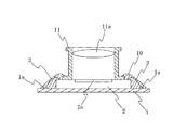
図3は、このように基板上に筐体を実装した従来のカメラモジュールの一例を示す概略断面図である。基板1上には固体撮像素子2が実装されており、複数本のワイヤー3により基板1上に形成された電極1aとの接続がなされている。更に、基板1上には、実装された固体撮像素子2とワイヤー3を覆うようにレンズバレル5を搭載した筐体4が接着剤等により固定され、カメラモジュールとして構成されている。
基板上に筐体を実装する際には、筐体に保持されたレンズの光軸と固体撮像素子面とを垂直にする必要がある。しかしながら、筐体が実装される基板は、通常フレキシブル基板やセラミック基板等であり歪みや撓みが生じやすいため、筐体を基板上に実装する際、筐体が基板に対して傾き、それに伴ってレンズの光軸と固体撮像素子面との間に傾きが生じてしまうことがあった。レンズの光軸と固体撮像素子面との間に傾きが生じたものは、当然ながら良好な画像を得ることはできない。 When mounting the housing on the substrate, it is necessary to make the optical axis of the lens held by the housing and the surface of the solid-state imaging device perpendicular to each other. However, since the substrate on which the housing is mounted is usually a flexible substrate, a ceramic substrate, or the like and is likely to be distorted or bent, when the housing is mounted on the substrate, the housing is inclined with respect to the substrate, and accordingly In some cases, an inclination occurs between the optical axis of the lens and the surface of the solid-state imaging device. Of course, a good image cannot be obtained if there is a tilt between the optical axis of the lens and the surface of the solid-state imaging device.
また、従来の構成では基板に実装された固体撮像素子を覆うように筐体を実装しているため、筐体の外形サイズが大きくなってしまい、カメラモジュールの小型化に歯止めをかけていた。カメラモジュールの小型化は解決すべき重要な課題であるが、前述のように携帯機器の小型化が加速する中で、このような従来の構成では小型化に限界があった。本発明は、このような問題点に鑑みてなされたものであり、固体撮像素子面に対する筐体(レンズ)の傾きを最小限に抑えた小型なカメラモジュールを提供することを目的とする。 Further, in the conventional configuration, since the casing is mounted so as to cover the solid-state imaging device mounted on the substrate, the outer size of the casing is increased, and the downsizing of the camera module is stopped. Although downsizing of the camera module is an important issue to be solved, as described above, miniaturization of portable devices has accelerated, and there has been a limit to downsizing in such a conventional configuration. The present invention has been made in view of such problems, and an object of the present invention is to provide a small camera module in which the inclination of the housing (lens) with respect to the surface of the solid-state imaging device is minimized.
少なくとも、電極が形成された基板と、当該基板に実装された撮像素子と、当該撮像素子の受光領域を覆うように当該撮像素子上に実装された筐体と、で構成されるカメラモジュールとする。 A camera module including at least a substrate on which an electrode is formed, an imaging device mounted on the substrate, and a housing mounted on the imaging device so as to cover a light receiving region of the imaging device. .
前記撮像素子は、導線により前記基板に形成された電極と接続されているカメラモジュールとする。 The imaging element is a camera module connected to an electrode formed on the substrate by a conductive wire.
前記導線、及び前記撮像素子の外周部は、樹脂により覆われているカメラモジュールとする。 The conducting wire and the outer peripheral portion of the imaging device are camera modules covered with resin.
前記撮像素子は前記基板にフリップチップ実装され、且つ前記基板は前記撮像素子の受光領域と対向する位置に開口部を有しており、前記筐体は当該開口部を通して前記撮像素子上に実装されているカメラモジュールとする。 The image sensor is flip-chip mounted on the substrate, and the substrate has an opening at a position facing the light receiving region of the image sensor, and the housing is mounted on the image sensor through the opening. Camera module.
前記筐体の外周面には、前記開口部周縁を遮蔽する鍔部が設けられているカメラモジュールとする。 The camera module is provided with a flange that shields the periphery of the opening on the outer peripheral surface of the casing.
前記筐体外周と前記開口部周縁との間には樹脂が塗布されているカメラモジュールとする。 A camera module in which a resin is applied between the outer periphery of the housing and the periphery of the opening.
前記筐体と前記撮像素子との接触面端部は、樹脂により覆われているカメラモジュールとする。 An end portion of the contact surface between the housing and the image sensor is a camera module covered with resin.
前記樹脂は、遮光性を有するカメラモジュールとする。 The resin is a camera module having a light shielding property.
前記筐体と前記撮像素子とは遮光性の接着剤により接合されているカメラモジュールとする。 The housing and the image sensor are camera modules that are joined by a light-shielding adhesive.
本発明では、レンズを保持した筐体を固体撮像素子上に直接実装しているため、従来のように基板の歪みや撓みによりレンズの光軸と固体撮像素子面との間で角度的なずれがなくなり良好な画像が得られる。また、固体撮像素子やワイヤーを樹脂にて保護するようにしているため、固体撮像素子を覆っていた筐体部分のスペースが不要となり、筐体の外形サイズを小さくすることができる。 In the present invention, since the housing holding the lens is directly mounted on the solid-state image sensor, an angular shift between the optical axis of the lens and the surface of the solid-state image sensor due to distortion or deflection of the substrate as in the past. A good image can be obtained. In addition, since the solid-state imaging device and the wire are protected by the resin, the space of the housing portion that covers the solid-state imaging device is not necessary, and the external size of the housing can be reduced.
基板に固体撮像素子を実装し、固体撮像素子の受光エリア外の部分にレンズ付きの筐体を搭載する。固体撮像素子の電極と基板の電極とはワイヤーにより接続し、ワイヤー全体と固体撮像素子の外部に露出した部分には樹脂を塗布して保護する。 A solid-state image sensor is mounted on a substrate, and a housing with a lens is mounted on a portion outside the light receiving area of the solid-state image sensor. The electrode of the solid-state imaging device and the electrode of the substrate are connected by a wire, and a resin is applied to the whole wire and a portion exposed to the outside of the solid-state imaging device for protection.
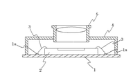
図1は、本発明の一実施例を示す概略断面図である。尚、従来と同部材には同符号を付してある。基板1上には固体撮像素子2が接着剤(不図示)により固定されており、導電性のワイヤー3により基板1上に形成された電極1aとの電気的な導通がなされている。ワイヤー3や固体撮像素子2の外周部は、そのままではショートや破損の恐れがあるため、例えばエポキシ系の樹脂10等を塗布して外部から保護する必要がある。樹脂10は、少なくともワイヤー3と固体撮像素子2の外周部を覆う分だけ塗布されていればよく、従来のような筐体4を用いて覆うのに比べて外形サイズが大きくなることはない。つまり、樹脂10を塗布するスペースの方が筐体4で覆うスペースより小さくて済む。また、基板1としてはセラミック材質のものや、ガラスエポキシ又はフレキシブル基板等が挙げられるが、用途に応じて適宜選択が可能である。
FIG. 1 is a schematic sectional view showing an embodiment of the present invention. In addition, the same code | symbol is attached | subjected to the same member as the past. A solid-state imaging device 2 is fixed on the
固体撮像素子2上には、受光エリア2aを覆うようにレンズ11aが組み込まれた筐体11が実装されている。一般に固体撮像素子2の受光エリア2a外周は、絶縁膜(不図示)で覆われたシリコン部分であり、軽量な部品であれば乗せることのできるスペースが存在する。筐体11は、プラスチック等からなる軽量な部品であり、この受光エリア2a外周のスペースに接着剤(不図示)により固定されている。但し、製造する際には接着剤が固体撮像素子2の受光エリア2aにはみ出さないように注意する必要がある。
On the solid-state imaging device 2, a
一般的に固体撮像素子は、シリコン(Si)から形成されており、その表面は平坦であり、尚且つフレキシブル基板やセラミック基板等と比べて応力に対する歪みや撓みが少ない。そのため、筐体を固体撮像素子上に直接実装すれば、必然的にレンズの光軸と固体撮像素子面との角度的な位置決めが正確になされる。 In general, a solid-state imaging device is made of silicon (Si), and the surface thereof is flat, and there is less distortion and bending with respect to stress compared to a flexible substrate, a ceramic substrate, or the like. Therefore, if the housing is directly mounted on the solid-state image sensor, the optical positioning of the lens and the solid-state image sensor surface are necessarily accurately positioned.
また、ワイヤー3に塗布する樹脂10に遮光性のものを用い、筐体11と固体撮像素子2との接合面端部もいっしょに覆うことにより、筐体11と固体撮像素子2との隙間から筐体11内部にゴミや光が侵入するのを防止することができると共に、筐体11の固体撮像素子2に対する接着強度を高めることができる。筐体11と固体撮像素子2との接着面端部に塗布する樹脂は、ワイヤー3に塗布する樹脂10とは別にして別途塗布するようにしてもよいが、作業性を考えるとワイヤー3に塗布する樹脂10で一度に覆ってしまうのがよい。尚、光の侵入を防止するという意味では、筐体11を固体撮像素子2上に接着する接着剤にも遮光性のものを用いるのが望ましい。
Further, by using a light-
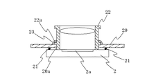
図2は、本発明の別の実施例を示す概略断面図である。前述の実施例1では、固体撮像素子を基板上に実装してワイヤーにより基板との導通を取る形態について説明したが、本実施例2では、固体撮像素子を基板裏面側にフリップチップ実装した形態について説明する。 FIG. 2 is a schematic sectional view showing another embodiment of the present invention. In the above-described first embodiment, the configuration in which the solid-state imaging device is mounted on the substrate and is electrically connected to the substrate by the wire has been described. Will be described.
基板20の裏面側には固体撮像素子2がフリップチップ実装されており、固体撮像素子2の受光エリア2a側の面に形成された電極(不図示)と基板裏面に形成された電極(不図示)とが導電性接着剤21等を介して接続されている。基板20の固体撮像素子2の受光エリア2aと対向する位置には開口部20aが設けられており、そこを通して固体撮像素子2の受光エリア2aが露呈されている。開口部20aは、筐体22の外形寸法に合せて受光エリア2aよりも広く形成されており、その部分を通して筐体22が固体撮像素子2上に実装されている。
The solid-state imaging device 2 is flip-chip mounted on the back surface side of the
また、開口部20aの周縁には遮光性の樹脂23等を塗布して開口部20aと筐体20との隙間を埋めてあり、固体撮像素子2側へゴミや光が侵入するの防止すると共に、筐体22と基板20との接着強度を高めている。特に本実施例では、筐体22の外周面には開口部20aの周縁を遮蔽する鍔部22aを設けてあり、これにより筐体22と開口部20aとの隙間を外部から遮蔽すると共に、樹脂23による固着力を更に高めている。
In addition, a light-
このように、固体撮像素子をフリップチップ方式にて基板に実装することにより、実施例1のようなワイヤーが不要となり、尚且つ筐体が開口部を通して実装されることで基板表面に固体撮像素子を実装する場合に比べて筐体の高さ方向への突出が少なくなるため、より一層の小型化が可能となる。 As described above, by mounting the solid-state imaging device on the substrate by the flip-chip method, the wire as in the first embodiment becomes unnecessary, and the housing is mounted through the opening so that the solid-state imaging device is mounted on the substrate surface. Since the protrusion in the height direction of the housing is reduced as compared with the case of mounting, further miniaturization is possible.
以上説明したように、本発明の要旨は、固体撮像素子上に直接筐体を実装して、筐体の基板に対する実装時の傾きを最小限に抑えると共に、構成の小型化を図ることであり、その技術的範囲は本明細書に記載した実施形態に限定されるものではなく、本発明の趣旨を逸脱しない範囲においてはその他の構成にて実施することも可能である。 As described above, the gist of the present invention is to mount the casing directly on the solid-state imaging device, to minimize the inclination of the casing when mounted on the substrate, and to reduce the size of the configuration. The technical scope is not limited to the embodiments described in the present specification, and other configurations may be implemented without departing from the gist of the present invention.
1 基板
1a 電極
2 固体撮像素子
2a 受光エリア
3 ワイヤー
4 筐体
5 レンズバレル
10 樹脂
11 筐体
11a レンズ
20 基板
20a 開口部
21 導電性接着剤
22 筐体
22a 鍔部
23 樹脂
DESCRIPTION OF
Claims (9)
Priority Applications (1)
| Application Number | Priority Date | Filing Date | Title |
|---|---|---|---|
| JP2004104959A JP2005295050A (en) | 2004-03-31 | 2004-03-31 | Camera module |
Applications Claiming Priority (1)
| Application Number | Priority Date | Filing Date | Title |
|---|---|---|---|
| JP2004104959A JP2005295050A (en) | 2004-03-31 | 2004-03-31 | Camera module |
Publications (1)
| Publication Number | Publication Date |
|---|---|
| JP2005295050A true JP2005295050A (en) | 2005-10-20 |
Family
ID=35327527
Family Applications (1)
| Application Number | Title | Priority Date | Filing Date |
|---|---|---|---|
| JP2004104959A Pending JP2005295050A (en) | 2004-03-31 | 2004-03-31 | Camera module |
Country Status (1)
| Country | Link |
|---|---|
| JP (1) | JP2005295050A (en) |
Cited By (13)
| Publication number | Priority date | Publication date | Assignee | Title |
|---|---|---|---|---|
| WO2008096584A1 (en) * | 2007-02-07 | 2008-08-14 | Konica Minolta Opto, Inc. | Imaging device manufacturing method, imaging device and portable terminal |
| JP2008263552A (en) * | 2007-04-13 | 2008-10-30 | Matsushita Electric Ind Co Ltd | Solid-state imaging device and manufacturing method thereof |
| JP2008263550A (en) * | 2007-04-13 | 2008-10-30 | Matsushita Electric Ind Co Ltd | Solid-state imaging device and manufacturing method thereof |
| JP2008263551A (en) * | 2007-04-13 | 2008-10-30 | Matsushita Electric Ind Co Ltd | Solid-state imaging device and manufacturing method thereof |
| JP2008312104A (en) * | 2007-06-18 | 2008-12-25 | Panasonic Corp | Solid-state imaging device and manufacturing method thereof |
| JP2010510542A (en) * | 2006-11-16 | 2010-04-02 | テッセラ・ノース・アメリカ・インコーポレイテッド | Control of stray light and related method in camera system employing optical laminate |
| JP2011215183A (en) * | 2010-03-31 | 2011-10-27 | Ricoh Co Ltd | Imaging apparatus |
| JP2013020267A (en) * | 2007-04-24 | 2013-01-31 | Digitaloptics Corp | Auto focus/zoom module using wafer level optics |
| WO2013073578A1 (en) * | 2011-11-15 | 2013-05-23 | 株式会社フジクラ | Image capture element chip mounting method, endoscope assembly method, image capture module, and endoscope |
| US8937681B2 (en) | 2007-07-19 | 2015-01-20 | Digitaloptics Corporation | Camera module back-focal length adjustment method and ultra compact components packaging |
| US9118825B2 (en) | 2008-02-22 | 2015-08-25 | Nan Chang O-Film Optoelectronics Technology Ltd. | Attachment of wafer level optics |
| US9419032B2 (en) | 2009-08-14 | 2016-08-16 | Nanchang O-Film Optoelectronics Technology Ltd | Wafer level camera module with molded housing and method of manufacturing |
| US10009528B2 (en) | 2011-02-24 | 2018-06-26 | Nan Chang O-Film Optoelectronics Technology Ltd | Autofocus camera module packaging with circuitry-integrated actuator system |
-
2004
- 2004-03-31 JP JP2004104959A patent/JP2005295050A/en active Pending
Cited By (17)
| Publication number | Priority date | Publication date | Assignee | Title |
|---|---|---|---|---|
| JP2010510542A (en) * | 2006-11-16 | 2010-04-02 | テッセラ・ノース・アメリカ・インコーポレイテッド | Control of stray light and related method in camera system employing optical laminate |
| WO2008096584A1 (en) * | 2007-02-07 | 2008-08-14 | Konica Minolta Opto, Inc. | Imaging device manufacturing method, imaging device and portable terminal |
| JP2008263552A (en) * | 2007-04-13 | 2008-10-30 | Matsushita Electric Ind Co Ltd | Solid-state imaging device and manufacturing method thereof |
| JP2008263550A (en) * | 2007-04-13 | 2008-10-30 | Matsushita Electric Ind Co Ltd | Solid-state imaging device and manufacturing method thereof |
| JP2008263551A (en) * | 2007-04-13 | 2008-10-30 | Matsushita Electric Ind Co Ltd | Solid-state imaging device and manufacturing method thereof |
| JP2013020267A (en) * | 2007-04-24 | 2013-01-31 | Digitaloptics Corp | Auto focus/zoom module using wafer level optics |
| JP2008312104A (en) * | 2007-06-18 | 2008-12-25 | Panasonic Corp | Solid-state imaging device and manufacturing method thereof |
| US8937681B2 (en) | 2007-07-19 | 2015-01-20 | Digitaloptics Corporation | Camera module back-focal length adjustment method and ultra compact components packaging |
| US9118825B2 (en) | 2008-02-22 | 2015-08-25 | Nan Chang O-Film Optoelectronics Technology Ltd. | Attachment of wafer level optics |
| US9419032B2 (en) | 2009-08-14 | 2016-08-16 | Nanchang O-Film Optoelectronics Technology Ltd | Wafer level camera module with molded housing and method of manufacturing |
| JP2011215183A (en) * | 2010-03-31 | 2011-10-27 | Ricoh Co Ltd | Imaging apparatus |
| US9019378B2 (en) | 2010-03-31 | 2015-04-28 | Ricoh Company, Ltd. | Imaging apparatus including a lens barrel holding an optical element |
| US10009528B2 (en) | 2011-02-24 | 2018-06-26 | Nan Chang O-Film Optoelectronics Technology Ltd | Autofocus camera module packaging with circuitry-integrated actuator system |
| WO2013073578A1 (en) * | 2011-11-15 | 2013-05-23 | 株式会社フジクラ | Image capture element chip mounting method, endoscope assembly method, image capture module, and endoscope |
| EP2781183A4 (en) * | 2011-11-15 | 2015-08-12 | Fujikura Ltd | IMAGE CAPTURE ELEMENT CHIP MOUNTING METHOD, ENDOSCOPE ASSEMBLING METHOD, IMAGE CAPTURE MODULE, AND ENDOSCOPE |
| CN103889308A (en) * | 2011-11-15 | 2014-06-25 | 株式会社藤仓 | Image capture element chip mounting method, endoscope assembly method, image capture module, and endoscope |
| US10510918B2 (en) | 2011-11-15 | 2019-12-17 | Fujikura Ltd. | Endoscope imaging module |
Similar Documents
| Publication | Publication Date | Title |
|---|---|---|
| CN100490507C (en) | Small-sized camera shooting component | |
| CN1225111C (en) | small camera module | |
| JP4276678B2 (en) | Imaging device | |
| US20080252771A1 (en) | Camera module with compact packaging of image sensor chip and method of manufacturing the same | |
| US20120268644A9 (en) | Camera module | |
| KR100712449B1 (en) | Image pickup device and camera module | |
| JP2005295050A (en) | Camera module | |
| US20130265470A1 (en) | Camera module for portable device | |
| KR20210031068A (en) | Image sensor package | |
| JP2007208045A (en) | Imaging device, camera module, electronic device, and manufacturing method of imaging device | |
| CN106998414B (en) | Image sensor module and camera module including the same | |
| KR20190019729A (en) | Camera module | |
| WO2007096992A1 (en) | Imaging device and portable terminal device | |
| WO2022135256A1 (en) | Camera module and electronic device | |
| JP4696192B2 (en) | Solid-state image pickup device unit, manufacturing method thereof, and image pickup apparatus | |
| JP2004153855A (en) | Imaging device | |
| JP5093324B2 (en) | Solid-state image pickup device unit, manufacturing method thereof, and image pickup apparatus | |
| KR101038492B1 (en) | Camera module and its manufacturing method | |
| US11991429B2 (en) | Camera module | |
| JP2010220245A (en) | Imaging device, camera module, electronic device, and method of manufacturing imaging device | |
| JP4424470B2 (en) | Solid-state imaging device | |
| JP4806970B2 (en) | Solid-state imaging device | |
| KR101055569B1 (en) | Camera module | |
| JP2006135577A (en) | Solid-state imaging apparatus and electronic equipment provided with same | |
| KR101026830B1 (en) | Camera module |