EP2780693B1 - Mikrostrukturierte chip mit konvexen oberflächen für oberflächenplasmonresonanzanalyse, analysevorrichtung mit diesem mikrostrukturierten chip und verwendung der vorrichtung - Google Patents
Mikrostrukturierte chip mit konvexen oberflächen für oberflächenplasmonresonanzanalyse, analysevorrichtung mit diesem mikrostrukturierten chip und verwendung der vorrichtung Download PDFInfo
- Publication number
- EP2780693B1 EP2780693B1 EP12794369.4A EP12794369A EP2780693B1 EP 2780693 B1 EP2780693 B1 EP 2780693B1 EP 12794369 A EP12794369 A EP 12794369A EP 2780693 B1 EP2780693 B1 EP 2780693B1
- Authority
- EP
- European Patent Office
- Prior art keywords
- chip
- cavities
- protuberances
- microstructured chip
- face
- Prior art date
- Legal status (The legal status is an assumption and is not a legal conclusion. Google has not performed a legal analysis and makes no representation as to the accuracy of the status listed.)
- Active
Links
Images



Classifications
-
- G—PHYSICS
- G01—MEASURING; TESTING
- G01N—INVESTIGATING OR ANALYSING MATERIALS BY DETERMINING THEIR CHEMICAL OR PHYSICAL PROPERTIES
- G01N21/00—Investigating or analysing materials by the use of optical means, i.e. using sub-millimetre waves, infrared, visible or ultraviolet light
- G01N21/17—Systems in which incident light is modified in accordance with the properties of the material investigated
- G01N21/55—Specular reflectivity
-
- C—CHEMISTRY; METALLURGY
- C12—BIOCHEMISTRY; BEER; SPIRITS; WINE; VINEGAR; MICROBIOLOGY; ENZYMOLOGY; MUTATION OR GENETIC ENGINEERING
- C12Q—MEASURING OR TESTING PROCESSES INVOLVING ENZYMES, NUCLEIC ACIDS OR MICROORGANISMS; COMPOSITIONS OR TEST PAPERS THEREFOR; PROCESSES OF PREPARING SUCH COMPOSITIONS; CONDITION-RESPONSIVE CONTROL IN MICROBIOLOGICAL OR ENZYMOLOGICAL PROCESSES
- C12Q1/00—Measuring or testing processes involving enzymes, nucleic acids or microorganisms; Compositions therefor; Processes of preparing such compositions
- C12Q1/68—Measuring or testing processes involving enzymes, nucleic acids or microorganisms; Compositions therefor; Processes of preparing such compositions involving nucleic acids
- C12Q1/6813—Hybridisation assays
- C12Q1/6816—Hybridisation assays characterised by the detection means
-
- G—PHYSICS
- G01—MEASURING; TESTING
- G01N—INVESTIGATING OR ANALYSING MATERIALS BY DETERMINING THEIR CHEMICAL OR PHYSICAL PROPERTIES
- G01N21/00—Investigating or analysing materials by the use of optical means, i.e. using sub-millimetre waves, infrared, visible or ultraviolet light
- G01N21/17—Systems in which incident light is modified in accordance with the properties of the material investigated
- G01N21/55—Specular reflectivity
- G01N21/552—Attenuated total reflection
- G01N21/553—Attenuated total reflection and using surface plasmons
-
- G—PHYSICS
- G01—MEASURING; TESTING
- G01N—INVESTIGATING OR ANALYSING MATERIALS BY DETERMINING THEIR CHEMICAL OR PHYSICAL PROPERTIES
- G01N21/00—Investigating or analysing materials by the use of optical means, i.e. using sub-millimetre waves, infrared, visible or ultraviolet light
- G01N21/17—Systems in which incident light is modified in accordance with the properties of the material investigated
- G01N21/25—Colour; Spectral properties, i.e. comparison of effect of material on the light at two or more different wavelengths or wavelength bands
- G01N21/251—Colorimeters; Construction thereof
- G01N21/253—Colorimeters; Construction thereof for batch operation, i.e. multisample apparatus
Definitions
- the present invention relates to a microstructured chip comprising convex surfaces for Resonance analysis of Surface Plasmons, an analysis device comprising said microstructured chip, a method of analysis and the uses of said device.
- SPR Surface Plasmon Resonance
- SPR Surface Plasmon Resonance
- This technique is best known for making it possible to follow in real time, and without a marker (of the fluorescent or radioactive type for example), biomolecular interactions. It makes it possible in particular to qualify and quantify interactions between ligands immobilized on a surface and analytes in solution in a sample.
- SPR is a physical phenomenon of collective excitation of the electrons of a metal on a metal-dielectric medium interface (said dielectric medium typically being a liquid medium or a gas).
- dielectric medium typically being a liquid medium or a gas.
- TM Magnetic Transverse polarization
- plasmon resonance angle a phenomenon occurs resonance resulting in the coupling of the incident light energy to a surface wave (called “surface plasmon”) propagating parallel to the interface.
- surface plasmon surface wave
- incident radiation arrives at a given angle of incidence on one of the lateral faces of a chip (generally a prism in the state of the art, since it is the method of coupling light on the sensitive surface most simple to use) one of the faces of which is covered with a metallic layer, said incident radiation is refracted when it enters the prism (due to the difference in optical index between the medium constituting the prism and the previous optical medium, generally air) and is reflected on said metal surface.
- This configuration is well known to those skilled in the art under the name of Kretschmann configuration ( E. Kretschmann, The determination of the Optical Constants of Metals by Excitation of Surface Plasmons, Z Physik 241: 313-324 (1971 )).
- the phenomenon of SPR can also make it possible to study biomolecular interactions.
- ligands are immobilized beforehand on the metallic surface of the prism in defined zones.
- any subsequent attachment of other molecules with these ligands will locally modify the optical thickness at the level of said defined zones, and will therefore cause variations in the resonance conditions and therefore a displacement of the resonance angle.
- This displacement is, as a first approximation, proportional to the quantity of biological material which has come to interact with the ligands.
- small molecules will cause a small displacement of the angle of incidence while larger molecules will induce a much greater angular offset.
- It is the study of variations in optical reflectivity linked to the resonance phenomenon which will make it possible to detect and measure biomolecular interactions and their temporal evolution in defined areas.
- SPR devices making it possible to carry out imaging and to follow, at fixed angle of incidence and wavelength, the evolution of the biomolecular interactions in zones defined on a chip.
- the documents US 7678584 (Guédon et al ), US 7576863 (Weibel and al ), US 7,551,286 (Tani et al ) have such SPR devices. Although these devices allow an analysis of several interactions in parallel, they present moving parts or do not allow a detailed analysis of the interaction when no part is moving.
- the useful detection surface is a flat metallized surface, and only allows an analysis to be made at a precise angle angle.
- an SPR analysis device comprising a microstructured chip having a particular architecture made it possible to meet these requirements.
- chip or “microstructured chip” will be used interchangeably in the remainder of the text.
- m is different from 0 (m> 0).
- the upper face of the chip is provided with micrometric size zones intended to receive species to be analyzed chosen from at least one protuberance and at least one cavity.
- microstructured chip is meant a chip having zones of micrometric size intended to receive species to be analyzed.
- the chip is not necessarily of micrometric size but includes areas which are of micrometric size.
- micrometric size zones zones which have at least two dimensions out of three of micrometric size, said micrometric dimensions ranging from 1 ⁇ m to 1000 ⁇ m, and preferably from 10 ⁇ m to 500 ⁇ m.
- the third dimension of the zone is therefore not necessarily micrometric and may have distances between 1mm and 20mm, preferably between 1mm and 10mm.
- the zones according to the invention have particular geometries in the form of protuberances and possibly cavities which will be described later. It is in these areas covered with a metallic layer that the plasmon effect will be observed.
- At least part of the upper face is coated with the metal layer. It represents the useful detection surface (also called sensitive surface below).
- at least one zone of micrometric size chosen from n protrusions and m cavities is coated with the metallic layer.
- the upper face is entirely covered by the metal layer.
- not only the zones but also the flat surfaces separating said zones are intended to receive species to be analyzed.
- the direct orthonormal reference frame (XYZ) is used in which the plane surfaces separating the zones are parallel to the plane (XY) and in which the Z axis is oriented downwards.
- flat surfaces flat or substantially flat surfaces which may have some defects.
- the zones are arranged in the form of a matrix on the upper face of the chip.
- the flat surfaces separate the zones both along the X axis and the Y axis.
- the zones are arranged in the form of continuous chutes along the upper face of the chip.
- the flat surfaces separate the zones along the X axis or along the Y axis.
- the zones are separated by a distance D along the Y axis and by a distance D 'along the X axis by the plane surfaces (or inter-zone surfaces); D and D'being between 0 ⁇ m (in the case of a continuous chute along one of the X or Y axes) and 5mm, preferably between 50pm and 5mm, preferably between 200 and 1000 ⁇ m and particularly preferably between 300 and 700pm.
- the zones are separated by a center to center distance CTC of between 10 pm and 25000 pm, preferably between 50 pm and 5000 pm and more preferably between 100 ⁇ m and 1000 ⁇ m.
- planar surfaces belong to planes parallel to the plane (XY); the face superior is then presented in the form of stair treads.
- the plane surfaces belong to the same plane (XY) (that is to say Z is constant).
- protuberance is meant a protuberance on the upper face of the chip, said protuberance being located between two flat surfaces (also called inter-zone surface).
- the protuberance can be defined either in 3 dimensions (reference XYZ) or in 2 dimensions (section in a plane).
- a protuberance is called a volume of which all the coordinates are above a fictitious plane connecting the two plane inter-zone surfaces adjacent to said protuberance.
- a protuberance according to the invention is defined by at least one curve of mean radius of curvature R and / or at least one straight line.
- the curve is necessarily convex (that is to say radius of curvature along the axis + Z).
- the curve can be either concave (that is to say radius of curvature along the axis - Z), or convex.
- the protuberance is defined by two straight lines separated by a curve.
- the two lines are parallel.
- the two straight lines have different dimensions.
- ⁇ is meant a hollow in the upper face of the chip, the said hollow being located between two flat surfaces (also called inter-zone surface).
- the cavity can be defined either in 3 dimensions (reference XYZ) or in 2 dimensions (section in a plane).
- a cavity is called a volume of which all the coordinates are under a fictitious plane connecting the two plane inter-zone surfaces adjacent to said cavity.
- a cavity according to the invention is described in the plane (YZ) and is defined by at least one curve of mean radius of curvature R and / or at least one straight line.
- the curve is necessarily concave (that is to say radius of curvature along the axis -Z).
- the curve can be either concave or convex (that is to say radius of curvature along the axis + Z).
- the cavity is defined by two straight lines separated by a curve.
- the two lines are parallel.
- the two straight lines have different dimensions.
- the areas of the chip are defined by a curve with an average radius of curvature R (concave for a cavity and convex for a protuberance); the radius of curvature R being between 0.1mm and 600mm, preferably between 0.3mm and 300mm.
- R average radius of curvature
- n protrusions and m cavities of semi-spherical, semi-elliptical or semi-cylindrical shape (reference (XYZ)).
- the n protrusions and m cavities have a semi-cylindrical shape in the coordinate system (XYZ).
- the radius of curvature of the zones i.e. n protrusions and m cavities
- the plane (XY) that is to say along the axis Z.
- the base of the chip can be a flat or curved surface, or an edge, or a point.
- the base of the chip is a flat surface which, preferably, is parallel to the flat surfaces (also called inter-zone surfaces).
- the plane surfaces belong to the same plane (XY).
- XY the distances between the flat surfaces and the base of the chip are identical.
- the planar surfaces belong to multiple planes parallel to the plane (XY).
- the distances between the surfaces planes and the base of the chip are different (upper face in the shape of a staircase).
- distances between the plane surfaces (or inter-zone surfaces) and the base it is referred to the heights of the chip, that is to say to the length of the perpendicular connecting the surfaces and the base or a base extension.
- the side (s) side (s) of the chip can (can) be plane (s) or perpendicular (s) to the base and / or to the upper face of the chip ) or curve (s).
- the side (s) side (s) of the chip is (are) plane (s).
- At least one lateral face of the chip is perpendicular to the base and / or to the upper face.
- the upper face is parallel to the base of the chip.
- the chip is attached to a prism well known in the state of the art.
- the chip is in the form of a parallelepiped (that is to say a chip having plane surfaces belonging to the same plane (XY) and a base parallel to said plane surfaces ).
- the heights of the lateral surfaces are of small dimensions of the order of 0.1mm to 20mm, preferably from 1mm to 10mm).
- species to be analyzed is meant, for example, materials, gases or biological species such as single or double-stranded DNA, proteins, bacteria, toxins, viruses, mycoplasmas, chemical agents or any other biological or chemical species likely to interact with other biological or chemical species.
- the species to be analyzed are biological species, such as pathogenic bacteria such as Salmonella spp., Listeria monocytogenes, Clostridium difficile, or even Campylobacter spp.
- pathogenic bacteria such as Salmonella spp., Listeria monocytogenes, Clostridium difficile, or even Campylobacter spp.
- the present inventor has demonstrated that it is possible, using the chip according to the invention, to advantageously study strains of Escherichia coli producing shigatoxins (STEC), because it allows the simultaneous analysis of large molecules (bacteria themselves ), but also the small toxins they produce.
- STC Escherichia coli producing shigatoxins
- the n protrusions and m cavities will be functionalized with different monoclonal antibodies specific for biomarkers.
- the figure 3 represents a microstructured chip 3 in which the upper face 4 comprising plane inter-protuberance surfaces is parallel to the base 5 of the chip 3.
- the upper face 4 is covered with a metallic layer 2 and is provided with protrusions 1 sensitive to the 'plasmon effect, intended to receive species to be analyzed.
- the protrusions 1 are separated from each other by a distance D along the axis Y and by a distance D 'along the axis X by plane surfaces (also called inter-protuberance surfaces).
- the microstructured chip 3 can be made of any type of material allowing the propagation of light. Mention may be made, for example, of glass, a crystal or plastics.
- the chip 3 is made of plastic material (s) such as for example PMMA (polymethyl methacrylate), PC (Polycarbonate), PS (Polystyrene), SU-8 (negative epoxy-based photosensitive resin) or PDMS (Polydimethylsiloxane).
- plastic material such as for example PMMA (polymethyl methacrylate), PC (Polycarbonate), PS (Polystyrene), SU-8 (negative epoxy-based photosensitive resin) or PDMS (Polydimethylsiloxane).
- the chip when attached to a prism, it can be made of a material different from that of the prism.
- the metal layer 2 which covers the upper layer 4 of the chip 3 (and in particular the protrusions 1) can be produced with various metals such as gold, silver, platinum or aluminum.
- the metal layer 2 is made of gold.
- the thickness of the metal layer 2 is between 10 nm and 200 nm, preferably between 30 nm and 100 nm and even more preferably between 40 nm and 50 nm.
- a thin layer of chromium is used as the pre-bonding layer of the gold on the upper face 4 of the chip 3.
- the figure 4 represents the upper face of a microstructured chip according to the invention entirely covered with a metallic layer 2, said microstructured chip is provided with protuberances which are arranged in the form of chutes along the axis X thus forming 4 columns C 1 - C 4 .
- d represents the diameter of the chute and CTC represents the center to center distance between two successive chutes.
- the chip according to the invention makes it possible to adapt the sensitivity of each zone (that is to say n protrusions and m cavities) in order to study very different biological species.
- At least one of the n protrusions and m cavities has a radius of curvature different from the others.
- the figure 5 represents a sectional enlargement of the figure 3 the convex curved surface protrusion 1 of the chip 3 (covered with the metal layer 2) which is irradiated by a collimated monochromatic beam of angle of incidence ⁇ and linearly polarized according to the polarization TM.
- the protrusion, semi-cylindrical in shape (in the XYZ coordinate system), having a surface defined by a single curve (in the ZY plane) on the figures 3 and 5 , is characterized by its radius of curvature R and by the two half-angles ⁇ (thus defining a total angle of 2 ⁇ ).
- the radius of curvature R and the half-angle ⁇ will thus define the length of the cord d, or even the diameter of said cavity.
- the choice of the radius of curvature R of the n protrusions and m cavities of the chip according to the invention is very important because it will determine, as a function of the essential physical parameters (index optic of the chip n P , optical index of the external dielectric medium n e , average angle of incidence of the collimated beam ⁇ and the size of the biological species which it is desired to analyze), the sensitivity and the angular dynamics of the measurement, for each of the n protrusions and m cavities.
- angular dynamics of the measurement is meant the angular range which will be able to be displayed during the analyzes.
- sensitivity we mean the smallest variation in optical thickness that we will be able to measure on the sensitive surface.
- At least one of the n protrusions and m cavities has a tilt (or tilting) of an angle ⁇ .
- the radius of curvature R is deviated with respect to the axis Z.
- the figure 6 represents an enlargement in section of a protuberance of a convex curved surface 41 of a chip 43 (the upper face of which is covered with a metal layer 42) which has a tilt of an angle ⁇ and which is irradiated by a monochromatic beam collimated with an average angle of incidence ⁇ and linearly polarized in the transverse magnetic direction TM.
- the angle ⁇ is defined as follows: 0 ° ⁇ 80 °, preferably 15 ° ⁇ ⁇ 45 °.
- At least one of the zones (that is to say at least one of the n protrusions and of the m cavities) has both a different radius of curvature and a different orientation with respect to the other zones of the chip.
- At least one distance between the base and the flat surfaces is different from the others.
- the figure 7 shows a chip 33 whose upper face 44 which is covered with a metal layer 22 is provided with protrusions of curved shape 11.
- the lateral faces (55, 66) of the chip 33 are perpendicular to the base 77 and to the flat surfaces.
- the distances between the flat surfaces between the protrusions 11 (or inter-protuberance surfaces) and the base 77 are all different from each other with d4 ⁇ d3 ⁇ d2 ⁇ d1.
- the inter-zone surfaces belong to multiple planes parallel to the plane (XY) (5 planes shown).
- the chip according to the invention can be produced by different methods which necessarily include a step of manufacturing the chip followed by a step of depositing at least one thin metallic layer.
- the chip is manufactured by high pressure injection.
- the production of the chip according to the invention requires the use of a mold of concave shape in order to produce a protuberance of convex shape, which thus makes it possible to reduce its production cost.
- a person skilled in the art knows that the most costly step during the development of a production of components by the high pressure injection process is the production of the mold (or "master").
- the fact of having a final surface of the part to be produced with convex protrusions will make it possible to produce a mold with concave shapes, which amounts to removing material in the "master", which is very simple to produce with conventional mechanical machining methods.
- Cold deposition techniques are useful in particular in the case of a plastic support since the plastic does not support significant temperature increases.
- the figures 8 and 9 represent different embodiments of measurement devices comprising the microstructured chip described above.
- the coupling between the energy of the incident beam and the surface wave of the metal surface of the chip is carried out by the chip itself.
- the coupling means is a prism, a waveguide or a diffraction grating.
- the chip according to the invention when the coupling is carried out by a prism, the chip according to the invention is attached to said prism so that the base of the chip is brought into contact with the upper face of the prism not having metal surface using an index coupling oil which is a method well known to those skilled in the art.
- the chip is attached to a waveguide.
- the chip is attached to a diffraction grating.
- the source 7 can be, for example, a mercury vapor lamp, an incandescent lamp, a laser diode, a laser, a light-emitting diode (LED) or an organic light-emitting diode (OLED).
- a mercury vapor lamp an incandescent lamp
- a laser diode a laser
- a light-emitting diode LED
- OLED organic light-emitting diode
- the source 7 is a monochromatic LED.
- monochromatic we mean an LED whose spectral width at half height does not exceed 40nm.
- wavelength ranges can be used such as the visible or the near infrared (IR).
- a wavelength between 790 and 825nm is used.
- the beam can be collimated.
- various techniques well known to those skilled in the art may be used.
- a collimating optical system 8 a first converging lens which makes it possible to focus the light emitted by the source 7 on a hole of diameter ⁇ , said hole being in the focal plane of a converging lens ce which generates the collimated beam.
- the optical collimation system 8 is integrated into the source 7.
- the polarizing system 6 makes it possible to work in Magnetic Transverse mode (or TM, or p-polarization).
- linear polarizer or a polarizing separator cube.
- the polarizing system 6 makes it easy to switch from one TM polarization to TE (Electric Transverse) polarization, and vice versa. In order to avoid any movement of the workpiece, this can be done using a liquid crystal blade, controlled by electric currents and voltages.
- the detector (10; 70) can for example be a CCD, CMOS camera or be a matrix of photodetectors.
- the cameras operate on 8, 10, 12 or 16 bits and preferably on 10 or 12 bits.
- the device further comprises an optical imaging system (9; 69) which makes it possible to produce the image of the microstructured chip (3; 33; 43; 53; 63) on the detector (10; 70).
- the optical imaging system (9; 69) must be sufficiently open to accept all the radiation from the microstructured chip.
- the convex geometry of the n protrusions with which the chip according to the invention is endowed makes it possible in particular to make the beams converge after reflection of the incident radiation thereon, thus making the optical imaging system (9; 69) much easier to produce.
- optical imaging system (9; 69) is chosen so that the image of 2 protrusions or 1 protuberance and 1 cavity of the microstructured chip correspond to 2 different positions on the detector (10; 70).
- the optical system has a magnification which maximizes the number of useful pixels on the detector (10; 70).
- optical imaging system (9; 69)
- 2 plano-convex lenses mounted in afocal By way of example as an optical imaging system (9; 69), mention may be made of 2 plano-convex lenses mounted in afocal.
- the face through which an incident radiation enters the chip is called the entry face and the exit face the face through which the radiation reflected by the sensitive surface exits.
- the source 7 emits incident radiation, which is collimated using the collimation system 8 and polarized using the polarizer 6 before arriving at the input face 54 of the chip 53 (covered with a metal layer 52) at a given incidence.
- the radiation is deflected when it enters the chip 53 and is reflected on the protrusions 51.
- the imaging system 9 located after the exit face 57 of said chip 53, makes it possible to collect the intensity of the reflected radiation and to produce the image of the irradiated protuberances 51 on the detector 10.
- the device shown in the figure 9 comprises a chip 61 (covered with a metal layer 62) whose lateral faces are perpendicular to the base and whose distances between the surfaces separating the protrusions 61 from the base are different from each other.
- the figure 9 shows an embodiment in which the incident radiation emitted by the source (not shown in the figure 9 ) which arrives perpendicularly on the input face 64 (corresponding to the lateral face), is not deflected when it crosses the chip 63, and irradiates all of the different protuberances 61.
- the imaging system 69 and the detector 70 are located after the exit face 67, which in this embodiment corresponds to the base of said chip 63, thus making it possible to collect the intensity of the reflected radiation and to produce the image. protrusions 61.
- the optical imaging system (9; 69) can be integrated directly into the exit face (57; 67) of the chip (53; 63) in the form of an array of microlenses.
- the collimation system 8 and possibly the polarizer 6 are made integral with the input face (54; 64) and / or the optical imaging system (9; 69) and the detector (10 ; 70) are made integral with the outlet face (57; 67).
- the immobilization of the ligands on the upper surface can be carried out with various techniques well known to those skilled in the art such as, for example, immobilization by covalent chemical bonding or by electro-copolymerization of pyrrole on the surface. metallic.
- fluid is meant a gas or a liquid.
- the fluid comprises at least one biological species.
- These measurement methods are suitable for measuring, without limitation, variations in the conformation of molecules immobilized on a surface, biomolecular interactions, optical indices of fluids (gas or liquids), the quality of a surface (parallelism, roughness microscopic, quality of a deposit of thin layers) or the presence of metallic nanobeads near the surface.
- the incident beam enters perpendicularly through the input face 64 of the chip 63.
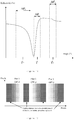
- the 3 angular ranges studied are centered on the angle ⁇ .
- the width of each of the zones is defined by the angle at the apex 2 ⁇ and the radius of curvature R of each of the protuberances or protuberances and cavities.
- the choice of the angle ⁇ is therefore essential to best observe all the areas of interest. It is thus possible, depending on the radius of curvature of the studied area, to explore a more or less large angular range of the plasmon curve. In the case where the zones do not have a tilt ⁇ (this is the case for the figure 10 ) this angular range will always be centered on the same value ⁇ .
- the measurement method further comprises a step in which an image of the n protrusions and of the m cavities of the chip is produced.
- This choice can be made for each of the n protrusions and m cavities, which makes it possible to adapt to several types of species immobilized on the same chip.
- the choice can be made as a function of the type of species which will interact with the species previously immobilized on the chip: it is thus possible to "adapt" each of the protuberances or protuberances and cavities to the species sought.
- Another object of the invention therefore relates to the use of the device according to the invention for the measurement of biomolecular interactions.
- Example 1 Protein chip - monitoring and correction of the index of the external environment in real time in interaction kinetics
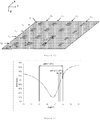
- a microstructured chip made of polycarbonate (PC) comprising 16 protrusions is shown in the figure 13 .
- a layer of gold with a thickness of 48 nm was deposited by sputtering on the upper face of said chip in order to obtain a plasmon effect.
- CTC center-to-center distance
- the chip is irradiated with polarized, collimated and monochromatic incident radiation and the intensity of the radiation reflected by the protuberances is detected by a CMOS type detector.
- the radius of curvature of the semi-cylindrical surfaces of the protrusions of columns C 1 , C 2 and C 3 is 9.5 mm (equivalent to an angular area of study ⁇ a on the plasmon curve of approximately 3 °) and the protrusions of column C 4 have a radius of curvature of 1.9 mm (equivalent to an angular study area ⁇ b of approximately 15 °).
- the angular ranges ⁇ a and ⁇ b correspond respectively to the angular ranges ⁇ 1 and ⁇ 3 on the figure 10 .
- a liquid of unknown optical index containing hCG proteins is contacted with the chip in the protrusions.
- a characteristic variation of the signal is observed as a function of time on the protuberances of the L 2 line but not on the others because a specific interaction takes place on the anti-hCG monoclonal antibodies and not on the other immobilized proteins.
- the protuberance located in (L 2 , C 4 ) has a radius of curvature such that the entire plasmon curve can be viewed on the detector, the angular value of the limit refractive angle can be easily determined and it is thus possible to deduce the index of the unknown liquid medium.
- bacteria in this category are strains O157: H7, O26: H11 or O103: H2.
- Bacteria of this type and the shigatoxins they produce are at the origin of severe intestinal disorders, for which the vital prognosis can be committed.
- the size and molecular weight of these shigatoxins (a few nanometers in diameter and a molecular weight of around 68kDa) is very different from that of an Escherichia coli bacterium (around 10 million times heavier). Consequently, the plasmon signals for the attachment of these 2 types of families are very different.
- conventional SPR devices we cannot therefore study both these bacteria and these toxins in the same experiment and in real time. Indeed, in the case of attachment of bacteria, the curve will shift angularly by nearly 0.1 ° while it will only move less than 0.01 ° in the case of toxins (which does not is not easily detectable by conventional SPR methods).
- the upper face of said chip is covered by a layer of chromium with a thickness of 2 nm and a layer of gold with a thickness of 48 nm both deposited by cathode sputtering in order to obtain a plasmon effect.
- the chip is irradiated with polarized, collimated and monochromatic incident radiation and the intensity of the radiation reflected by the sensitive surface of the protrusions is detected by a CCD type detector.
- the average angle of incidence of the optical system is fixed mechanically by the architecture of the system and is equal to 26.5 °.
- the radius of curvature of the two protrusions is also different: 11.5mm for the first protrusion (corresponding to an angular range of study ⁇ of 3 °) and 100mm for the second (which corresponds to an angular range of analysis ⁇ ' 0.3 °) ( figure 14 ).
- Monoclonal antibodies directed against the bacteria O157: H7 are immobilized covalently and uniformly on the first protuberance and monoclonal antibodies directed specifically against the shigatoxins that the bacteria secretes are immobilized on the second protuberance.
- the two plasmon curves generated from these 2 protuberances have the same plasmon resonance angle (approximately 26.7 °), before reaction.
- ⁇ 0.5 °
- ⁇ ' 0.3 °
- the Figures 15 and 16 represent the signals obtained on the detector for the two protuberances before and after interaction of the antibodies immobilized on each of the protuberances with bacteria and toxins respectively.
- this example demonstrates that the chip according to the invention makes it possible to adapt the dynamics and the sensitivity of measurement to the species to be measured during a single experiment.
Landscapes
- Chemical & Material Sciences (AREA)
- Life Sciences & Earth Sciences (AREA)
- Health & Medical Sciences (AREA)
- Organic Chemistry (AREA)
- Immunology (AREA)
- General Health & Medical Sciences (AREA)
- Analytical Chemistry (AREA)
- Biochemistry (AREA)
- Physics & Mathematics (AREA)
- Zoology (AREA)
- Engineering & Computer Science (AREA)
- Wood Science & Technology (AREA)
- Proteomics, Peptides & Aminoacids (AREA)
- Pathology (AREA)
- General Physics & Mathematics (AREA)
- Bioinformatics & Cheminformatics (AREA)
- Microbiology (AREA)
- General Engineering & Computer Science (AREA)
- Biophysics (AREA)
- Genetics & Genomics (AREA)
- Biotechnology (AREA)
- Molecular Biology (AREA)
- Investigating Or Analysing Materials By Optical Means (AREA)
- Investigating, Analyzing Materials By Fluorescence Or Luminescence (AREA)
Claims (18)
- Mikrostrukturierter Chip (3; 33; 43; 53; 63) zur Oberflächenplasmonresonanzanalyse (SPR-Analyse), welcher in der Form eines Festkörpers vorliegt, der aus einer Grundfläche (5; 77), einer Oberseite (4; 44), von der wenigstens ein Teil mit einer metallischen Schicht (2; 22; 42; 52; 62) bedeckt ist, und wenigstens einer Seitenfläche (55; 66) besteht, wobei:- die Oberseite mit Bereichen (1; 11; 41; 51; 61) mit einer Größe von 1 µm bis 1000 µm ausgestattet ist, die dazu bestimmt sind, zu analysierende Spezies aufzunehmen, die aus n Erhebungen und m Vertiefungen ausgewählt sind; und- wenn n+m ≥ 2 ist, die Bereiche durch ebene Flächen voneinander getrennt sind, wobei die ebenen Flächen parallel zu einer Ebene (XY) sind, mit n von 1 bis j, m von 0 bis i; wobei j und i ganze Zahlen sind;- die Bereiche (1; 11; 41; 51; 61) eine gekrümmte Oberfläche mit einem mittleren Krümmungsradius R aufweisen, der sich in einer zur Ebene (XY) orthogonalen Ebene befindet; und- der mittlere Krümmungsradius R der gekrümmten Oberfläche zwischen 0,1 und 600 mm liegt,dadurch gekennzeichnet, dass wenigstens eine der n Erhebungen und m Vertiefungen (1; 11; 41; 51; 61) einen Krümmungsradius aufweist, der von den anderen verschieden ist.
- Mikrostrukturierter Chip (3; 33; 43; 53; 63) nach Anspruch 1, dadurch gekennzeichnet, dass wenigstens ein aus den n Erhebungen und m Vertiefungen ausgewählter Bereich von der metallischen Schicht bedeckt ist.
- Mikrostrukturierter Chip (3; 33; 43; 53; 63) nach Anspruch 1 oder 2, dadurch gekennzeichnet, dass m = 0 ist.
- Mikrostrukturierter Chip (3; 33; 43; 53; 63) nach Anspruch 1 oder 2, dadurch gekennzeichnet, dass m > 0 ist.
- Mikrostrukturierter Chip (3; 33; 43; 53; 63) nach einem der Ansprüche 1 bis 4, dadurch gekennzeichnet, dass die Grundfläche (5; 77) eine ebene Fläche ist.
- Mikrostrukturierter Chip (3; 33; 43; 53; 63) nach einem der Ansprüche 1 bis 5, dadurch gekennzeichnet, dass die Oberseite (4; 44) parallel zur Grundfläche (5; 77) ist.
- Mikrostrukturierter Chip (3; 33; 43; 53; 63) nach einem der Ansprüche 1 bis 5, dadurch gekennzeichnet, dass wenigstens eine Seitenfläche (55; 66) eben ist.
- Mikrostrukturierter Chip (3; 33; 43; 53; 63) nach Anspruch 6, dadurch gekennzeichnet, dass wenigstens eine Seitenfläche (55; 66) eben ist.
- Mikrostrukturierter Chip (3; 33; 43; 53; 63) nach Anspruch 7, dadurch gekennzeichnet, dass wenigstens eine Seitenfläche (55; 66) senkrecht zur Grundfläche (5; 77) oder zur Oberseite (4; 44) ist.
- Mikrostrukturierter Chip (3; 33; 43; 53; 63) nach Anspruch 8, dadurch gekennzeichnet, dass wenigstens eine Seitenfläche (55; 66) senkrecht zur Grundfläche (5; 77) und zur Oberseite (4; 44) ist.
- Mikrostrukturierter Chip (3; 33; 43; 53; 63) nach einem der Ansprüche 1 bis 10, dadurch gekennzeichnet, dass wenigstens eine der n Erhebungen und m Vertiefungen (1; 11; 41; 51; 61) eine Schwenkung um einen Winkel β aufweist, vorzugsweise derart, dass 0° < β ≤ 80° ist.
- Mikrostrukturierter Chip (3; 33; 43; 53; 63) nach einem der Ansprüche 1 bis 11, dadurch gekennzeichnet, dass wenigstens einer der Abstände, der die ebenen Flächen zwischen den n Erhebungen und m Vertiefungen (1; 11; 41; 51; 61) von der Grundfläche (5; 77) trennt, von den anderen verschieden ist.
- Vorrichtung zur SPR-Analyse, welche umfasst:- eine Lichtquelle (7), die dazu bestimmt ist, einen einfallenden Strahl zu erzeugen;- eventuell ein optisches Kollimationssystem (8);- ein Polarisationssystem (6);- einen mikrostrukturierten Chip (3; 33; 43; 53; 63), wie in einem der Ansprüche 1 bis 12 definiert, der im Strahlengang des einfallenden Strahls angeordnet ist;- eventuell ein optisches Bildgebungssystem (9; 69) ;- einen Detektor (10; 70).
- Vorrichtung nach Anspruch 13, dadurch gekennzeichnet, dass das Kollimationssystem (8) und eventuell der Polarisator (6) mit der Eintrittsseite (54; 64) fest verbunden sind und/oder das optische Bildgebungssystem (9; 69) und der Detektor (10; 70) mit der Austrittsseite (57; 67) fest verbunden sind.
- SPR-Messverfahren, welches die folgenden Schritte umfasst:- Erfassen eines Anfangszustands (i) durch Bestrahlen der empfindlichen Oberfläche wenigstens einer der n Erhebungen und m Vertiefungen über die Eintrittsseite des mikrostrukturierten Chips, wie er in einem der Ansprüche 1 bis 12 definiert ist, mithilfe eines einfallenden monochromatischen Strahls, der zuvor polarisiert und eventuell kollimiert wurde, und (ii) durch gleichzeitiges Erfassen der Intensität der von der empfindlichen Oberfläche wenigstens einer der n Erhebungen und m Vertiefungen reflektierten Strahlungen, die über die Austrittsseite austreten;- Inkontaktbringen wenigstens eines Fluids mit der empfindlichen Oberfläche wenigstens einer der n Erhebungen und m Vertiefungen;- Bestrahlen der empfindlichen Oberfläche wenigstens einer der n Erhebungen und m Vertiefungen, die das Fluid enthalten, über die Eintrittsseite des mikrostrukturierten Chips mithilfe eines einfallenden monochromatischen Strahls, der zuvor polarisiert und eventuell kollimiert wurde, und gleichzeitiges Erfassen der Intensität der von der empfindlichen Oberfläche wenigstens einer der n Erhebungen und m Vertiefungen reflektierten Strahlungen, die über die Austrittsseite austreten, um in Echtzeit und kontinuierlich Änderungen der optischen Dicke in wenigstens einer der n Erhebungen und m Vertiefungen zu verfolgen;mit n > 0 und m ≥ 0.
- SPR-Messverfahren nach Anspruch 15, dadurch gekennzeichnet, dass es einen vorausgehenden Schritt umfasst, der darin besteht, Liganden auf der mit einer metallischen Schicht bedeckten Oberseite eines mikrostrukturierten Chips, wie er in einem der Ansprüche 1 bis 12 definiert ist, zu immobilisieren.
- Verfahren nach einem der Ansprüche 15 oder 16, dadurch gekennzeichnet, dass es außerdem einen abschließenden Schritt umfasst, in welchem ein Bild der n Erhebungen und m Vertiefungen (1; 11; 41; 51; 61) des Chips hergestellt wird.
- Verwendung der Vorrichtung, wie sie in einem der Ansprüche 13 oder 14 definiert ist, um biomolekulare Interaktionen zu messen.
Applications Claiming Priority (2)
| Application Number | Priority Date | Filing Date | Title |
|---|---|---|---|
| FR1159720A FR2982028B1 (fr) | 2011-10-26 | 2011-10-26 | Puce microstructuree comprenant des surfaces convexes pour analyse par resonance des plasmons de surface, dispositif d'analyse contenant ladite puce microstructuree et utilisation dudit dispositif |
| PCT/FR2012/052452 WO2013060989A1 (fr) | 2011-10-26 | 2012-10-25 | Puce microstructurée comprenant des surfaces convexes pour analyse par résonance des plasmons de surface, dispositif d'analyse contenant ladite puce microstructurée et utilisation dudit dispositif |
Publications (2)
| Publication Number | Publication Date |
|---|---|
| EP2780693A1 EP2780693A1 (de) | 2014-09-24 |
| EP2780693B1 true EP2780693B1 (de) | 2020-03-25 |
Family
ID=47263407
Family Applications (1)
| Application Number | Title | Priority Date | Filing Date |
|---|---|---|---|
| EP12794369.4A Active EP2780693B1 (de) | 2011-10-26 | 2012-10-25 | Mikrostrukturierte chip mit konvexen oberflächen für oberflächenplasmonresonanzanalyse, analysevorrichtung mit diesem mikrostrukturierten chip und verwendung der vorrichtung |
Country Status (8)
| Country | Link |
|---|---|
| US (1) | US9739713B2 (de) |
| EP (1) | EP2780693B1 (de) |
| KR (1) | KR102103610B1 (de) |
| CN (1) | CN104081187B (de) |
| BR (1) | BR112014009983A2 (de) |
| CA (1) | CA2853388A1 (de) |
| FR (1) | FR2982028B1 (de) |
| WO (1) | WO2013060989A1 (de) |
Families Citing this family (5)
| Publication number | Priority date | Publication date | Assignee | Title |
|---|---|---|---|---|
| JP6573899B2 (ja) * | 2013-11-17 | 2019-09-11 | クアンタム−エスアイ インコーポレイテッドQuantum−Si Incorporated | 分子をプローブし、検出し、及び分析するための、外部光源を備えた集積デバイス |
| FR3019473B1 (fr) | 2014-04-04 | 2016-05-06 | Prestodiag | Methode d'analyse microbiologique d'un echantillon dans un conteneur unique |
| JP6607635B2 (ja) * | 2015-09-09 | 2019-11-20 | 学校法人 東洋大学 | 測定用器具 |
| BR112020000826A2 (pt) | 2017-07-24 | 2020-07-21 | Quantum-Si Incorporated | instrumento bio-optoeletrônico maciçamente paralelo portátil |
| CN111766222B (zh) * | 2020-07-24 | 2022-03-15 | 江苏致微光电技术有限责任公司 | 一种基于柔性基底的lspr传感器及其制备方法和应用 |
Citations (1)
| Publication number | Priority date | Publication date | Assignee | Title |
|---|---|---|---|---|
| JP2003121349A (ja) * | 2001-08-07 | 2003-04-23 | Mitsubishi Chemicals Corp | 表面プラズモン共鳴センサチップ、並びにそれを用いた試料の分析方法及び分析装置 |
Family Cites Families (21)
| Publication number | Priority date | Publication date | Assignee | Title |
|---|---|---|---|---|
| SE462408B (sv) | 1988-11-10 | 1990-06-18 | Pharmacia Ab | Optiskt biosensorsystem utnyttjande ytplasmonresonans foer detektering av en specific biomolekyl, saett att kalibrera sensoranordningen samt saett att korrigera foer baslinjedrift i systemet |
| US6862094B2 (en) | 2000-03-14 | 2005-03-01 | Spring Systems Ab | Imaging SPR apparatus |
| AU2002219304A1 (en) | 2000-12-13 | 2002-06-24 | Institut D'optique Theorique Et Appliquee | Method for characterising a surface, and device therefor |
| US20020115224A1 (en) * | 2001-02-16 | 2002-08-22 | Ulrich Rudel | Method for the preparation of optical (bio)chemical sensor devices |
| FR2860872A1 (fr) | 2003-10-09 | 2005-04-15 | Commissariat Energie Atomique | Micro-capteurs et nano-capteurs d'especes chimiques et biologiques a plasmons de surface |
| US6990259B2 (en) * | 2004-03-29 | 2006-01-24 | Sru Biosystems, Inc. | Photonic crystal defect cavity biosensor |
| MXPA06013440A (es) | 2004-05-19 | 2007-06-12 | Vp Holding Llc | Sensor optico con estructura estratificada de plasmon para deteccion mejorada de grupos quimicos por dispersion raman intensificada por superficie. |
| JP2005337771A (ja) * | 2004-05-25 | 2005-12-08 | National Institute For Materials Science | ナノ構造を有する集積化ピラー構造光学素子 |
| JP2006017648A (ja) | 2004-07-05 | 2006-01-19 | Fuji Photo Film Co Ltd | 測定装置 |
| EP1913366B1 (de) * | 2005-08-11 | 2010-06-09 | SRU Biosystems, Inc. | Beugungsbasierter sensor, der markierungsfreie bindungserkennung und fluoreszenz-verstärkung kombiniert |
| US7576863B2 (en) | 2007-02-15 | 2009-08-18 | Gwc Technologies, Inc. | Horizontal surface plasmon resonance sensor apparatus |
| WO2009021964A2 (en) * | 2007-08-13 | 2009-02-19 | Dublin City University | Optical biochip platform with plasmonic structure |
| CN101144809B (zh) * | 2007-10-17 | 2013-02-27 | 中国科学院光电技术研究所 | 一种高灵敏度的纳米生物传感器制作方法 |
| US8115920B2 (en) | 2007-11-14 | 2012-02-14 | 3M Innovative Properties Company | Method of making microarrays |
| US20110120554A1 (en) * | 2008-03-27 | 2011-05-26 | Rensselaer Polytechnic Institute | Ultra-low reflectance broadband omni-directional anti-reflection coating |
| CN101477046B (zh) * | 2009-01-09 | 2011-09-14 | 清华大学 | 基于表面等离子体共振传感的细胞分层检测方法及系统 |
| EP2264438A1 (de) * | 2009-06-19 | 2010-12-22 | The European Union, represented by the European Commission | Oberflächenplasmonresonanz-Fühlverfahren und Sensorsystem |
| CN102472665A (zh) * | 2009-07-30 | 2012-05-23 | 惠普开发有限公司 | 用于进行拉曼光谱学的基于纳米线的系统 |
| EP2513953B1 (de) * | 2009-12-16 | 2017-10-18 | The Board of Trustees of the University of Illionis | Elektrophysiologie unter verwendung konformer elektronischer vorrichtungen |
| US8319963B2 (en) * | 2010-04-30 | 2012-11-27 | Hewlett-Packard Development Company, L.P. | Compact sensor system |
| CN102169088B (zh) * | 2010-12-31 | 2013-02-13 | 清华大学 | 单分子检测方法 |
-
2011
- 2011-10-26 FR FR1159720A patent/FR2982028B1/fr not_active Expired - Fee Related
-
2012
- 2012-10-25 WO PCT/FR2012/052452 patent/WO2013060989A1/fr not_active Ceased
- 2012-10-25 CN CN201280058162.XA patent/CN104081187B/zh not_active Expired - Fee Related
- 2012-10-25 KR KR1020147013729A patent/KR102103610B1/ko not_active Expired - Fee Related
- 2012-10-25 US US14/354,255 patent/US9739713B2/en not_active Expired - Fee Related
- 2012-10-25 CA CA2853388A patent/CA2853388A1/fr not_active Abandoned
- 2012-10-25 BR BR112014009983A patent/BR112014009983A2/pt not_active Application Discontinuation
- 2012-10-25 EP EP12794369.4A patent/EP2780693B1/de active Active
Patent Citations (1)
| Publication number | Priority date | Publication date | Assignee | Title |
|---|---|---|---|---|
| JP2003121349A (ja) * | 2001-08-07 | 2003-04-23 | Mitsubishi Chemicals Corp | 表面プラズモン共鳴センサチップ、並びにそれを用いた試料の分析方法及び分析装置 |
Also Published As
| Publication number | Publication date |
|---|---|
| US20140293284A1 (en) | 2014-10-02 |
| KR20140114335A (ko) | 2014-09-26 |
| CN104081187A (zh) | 2014-10-01 |
| KR102103610B1 (ko) | 2020-05-29 |
| CA2853388A1 (fr) | 2013-05-02 |
| CN104081187B (zh) | 2018-09-21 |
| BR112014009983A2 (pt) | 2019-10-01 |
| EP2780693A1 (de) | 2014-09-24 |
| FR2982028A1 (fr) | 2013-05-03 |
| US9739713B2 (en) | 2017-08-22 |
| WO2013060989A1 (fr) | 2013-05-02 |
| FR2982028B1 (fr) | 2020-02-21 |
Similar Documents
| Publication | Publication Date | Title |
|---|---|---|
| Abbas et al. | New trends in instrumental design for surface plasmon resonance-based biosensors | |
| AU771594B2 (en) | A surface plasmon resonance sensor | |
| US6738141B1 (en) | Surface plasmon resonance sensor | |
| WO2013060989A1 (fr) | Puce microstructurée comprenant des surfaces convexes pour analyse par résonance des plasmons de surface, dispositif d'analyse contenant ladite puce microstructurée et utilisation dudit dispositif | |
| KR100787046B1 (ko) | 나노 크기의 정렬된 금속 구조체들을 사용하는 국소 표면플라즈몬 센서 | |
| EP2776811B1 (de) | Mikrostrukturierter chip zur oberflächenplasmonenresonanzanalyse, analysevorrichtung mit diesem mikrostrukturierten chip und verwendung dieser vorrichtung | |
| Fu et al. | Nanorod-mediated surface plasmon resonance sensor based on effective medium theory | |
| Badshah et al. | Enhancing the sensitivity of a surface plasmon resonance sensor with glancing angle deposited nanostructures | |
| Oliveira et al. | A prism-based polymeric surface plasmon resonance biochip for angular and spectral modes | |
| Canpean et al. | Multifunctional plasmonic sensors on low-cost subwavelength metallic nanoholes arrays | |
| FR2873203A1 (fr) | Procede pour determiner des resonances de plasmons de surface sur des surfaces de mesure bidimensionnelles | |
| Pang et al. | Controlled detection in composite nanoresonant array for surface plasmon resonance sensing | |
| WO2014016813A1 (fr) | Procedes optiques pour l'observation d'echantillons et pour la detection ou le dosage d'especes chimiques ou biologiques | |
| Hsiu et al. | Surface plasmon resonance imaging system with Mach-Zehnder phase-shift interferometry for DNA micro-array hybridization | |
| Rodrigues et al. | Surface Plasmon Resonance Spectrometer in the Double Prism Configuration: Fast Characterization of the Thickness and Dielectric Constant Dispersion of Thin Films | |
| JP2026504218A (ja) | プラズモンバイオセンシング用のプラズモンナノ構造を製造する二段階法 | |
| Chiu et al. | Advanced plasmonic biosensing devices and automation systems for disease diagnostic and drug screening applications | |
| Masson et al. | Surface Plasmon–Enhanced Nanohole Arrays for Biosensing | |
| Su et al. | A common-path phase-shift interferometry surface plasmon imaging system | |
| Yih et al. | The investigation of the subwavelength focusing spot resulting from modified surface plasmon wave at planar interface | |
| Kim et al. | Analysis of 1D-like photonic crystal microcavity sensor using surface plasmon resonance effect | |
| Chen et al. | Observation of microarray DNA hybridization using surface plasmon resonance phase-shift interferometry | |
| Manera et al. | Advanced materials for improving biosensing performances of propagating and localized plasmonic transducers | |
| Chien et al. | Coupled waveguide-surface plasmon resonance biosensors constructed with sub-wavelength grating | |
| Chen et al. | Bimetallic chips for SMX sensing in a surface plasmon resonance instrument |
Legal Events
| Date | Code | Title | Description |
|---|---|---|---|
| PUAI | Public reference made under article 153(3) epc to a published international application that has entered the european phase |
Free format text: ORIGINAL CODE: 0009012 |
|
| 17P | Request for examination filed |
Effective date: 20140520 |
|
| AK | Designated contracting states |
Kind code of ref document: A1 Designated state(s): AL AT BE BG CH CY CZ DE DK EE ES FI FR GB GR HR HU IE IS IT LI LT LU LV MC MK MT NL NO PL PT RO RS SE SI SK SM TR |
|
| DAX | Request for extension of the european patent (deleted) | ||
| RAP1 | Party data changed (applicant data changed or rights of an application transferred) |
Owner name: ARYBALLE TECHNOLOGIES |
|
| RIN1 | Information on inventor provided before grant (corrected) |
Inventor name: ARYBALLE TECHNOLOGIES |
|
| STAA | Information on the status of an ep patent application or granted ep patent |
Free format text: STATUS: EXAMINATION IS IN PROGRESS |
|
| 17Q | First examination report despatched |
Effective date: 20190509 |
|
| GRAP | Despatch of communication of intention to grant a patent |
Free format text: ORIGINAL CODE: EPIDOSNIGR1 |
|
| STAA | Information on the status of an ep patent application or granted ep patent |
Free format text: STATUS: GRANT OF PATENT IS INTENDED |
|
| RIC1 | Information provided on ipc code assigned before grant |
Ipc: G01N 33/543 20060101ALI20191112BHEP Ipc: C12Q 1/68 20180101ALI20191112BHEP Ipc: G01N 21/55 20140101AFI20191112BHEP |
|
| INTG | Intention to grant announced |
Effective date: 20191128 |
|
| GRAS | Grant fee paid |
Free format text: ORIGINAL CODE: EPIDOSNIGR3 |
|
| GRAA | (expected) grant |
Free format text: ORIGINAL CODE: 0009210 |
|
| STAA | Information on the status of an ep patent application or granted ep patent |
Free format text: STATUS: THE PATENT HAS BEEN GRANTED |
|
| AK | Designated contracting states |
Kind code of ref document: B1 Designated state(s): AL AT BE BG CH CY CZ DE DK EE ES FI FR GB GR HR HU IE IS IT LI LT LU LV MC MK MT NL NO PL PT RO RS SE SI SK SM TR |
|
| REG | Reference to a national code |
Ref country code: GB Ref legal event code: FG4D Free format text: NOT ENGLISH |
|
| RIN1 | Information on inventor provided before grant (corrected) |
Inventor name: MERCEY, THIBAUT |
|
| REG | Reference to a national code |
Ref country code: AT Ref legal event code: REF Ref document number: 1249115 Country of ref document: AT Kind code of ref document: T Effective date: 20200415 Ref country code: IE Ref legal event code: FG4D Free format text: LANGUAGE OF EP DOCUMENT: FRENCH |
|
| REG | Reference to a national code |
Ref country code: DE Ref legal event code: R096 Ref document number: 602012068766 Country of ref document: DE |
|
| REG | Reference to a national code |
Ref country code: CH Ref legal event code: PK Free format text: RECTIFICATIONS |
|
| RIN2 | Information on inventor provided after grant (corrected) |
Inventor name: MERCEY, THIBAUT |
|
| PG25 | Lapsed in a contracting state [announced via postgrant information from national office to epo] |
Ref country code: FI Free format text: LAPSE BECAUSE OF FAILURE TO SUBMIT A TRANSLATION OF THE DESCRIPTION OR TO PAY THE FEE WITHIN THE PRESCRIBED TIME-LIMIT Effective date: 20200325 Ref country code: NO Free format text: LAPSE BECAUSE OF FAILURE TO SUBMIT A TRANSLATION OF THE DESCRIPTION OR TO PAY THE FEE WITHIN THE PRESCRIBED TIME-LIMIT Effective date: 20200625 Ref country code: RS Free format text: LAPSE BECAUSE OF FAILURE TO SUBMIT A TRANSLATION OF THE DESCRIPTION OR TO PAY THE FEE WITHIN THE PRESCRIBED TIME-LIMIT Effective date: 20200325 |
|
| PG25 | Lapsed in a contracting state [announced via postgrant information from national office to epo] |
Ref country code: BG Free format text: LAPSE BECAUSE OF FAILURE TO SUBMIT A TRANSLATION OF THE DESCRIPTION OR TO PAY THE FEE WITHIN THE PRESCRIBED TIME-LIMIT Effective date: 20200625 Ref country code: GR Free format text: LAPSE BECAUSE OF FAILURE TO SUBMIT A TRANSLATION OF THE DESCRIPTION OR TO PAY THE FEE WITHIN THE PRESCRIBED TIME-LIMIT Effective date: 20200626 Ref country code: LV Free format text: LAPSE BECAUSE OF FAILURE TO SUBMIT A TRANSLATION OF THE DESCRIPTION OR TO PAY THE FEE WITHIN THE PRESCRIBED TIME-LIMIT Effective date: 20200325 Ref country code: SE Free format text: LAPSE BECAUSE OF FAILURE TO SUBMIT A TRANSLATION OF THE DESCRIPTION OR TO PAY THE FEE WITHIN THE PRESCRIBED TIME-LIMIT Effective date: 20200325 Ref country code: HR Free format text: LAPSE BECAUSE OF FAILURE TO SUBMIT A TRANSLATION OF THE DESCRIPTION OR TO PAY THE FEE WITHIN THE PRESCRIBED TIME-LIMIT Effective date: 20200325 |
|
| REG | Reference to a national code |
Ref country code: NL Ref legal event code: MP Effective date: 20200325 |
|
| REG | Reference to a national code |
Ref country code: LT Ref legal event code: MG4D |
|
| PG25 | Lapsed in a contracting state [announced via postgrant information from national office to epo] |
Ref country code: NL Free format text: LAPSE BECAUSE OF FAILURE TO SUBMIT A TRANSLATION OF THE DESCRIPTION OR TO PAY THE FEE WITHIN THE PRESCRIBED TIME-LIMIT Effective date: 20200325 |
|
| PG25 | Lapsed in a contracting state [announced via postgrant information from national office to epo] |
Ref country code: LT Free format text: LAPSE BECAUSE OF FAILURE TO SUBMIT A TRANSLATION OF THE DESCRIPTION OR TO PAY THE FEE WITHIN THE PRESCRIBED TIME-LIMIT Effective date: 20200325 Ref country code: PT Free format text: LAPSE BECAUSE OF FAILURE TO SUBMIT A TRANSLATION OF THE DESCRIPTION OR TO PAY THE FEE WITHIN THE PRESCRIBED TIME-LIMIT Effective date: 20200818 Ref country code: CZ Free format text: LAPSE BECAUSE OF FAILURE TO SUBMIT A TRANSLATION OF THE DESCRIPTION OR TO PAY THE FEE WITHIN THE PRESCRIBED TIME-LIMIT Effective date: 20200325 Ref country code: IS Free format text: LAPSE BECAUSE OF FAILURE TO SUBMIT A TRANSLATION OF THE DESCRIPTION OR TO PAY THE FEE WITHIN THE PRESCRIBED TIME-LIMIT Effective date: 20200725 Ref country code: RO Free format text: LAPSE BECAUSE OF FAILURE TO SUBMIT A TRANSLATION OF THE DESCRIPTION OR TO PAY THE FEE WITHIN THE PRESCRIBED TIME-LIMIT Effective date: 20200325 Ref country code: SK Free format text: LAPSE BECAUSE OF FAILURE TO SUBMIT A TRANSLATION OF THE DESCRIPTION OR TO PAY THE FEE WITHIN THE PRESCRIBED TIME-LIMIT Effective date: 20200325 Ref country code: EE Free format text: LAPSE BECAUSE OF FAILURE TO SUBMIT A TRANSLATION OF THE DESCRIPTION OR TO PAY THE FEE WITHIN THE PRESCRIBED TIME-LIMIT Effective date: 20200325 Ref country code: SM Free format text: LAPSE BECAUSE OF FAILURE TO SUBMIT A TRANSLATION OF THE DESCRIPTION OR TO PAY THE FEE WITHIN THE PRESCRIBED TIME-LIMIT Effective date: 20200325 |
|
| REG | Reference to a national code |
Ref country code: AT Ref legal event code: MK05 Ref document number: 1249115 Country of ref document: AT Kind code of ref document: T Effective date: 20200325 |
|
| REG | Reference to a national code |
Ref country code: DE Ref legal event code: R097 Ref document number: 602012068766 Country of ref document: DE |
|
| PG25 | Lapsed in a contracting state [announced via postgrant information from national office to epo] |
Ref country code: ES Free format text: LAPSE BECAUSE OF FAILURE TO SUBMIT A TRANSLATION OF THE DESCRIPTION OR TO PAY THE FEE WITHIN THE PRESCRIBED TIME-LIMIT Effective date: 20200325 Ref country code: DK Free format text: LAPSE BECAUSE OF FAILURE TO SUBMIT A TRANSLATION OF THE DESCRIPTION OR TO PAY THE FEE WITHIN THE PRESCRIBED TIME-LIMIT Effective date: 20200325 Ref country code: IT Free format text: LAPSE BECAUSE OF FAILURE TO SUBMIT A TRANSLATION OF THE DESCRIPTION OR TO PAY THE FEE WITHIN THE PRESCRIBED TIME-LIMIT Effective date: 20200325 Ref country code: AT Free format text: LAPSE BECAUSE OF FAILURE TO SUBMIT A TRANSLATION OF THE DESCRIPTION OR TO PAY THE FEE WITHIN THE PRESCRIBED TIME-LIMIT Effective date: 20200325 |
|
| PLBE | No opposition filed within time limit |
Free format text: ORIGINAL CODE: 0009261 |
|
| STAA | Information on the status of an ep patent application or granted ep patent |
Free format text: STATUS: NO OPPOSITION FILED WITHIN TIME LIMIT |
|
| PG25 | Lapsed in a contracting state [announced via postgrant information from national office to epo] |
Ref country code: PL Free format text: LAPSE BECAUSE OF FAILURE TO SUBMIT A TRANSLATION OF THE DESCRIPTION OR TO PAY THE FEE WITHIN THE PRESCRIBED TIME-LIMIT Effective date: 20200325 |
|
| 26N | No opposition filed |
Effective date: 20210112 |
|
| PG25 | Lapsed in a contracting state [announced via postgrant information from national office to epo] |
Ref country code: SI Free format text: LAPSE BECAUSE OF FAILURE TO SUBMIT A TRANSLATION OF THE DESCRIPTION OR TO PAY THE FEE WITHIN THE PRESCRIBED TIME-LIMIT Effective date: 20200325 |
|
| REG | Reference to a national code |
Ref country code: CH Ref legal event code: PL |
|
| PG25 | Lapsed in a contracting state [announced via postgrant information from national office to epo] |
Ref country code: LU Free format text: LAPSE BECAUSE OF NON-PAYMENT OF DUE FEES Effective date: 20201025 Ref country code: MC Free format text: LAPSE BECAUSE OF FAILURE TO SUBMIT A TRANSLATION OF THE DESCRIPTION OR TO PAY THE FEE WITHIN THE PRESCRIBED TIME-LIMIT Effective date: 20200325 |
|
| REG | Reference to a national code |
Ref country code: BE Ref legal event code: MM Effective date: 20201031 |
|
| PG25 | Lapsed in a contracting state [announced via postgrant information from national office to epo] |
Ref country code: LI Free format text: LAPSE BECAUSE OF NON-PAYMENT OF DUE FEES Effective date: 20201031 Ref country code: CH Free format text: LAPSE BECAUSE OF NON-PAYMENT OF DUE FEES Effective date: 20201031 Ref country code: BE Free format text: LAPSE BECAUSE OF NON-PAYMENT OF DUE FEES Effective date: 20201031 |
|
| PG25 | Lapsed in a contracting state [announced via postgrant information from national office to epo] |
Ref country code: IE Free format text: LAPSE BECAUSE OF NON-PAYMENT OF DUE FEES Effective date: 20201025 |
|
| PG25 | Lapsed in a contracting state [announced via postgrant information from national office to epo] |
Ref country code: TR Free format text: LAPSE BECAUSE OF FAILURE TO SUBMIT A TRANSLATION OF THE DESCRIPTION OR TO PAY THE FEE WITHIN THE PRESCRIBED TIME-LIMIT Effective date: 20200325 Ref country code: MT Free format text: LAPSE BECAUSE OF FAILURE TO SUBMIT A TRANSLATION OF THE DESCRIPTION OR TO PAY THE FEE WITHIN THE PRESCRIBED TIME-LIMIT Effective date: 20200325 Ref country code: CY Free format text: LAPSE BECAUSE OF FAILURE TO SUBMIT A TRANSLATION OF THE DESCRIPTION OR TO PAY THE FEE WITHIN THE PRESCRIBED TIME-LIMIT Effective date: 20200325 |
|
| PG25 | Lapsed in a contracting state [announced via postgrant information from national office to epo] |
Ref country code: MK Free format text: LAPSE BECAUSE OF FAILURE TO SUBMIT A TRANSLATION OF THE DESCRIPTION OR TO PAY THE FEE WITHIN THE PRESCRIBED TIME-LIMIT Effective date: 20200325 Ref country code: AL Free format text: LAPSE BECAUSE OF FAILURE TO SUBMIT A TRANSLATION OF THE DESCRIPTION OR TO PAY THE FEE WITHIN THE PRESCRIBED TIME-LIMIT Effective date: 20200325 |
|
| REG | Reference to a national code |
Ref country code: DE Ref legal event code: R081 Ref document number: 602012068766 Country of ref document: DE Owner name: ARYBALLE, FR Free format text: FORMER OWNER: ARYBALLE TECHNOLOGIES, GRENOBLE, FR |
|
| PGFP | Annual fee paid to national office [announced via postgrant information from national office to epo] |
Ref country code: GB Payment date: 20231025 Year of fee payment: 12 |
|
| PGFP | Annual fee paid to national office [announced via postgrant information from national office to epo] |
Ref country code: FR Payment date: 20231023 Year of fee payment: 12 Ref country code: DE Payment date: 20231018 Year of fee payment: 12 |
|
| REG | Reference to a national code |
Ref country code: DE Ref legal event code: R119 Ref document number: 602012068766 Country of ref document: DE |
|
| GBPC | Gb: european patent ceased through non-payment of renewal fee |
Effective date: 20241025 |
|
| PG25 | Lapsed in a contracting state [announced via postgrant information from national office to epo] |
Ref country code: DE Free format text: LAPSE BECAUSE OF NON-PAYMENT OF DUE FEES Effective date: 20250501 |
|
| PG25 | Lapsed in a contracting state [announced via postgrant information from national office to epo] |
Ref country code: GB Free format text: LAPSE BECAUSE OF NON-PAYMENT OF DUE FEES Effective date: 20241025 |
|
| PG25 | Lapsed in a contracting state [announced via postgrant information from national office to epo] |
Ref country code: FR Free format text: LAPSE BECAUSE OF NON-PAYMENT OF DUE FEES Effective date: 20241031 |