EP2779136B1 - Verfahren und Vorrichtung für multiplexierte, zeitlich abgestimmte Analogeingangsabtastung - Google Patents
Verfahren und Vorrichtung für multiplexierte, zeitlich abgestimmte Analogeingangsabtastung Download PDFInfo
- Publication number
- EP2779136B1 EP2779136B1 EP14158545.5A EP14158545A EP2779136B1 EP 2779136 B1 EP2779136 B1 EP 2779136B1 EP 14158545 A EP14158545 A EP 14158545A EP 2779136 B1 EP2779136 B1 EP 2779136B1
- Authority
- EP
- European Patent Office
- Prior art keywords
- sensor
- time
- value
- signal
- multiplexed signal
- Prior art date
- Legal status (The legal status is an assumption and is not a legal conclusion. Google has not performed a legal analysis and makes no representation as to the accuracy of the status listed.)
- Active
Links
Images


Classifications
-
- H—ELECTRICITY
- H04—ELECTRIC COMMUNICATION TECHNIQUE
- H04J—MULTIPLEX COMMUNICATION
- H04J3/00—Time-division multiplex systems
- H04J3/02—Details
-
- G—PHYSICS
- G08—SIGNALLING
- G08C—TRANSMISSION SYSTEMS FOR MEASURED VALUES, CONTROL OR SIMILAR SIGNALS
- G08C15/00—Arrangements characterised by the use of multiplexing for the transmission of a plurality of signals over a common path
-
- H—ELECTRICITY
- H04—ELECTRIC COMMUNICATION TECHNIQUE
- H04Q—SELECTING
- H04Q9/00—Arrangements in telecontrol or telemetry systems for selectively calling a substation from a main station, in which substation desired apparatus is selected for applying a control signal thereto or for obtaining measured values therefrom
-
- H—ELECTRICITY
- H04—ELECTRIC COMMUNICATION TECHNIQUE
- H04Q—SELECTING
- H04Q2209/00—Arrangements in telecontrol or telemetry systems
- H04Q2209/80—Arrangements in the sub-station, i.e. sensing device
- H04Q2209/84—Measuring functions
- H04Q2209/845—Measuring functions where the measuring is synchronized between sensing devices
Definitions
- the present disclosure relates generally to multiplexed sensor arrangements, and more particularly to a multiplexed sensor arrangement for time aligned sensor readings.
- Aircraft engine systems such as those used in commercial aircraft, utilize multiple sensors to check engine properties during operation.
- the sensors transmit corresponding sensor readings to a signal processor/controller that interprets the sensor signal and determines how to respond.
- the signal processors/controllers are often located remote from the engine in which the sensors are located, and the sensor signals are transmitted over lengthy signal wires to reach the signal processor/controller.
- the signals of analog sensors are multiplexed together at the engine itself and converted to digital signals.
- By multiplexing the signals together only a single signal wire is required to carry the sensor signals from multiple sensors to the signal processor/controller.
- the multiplexing is performed by a multiplexor located in local proximity to the sensors.
- sensor readings are required to be time correlated with each other.
- the signal processor/controller needs simultaneous information from each sensor. Due to the nature of multiplexing, however, a multiplexed signal alternates between each of the sensor signals that have been multiplexed together, such that the signal processor/controller only receives a single sensor signal value at any given time. As a result, time correlated sensor signals are not transmitted over multiplexed sensor transmissions lines.
- a sensor system including a first sensor and a second sensor, a multiplexor having at least two multiplexer inputs, wherein a first multiplexer input is connected to an output of the first sensor and the second multiplexer input is connected to an output of the second sensor, wherein an output of the multiplexor is connected to a time correlation logic circuit via at least a signal conditioning and anti-aliasing filter, wherein an output of the time correlation logic circuit is connected to an input of a signal processor and wherein said output of said time correlation logic is a time correlated sensor reading of said first and second sensor.
- Also disclosed is a method for time correlating a multiplexed signal including the steps of: receiving a multiplexed signal including at least two sensor signals, determining a value representative of a currently passed value of the multiplexed signal at time t, determining an average value representative of a non-currently passed value of the multiplexed signal at time t, combining the currently passed value and the average value representative of the non-currently passed value at time t, thereby determining a time correlated sensor value at time t.
- a time correlated multiplexed sensor arrangement for an aircraft comprising including a first sensor and a second sensor, a multiplexor having at least two multiplexer inputs, wherein a first multiplexer input is connected to an output of the first sensor and the second multiplexer input is connected to an output of the second sensor, wherein an output of the multiplexor is connected to a time correlation logic circuit via at least a signal conditioning and anti-aliasing filter, wherein an output of the time correlation logic circuit is connected to an input of a signal processor and wherein said output of said time correlation logic is a time correlated sensor reading of said first and second sensor.
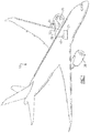
- FIG 1 illustrates an aircraft 10 including turbine engines 20. Included within the turbine engines 20 are multiple sensors 22, 24. Although only two sensors are illustrated for explanatory purposes, it is understood that many additional sensors are included in practical applications of turbine engines 20 and aircraft 10 designs. Each of the sensors 22, 24 output a sensor signal to a multiplexor 30 that is located in close proximity to the sensors 22, 24.
- the multiplexor 30 combines the sensor signals into a single signal using known multiplexing techniques, and transmits the signal to a signal processor 50, such as a controller via a multiplexed signal transmission line 32.
- the multiplexed signal transmission line 32 connects to the signal processor 50 via a signal conditioning block 40.
- the signal conditioning block 40 also includes an analog to digital converter, ensuring that the signal processor 50 receives digital signals that can be properly interpreted.
- the readings from the sensors 22, 24 need to be time correlated for proper operation of the controller.
- a time correlation logic circuit is utilized to time correlate the multiplexed data received by the signal processor 50.
- the time correlation logic circuit is located between the signal conditioning block 40 and the signal processor 50 and utilizes digital logic to time correlate the sensor signals.
- the time correlation circuit can be either a hardware based digital logic circuit, or a software based digital logic signal processing program.
- Figure 2 illustrates a sensor arrangement 100 for sensors 112, 114 where the sensors 112, 114 are sensing time correlated data.
- Each of the sensors 112, 114 transmits an independent sensor signal to a multiplexer 120.
- the multiplexer 120 multiplexes the sensor signals into a single signal using known multiplexor techniques, and transmits the multiplexed signal to a signal conditioner 130. Once conditioned the signal is converted into a digital signal in an analog to digital converter 140 and passed to a time correlation logic circuit 150.
- the time correlation logic circuit 150 reads the multiplexed sensor signals and determines a time correlated sensor signal including time correlated sensor information from both sensors 112, 114.
- the time correlation logic circuit 150 utilizes known logic circuits to time correlate the sensor data according to the method described below with regards to Figures 4-6 .
- the time correlation logic circuit 150 passes the time correlated sensor signal to a signal processor 160, such as a controller, which then interprets the sensed data and causes the engine to respond appropriately.
- a signal processor 160 such as a controller
- the signal conditioner 130 is located at the signal processor 160.
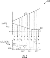
- Figure 3 is a graph 200 illustrating analog sensor signals 210, 220 on an analog graph portion 202 and multiplexed sensor signals 212, 222 on an analog to digital converter output graph portion 204.
- the multiplexor 120 alternates which signal is passed at each time period t 1 -t 8 .
- Each of the time periods t 1 -t 8 is the same length of time with the length being determined based on the needs and specification of the multiplexor 120.
- the analog sensor signal 210 from the first sensor 112 is passed as a multiplexed sensor value 212 at t 1 , t 3 , t 5 , and t 7 .
- the analog sensor value from the second sensor 114 is passed as a multiplexed sensor value 214 at t 2 , t 4 , t 6 , and t 8 .
- the multiplexor output signal shown on the analog to digital output graph 204 only one analog sensor signal 210, 220 is passed to the signal processor 160 any given time t 1 -t 8 , absent time correlation.
- the time correlation circuit 150 introduces a time delay and combines past and future values of the sensor signal 210, 220 that is not currently being passed by the multiplexed signal to determine a time correlated non-passed sensor value.
- the time correlated non-passed sensor value is combined with the passed sensor value to determine time correlated sensor signal.
- the time correlated sensor signal is then passed to the signal processor 160.
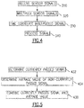
- Figure 4 illustrates the time correlation process performed by the time correlation logic circuit 150 illustrated in figure 2 .
- the signals from the sensors 112, 114 are received at the multiplexer 120 in a "receive sensor signals" step 310.
- the multiplexer 120 multiplexes the two sensor signals 210, 220 into a single multiplexed signal in a "multiplex sensor signals” step 320.
- the sensor signals 210, 220 are multiplexed together using standard multiplexer techniques. While the above described example utilizes only two sensors, it is understood that additional sensors could be multiplexed into the same signal and achieve the same benefits.
- the signal is passed through a signal conditioner 130 and an analog to digital converter 140 that converts the multiplexed signal into a digital signal that is readable by a signal processor 160, such as an engine controller.
- the digital multiplexed signal is time correlated in a time correlation logic circuit 150, prior to being passed to the signal processor 160, in a "time correlate multiplexed signal” step 330.
- An example process for performing the time correlate multiplexed signal step 330 is illustrated in Figure 5 and described below.
- the time correlated multiplexed signal is output from the time correlation circuit 150 and provided to the signal processor 160 in a "Process signal" step 340.
- Figure 5 illustrates a process by which the multiplexed sensor signals are time correlated to generate time correlated sensor information.
- the instantaneous value of the currently passed sensor for the time period is determined in a "determine currently passed signal" step 432. For example, if the current time frame is t 5 , the instantaneous value of the currently passed sensor signal 210, 222 is the actual value of the multiplexed signal, and corresponds to the actual value of the analog sensor signal 210 for the first analog sensor 112.
- the time correlation logic circuit 150 determines an average value of the non-passed sensor signal 220 in a "determine average value of non-passed sensor signal" step 434. To determine the average value of the non-passed sensor signal, the time correlation circuit 150 sums the value of the multiplexed signal from the previous time period (t 4 ) and the next time period (t 6 ) and divides the sum by 2. Utilization of the average value of the non-passed sensor signal 210, 220 necessarily introduces a time delay between the sensors and the receipt of the time correlated sensor signal at the signal processor.
- the time correlation logic circuit 150 extends two time periods from the current time period (t 5 ), and the average value of the non-currently passed signal is the sum of t 2 , t 4 , t 6 , and t 8 divided by four.
- the number of time periods utilized to determine the average of the non-currently passed value can be increased beyond four in a similar manner with the number of adjacent values to be utilized being determined based on the specifications of the particular implementation.
- the process combines the currently passed signal and the average value signal in a "combine currently passed signal and average value signal” step 436.
- the summation combines the two values, resulting in a single time correlated sensor output that can be received by the signal processor 160.
- C n is the time correlated signal value
- B n is the currently passed value of the multiplexed signal
- (A (n-1) + A (n+1) )/2 is the average value of the non-currently passed sensor signal.
- time correlation works well for linear sensed values, it is understood that sensor signals during acceleration or deceleration can include non-linear slopes requiring an alternate time correlation logic circuit 150.
- Figure 6 illustrates a process by which the time correlation logic circuit 150 compensates for acceleration or deceleration. Initially, the process determines the instantaneous slope of the currently passed sensor signal on the multiplexed signal in a "determine instantaneous slope of current signal” step 532. Once the instantaneous slope has been determined, the process determines an average slope value of non-currently passed signals in a "determine average slope value of non-currently passed signals” step 534. The average slope value is determined in a similar manner to the determination made in the "determine average value of non-currently passed signal” step 434 described above with regards to Figure 5 , with the rate of change of the non currently passed signal replacing the actual value of the non-currently passed signal.
- the process combines the instantaneous slope and average slope values from the previous steps 532, 534 to form a single combined time correlated output value in a "combine instantaneous slope and average slope" step 536.
- the process described in Figure 6 utilizes the first derivative of each of the sensor signals 210, 212 in place of the actual values.
- the second derivative of each value can be utilized in the above process.
Landscapes
- Engineering & Computer Science (AREA)
- Computer Networks & Wireless Communication (AREA)
- Physics & Mathematics (AREA)
- General Physics & Mathematics (AREA)
- Signal Processing (AREA)
- Arrangements For Transmission Of Measured Signals (AREA)
Claims (11)
- Verfahren zum Zeitkorrelieren eines multiplexierten Signals, das die folgenden Schritte umfasst:Empfangen eines multiplexierten Signals, das mindestens zwei Sensorsignale beinhaltet;Bestimmen eines Werts, der einen ersten der mindestens zwei Sensorsignale darstellt, wobei das erste der mindestens zwei Signale ein in Stromrichtung weitergeleiteter Wert des multiplexierten Signals zur Zeit t ist;Bestimmen eines Mittelwerts, der einen zweiten der mindestens zwei Sensorsignale darstellt, wobei das zweite der mindestens zwei Sensorsignale ein nicht in Stromrichtung weitergeleiteter Wert des multipexierten Signals zur Zeit t ist, wobei der Mittelwert ein Durchschnitt des Werts des zweiten der mindestens zwei Sensorsignale zu den Zeiten t-1 und t+1 ist;Kombinieren des Werts, der das erste der mindestens zwei Sensorsignale darstellt, und des Werts, der den zweiten der mindestens zwei Sensorsignale darstellt, zur Zeit t, wodurch ein zeitkorrelierter Sensorwert zur Zeit t bestimmt wird.
- Verfahren nach Anspruch 1, wobei der Schritt des Bestimmens eines Mittelwerts ferner das Teilen des Zwischensummenwerts durch die Anzahl der summierten Werte umfasst, wodurch der Mittelwert bestimmt wird, der das nicht in Stromrichtung weitergeleitete Signal für die Zeit t darstellt.
- Verfahren nach Anspruch 1, wobei der Schritt des Bestimmens eines Mittelwerts ferner das Summieren mindestens eines Anstiegs eines unmittelbar zuvor weitergeleiteten Werts des nicht in Stromrichtung weitergeleiteten multiplexierten Signals zur Zeit t-1 und eines Anstiegs eines unmittelbar danach weitergeleiteten Werts des nicht in Stromrichtung weitergeleiteten multiplexierten Signals zur Zeit t+1 umfasst, wodurch ein Zwischensummenwert bestimmt wird.
- Verfahren nach Anspruch 3, wobei der Schritt des Bestimmens eines Mittelwerts ferner das Teilen des Zwischensummenwerts durch die Anzahl der summierten Werte umfasst, wodurch der Mittelwert bestimmt wird, der das nicht in Stromrichtung weitergeleitete multiplexierte Signal für die Zeit t darstellt.
- Verfahren nach Anspruch 3, wobei ein Mittelwert, der ein nicht in Stromrichtung weitergeleitetes Signal zur Zeit t darstellt, eine Ableitung in Bezug auf eine Zeit des nicht in Stromrichtung weitergeleiteten multiplexierten Signals ist.
- Verfahren nach Anspruch 5, wobei der Wert, der einen in Stromrichtung weitergeleiteten Wert des multiplexierten Signals zur Zeit t darstellt, eine sofortige Ableitung des in Stromrichtung weitergeleiteten Werts des multiplexierten Signals ist.
- Sensorsystem, umfassend:einen ersten Sensor (112) und einen zweiten Sensor (114);einen Multiplexer (120), der mindestens zwei Multiplexereingänge aufweist, wobei ein erster Multiplexereingang mit einem Ausgang des ersten Sensors verbunden ist und der zweite Multiplexereingang mit einem Ausgang des zweiten Sensors verbunden ist;wobei ein Ausgang des Multiplexers über mindestens einen Signalaufbereitungs- und Anti-Aliasing-Filter (130) mit einer Zeitkorrelationslogikschaltung (150) verbunden ist;wobei ein Ausgang der Zeitkorrelationslogikschaltung mit einem Eingang eines Signalprozessors (160) verbunden ist; undwobei der Ausgang der Zeitkorrelationslogik eine zeitkorrelierte Sensorauslesung des ersten und des zweiten Sensors ist; wobei die Zeitkorrelationslogikschaltung einen Logikschaltkreis beinhaltet, der dazu konfiguriert ist, das Verfahren nach einem der vorhergehenden Ansprüche durchzuführen.
- Sensorsystem nach Anspruch 7, wobei der erste Sensor und der zweite Sensor analoge Sensoren sind.
- Sensorsystem nach Anspruch 7, wobei die Zeitkorrelationslogikschaltung hardwarebasiert ist.
- Sensorsystem nach Anspruch 8, wobei der Ausgang des Multiplexers über einen Signalaufbereitungs- und Anti-Aliasing-Filter, der mit einem Analog-Digital-Wandler (140) in Reihe geschaltet ist, mit der Zeitkorrelationslogikschaltung verbunden ist.
- Sensorsystem nach Anspruch 7, wobei die Zeitkorrelationslogikschaltung eine Beschleunigungskompensationslogikschaltung ist.
Applications Claiming Priority (1)
| Application Number | Priority Date | Filing Date | Title |
|---|---|---|---|
| US13/795,815 US9231719B2 (en) | 2013-03-12 | 2013-03-12 | Method and apparatus for multiplexed time aligned analog input sampling |
Publications (3)
| Publication Number | Publication Date |
|---|---|
| EP2779136A2 EP2779136A2 (de) | 2014-09-17 |
| EP2779136A3 EP2779136A3 (de) | 2017-05-17 |
| EP2779136B1 true EP2779136B1 (de) | 2019-07-24 |
Family
ID=50336072
Family Applications (1)
| Application Number | Title | Priority Date | Filing Date |
|---|---|---|---|
| EP14158545.5A Active EP2779136B1 (de) | 2013-03-12 | 2014-03-10 | Verfahren und Vorrichtung für multiplexierte, zeitlich abgestimmte Analogeingangsabtastung |
Country Status (2)
| Country | Link |
|---|---|
| US (1) | US9231719B2 (de) |
| EP (1) | EP2779136B1 (de) |
Families Citing this family (1)
| Publication number | Priority date | Publication date | Assignee | Title |
|---|---|---|---|---|
| US9710413B2 (en) * | 2013-06-28 | 2017-07-18 | Stmicroelectronics S.R.L. | Integrated data concentrator for multi-sensor MEMS systems |
Family Cites Families (14)
| Publication number | Priority date | Publication date | Assignee | Title |
|---|---|---|---|---|
| US4882614A (en) | 1986-07-14 | 1989-11-21 | Matsushita Electric Industrial Co., Ltd. | Multiplex signal processing apparatus |
| US5005142A (en) * | 1987-01-30 | 1991-04-02 | Westinghouse Electric Corp. | Smart sensor system for diagnostic monitoring |
| ATE213843T1 (de) * | 1996-05-14 | 2002-03-15 | Allied Signal Inc | Radargestützte boden- und hinderniswarnung |
| US6115654A (en) * | 1997-12-23 | 2000-09-05 | Simmonds Precision Products, Inc. | Universal sensor interface system and method |
| DE10022815A1 (de) * | 2000-05-10 | 2001-11-29 | Bosch Gmbh Robert | Vorrichtung zur Fehlererkennung bei einer digitalen Signalauswerteeinrichtung |
| US7149654B2 (en) | 2004-05-18 | 2006-12-12 | Honeywall International, Inc. | Sensor measurement method and system with universal data concentrators |
| US7432836B2 (en) | 2006-08-01 | 2008-10-07 | Hamilton Sundstrand Corporation | Multiplexed signal conditioner |
| DE102006038409B4 (de) | 2006-08-17 | 2009-07-09 | Infineon Technologies Ag | Verfahren und Vorrichtung zum Erfassen eines Analogsignals unter Verwendung einer Auswahlschaltung |
| EP2106058B1 (de) | 2008-03-28 | 2012-06-27 | TELEFONAKTIEBOLAGET LM ERICSSON (publ) | Verfahren und Anordnung zur Einstellung der Zeitanpassung eines abgetasteten Datenstroms |
| US8140242B2 (en) | 2008-05-22 | 2012-03-20 | United Technologies Corp. | Systems and methods involving multiplexed engine control signals |
| US7977936B2 (en) | 2008-10-16 | 2011-07-12 | Hamilton Sundstrand Corporation | Resolver interface and signal conditioner |
| US20130053983A1 (en) * | 2010-05-04 | 2013-02-28 | Achiam LIFSHITZ | Safe Artificial Joint |
| CN102959849B (zh) * | 2010-06-29 | 2015-11-25 | 伊顿工业公司 | 循环变流器的闭环控制 |
| KR101310596B1 (ko) * | 2011-12-15 | 2013-09-23 | 삼성전기주식회사 | 모션 감지장치 및 모션 감지방법 |
-
2013
- 2013-03-12 US US13/795,815 patent/US9231719B2/en active Active
-
2014
- 2014-03-10 EP EP14158545.5A patent/EP2779136B1/de active Active
Non-Patent Citations (1)
| Title |
|---|
| None * |
Also Published As
| Publication number | Publication date |
|---|---|
| US20140269775A1 (en) | 2014-09-18 |
| EP2779136A3 (de) | 2017-05-17 |
| EP2779136A2 (de) | 2014-09-17 |
| US9231719B2 (en) | 2016-01-05 |
Similar Documents
| Publication | Publication Date | Title |
|---|---|---|
| US9998825B2 (en) | Distributed automatic level control for a microphone array | |
| US10196152B2 (en) | Sensor data processing for condition monitoring systems | |
| TW200731160A (en) | GPU pipeline synchronization and control system and method | |
| EP2216626A1 (de) | Sensorgerät | |
| US8463963B2 (en) | Input/output device having hart communications functions | |
| EP2642363A3 (de) | Systeme und Verfahren zur Signalauswahl und Fehlererkennung | |
| WO2013143828A3 (de) | Interlockdetektor mit selbstdiagnosefunktion für einen interlockkreis und ein verfahren zur selbstdiagnose des interlockdetektors | |
| US9231719B2 (en) | Method and apparatus for multiplexed time aligned analog input sampling | |
| KR101473599B1 (ko) | 피드백 검사 분리 및 검사 바이패스 구조 | |
| EP1857937A1 (de) | Vorrichtung zur informationsverarbeitung und verfahren zur informationsverarbeitung | |
| US20190212715A1 (en) | Signal processing device and control method of signal processing device | |
| EP2009891A3 (de) | Übertragung eines Audiosignals in einem immersiven Audiokonferenzsystem | |
| ATE532271T1 (de) | Proaktives verstärkungsregelungssystem für kommunikationsempfänger | |
| MY197715A (en) | Voltage sensor diagnostic device and voltage sensor diagnostic method | |
| US20140050081A1 (en) | Reduced bandwidth transmission for multiple sensors utilized to monitor a system | |
| US7788440B2 (en) | Method and device for coupling at least two independent bus systems | |
| WO2014027366A3 (en) | System and method for analyzing arrangement of vehicle and building wire harnesses for emi | |
| US20180039379A1 (en) | Common mode noise processing method and apparatus | |
| JP6177590B2 (ja) | 模型用送受信システムの受信装置 | |
| JP4351162B2 (ja) | 位置測定装置を作動する方法とこのために適した位置測定装置 | |
| US10951450B2 (en) | Transmitter module, data transmission system and data transmission method | |
| KR20110080069A (ko) | 입출력 장치 및 그 제어 방법 | |
| US8150649B2 (en) | Method for operating an automation system | |
| US20090319205A1 (en) | Monitoring System, Especially Vibration Monitoring System, and Method for Operating Said System | |
| US7755507B2 (en) | Distributed control system and control device thereof |
Legal Events
| Date | Code | Title | Description |
|---|---|---|---|
| 17P | Request for examination filed |
Effective date: 20140310 |
|
| AK | Designated contracting states |
Kind code of ref document: A2 Designated state(s): AL AT BE BG CH CY CZ DE DK EE ES FI FR GB GR HR HU IE IS IT LI LT LU LV MC MK MT NL NO PL PT RO RS SE SI SK SM TR |
|
| AX | Request for extension of the european patent |
Extension state: BA ME |
|
| PUAI | Public reference made under article 153(3) epc to a published international application that has entered the european phase |
Free format text: ORIGINAL CODE: 0009012 |
|
| PUAL | Search report despatched |
Free format text: ORIGINAL CODE: 0009013 |
|
| AK | Designated contracting states |
Kind code of ref document: A3 Designated state(s): AL AT BE BG CH CY CZ DE DK EE ES FI FR GB GR HR HU IE IS IT LI LT LU LV MC MK MT NL NO PL PT RO RS SE SI SK SM TR |
|
| AX | Request for extension of the european patent |
Extension state: BA ME |
|
| RIC1 | Information provided on ipc code assigned before grant |
Ipc: G08C 15/00 20060101AFI20170413BHEP Ipc: H04Q 9/00 20060101ALI20170413BHEP |
|
| STAA | Information on the status of an ep patent application or granted ep patent |
Free format text: STATUS: REQUEST FOR EXAMINATION WAS MADE |
|
| R17P | Request for examination filed (corrected) |
Effective date: 20171117 |
|
| RBV | Designated contracting states (corrected) |
Designated state(s): AL AT BE BG CH CY CZ DE DK EE ES FI FR GB GR HR HU IE IS IT LI LT LU LV MC MK MT NL NO PL PT RO RS SE SI SK SM TR |
|
| GRAP | Despatch of communication of intention to grant a patent |
Free format text: ORIGINAL CODE: EPIDOSNIGR1 |
|
| STAA | Information on the status of an ep patent application or granted ep patent |
Free format text: STATUS: GRANT OF PATENT IS INTENDED |
|
| INTG | Intention to grant announced |
Effective date: 20190213 |
|
| RIN1 | Information on inventor provided before grant (corrected) |
Inventor name: SALOIO, JAMES Inventor name: HESS, GARY L. |
|
| RAP1 | Party data changed (applicant data changed or rights of an application transferred) |
Owner name: HAMILTON SUNDSTRAND CORPORATION |
|
| GRAS | Grant fee paid |
Free format text: ORIGINAL CODE: EPIDOSNIGR3 |
|
| GRAA | (expected) grant |
Free format text: ORIGINAL CODE: 0009210 |
|
| STAA | Information on the status of an ep patent application or granted ep patent |
Free format text: STATUS: THE PATENT HAS BEEN GRANTED |
|
| AK | Designated contracting states |
Kind code of ref document: B1 Designated state(s): AL AT BE BG CH CY CZ DE DK EE ES FI FR GB GR HR HU IE IS IT LI LT LU LV MC MK MT NL NO PL PT RO RS SE SI SK SM TR |
|
| REG | Reference to a national code |
Ref country code: GB Ref legal event code: FG4D |
|
| REG | Reference to a national code |
Ref country code: CH Ref legal event code: EP |
|
| REG | Reference to a national code |
Ref country code: DE Ref legal event code: R096 Ref document number: 602014050348 Country of ref document: DE |
|
| REG | Reference to a national code |
Ref country code: AT Ref legal event code: REF Ref document number: 1159131 Country of ref document: AT Kind code of ref document: T Effective date: 20190815 |
|
| REG | Reference to a national code |
Ref country code: IE Ref legal event code: FG4D |
|
| REG | Reference to a national code |
Ref country code: NL Ref legal event code: MP Effective date: 20190724 |
|
| REG | Reference to a national code |
Ref country code: LT Ref legal event code: MG4D |
|
| REG | Reference to a national code |
Ref country code: AT Ref legal event code: MK05 Ref document number: 1159131 Country of ref document: AT Kind code of ref document: T Effective date: 20190724 |
|
| PG25 | Lapsed in a contracting state [announced via postgrant information from national office to epo] |
Ref country code: FI Free format text: LAPSE BECAUSE OF FAILURE TO SUBMIT A TRANSLATION OF THE DESCRIPTION OR TO PAY THE FEE WITHIN THE PRESCRIBED TIME-LIMIT Effective date: 20190724 Ref country code: HR Free format text: LAPSE BECAUSE OF FAILURE TO SUBMIT A TRANSLATION OF THE DESCRIPTION OR TO PAY THE FEE WITHIN THE PRESCRIBED TIME-LIMIT Effective date: 20190724 Ref country code: NL Free format text: LAPSE BECAUSE OF FAILURE TO SUBMIT A TRANSLATION OF THE DESCRIPTION OR TO PAY THE FEE WITHIN THE PRESCRIBED TIME-LIMIT Effective date: 20190724 Ref country code: PT Free format text: LAPSE BECAUSE OF FAILURE TO SUBMIT A TRANSLATION OF THE DESCRIPTION OR TO PAY THE FEE WITHIN THE PRESCRIBED TIME-LIMIT Effective date: 20191125 Ref country code: BG Free format text: LAPSE BECAUSE OF FAILURE TO SUBMIT A TRANSLATION OF THE DESCRIPTION OR TO PAY THE FEE WITHIN THE PRESCRIBED TIME-LIMIT Effective date: 20191024 Ref country code: SE Free format text: LAPSE BECAUSE OF FAILURE TO SUBMIT A TRANSLATION OF THE DESCRIPTION OR TO PAY THE FEE WITHIN THE PRESCRIBED TIME-LIMIT Effective date: 20190724 Ref country code: LT Free format text: LAPSE BECAUSE OF FAILURE TO SUBMIT A TRANSLATION OF THE DESCRIPTION OR TO PAY THE FEE WITHIN THE PRESCRIBED TIME-LIMIT Effective date: 20190724 Ref country code: NO Free format text: LAPSE BECAUSE OF FAILURE TO SUBMIT A TRANSLATION OF THE DESCRIPTION OR TO PAY THE FEE WITHIN THE PRESCRIBED TIME-LIMIT Effective date: 20191024 Ref country code: AT Free format text: LAPSE BECAUSE OF FAILURE TO SUBMIT A TRANSLATION OF THE DESCRIPTION OR TO PAY THE FEE WITHIN THE PRESCRIBED TIME-LIMIT Effective date: 20190724 |
|
| PG25 | Lapsed in a contracting state [announced via postgrant information from national office to epo] |
Ref country code: ES Free format text: LAPSE BECAUSE OF FAILURE TO SUBMIT A TRANSLATION OF THE DESCRIPTION OR TO PAY THE FEE WITHIN THE PRESCRIBED TIME-LIMIT Effective date: 20190724 Ref country code: IS Free format text: LAPSE BECAUSE OF FAILURE TO SUBMIT A TRANSLATION OF THE DESCRIPTION OR TO PAY THE FEE WITHIN THE PRESCRIBED TIME-LIMIT Effective date: 20191124 Ref country code: LV Free format text: LAPSE BECAUSE OF FAILURE TO SUBMIT A TRANSLATION OF THE DESCRIPTION OR TO PAY THE FEE WITHIN THE PRESCRIBED TIME-LIMIT Effective date: 20190724 Ref country code: AL Free format text: LAPSE BECAUSE OF FAILURE TO SUBMIT A TRANSLATION OF THE DESCRIPTION OR TO PAY THE FEE WITHIN THE PRESCRIBED TIME-LIMIT Effective date: 20190724 Ref country code: GR Free format text: LAPSE BECAUSE OF FAILURE TO SUBMIT A TRANSLATION OF THE DESCRIPTION OR TO PAY THE FEE WITHIN THE PRESCRIBED TIME-LIMIT Effective date: 20191025 Ref country code: RS Free format text: LAPSE BECAUSE OF FAILURE TO SUBMIT A TRANSLATION OF THE DESCRIPTION OR TO PAY THE FEE WITHIN THE PRESCRIBED TIME-LIMIT Effective date: 20190724 |
|
| PG25 | Lapsed in a contracting state [announced via postgrant information from national office to epo] |
Ref country code: TR Free format text: LAPSE BECAUSE OF FAILURE TO SUBMIT A TRANSLATION OF THE DESCRIPTION OR TO PAY THE FEE WITHIN THE PRESCRIBED TIME-LIMIT Effective date: 20190724 |
|
| PG25 | Lapsed in a contracting state [announced via postgrant information from national office to epo] |
Ref country code: IT Free format text: LAPSE BECAUSE OF FAILURE TO SUBMIT A TRANSLATION OF THE DESCRIPTION OR TO PAY THE FEE WITHIN THE PRESCRIBED TIME-LIMIT Effective date: 20190724 Ref country code: EE Free format text: LAPSE BECAUSE OF FAILURE TO SUBMIT A TRANSLATION OF THE DESCRIPTION OR TO PAY THE FEE WITHIN THE PRESCRIBED TIME-LIMIT Effective date: 20190724 Ref country code: PL Free format text: LAPSE BECAUSE OF FAILURE TO SUBMIT A TRANSLATION OF THE DESCRIPTION OR TO PAY THE FEE WITHIN THE PRESCRIBED TIME-LIMIT Effective date: 20190724 Ref country code: RO Free format text: LAPSE BECAUSE OF FAILURE TO SUBMIT A TRANSLATION OF THE DESCRIPTION OR TO PAY THE FEE WITHIN THE PRESCRIBED TIME-LIMIT Effective date: 20190724 Ref country code: DK Free format text: LAPSE BECAUSE OF FAILURE TO SUBMIT A TRANSLATION OF THE DESCRIPTION OR TO PAY THE FEE WITHIN THE PRESCRIBED TIME-LIMIT Effective date: 20190724 |
|
| PG25 | Lapsed in a contracting state [announced via postgrant information from national office to epo] |
Ref country code: CZ Free format text: LAPSE BECAUSE OF FAILURE TO SUBMIT A TRANSLATION OF THE DESCRIPTION OR TO PAY THE FEE WITHIN THE PRESCRIBED TIME-LIMIT Effective date: 20190724 Ref country code: SK Free format text: LAPSE BECAUSE OF FAILURE TO SUBMIT A TRANSLATION OF THE DESCRIPTION OR TO PAY THE FEE WITHIN THE PRESCRIBED TIME-LIMIT Effective date: 20190724 Ref country code: SM Free format text: LAPSE BECAUSE OF FAILURE TO SUBMIT A TRANSLATION OF THE DESCRIPTION OR TO PAY THE FEE WITHIN THE PRESCRIBED TIME-LIMIT Effective date: 20190724 Ref country code: IS Free format text: LAPSE BECAUSE OF FAILURE TO SUBMIT A TRANSLATION OF THE DESCRIPTION OR TO PAY THE FEE WITHIN THE PRESCRIBED TIME-LIMIT Effective date: 20200224 |
|
| REG | Reference to a national code |
Ref country code: DE Ref legal event code: R097 Ref document number: 602014050348 Country of ref document: DE |
|
| PLBE | No opposition filed within time limit |
Free format text: ORIGINAL CODE: 0009261 |
|
| STAA | Information on the status of an ep patent application or granted ep patent |
Free format text: STATUS: NO OPPOSITION FILED WITHIN TIME LIMIT |
|
| PG2D | Information on lapse in contracting state deleted |
Ref country code: IS |
|
| 26N | No opposition filed |
Effective date: 20200603 |
|
| PG25 | Lapsed in a contracting state [announced via postgrant information from national office to epo] |
Ref country code: SI Free format text: LAPSE BECAUSE OF FAILURE TO SUBMIT A TRANSLATION OF THE DESCRIPTION OR TO PAY THE FEE WITHIN THE PRESCRIBED TIME-LIMIT Effective date: 20190724 |
|
| REG | Reference to a national code |
Ref country code: DE Ref legal event code: R119 Ref document number: 602014050348 Country of ref document: DE |
|
| PG25 | Lapsed in a contracting state [announced via postgrant information from national office to epo] |
Ref country code: MC Free format text: LAPSE BECAUSE OF FAILURE TO SUBMIT A TRANSLATION OF THE DESCRIPTION OR TO PAY THE FEE WITHIN THE PRESCRIBED TIME-LIMIT Effective date: 20190724 |
|
| REG | Reference to a national code |
Ref country code: CH Ref legal event code: PL |
|
| REG | Reference to a national code |
Ref country code: BE Ref legal event code: MM Effective date: 20200331 |
|
| PG25 | Lapsed in a contracting state [announced via postgrant information from national office to epo] |
Ref country code: LU Free format text: LAPSE BECAUSE OF NON-PAYMENT OF DUE FEES Effective date: 20200310 |
|
| PG25 | Lapsed in a contracting state [announced via postgrant information from national office to epo] |
Ref country code: CH Free format text: LAPSE BECAUSE OF NON-PAYMENT OF DUE FEES Effective date: 20200331 Ref country code: DE Free format text: LAPSE BECAUSE OF NON-PAYMENT OF DUE FEES Effective date: 20201001 Ref country code: IE Free format text: LAPSE BECAUSE OF NON-PAYMENT OF DUE FEES Effective date: 20200310 Ref country code: LI Free format text: LAPSE BECAUSE OF NON-PAYMENT OF DUE FEES Effective date: 20200331 |
|
| PG25 | Lapsed in a contracting state [announced via postgrant information from national office to epo] |
Ref country code: BE Free format text: LAPSE BECAUSE OF NON-PAYMENT OF DUE FEES Effective date: 20200331 |
|
| PG25 | Lapsed in a contracting state [announced via postgrant information from national office to epo] |
Ref country code: MT Free format text: LAPSE BECAUSE OF FAILURE TO SUBMIT A TRANSLATION OF THE DESCRIPTION OR TO PAY THE FEE WITHIN THE PRESCRIBED TIME-LIMIT Effective date: 20190724 Ref country code: CY Free format text: LAPSE BECAUSE OF FAILURE TO SUBMIT A TRANSLATION OF THE DESCRIPTION OR TO PAY THE FEE WITHIN THE PRESCRIBED TIME-LIMIT Effective date: 20190724 |
|
| PG25 | Lapsed in a contracting state [announced via postgrant information from national office to epo] |
Ref country code: MK Free format text: LAPSE BECAUSE OF FAILURE TO SUBMIT A TRANSLATION OF THE DESCRIPTION OR TO PAY THE FEE WITHIN THE PRESCRIBED TIME-LIMIT Effective date: 20190724 |
|
| P01 | Opt-out of the competence of the unified patent court (upc) registered |
Effective date: 20230522 |
|
| PGFP | Annual fee paid to national office [announced via postgrant information from national office to epo] |
Ref country code: GB Payment date: 20260219 Year of fee payment: 13 |
|
| PGFP | Annual fee paid to national office [announced via postgrant information from national office to epo] |
Ref country code: FR Payment date: 20260220 Year of fee payment: 13 |