EP2778765A2 - Ophthalmische Vorrichtungen mit photonischen Elementen zum Projizieren von Daten auf eine Retina - Google Patents
Ophthalmische Vorrichtungen mit photonischen Elementen zum Projizieren von Daten auf eine Retina Download PDFInfo
- Publication number
- EP2778765A2 EP2778765A2 EP14160132.8A EP14160132A EP2778765A2 EP 2778765 A2 EP2778765 A2 EP 2778765A2 EP 14160132 A EP14160132 A EP 14160132A EP 2778765 A2 EP2778765 A2 EP 2778765A2
- Authority
- EP
- European Patent Office
- Prior art keywords
- ophthalmic device
- light
- lens
- photonic
- light source
- Prior art date
- Legal status (The legal status is an assumption and is not a legal conclusion. Google has not performed a legal analysis and makes no representation as to the accuracy of the status listed.)
- Granted
Links
Images




Classifications
-
- G—PHYSICS
- G02—OPTICS
- G02C—SPECTACLES; SUNGLASSES OR GOGGLES INSOFAR AS THEY HAVE THE SAME FEATURES AS SPECTACLES; CONTACT LENSES
- G02C11/00—Non-optical adjuncts; Attachment thereof
- G02C11/10—Electronic devices other than hearing aids
-
- G—PHYSICS
- G02—OPTICS
- G02B—OPTICAL ELEMENTS, SYSTEMS OR APPARATUS
- G02B27/00—Optical systems or apparatus not provided for by any of the groups G02B1/00 - G02B26/00, G02B30/00
- G02B27/01—Head-up displays
- G02B27/017—Head mounted
-
- G—PHYSICS
- G02—OPTICS
- G02B—OPTICAL ELEMENTS, SYSTEMS OR APPARATUS
- G02B27/00—Optical systems or apparatus not provided for by any of the groups G02B1/00 - G02B26/00, G02B30/00
- G02B27/01—Head-up displays
- G02B27/017—Head mounted
- G02B27/0172—Head mounted characterised by optical features
-
- G—PHYSICS
- G02—OPTICS
- G02C—SPECTACLES; SUNGLASSES OR GOGGLES INSOFAR AS THEY HAVE THE SAME FEATURES AS SPECTACLES; CONTACT LENSES
- G02C7/00—Optical parts
- G02C7/02—Lenses; Lens systems ; Methods of designing lenses
- G02C7/04—Contact lenses for the eyes
Definitions
- This invention describes Ophthalmic Devices that have Photonic Emitters upon or within them.
- an ophthalmic device such as a contact lens, an intraocular lens, or a punctal plug, included a biocompatible device with a corrective, cosmetic, or therapeutic quality.
- a contact lens may provide one or more of vision correcting functionality, cosmetic enhancement, and therapeutic effects. Each function is provided by a physical characteristic of the lens.
- a design incorporating a refractive quality into a lens may provide a vision corrective function.
- a pigment incorporated into the lens may provide a cosmetic enhancement.
- An active agent incorporated into a lens may provide a therapeutic functionality. Such physical characteristics are accomplished without the lens entering into an energized state.
- a punctal plug has traditionally been a passive device.
- Novel ophthalmic devices based on energized and non-energized ophthalmic inserts have recently been described. These devices may use the energization function to power active optical components.
- nanoscale photonic elements may be useful in projecting photons from arrays of said elements.
- images may be obtained.
- ophthalmic devices it may be useful to define ophthalmic devices to result from the incorporation of nanoscale photonic elements or arrays of such elements into said ophthalmic devices.
- the present invention includes an encapsulated Media Insert with Photonic Emitters that may be included into an energized Ophthalmic Device, and in some embodiments, specifically, a contact lens.
- the Photonic Emitters may provide light patterns or dynamic images from light patterns that may be used to convey information or data through an ophthalmic device to a user's retina in the form of the light patterns.
- an energized Ophthalmic Device with a projection system comprising an array of Photonic Emitters where the image is filtered by a corresponding array of light modulating elements and projected through an electro-optic lens system is provided.
- the present invention therefore includes disclosure of Ophthalmic devices which contain Photonic Emitters.
- the Ophthalmic devices may additionally include light sources which provide light to the Photonic Emitters.
- the novel Ophthalmic devices may additionally include electronic components that control and pass energy in the form of electrical potential to the light source.
- the electronic components may receive their energy from energization elements. In some embodiments, these components may all be assembled in an Ophthalmic device that may have a size and shape that is consistent with the Ophthalmic device occupying a position that is between a user's eye surface and a that eye's respective eye lid.
- the Photonic Emitters of such a device may be formed in a semiconducting material which may include or be made of silicon.
- Designs of the Photonic Emitters may have numerous aspects useful to their function. For example, the incorporation of resistive heating elements in their structure may allow for Photonic Emitter elements that influence the phase characteristics of light that pass through them. Other design elements, such as the length and separation of portions of the Photonic Emitter relative to light pipes that provide photons to the system, may be important.
- the light sources that provide light to the Photonic Emitters and to the systems formed from combinations of these Photonic Emitters may be of different types. Some embodiments may be comprised of light emitting diodes for the light source. Other embodiments may comprise solid state laser elements as at least part of the light source. In some embodiments, the light source may be comprised of combinations of multiple light sources. The combination may be of Led and Laser sources or of individual sources of each type, where the individual sources may have different wavelength characteristics. For example, a solid-state light emitting element of either a diode type or a laser type may be one of at least the following color choices: Red, Orange, Yellow, Green, or Blue to mention some examples.
- the light source may be formed in or upon the same substrate as the Photonic Emitter in a processing flow that my in one flow process light sources, electronic components and optical components. In other embodiments, separate light source components may be attached to the systems comprising Photonic Emitters.
- the Ophthalmic device may include elements and systems of elements that act on the intensity of light emitted from a Photonic Emitter before it leaves the ophthalmic device.
- each Photonic Emitter may comprise a pixel element, and each pixel element may also have a Light Modulating Element.
- a combination of these light modulating elements may be considered a light modulating system.
- the system may be considered as a Pixel Based Light Modulating System.
- the Light Modulating Elements may function by interposing a material that filters light into the light path arising from the Photonic Emitters.
- this function may be performed using Electro-Wetting on Dielectric (EWOD) based phenomena, where a surface region within the device may be constructed to have a nascent surface free energy.
- EWOD device may then also have a combination of immiscible liquids or fluids that interact differently with the surface region of defined nascent surface free energy.
- a controlled application of an electro-potential across the surface region may be useful in altering its surface free energy or its effective surface free energy and thus interact with the combination of immiscible fluids differently.
- At least one of the fluids absorbs or scatters the light emanating from the Photonic Emitter and the other does not, by changing which fluids are or are not in the light path, a control or modulation of the light intensity may be obtained and this may be called light modulation.
- An Ophthalmic device may be formed by incorporating a projection system along with energization elements, control circuitry, communication circuitry and data processing circuitry into a single entity.
- the projection system may be made up of a subsystem comprising at least a Photonic Emitter element, a light source, a light modulating element and a lens element.
- the projection systems may also be made up of subsystems that comprise combinations of Photonic Emitter elements and an associated Pixel Based Light Modulating Elements.
- An ophthalmic device which incorporates a projection system, may display data or information in various forms.
- the display may project text-based information.
- the display may project images.
- the images may be of the form of digital images comprised of multiple pixels of image data projected.
- the images may be displayed as a monochrome display or alternatively have various degrees of color.
- the projection system may display data in the form of video of various formats.
- the exemplary display of an ophthalmic display comprising a system of Photonic Emitters may incorporate lenses as part of the ophthalmic device. These lenses may act on the image formed from the system of photonic emitters and focus that image in various ways onto the user's retina.
- the far field image created by the array of photonic emitters or the near field image created by the array of photonic emitters may be focused by the lens system.
- the lens system may comprise multiple lens subsystems.
- the lens subsystems may have elements that have a fixed focal characteristic or a fixed focal length.
- the lens subsystem may include at least a first variable focal length lens.
- variable focal length lens may include a meniscus-based lens that may also function utilizing the EWOD effect.
- Complex variable focal length lens may also be formed with multiple electrode regions that may be useful to move the focal point characteristic of the lens both from a focal length perspective but also from a translational perspective that may effectively vary where the image is projected.
- the image may be projected by the system through a user's eye and upon a user's retina.
- the size of the image formed by the extent of the imaged photonic elements may be less than a square centimeter in size. In other embodiments the size may be less than or approximately equal to a square millimeter in size.
- the present invention relates to an ophthalmic device having Photonic Emitters that may project light patterns in the environment of the eye.
- the Media Insert 100 may comprise an Optical Zone 120 that may or may not be functional to provide vision correction. Where the energized function of the ophthalmic device is unrelated to vision, the Optical Zone 120 of the Media Insert 100 may be void of material. In some embodiments, the Media Insert 100 may include a portion not in the Optical Zone 120 comprising a substrate 115 incorporated with energization elements 110 and electronic components 105. There may be numerous embodiments relating to including Photonic Emitters into ophthalmic devices.
- a power source 110 which may be, for example, a battery
- a load 105 which may be, for example, a semiconductor die
- Conductive traces 125 and 130 may electrically interconnect the electronic components 105 and the energization elements 110.
- the Media Insert 100 may be fully encapsulated to protect and contain the energization elements, traces, and electronic components.
- the encapsulating material may be semi-permeable, for example, to prevent specific substances, such as water, from entering the Media Insert 100 and to allow specific substances, such as ambient gasses or the byproducts of reactions within energization elements, to penetrate or escape from the Media Insert 100.
- the Media Insert 100 may be included in an ophthalmic device 150, which may comprise a polymeric biocompatible material.
- the ophthalmic device 150 may include a rigid center, soft skirt design wherein a central rigid optical element comprises the Media Insert 100.
- the Media Insert 100 may be in direct contact with the atmosphere and the corneal surface on respective anterior and posterior surfaces, or alternatively, the Media Insert 100 may be encapsulated in the ophthalmic device 150.
- the periphery 155 of the ophthalmic Lens 150 may be a soft skirt material, including, for example, a hydrogel material.
- the infrastructure of the media insert 100 and the ophthalmic device 150 may provide an environment for numerous embodiments involving light projection with Photonic Emitters, which may be combined with active or non-active lens devices and in some embodiments with light intensity modulating arrays. Some of these embodiments may involve purely passive function of the portion of the ophthalmic device not related to the photonic projection components. Other embodiments, may involve the ophthalmic device having active functions that may complement or supplement the function of the photonic projection components. For example, the non-projection portions of the device may provide vision correction or active "screening" of the device such that its transparency to incident light is reduced.
- item 200 a depiction of an exemplary multi-piece insert may be illustrated in cross section.
- the insert of this type is an annular insert with a ring of material around a central optical zone that is devoid of material.
- the ophthalmic device, 220 may have a cross sectional representation, 230, which represents a cross section through the location represented by line 210.
- the region of the insert outside the optic zone of the ophthalmic device may include energization elements and controlling electronics to support active elements of various kinds. These active elements may typically include sensors and communication elements of various types.
- inventive art herein may provide the control and energization function for a projection element based upon photonic projection elements.
- a projection element based upon photonic projection elements.
- outside the optic zone of the device there may be printed patterns placed on the insert as shown by item 221 and in cross section as items 231.
- Items 250 and 260 may represent stabilization zone features that can aid in orienting the formed ophthalmic lens upon a user's eye.
- orientation features upon the multi-piece annular insert may allow for its orientation relative to the molded stabilization features, which may be particularly important for placements of projection elements and lens systems that do not have dynamic focus and centering controls.
- the ophthalmic device, 320 may have a cross sectional representation, 330, which represents a cross section through the location represented by line 310.
- the optic zone of the ophthalmic device 320 may include a portion where an active focal adjusting lens system such as a liquid meniscus based lens system 335 may be found.
- an active focal adjusting lens system such as a liquid meniscus based lens system 335 may be found.
- portions of the insert that contain energization elements and control and activation components at 336.
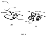
- Photonic Emitters are displayed. There may be numerous manners of defining emitter (which may also be considered radiator) elements for use with photonic applications.
- item 410 demonstrates a simple Photonic Emitter element consistent with some definitions described in the state of the art.
- the source of the photons for the system may be a light pipe 420 that runs parallel to coupling portions 430 of the radiator element. Photons travelling through the light pipe 420 may couple to the coupling portions 430 by a process which may be called evanescent coupling; an exponentially decaying phenomena in the near region to the periphery of the light pipe. The coupling will allow photons to move from the light pipe to the radiator element.
- the degree of the coupling and therefore the number of photons that enter the radiator element may be modulated by a number of phenomena such as the materials used, the ambient conditions but more importantly the structural design of the system.
- the length of the parallel portion of item 430 and the gap between this region and the light pipe, 435 may dominate the efficiency of coupling and can be used to adjust the nominal relative intensity of a Photonic Emitter in a collection of Photonic Emitters.
- the light will proceed through the element's light guiding components, 430 until it reaches the radiator portion shaped in a diffraction grating.
- a heating mechanism may be incorporated into the emitter cell. It may be comprised of a resistive heater built into the Photonic Emitter.
- the resistor may be formed in the same layer where it may be doped to alter resistivity characteristics.
- the Photonic Emitter of item 450 may have a certain intensity of light emitted from it based on the intensity in the source light pipe 420 and the efficiency of coupling of source light into the emitter device based on the proximity of a coupling region of the emitter device and the dimensions of that coupling region.
- the phase of that light may be controllably altered based on the application of an electrical current through the heater portion between item 460 and 480. Control of the relative phase of emitted light in such a manner may result in the effective transmission of information encoded in the phase characteristics being observable in the far field image of an array built with such Photonic Emitters where the phase of individual pixels may be controlled by the thermal state imposed on portions of the emitter device.
- the Photonic Emitter pixel 520 may be defined in a similar fashion to the elements at 410 or 450.
- the cells are depicted of the type in item 450.
- Light is supplied from a light source 540 that may in some embodiments be comprised of one or more laser elements emitting light into one or more supply light pipes for the Photonic Emitter array. Electrical current flowing through the heated portions of a pixel 520 may be introduced by conductive metal lines built into the Photonic Emitter in similar fashions to the metal lines in an integrated circuit.
- a set of word lines 530 may have corresponding bit lines 535 to allow the addressing of individual cells in an efficient fashion.
- the photonic array may be built into the silicon substrate useful to construct control electronics for the array itself.
- the exemplary pixel elements such as 520 may have a dimension about 9 microns by 9 microns or smaller.
- an array of 64 x 64 emitters may have a scale of roughly 0.5mm by 0.5 mm in size. The actual dimensions of the pixels may vary in a matrix and may be different for different targeted wavelengths of emission.
- a close up version of the light source and the supply light pipe or pipes, 540 may be shown.
- Light from a source, 561 may be guided into the light pipe.
- additional distribution elements in the form of additional light pipes may be found.
- Items 570, 571 and 572 may demonstrate light pipes coupled into the main supply light pipe and running roughly perpendicular to distribute light to rows of Photonic Emitters.
- the design aspects of the pipes and the individual pixel elements along the row may be optimized for each element so that a particular intensity pattern along the row and in the array may be obtained.
- the array may be designed such that the resulting emission intensity from each pixel is approximately the same for all elements.
- multiple light sources at different wavelengths may be used to impart light on a single source light pipe 540 or in some embodiments; the light pipe 540 may be comprised of multiple pipes.
- source 561 may comprise a red light source
- source 562 may comprise a green light source
- 563 may comprise a blue light source.
- sources of light consistent with the inventive art including solid state lasers, or solid state light emitting diodes, or filtered incandescent lamps as non limiting examples.
- the light source may be characterized by a desired coherence of the light output. Other embodiments may function with non-coherent light sources.
- the interaction of the rows of light pipes shown as item 570 may be controlled so that one light source is favored for a particular row. This may be controlled by the use of filtering materials in the region where the light pipe for a row 570 couples to the supply light pipe. Alternatively, if there are multiple supply light pipes, the pipes for the non-desired wavelengths for a particular light source may be blocked by absorbing material. There may be numerous materials that may be used to block the light coupling including metallic materials or the use of heavy doping levels in a semiconductor material.
- the multiple light sources may have a duty cycle. They may be turned on or off for their turn to use the source light pipes. In such an embodiment, there may not be a need for either multiple source lines or controls to funnel different light sources to different regions of the array.
- the design of the Photonic Emitter pixel may have to be performed in such a manner that is not optimized for a particular wavelength but optimized for all wavelengths employed.
- the pixel may be comprised by multiple emitters where one of the emitters may be optimized for a particular source.
- the individual pixels include phase shifting components within their design
- the resulting far field image may comprise an image constructed from the phase information within the individual pixels.
- An example of such an embodiment where a photonic array projecting far field phase controlled pixel images may be depicted in Fig. 6 , item 600.
- An ophthalmic insert 610 as has been described, which may contain energization elements, and control circuitry may control electrical signals through an electrical bus 630.
- this bus may be constructed of conductors with as little visible light absorbance characteristics as possible.
- ITO Indium Tin Oxide
- a projection system 620 may be located at the center of the optical zone and may comprise an array of Photonic Emitters as shown in item 650 along with control circuitry, light sources, and lensing elements to mention a few of the included components.
- An alternative embodiment may involve the use of the photonic array as an emitter of light where the phase characteristics are not the primary focus. Proceeding to Fig. 7 , item 700 an example of a pixel element 720 utilizing the exemplary Photonic Emitter without incorporated heater may be found. In some embodiments, the incorporation of the heater may still be desirable, but for example, it is not depicted. If the near field image of the resulting array is focused on a particular position, the light source may be part of a projection system where each pixel has an element that controls the transmitted intensity that proceeds from the emitter to the user's retina. In Fig. 7 , an example of a light intensity-controlling element aligned to each photonic emission element may be found.
- Electro-wetting on Dielectrics may be used to control intensity transmitted on a pixel-by-pixel basis.
- the technique acts on combinations of liquids by changing the surface free energy of surfaces near the liquids.
- Combinations of immiscible liquids where one liquid, for example is a polar liquid like an aqueous solution, and the other liquid is a non polar liquid like an oil may be effective for EWOD devices.
- One of these liquids may be formulated to be transparent to light in a particular desired wavelength regime whereas the other liquid may be opaque at those or all visible wavelengths.
- the liquid itself may have such properties, or the liquid may be combined with dying agents to result in the desired wavelength blocking effect. And, it may be possible to include different combinations of liquids with different inherent wavelength blocking capabilities in different pixel elements in the same device.
- an oil based non-aqueous liquid may comprise a dying agent to render an effective absorbance in a layer of an EWOD pixel cell that may be considered a Light Modulating Element.
- item 710 may comprise a pixel element where the oil-based liquid is located across the pixel and absorbs significant quantities of light.
- isolation structure 711 and 716 that define the edges of the pixel cell.
- the oil-based liquid may be that depicted as item 717 in the exemplary pixel based EWOD cell.
- a portion of the cell at item 713 may be coated with a material that has a surface free energy such that it may repel oil-based fluids.
- the aqueous fluid may be represented as item 718.
- the fluids would prefer to assume a location where the dyed oil based phase is localized across the interior region of the pixel away from surface 713, and therefore in the light path of light proceeding through the pixel.
- a combination of electrodes 715 and 714 along with a dielectric underlying or comprising the material of surface 713 allows for an application of an electro-potential across the two immiscible liquids. By applying an electro-potential across the electrodes, the free energy of surface 713 may be altered to attract the oil-based liquid of item 717 to it as may be observed at 720.
- This embodiment would therefore allow for the pixel-based control of light emanating from a Photonic Emitter to be passed on through.
- this may allow for a projection system to be formed from a combination of an array of Photonic Emitters each with a corresponding pixel element comprising an electro-wetting on dielectric cell to control transmittance.
- These embodiments may also comprise a light source, control electronics for both the light source and the pixel elements, and a lens system to focus the near field image at a desired location, which may comprise a user's retina.
- electro-wetting on dielectric cell may allow for the control of the transmittance of light near a Photonic Emitter.
- the example provided of the electro-wetting on dielectric based cell may have numerous alternatives including for example the reversal of the type of fluid that may comprise a dye or an inherent quality to block light.
- item 800 an alternative embodiment of an EWOD pixel based light intensity-modulating cell is depicted.
- the electrode in proximity to a surface along which a fluid will be attracted is not on the sidewall of a vertical structure but along one of the cell faces. Because the device may operate with light proceeding through this surface, the use of relatively transparent electrodes is important in such embodiments. As mentioned in previous discussions, the use of ITO as the material for the electrode may be an acceptable solution. As well, there may be modifications that allow the electrode to be located on the periphery of the EWOD cell face as well. Nevertheless, in Fig. 8 , item 810 may represent a cell where the light absorbing material is blocking the majority of the cell surface.
- Item 817 may represent a fluid with an absorbing characteristic this is either inherent or results from the use of dyes.
- Item 818 may represent the other fluid that may not significantly interact with light through the cell.
- Item 813 may represent a surface which has a defined surface free energy which may be either inherent or may result from processing designed to establish a surface characteristic.
- Item 812 may be an optional layer of dielectric material that may be present if item 813 is created either as an additional film upon a dielectric or as a surface modification of a dielectric.
- Item 814 may be an electrode useful in defining the region of the dielectric surface that is affected when an electro-potential is applied across the EWOD cell.
- Items 811 and 816 may be the structural containment that is used to define pixels.
- the state of the cell may be as depicted in item 820.
- the fluid moves to the edge of the pixel element as shown by 827 on the cell depiction. Therefore, it is moved out of the optical path and the pixel becomes more transparent to light through it.
- Item 910 may be an ophthalmic device capable of being worn on a user's eye surface. It may be formed of a hydrogel-based skirt 911 that completely surrounds in some embodiments, or partially surrounds or supports an insert device in other embodiments. In the depiction, the skirt 911 surrounds a fundamentally annular insert device 936. Sealed within the insert device 936 may be energization elements, electronic circuitry for control, activation, communication, processing and the like. The energization elements may be single use battery elements or rechargeable elements along with power control systems, which enable the recharging of the device. The components may be located in the insert device as discrete components or as stacked integrated devices with multiple active layers.
- the ophthalmic device may have structural and cosmetic aspects to it including, stabilization elements 950 and 960 which may be useful for defining orientation of the device upon the user's eye and for centering the device appropriately.
- the fundamentally annular device may have patterns printed upon one or more of its surfaces depicted as an iris pattern item 921 and in the cross section 930, along the line 915, as items 931.
- the insert device may have a photonic-based imaging system in a small region of the optical zone as shown as item 940.
- a 64x64 pixel imaging system may be formed with a size roughly 0.5 mm x 0.5 mm in size.
- item 940 may be a photonic projection component that may comprise photonic emitter elements; an EWOD based pixel transmittance control device, a light source or multiple light sources and electronics to control these components.
- the photonic-based imaging system may be attached to a lens system 950 and be connected to the annular insert component by a data and power interconnection bus 941.
- the lens system may be formed of static lens components that focus the near field image of the imaging system to a fixed location in space related to the body of the ophthalmic device.
- the lens system may also include active components.
- a meniscus based lens device with multiple electrode regions may be used to both translate the center of the projected image and adjust the focal power of the device to adjust the focus and effectively the size of the image projected.
- the lens device may have its own control electronics or alternatively it may be controlled and powered by either the photonic-based imaging component or the annular insert device or both.
- the display may be a 64 x 64 based projection system, but more or less pixels are easily within the scope of the inventive art, which may be limited by the size of the pixel elements and the ophthalmic device itself.
- the display may be useful for displaying dot matrix textual data, image data or video data.
- the lens system may be used to expand the effective pixel size of the display in some embodiments by rastering the projection system across the user's eye while displaying data.
- the display may be monochromatic in nature or alternatively have a color range based on multiple light sources.
- Data to be displayed may be communicated to the ophthalmic lens from an outside source, or data may originate from the ophthalmic device itself from sensors, or memory components for example. In some cases data may originate both from external sources with communication and from within the ophthalmic device itself.
Landscapes
- Physics & Mathematics (AREA)
- Health & Medical Sciences (AREA)
- General Physics & Mathematics (AREA)
- Optics & Photonics (AREA)
- Ophthalmology & Optometry (AREA)
- General Health & Medical Sciences (AREA)
- Acoustics & Sound (AREA)
- Otolaryngology (AREA)
- Prostheses (AREA)
- Eyeglasses (AREA)
- Mechanical Light Control Or Optical Switches (AREA)
- Optical Modulation, Optical Deflection, Nonlinear Optics, Optical Demodulation, Optical Logic Elements (AREA)
Applications Claiming Priority (1)
| Application Number | Priority Date | Filing Date | Title |
|---|---|---|---|
| US13/833,877 US9465236B2 (en) | 2013-03-15 | 2013-03-15 | Ophthalmic devices incorporating photonic elements |
Publications (3)
| Publication Number | Publication Date |
|---|---|
| EP2778765A2 true EP2778765A2 (de) | 2014-09-17 |
| EP2778765A3 EP2778765A3 (de) | 2014-10-29 |
| EP2778765B1 EP2778765B1 (de) | 2020-03-04 |
Family
ID=50272529
Family Applications (1)
| Application Number | Title | Priority Date | Filing Date |
|---|---|---|---|
| EP14160132.8A Active EP2778765B1 (de) | 2013-03-15 | 2014-03-14 | Ophthalmische Vorrichtungen mit photonischen Elementen zum Projizieren von Daten auf eine Retina |
Country Status (13)
| Country | Link |
|---|---|
| US (3) | US9465236B2 (de) |
| EP (1) | EP2778765B1 (de) |
| JP (2) | JP6403962B2 (de) |
| KR (1) | KR20140113445A (de) |
| CN (1) | CN104049385A (de) |
| AU (1) | AU2014201534A1 (de) |
| BR (1) | BR102014006378A2 (de) |
| CA (1) | CA2846698A1 (de) |
| HK (1) | HK1201939A1 (de) |
| IL (1) | IL231370A0 (de) |
| RU (1) | RU2650578C2 (de) |
| SG (1) | SG10201400608UA (de) |
| TW (1) | TWI629505B (de) |
Families Citing this family (9)
| Publication number | Priority date | Publication date | Assignee | Title |
|---|---|---|---|---|
| EP3331422A1 (de) * | 2015-08-07 | 2018-06-13 | Koninklijke Philips N.V. | Vorrichtung und system zum überwachen eines auges einer person |
| US10216008B2 (en) | 2015-12-31 | 2019-02-26 | International Business Machines Corporation | Saccade and vergence tracking for distance auto focus adjustment |
| US10687425B2 (en) | 2016-05-09 | 2020-06-16 | International Business Machines Corporation | Method of forming a plurality of electro-optical module assemblies |
| US10638613B2 (en) | 2016-05-09 | 2020-04-28 | International Business Machines Corporation | Method of forming a plurality of electro-optical module assemblies |
| US10670656B2 (en) * | 2016-05-09 | 2020-06-02 | International Business Machines Corporation | Integrated electro-optical module assembly |
| CN110114710B (zh) * | 2016-10-31 | 2020-11-27 | 德遁公司 | 毫微微投影仪光学系统 |
| US11543685B2 (en) * | 2017-03-07 | 2023-01-03 | David T. Markus | Method and apparatus for image spacing |
| US12032229B2 (en) * | 2017-10-13 | 2024-07-09 | Sony Corporation | Contact lens |
| KR102431963B1 (ko) * | 2022-04-19 | 2022-08-16 | 주식회사 셀리코 | 각막 신경 자극이 가능한 콘택트 렌즈의 제조 방법 |
Family Cites Families (35)
| Publication number | Priority date | Publication date | Assignee | Title |
|---|---|---|---|---|
| US5016958A (en) * | 1989-02-07 | 1991-05-21 | E. I. Du Pont De Nemours And Company | Optical switch having a phase change region therein |
| WO1993009450A1 (en) * | 1991-10-30 | 1993-05-13 | Rockwell Marshall A | Optical waveguide display system |
| JPH08274376A (ja) * | 1995-03-15 | 1996-10-18 | Texas Instr Inc <Ti> | シリコンに格子整合したiii−v化合物半導体エミッター |
| US5682210A (en) | 1995-12-08 | 1997-10-28 | Weirich; John | Eye contact lens video display system |
| US5715337A (en) * | 1996-09-19 | 1998-02-03 | The Mirco Optical Corporation | Compact display system |
| US6885818B2 (en) | 2001-07-30 | 2005-04-26 | Hewlett-Packard Development Company, L.P. | System and method for controlling electronic devices |
| US6768256B1 (en) * | 2001-08-27 | 2004-07-27 | Sandia Corporation | Photonic crystal light source |
| AU2003263881A1 (en) * | 2002-08-09 | 2004-02-25 | E-Vision, Llc | Electro-active contact lens system |
| JP2004138680A (ja) * | 2002-10-15 | 2004-05-13 | Ntt Advanced Technology Corp | 光デバイス |
| KR101293444B1 (ko) * | 2004-04-05 | 2013-08-05 | 리쿠아비스타 비.브이. | 전기습윤 효과를 기초로 한 디스플레이 디바이스 |
| JP2005311823A (ja) | 2004-04-23 | 2005-11-04 | Seiko Epson Corp | 表示装置 |
| US7375701B2 (en) * | 2004-07-01 | 2008-05-20 | Carestream Health, Inc. | Scanless virtual retinal display system |
| JP5110847B2 (ja) * | 2005-10-18 | 2012-12-26 | 株式会社半導体エネルギー研究所 | 表示装置 |
| EP1777690B1 (de) | 2005-10-18 | 2012-08-01 | Semiconductor Energy Laboratory Co., Ltd. | Anzeigevorrichtung |
| US20070171328A1 (en) * | 2005-11-21 | 2007-07-26 | Freeman Mark O | Substrate-guided display |
| US7542210B2 (en) | 2006-06-29 | 2009-06-02 | Chirieleison Sr Anthony | Eye tracking head mounted display |
| US8089995B2 (en) * | 2006-07-12 | 2012-01-03 | Oracle America, Inc. | Structures and methods for adjusting the wavelengths of lasers via temperature control |
| DE102006059400B4 (de) * | 2006-12-12 | 2019-12-24 | Seereal Technologies S.A. | Display-Einrichtung zur Erzeugung von Rekonstruktionen dreidimensionaler Darstellungen |
| MX2009008829A (es) | 2007-02-23 | 2011-10-28 | Pixeloptics Inc | Apertura dinamica oftalmica. |
| RU2328208C1 (ru) * | 2007-02-26 | 2008-07-10 | ГОУ ВПО "Саратовский государственный университет им. Н.Г. Чернышевского" | Лазерный конфокальный двухволновый ретинотомограф с девиацией частоты |
| WO2008109867A2 (en) | 2007-03-07 | 2008-09-12 | University Of Washington | Active contact lens |
| US8783931B2 (en) * | 2007-12-03 | 2014-07-22 | Rambus Delaware Llc | Light injection system and method for uniform luminosity of waveguide-based displays |
| WO2009094587A1 (en) | 2008-01-23 | 2009-07-30 | Deering Michael F | Eye mounted displays |
| JP5239393B2 (ja) * | 2008-02-26 | 2013-07-17 | ソニー株式会社 | 液体光学素子 |
| US20100149073A1 (en) * | 2008-11-02 | 2010-06-17 | David Chaum | Near to Eye Display System and Appliance |
| US20100014907A1 (en) * | 2008-07-15 | 2010-01-21 | David Richmond | Twist-open stain applicator dispenser method of use |
| JP2010107908A (ja) | 2008-10-31 | 2010-05-13 | Sony Corp | エレクトロウェッティング装置、可変焦点レンズ、光ピックアップ装置、光記録再生装置、液滴操作装置、光学素子、ズームレンズ、撮像装置、光変調装置、表示装置、ストロボ装置及びエレクトロウェッティング装置の駆動方法 |
| US7869116B2 (en) * | 2008-12-16 | 2011-01-11 | Industrial Technology Research Institute | Display device for improving image contrast |
| US8497515B1 (en) * | 2009-07-27 | 2013-07-30 | E. Mikhail Sagal | LED device with thermoelectric module |
| CN102804032B (zh) * | 2009-12-04 | 2015-09-09 | 派诺特公司 | 电控聚焦眼科装置 |
| AU2011210536A1 (en) | 2010-02-01 | 2012-09-13 | Conversion Energy Enterprises Inc. | Methods and devices for crosslinking of corneal collagen and for treatment of disorders of the eye |
| JP5434848B2 (ja) * | 2010-08-18 | 2014-03-05 | ソニー株式会社 | 表示装置 |
| US20120133957A1 (en) * | 2010-11-30 | 2012-05-31 | Widman Michael F | Laser confocal sensor metrology system |
| US9446262B2 (en) * | 2011-02-04 | 2016-09-20 | Johnson & Johnson Vision Care, Inc. | Apparatus and method for formation of an energized ophthalmic device for light therapy |
| EP2508935A1 (de) * | 2011-04-08 | 2012-10-10 | Nxp B.V. | Flexibler Augeneinsatz und Glukosemesssystem |
-
2013
- 2013-03-15 US US13/833,877 patent/US9465236B2/en active Active
-
2014
- 2014-03-06 IL IL231370A patent/IL231370A0/en unknown
- 2014-03-13 TW TW103108929A patent/TWI629505B/zh not_active IP Right Cessation
- 2014-03-13 SG SG10201400608UA patent/SG10201400608UA/en unknown
- 2014-03-13 KR KR1020140029409A patent/KR20140113445A/ko not_active Abandoned
- 2014-03-14 RU RU2014110017A patent/RU2650578C2/ru not_active IP Right Cessation
- 2014-03-14 EP EP14160132.8A patent/EP2778765B1/de active Active
- 2014-03-14 JP JP2014051301A patent/JP6403962B2/ja not_active Expired - Fee Related
- 2014-03-14 CA CA2846698A patent/CA2846698A1/en not_active Abandoned
- 2014-03-14 AU AU2014201534A patent/AU2014201534A1/en not_active Abandoned
- 2014-03-17 CN CN201410116118.0A patent/CN104049385A/zh active Pending
- 2014-03-17 BR BRBR102014006378-1A patent/BR102014006378A2/pt not_active IP Right Cessation
-
2015
- 2015-03-11 HK HK15102486.0A patent/HK1201939A1/en unknown
-
2016
- 2016-09-15 US US15/266,558 patent/US10317705B2/en active Active
-
2018
- 2018-03-29 JP JP2018064575A patent/JP6692848B2/ja not_active Expired - Fee Related
-
2019
- 2019-06-06 US US16/433,961 patent/US20190285914A1/en not_active Abandoned
Also Published As
| Publication number | Publication date |
|---|---|
| JP6692848B2 (ja) | 2020-05-13 |
| RU2650578C2 (ru) | 2018-04-16 |
| US20190285914A1 (en) | 2019-09-19 |
| CN104049385A (zh) | 2014-09-17 |
| EP2778765B1 (de) | 2020-03-04 |
| HK1201939A1 (en) | 2015-09-11 |
| KR20140113445A (ko) | 2014-09-24 |
| JP6403962B2 (ja) | 2018-10-10 |
| TWI629505B (zh) | 2018-07-11 |
| US20140268014A1 (en) | 2014-09-18 |
| JP2014182395A (ja) | 2014-09-29 |
| SG10201400608UA (en) | 2014-10-30 |
| RU2014110017A (ru) | 2015-09-20 |
| IL231370A0 (en) | 2014-08-31 |
| JP2018156083A (ja) | 2018-10-04 |
| US20170003522A1 (en) | 2017-01-05 |
| CA2846698A1 (en) | 2014-09-15 |
| EP2778765A3 (de) | 2014-10-29 |
| BR102014006378A2 (pt) | 2014-11-18 |
| TW201447374A (zh) | 2014-12-16 |
| US9465236B2 (en) | 2016-10-11 |
| AU2014201534A1 (en) | 2014-10-02 |
| US10317705B2 (en) | 2019-06-11 |
Similar Documents
| Publication | Publication Date | Title |
|---|---|---|
| AU2014201476B2 (en) | Methods and apparatus to form ophthalmic devices incorporating photonic elements | |
| US20200183188A1 (en) | Method and ophthalmic device for providing visual representations to a user | |
| US10317705B2 (en) | Ophthalmic devices incorporating photonic elements | |
| US9658469B2 (en) | Ophthalmic devices incorporating metasurface elements |
Legal Events
| Date | Code | Title | Description |
|---|---|---|---|
| 17P | Request for examination filed |
Effective date: 20140314 |
|
| AK | Designated contracting states |
Kind code of ref document: A2 Designated state(s): AL AT BE BG CH CY CZ DE DK EE ES FI FR GB GR HR HU IE IS IT LI LT LU LV MC MK MT NL NO PL PT RO RS SE SI SK SM TR |
|
| AX | Request for extension of the european patent |
Extension state: BA ME |
|
| PUAI | Public reference made under article 153(3) epc to a published international application that has entered the european phase |
Free format text: ORIGINAL CODE: 0009012 |
|
| PUAL | Search report despatched |
Free format text: ORIGINAL CODE: 0009013 |
|
| AK | Designated contracting states |
Kind code of ref document: A3 Designated state(s): AL AT BE BG CH CY CZ DE DK EE ES FI FR GB GR HR HU IE IS IT LI LT LU LV MC MK MT NL NO PL PT RO RS SE SI SK SM TR |
|
| AX | Request for extension of the european patent |
Extension state: BA ME |
|
| RIC1 | Information provided on ipc code assigned before grant |
Ipc: G02B 27/01 20060101ALI20140922BHEP Ipc: G02C 7/04 20060101AFI20140922BHEP |
|
| R17P | Request for examination filed (corrected) |
Effective date: 20150429 |
|
| RBV | Designated contracting states (corrected) |
Designated state(s): AL AT BE BG CH CY CZ DE DK EE ES FI FR GB GR HR HU IE IS IT LI LT LU LV MC MK MT NL NO PL PT RO RS SE SI SK SM TR |
|
| REG | Reference to a national code |
Ref country code: HK Ref legal event code: DE Ref document number: 1201939 Country of ref document: HK |
|
| STAA | Information on the status of an ep patent application or granted ep patent |
Free format text: STATUS: EXAMINATION IS IN PROGRESS |
|
| 17Q | First examination report despatched |
Effective date: 20180719 |
|
| GRAP | Despatch of communication of intention to grant a patent |
Free format text: ORIGINAL CODE: EPIDOSNIGR1 |
|
| STAA | Information on the status of an ep patent application or granted ep patent |
Free format text: STATUS: GRANT OF PATENT IS INTENDED |
|
| INTG | Intention to grant announced |
Effective date: 20190403 |
|
| GRAJ | Information related to disapproval of communication of intention to grant by the applicant or resumption of examination proceedings by the epo deleted |
Free format text: ORIGINAL CODE: EPIDOSDIGR1 |
|
| STAA | Information on the status of an ep patent application or granted ep patent |
Free format text: STATUS: EXAMINATION IS IN PROGRESS |
|
| INTC | Intention to grant announced (deleted) | ||
| GRAP | Despatch of communication of intention to grant a patent |
Free format text: ORIGINAL CODE: EPIDOSNIGR1 |
|
| STAA | Information on the status of an ep patent application or granted ep patent |
Free format text: STATUS: GRANT OF PATENT IS INTENDED |
|
| INTG | Intention to grant announced |
Effective date: 20190917 |
|
| GRAS | Grant fee paid |
Free format text: ORIGINAL CODE: EPIDOSNIGR3 |
|
| GRAA | (expected) grant |
Free format text: ORIGINAL CODE: 0009210 |
|
| STAA | Information on the status of an ep patent application or granted ep patent |
Free format text: STATUS: THE PATENT HAS BEEN GRANTED |
|
| AK | Designated contracting states |
Kind code of ref document: B1 Designated state(s): AL AT BE BG CH CY CZ DE DK EE ES FI FR GB GR HR HU IE IS IT LI LT LU LV MC MK MT NL NO PL PT RO RS SE SI SK SM TR |
|
| REG | Reference to a national code |
Ref country code: GB Ref legal event code: FG4D |
|
| REG | Reference to a national code |
Ref country code: CH Ref legal event code: EP |
|
| REG | Reference to a national code |
Ref country code: AT Ref legal event code: REF Ref document number: 1241070 Country of ref document: AT Kind code of ref document: T Effective date: 20200315 |
|
| REG | Reference to a national code |
Ref country code: DE Ref legal event code: R096 Ref document number: 602014061767 Country of ref document: DE |
|
| REG | Reference to a national code |
Ref country code: IE Ref legal event code: FG4D |
|
| PG25 | Lapsed in a contracting state [announced via postgrant information from national office to epo] |
Ref country code: RS Free format text: LAPSE BECAUSE OF FAILURE TO SUBMIT A TRANSLATION OF THE DESCRIPTION OR TO PAY THE FEE WITHIN THE PRESCRIBED TIME-LIMIT Effective date: 20200304 Ref country code: FI Free format text: LAPSE BECAUSE OF FAILURE TO SUBMIT A TRANSLATION OF THE DESCRIPTION OR TO PAY THE FEE WITHIN THE PRESCRIBED TIME-LIMIT Effective date: 20200304 Ref country code: NO Free format text: LAPSE BECAUSE OF FAILURE TO SUBMIT A TRANSLATION OF THE DESCRIPTION OR TO PAY THE FEE WITHIN THE PRESCRIBED TIME-LIMIT Effective date: 20200604 |
|
| REG | Reference to a national code |
Ref country code: NL Ref legal event code: MP Effective date: 20200304 |
|
| PG25 | Lapsed in a contracting state [announced via postgrant information from national office to epo] |
Ref country code: BG Free format text: LAPSE BECAUSE OF FAILURE TO SUBMIT A TRANSLATION OF THE DESCRIPTION OR TO PAY THE FEE WITHIN THE PRESCRIBED TIME-LIMIT Effective date: 20200604 Ref country code: HR Free format text: LAPSE BECAUSE OF FAILURE TO SUBMIT A TRANSLATION OF THE DESCRIPTION OR TO PAY THE FEE WITHIN THE PRESCRIBED TIME-LIMIT Effective date: 20200304 Ref country code: LV Free format text: LAPSE BECAUSE OF FAILURE TO SUBMIT A TRANSLATION OF THE DESCRIPTION OR TO PAY THE FEE WITHIN THE PRESCRIBED TIME-LIMIT Effective date: 20200304 Ref country code: SE Free format text: LAPSE BECAUSE OF FAILURE TO SUBMIT A TRANSLATION OF THE DESCRIPTION OR TO PAY THE FEE WITHIN THE PRESCRIBED TIME-LIMIT Effective date: 20200304 Ref country code: GR Free format text: LAPSE BECAUSE OF FAILURE TO SUBMIT A TRANSLATION OF THE DESCRIPTION OR TO PAY THE FEE WITHIN THE PRESCRIBED TIME-LIMIT Effective date: 20200605 |
|
| REG | Reference to a national code |
Ref country code: LT Ref legal event code: MG4D |
|
| PG25 | Lapsed in a contracting state [announced via postgrant information from national office to epo] |
Ref country code: NL Free format text: LAPSE BECAUSE OF FAILURE TO SUBMIT A TRANSLATION OF THE DESCRIPTION OR TO PAY THE FEE WITHIN THE PRESCRIBED TIME-LIMIT Effective date: 20200304 |
|
| PG25 | Lapsed in a contracting state [announced via postgrant information from national office to epo] |
Ref country code: LT Free format text: LAPSE BECAUSE OF FAILURE TO SUBMIT A TRANSLATION OF THE DESCRIPTION OR TO PAY THE FEE WITHIN THE PRESCRIBED TIME-LIMIT Effective date: 20200304 Ref country code: EE Free format text: LAPSE BECAUSE OF FAILURE TO SUBMIT A TRANSLATION OF THE DESCRIPTION OR TO PAY THE FEE WITHIN THE PRESCRIBED TIME-LIMIT Effective date: 20200304 Ref country code: SM Free format text: LAPSE BECAUSE OF FAILURE TO SUBMIT A TRANSLATION OF THE DESCRIPTION OR TO PAY THE FEE WITHIN THE PRESCRIBED TIME-LIMIT Effective date: 20200304 Ref country code: SK Free format text: LAPSE BECAUSE OF FAILURE TO SUBMIT A TRANSLATION OF THE DESCRIPTION OR TO PAY THE FEE WITHIN THE PRESCRIBED TIME-LIMIT Effective date: 20200304 Ref country code: IS Free format text: LAPSE BECAUSE OF FAILURE TO SUBMIT A TRANSLATION OF THE DESCRIPTION OR TO PAY THE FEE WITHIN THE PRESCRIBED TIME-LIMIT Effective date: 20200704 Ref country code: ES Free format text: LAPSE BECAUSE OF FAILURE TO SUBMIT A TRANSLATION OF THE DESCRIPTION OR TO PAY THE FEE WITHIN THE PRESCRIBED TIME-LIMIT Effective date: 20200304 Ref country code: PT Free format text: LAPSE BECAUSE OF FAILURE TO SUBMIT A TRANSLATION OF THE DESCRIPTION OR TO PAY THE FEE WITHIN THE PRESCRIBED TIME-LIMIT Effective date: 20200729 Ref country code: RO Free format text: LAPSE BECAUSE OF FAILURE TO SUBMIT A TRANSLATION OF THE DESCRIPTION OR TO PAY THE FEE WITHIN THE PRESCRIBED TIME-LIMIT Effective date: 20200304 Ref country code: CZ Free format text: LAPSE BECAUSE OF FAILURE TO SUBMIT A TRANSLATION OF THE DESCRIPTION OR TO PAY THE FEE WITHIN THE PRESCRIBED TIME-LIMIT Effective date: 20200304 |
|
| REG | Reference to a national code |
Ref country code: CH Ref legal event code: PL |
|
| REG | Reference to a national code |
Ref country code: AT Ref legal event code: MK05 Ref document number: 1241070 Country of ref document: AT Kind code of ref document: T Effective date: 20200304 |
|
| REG | Reference to a national code |
Ref country code: DE Ref legal event code: R097 Ref document number: 602014061767 Country of ref document: DE |
|
| REG | Reference to a national code |
Ref country code: BE Ref legal event code: MM Effective date: 20200331 |
|
| PG25 | Lapsed in a contracting state [announced via postgrant information from national office to epo] |
Ref country code: LU Free format text: LAPSE BECAUSE OF NON-PAYMENT OF DUE FEES Effective date: 20200314 Ref country code: MC Free format text: LAPSE BECAUSE OF FAILURE TO SUBMIT A TRANSLATION OF THE DESCRIPTION OR TO PAY THE FEE WITHIN THE PRESCRIBED TIME-LIMIT Effective date: 20200304 |
|
| PLBE | No opposition filed within time limit |
Free format text: ORIGINAL CODE: 0009261 |
|
| STAA | Information on the status of an ep patent application or granted ep patent |
Free format text: STATUS: NO OPPOSITION FILED WITHIN TIME LIMIT |
|
| PG25 | Lapsed in a contracting state [announced via postgrant information from national office to epo] |
Ref country code: IT Free format text: LAPSE BECAUSE OF FAILURE TO SUBMIT A TRANSLATION OF THE DESCRIPTION OR TO PAY THE FEE WITHIN THE PRESCRIBED TIME-LIMIT Effective date: 20200304 Ref country code: DK Free format text: LAPSE BECAUSE OF FAILURE TO SUBMIT A TRANSLATION OF THE DESCRIPTION OR TO PAY THE FEE WITHIN THE PRESCRIBED TIME-LIMIT Effective date: 20200304 Ref country code: CH Free format text: LAPSE BECAUSE OF NON-PAYMENT OF DUE FEES Effective date: 20200331 Ref country code: AT Free format text: LAPSE BECAUSE OF FAILURE TO SUBMIT A TRANSLATION OF THE DESCRIPTION OR TO PAY THE FEE WITHIN THE PRESCRIBED TIME-LIMIT Effective date: 20200304 Ref country code: LI Free format text: LAPSE BECAUSE OF NON-PAYMENT OF DUE FEES Effective date: 20200331 |
|
| 26N | No opposition filed |
Effective date: 20201207 |
|
| PG25 | Lapsed in a contracting state [announced via postgrant information from national office to epo] |
Ref country code: SI Free format text: LAPSE BECAUSE OF FAILURE TO SUBMIT A TRANSLATION OF THE DESCRIPTION OR TO PAY THE FEE WITHIN THE PRESCRIBED TIME-LIMIT Effective date: 20200304 Ref country code: PL Free format text: LAPSE BECAUSE OF FAILURE TO SUBMIT A TRANSLATION OF THE DESCRIPTION OR TO PAY THE FEE WITHIN THE PRESCRIBED TIME-LIMIT Effective date: 20200304 Ref country code: BE Free format text: LAPSE BECAUSE OF NON-PAYMENT OF DUE FEES Effective date: 20200331 |
|
| PG25 | Lapsed in a contracting state [announced via postgrant information from national office to epo] |
Ref country code: FR Free format text: LAPSE BECAUSE OF NON-PAYMENT OF DUE FEES Effective date: 20200504 |
|
| REG | Reference to a national code |
Ref country code: HK Ref legal event code: WD Ref document number: 1201939 Country of ref document: HK |
|
| PG25 | Lapsed in a contracting state [announced via postgrant information from national office to epo] |
Ref country code: TR Free format text: LAPSE BECAUSE OF FAILURE TO SUBMIT A TRANSLATION OF THE DESCRIPTION OR TO PAY THE FEE WITHIN THE PRESCRIBED TIME-LIMIT Effective date: 20200304 Ref country code: MT Free format text: LAPSE BECAUSE OF FAILURE TO SUBMIT A TRANSLATION OF THE DESCRIPTION OR TO PAY THE FEE WITHIN THE PRESCRIBED TIME-LIMIT Effective date: 20200304 Ref country code: CY Free format text: LAPSE BECAUSE OF FAILURE TO SUBMIT A TRANSLATION OF THE DESCRIPTION OR TO PAY THE FEE WITHIN THE PRESCRIBED TIME-LIMIT Effective date: 20200304 |
|
| PG25 | Lapsed in a contracting state [announced via postgrant information from national office to epo] |
Ref country code: MK Free format text: LAPSE BECAUSE OF FAILURE TO SUBMIT A TRANSLATION OF THE DESCRIPTION OR TO PAY THE FEE WITHIN THE PRESCRIBED TIME-LIMIT Effective date: 20200304 Ref country code: AL Free format text: LAPSE BECAUSE OF FAILURE TO SUBMIT A TRANSLATION OF THE DESCRIPTION OR TO PAY THE FEE WITHIN THE PRESCRIBED TIME-LIMIT Effective date: 20200304 |
|
| PGFP | Annual fee paid to national office [announced via postgrant information from national office to epo] |
Ref country code: IE Payment date: 20230209 Year of fee payment: 10 |
|
| PGFP | Annual fee paid to national office [announced via postgrant information from national office to epo] |
Ref country code: GB Payment date: 20230202 Year of fee payment: 10 |
|
| GBPC | Gb: european patent ceased through non-payment of renewal fee |
Effective date: 20240314 |
|
| PG25 | Lapsed in a contracting state [announced via postgrant information from national office to epo] |
Ref country code: GB Free format text: LAPSE BECAUSE OF NON-PAYMENT OF DUE FEES Effective date: 20240314 |
|
| PG25 | Lapsed in a contracting state [announced via postgrant information from national office to epo] |
Ref country code: IE Free format text: LAPSE BECAUSE OF NON-PAYMENT OF DUE FEES Effective date: 20240314 |
|
| PG25 | Lapsed in a contracting state [announced via postgrant information from national office to epo] |
Ref country code: IE Free format text: LAPSE BECAUSE OF NON-PAYMENT OF DUE FEES Effective date: 20240314 Ref country code: GB Free format text: LAPSE BECAUSE OF NON-PAYMENT OF DUE FEES Effective date: 20240314 |
|
| PGFP | Annual fee paid to national office [announced via postgrant information from national office to epo] |
Ref country code: DE Payment date: 20260204 Year of fee payment: 13 |